JP2012142594A - 半導体素子のための緩衝化基板 - Google Patents
半導体素子のための緩衝化基板 Download PDFInfo
- Publication number
- JP2012142594A JP2012142594A JP2012057317A JP2012057317A JP2012142594A JP 2012142594 A JP2012142594 A JP 2012142594A JP 2012057317 A JP2012057317 A JP 2012057317A JP 2012057317 A JP2012057317 A JP 2012057317A JP 2012142594 A JP2012142594 A JP 2012142594A
- Authority
- JP
- Japan
- Prior art keywords
- substrate
- buffer layer
- layer
- silicon layer
- silicon
- Prior art date
- Legal status (The legal status is an assumption and is not a legal conclusion. Google has not performed a legal analysis and makes no representation as to the accuracy of the status listed.)
- Pending
Links
Images


Classifications
-
- H—ELECTRICITY
- H10—SEMICONDUCTOR DEVICES; ELECTRIC SOLID-STATE DEVICES NOT OTHERWISE PROVIDED FOR
- H10P—GENERIC PROCESSES OR APPARATUS FOR THE MANUFACTURE OR TREATMENT OF DEVICES COVERED BY CLASS H10
- H10P14/00—Formation of materials, e.g. in the shape of layers or pillars
- H10P14/20—Formation of materials, e.g. in the shape of layers or pillars of semiconductor materials
- H10P14/29—Formation of materials, e.g. in the shape of layers or pillars of semiconductor materials characterised by the substrates
- H10P14/2901—Materials
-
- H—ELECTRICITY
- H10—SEMICONDUCTOR DEVICES; ELECTRIC SOLID-STATE DEVICES NOT OTHERWISE PROVIDED FOR
- H10P—GENERIC PROCESSES OR APPARATUS FOR THE MANUFACTURE OR TREATMENT OF DEVICES COVERED BY CLASS H10
- H10P14/00—Formation of materials, e.g. in the shape of layers or pillars
- H10P14/20—Formation of materials, e.g. in the shape of layers or pillars of semiconductor materials
- H10P14/24—Formation of materials, e.g. in the shape of layers or pillars of semiconductor materials using chemical vapour deposition [CVD]
-
- H—ELECTRICITY
- H10—SEMICONDUCTOR DEVICES; ELECTRIC SOLID-STATE DEVICES NOT OTHERWISE PROVIDED FOR
- H10P—GENERIC PROCESSES OR APPARATUS FOR THE MANUFACTURE OR TREATMENT OF DEVICES COVERED BY CLASS H10
- H10P14/00—Formation of materials, e.g. in the shape of layers or pillars
- H10P14/20—Formation of materials, e.g. in the shape of layers or pillars of semiconductor materials
- H10P14/32—Formation of materials, e.g. in the shape of layers or pillars of semiconductor materials characterised by intermediate layers between substrates and deposited layers
- H10P14/3202—Materials thereof
- H10P14/3238—Materials thereof being insulating materials
-
- H—ELECTRICITY
- H10—SEMICONDUCTOR DEVICES; ELECTRIC SOLID-STATE DEVICES NOT OTHERWISE PROVIDED FOR
- H10P—GENERIC PROCESSES OR APPARATUS FOR THE MANUFACTURE OR TREATMENT OF DEVICES COVERED BY CLASS H10
- H10P14/00—Formation of materials, e.g. in the shape of layers or pillars
- H10P14/20—Formation of materials, e.g. in the shape of layers or pillars of semiconductor materials
- H10P14/34—Deposited materials, e.g. layers
- H10P14/3402—Deposited materials, e.g. layers characterised by the chemical composition
- H10P14/3404—Deposited materials, e.g. layers characterised by the chemical composition being Group IVA materials
- H10P14/3411—Silicon, silicon germanium or germanium
-
- H—ELECTRICITY
- H10—SEMICONDUCTOR DEVICES; ELECTRIC SOLID-STATE DEVICES NOT OTHERWISE PROVIDED FOR
- H10P—GENERIC PROCESSES OR APPARATUS FOR THE MANUFACTURE OR TREATMENT OF DEVICES COVERED BY CLASS H10
- H10P14/00—Formation of materials, e.g. in the shape of layers or pillars
- H10P14/20—Formation of materials, e.g. in the shape of layers or pillars of semiconductor materials
- H10P14/38—Formation of materials, e.g. in the shape of layers or pillars of semiconductor materials characterised by treatments done after the formation of the materials
- H10P14/3802—Crystallisation or recrystallisation of non-monocrystalline semiconductor materials, e.g. regrowth
- H10P14/3808—Crystallisation or recrystallisation of non-monocrystalline semiconductor materials, e.g. regrowth using laser beams
-
- Y—GENERAL TAGGING OF NEW TECHNOLOGICAL DEVELOPMENTS; GENERAL TAGGING OF CROSS-SECTIONAL TECHNOLOGIES SPANNING OVER SEVERAL SECTIONS OF THE IPC; TECHNICAL SUBJECTS COVERED BY FORMER USPC CROSS-REFERENCE ART COLLECTIONS [XRACs] AND DIGESTS
- Y10—TECHNICAL SUBJECTS COVERED BY FORMER USPC
- Y10S—TECHNICAL SUBJECTS COVERED BY FORMER USPC CROSS-REFERENCE ART COLLECTIONS [XRACs] AND DIGESTS
- Y10S438/00—Semiconductor device manufacturing: process
- Y10S438/967—Semiconductor on specified insulator
-
- Y—GENERAL TAGGING OF NEW TECHNOLOGICAL DEVELOPMENTS; GENERAL TAGGING OF CROSS-SECTIONAL TECHNOLOGIES SPANNING OVER SEVERAL SECTIONS OF THE IPC; TECHNICAL SUBJECTS COVERED BY FORMER USPC CROSS-REFERENCE ART COLLECTIONS [XRACs] AND DIGESTS
- Y10—TECHNICAL SUBJECTS COVERED BY FORMER USPC
- Y10T—TECHNICAL SUBJECTS COVERED BY FORMER US CLASSIFICATION
- Y10T428/00—Stock material or miscellaneous articles
- Y10T428/24—Structurally defined web or sheet [e.g., overall dimension, etc.]
- Y10T428/24479—Structurally defined web or sheet [e.g., overall dimension, etc.] including variation in thickness
-
- Y—GENERAL TAGGING OF NEW TECHNOLOGICAL DEVELOPMENTS; GENERAL TAGGING OF CROSS-SECTIONAL TECHNOLOGIES SPANNING OVER SEVERAL SECTIONS OF THE IPC; TECHNICAL SUBJECTS COVERED BY FORMER USPC CROSS-REFERENCE ART COLLECTIONS [XRACs] AND DIGESTS
- Y10—TECHNICAL SUBJECTS COVERED BY FORMER USPC
- Y10T—TECHNICAL SUBJECTS COVERED BY FORMER US CLASSIFICATION
- Y10T428/00—Stock material or miscellaneous articles
- Y10T428/24—Structurally defined web or sheet [e.g., overall dimension, etc.]
- Y10T428/24802—Discontinuous or differential coating, impregnation or bond [e.g., artwork, printing, retouched photograph, etc.]
- Y10T428/24926—Discontinuous or differential coating, impregnation or bond [e.g., artwork, printing, retouched photograph, etc.] including ceramic, glass, porcelain or quartz layer
-
- Y—GENERAL TAGGING OF NEW TECHNOLOGICAL DEVELOPMENTS; GENERAL TAGGING OF CROSS-SECTIONAL TECHNOLOGIES SPANNING OVER SEVERAL SECTIONS OF THE IPC; TECHNICAL SUBJECTS COVERED BY FORMER USPC CROSS-REFERENCE ART COLLECTIONS [XRACs] AND DIGESTS
- Y10—TECHNICAL SUBJECTS COVERED BY FORMER USPC
- Y10T—TECHNICAL SUBJECTS COVERED BY FORMER US CLASSIFICATION
- Y10T428/00—Stock material or miscellaneous articles
- Y10T428/26—Web or sheet containing structurally defined element or component, the element or component having a specified physical dimension
- Y10T428/263—Coating layer not in excess of 5 mils thick or equivalent
- Y10T428/264—Up to 3 mils
- Y10T428/265—1 mil or less
Landscapes
- Recrystallisation Techniques (AREA)
- Thin Film Transistor (AREA)
- Crystals, And After-Treatments Of Crystals (AREA)
Abstract
行なうための技術を提供する。
【解決手段】基板100上に形成したシリコン層104をレーザビーム106の照射によ
って結晶化して多結晶シリコン層108を得る半導体装置などに用いられ、基板100と
シリコン層104との間にバッファ層102が形成されている。バッファ層102を有す
るこのようなバッファ化基板において、該バッファ層102は、基板100の限界温度よ
りも高い融点を有し、さらに、シリコン層104の結晶化に際し、バッファ層102上に
均一なシリコン結晶粒子を形成するためシリコン層104の核生成密度を規定し、かつシ
リコン層104の結晶化過程における等方粒成長の基礎として機能する。
【選択図】図2
Description
つ多結晶層を形成するための構成と方法に関する。
も小型化していく。これに応じて多結晶シリコンの粒径および粒径バラツキが多結晶シリ
コン素子の特性上より重要な因子になる。特にTFTの外形寸法が小さくなるにしたがい
より微小な結晶粒が必要になり、これにより統計的に有意な数の粒子がTFTのチャンネ
ル領域に得られ、多結晶シリコン層に形成されたTFTの均一な素子特性が確保される。
例えばTFTの外形寸法に比べて相対的に粒径が大きくかつ粒径バラツキも大であると、
チャンネル領域に含まれる粒界の数に基づいたTFT特性にバラツキが生じる。
る。しかしながら、このようなレーザ結晶化技術により作製された多結晶層は、巨大な粒
径並びに粒径バラツキに加えて望ましくない粗な多結晶シリコン膜表面を有するという問
題があった。レーザ結晶化法においては、レーザビームによってアモルファスシリコン層
が融解され、次いで融解したシリコンが冷却することにより多結晶シリコン層が形成され
る。一般にレーザ結晶化法では10%の出力バラツキをもつパルスレーザが使用される。
しかし、このバラツキは多結晶シリコン層中に1000%の粒径バラツキの発生をもたら
す。このため従来のパルスレーザ結晶化法で作製されたTFT構成中の粒子数は著しく変
動する。
e)を用いて行われていた。この方式においては多結晶シリコンの粒径はレーザ出力(laser
fluence)依存性がきわめて高い。この現象についていくつかの理論付けがなされている
。すなわち臨界レーザ出力論「The critical laser fluence」(ジョンソン他著、Materi
als Research Society Symposium Proceedings:マテリアルズリサーチソサエティシンポ
ジウムプロシーディングス297巻、533頁、1993年)、側方成長論「lateral gr
owth」(クリヤマ他著、Japanese Journal of Applied Physics Letters:ジャパニーズ
ジャーナルオブアプライドフィジックスレターズ33巻、5657頁、1994年)およ
び超側方成長論「super lateral growth」(イム「Im」他著、Applied Physics Letters
:アプライドフィジックスレターズ64巻、2303頁、1994年)である。これらの
理論によると、狭いレーザ出力域でシリコン結晶粒は側方に大きく(シリコン膜の厚さの
約10倍の寸法に)成長する。この大きな側方粒成長はしばしば表面の凹凸が激しい場合
に発生する。
ため小型TFT用の粒子を統計的に有意な数で得ることができなくなる。さらに、100
nm厚さの結晶化多結晶シリコン層における巨大結晶粒の二乗平均(rms)表面粗度は
約60nmである。rms表面粗度がこのように大きいと絶縁破壊が発生するため高い素
子バイアス電圧を維持できない。
の粒径の均一性の改善が行われてきた。しかし基板加熱は製造工程における追加作業を必
要とし、このために素子製造に要する工程時間が増加して結果的に製造価格の高額化を招
く。
増加することなく多結晶シリコン粒径の微小化と均一化を行なうための技術を提案するこ
とを目的とする。
buffer layer、以下バッファ層という)を設けた緩衝化基板(buffered substrate、以下
バッファ化基板という)を用いることを特徴とする。このバッファ化基板は、基板、基板
上に形成されたバッファ層およびバッファ層上に形成されたシリコン層を含む。このシリ
コン層はバッファ層上に形成された後、レーザビームを用いて結晶化される。ここで、バ
ッファ層は基板の限界温度(threshlod temperature)、即ち基板の耐熱限界温度以上の
融点を有し、さらに、前記シリコン層の結晶化に際し、該バッファ層上に均一なシリコン
結晶粒子を形成するために、前記シリコン層の核生成密度を規定し、かつ前記シリコン層
の結晶化過程における等方粒成長の基礎として機能する。
ある。また、バッファ層の構成材料としては、例えば、MgO、MgAl2O4、Al2O3
およびZrO2が適用可能である。更に、バッファ層上に最初に形成されるシリコン層と
しては、アモルファスシリコン層が、またこのアモルファスシリコン層の厚みは、約10
0nmが適用可能である。
。また、結晶化シリコン層は、基板上のバッファ層の上にシリコン層を形成した後、レー
ザビームを用いて結晶化することによって得られる。
傍での不均質な核生成(heterogeneous nucleation)が欠乏することに起因する。この不
均質核生成の欠乏は、多結晶シリコン結晶粒子の巨大な側方成長をもたらす。同側方成長
は狭いレーザ出力範囲で発生し、寸法はシリコン層の厚さの約10倍である。この巨大な
側方粒成長はしばしば表面の凹凸が激しい場合に発生する。
響を受ける。このレーザ出力に対する敏感さは粒径バラツキ発生の主因であり、シリコン
が未溶融シリコンに接触した状態で結晶化する場合と、下地基板に接触した状態で結晶化
する場合における核生成密度の相違に起因するものである。レーザ出力の強度がシリコン
層を部分的に貫通溶融(メルトスルー:melt-through)し得る程度である場合、基板に接
した状態の溶融シリコンは、接していない状態のものとは異なる核生成密度をもつ。レー
ザ出力をシリコン層全体を貫通溶融するためのしきい値以上に設定して均一な核生成密度
を得ようとすると、多くの場合基板が損傷を受けると共に多結晶シリコン層のアブレーシ
ョン(ablation:融除)などの悪影響が生じる。
いて、基板とシリコン層の間にバッファ層を設けることで、結晶化によって得られる多結
晶シリコン結晶の粒径と粒径バラツキを減少させる。バッファ層は、基板の限界温度(基
板の耐熱限界温度)以上の耐熱性をもつ材料から形成される。基板がその限界温度以上に
加熱されると、基板のアブレーションや基板上に形成された膜のアブレーションが起こる
といった悪影響が生じる。そこでバッファ層によって上記悪影響から基板を保護する。例
えばSiO2は、約1610℃〜1723℃の間に融点をもつ。したがって1723℃以
上の融点をもつ材料がSiO2基板のバッファ層として使用されうる。
生成の基礎にもなる。基板と溶融シリコン界面に大量の核が存在すると、結晶化は多結晶
シリコン薄膜の厚さにほぼ等しい大きさの結晶粒を形成するように進行する。この現象は
等方粒成長(isotropic grain growth)と呼ばれる。バッファ層はシリコンの等方粒成長
を促進するものである。等方粒成長の増加により巨大な側方成長が抑制され、横方向、つ
まり面方向の粒子サイズが多結晶シリコン膜の厚さと同程度まで低減される。
作用によりシリコン粒子の微小化と粒径の均一化がなされる。多数の微小なシリコン粒子
が、形成される素子寸法に対して統計的に有意な数の粒子となる。素子当りの粒子数の増
加は素子特性の均一性を高め、結果的に素子の適用製品の信頼性を高める。
能な材料全てを網羅するものではない。
ァ層により、レーザ照射で生じる基板の損傷に対する耐性が付与される。
。同TFTは活性層下の基板上にゲート電極が形成されるため、基板の損傷によって漏洩
電流が発生する。ゲート電極が基板とバッファ層の間にあれば、このバッファ層は基板を
熱的に保護しつつボトムゲートTFTのゲート絶縁層として機能する。このようにバッフ
ァ層により素子特性が改善される。
バッファ層は、要求される熱的境界条件に応じて単層あるいは多層のいずれでも形成する
ことができる。また別の効果として、融解処理時間の延長、又は類似の他の処置による熱
的損傷から基板を保護する事がある。
リコン層は低アスペクト比(ほとんど1に近い)の粒子領域と高アスペクト比の粒子領域
とをもつ。粒子のアスペクト比とは粒子の幅と高さとの比率の事である。図1は該多結晶
シリコン層のTEM写真を示す図の一例である。等方粒成長と側方粒成長とによって得ら
れた多結晶シリコン膜の粒径バラツキは、側方結晶粒子と等方結晶粒子との粒径の違いに
ほぼ等しい。例えば、厚さ100nmのシリコン膜での側方成長においては、約100n
m径の等方結晶粒子の基質中にしばしば1μm径の粒子が生成する。すなわち約10倍の
粒径バラツキが発生する。
リコン層の厚み以下の多結晶シリコン層を提供する。
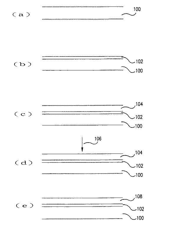
。図2(a)は石英あるいはガラス等の材料で形成された基板100を示すものである。
この基板100の材料としては、例えばSiO2、コーニング7059または1731な
どがある(コーニング7059または1731は一般的な基板材料であり、コーニンググ
ラスワークス社(ニューヨーク コーニング、14830)から容易に入手できる)。基
板100は他の構成、例えばボトムゲート素子のゲート誘電体やゲート電極などを含んで
いてもよい。
ッファ層102の形成は物理気相成長、化学気相成長(CVD)あるいはゾルゲル法など
の技術により行われる。物理気相成長法として、電子ビーム蒸着、スパッタ、加熱蒸着、
パルスレーザ蒸着等がある。薄膜バッファ層102は単層でよく、場合によっては基板1
00表面を必ずしも完全に覆う必要はない。バッファ層102が基板100表面を部分的
に覆ってアイランド状になる場合は、アイランドの密度が当該多結晶シリコン層に必要な
粒子の密度にほぼ一致することが必要である。
バッファ層102上に形成される。他の厚さのバッファ層も適用可能である。課題に即し
た素子としては約100nm以下の厚さのアモルファスシリコン層がパルスレーザ結晶化
処理用として適する。またシリコン層は非晶質でなくてもよい。この理由はレーザビーム
がシリコン層を融解し、融解前の結晶構造をすべて解消するためである。
とにより結晶化し、多結晶層108が形成される。各々の工程を図2(d)、図2(e)
に示す。レーザビーム106はYAGレーザあるいはエキシマレーザ等のレーザ装置から
発振される。多くの場合エキシマレーザが好適である。この理由は同レーザは照射範囲が
広いため処理速度が早いことによる。
験結果から、約540±20mJ/cm2あるいは全レーザ出力域の約10%の狭いレー
ザ出力域で側方粒成長が生じることが判明している。この狭いレーザ出力域はレーザ結晶
化の施工に必要なレーザ出力分布のほぼ中央に位置するものである。したがって巨大粒径
を防止するためには、狭いレーザ出力域内でのレーザ出力の変動を抑制する必要がある。
しかし素子作製に用いる工業用レーザの出力制御は困難であるため、工業用レーザでのレ
ーザ出力においては側方成長が生じる出力域を避ける必要がある。このため結晶化処理に
適用可能な工業用レーザの出力域は著しく制限される。
バッファ層によって生起されるシリコン粒子の核生成の作用により側方粒成長が抑制され
る。基本的には、バッファ層が存在する時には100nm厚さのシリコン膜を貫通溶融(
約300mJ/cm2)から融除(約600mJ/cm2)するまでの全レーザ出力範囲が
適用可能である。すなわちバッファ層を用いる事で著しく広範囲のレーザ出力が適用可能
になる。
ツキは概ね2以下である。これに対し従来技術による粒径バラツキは約10である。つま
りバッファ層102により粒径バラツキが5分の1以下に減少する。
に形成される素子の特性の均一性が著しく向上する。TFT、キャパシタおよび抵抗など
の素子の信頼性が高まり、その結果優れた性能の製品が得られる。
面粗度は概ね6nm以下である。この値は側方成長を伴う従来のレーザ結晶化技術でのr
ms表面粗度が60nmであるのに対して1桁向上している。
で様々な別の実施形態や、修正および変形が可能である。例えば、同様の原理を用いて微
結晶Si、GeあるいはSiGe合金のパルスレーザ結晶化を行なうことができる。した
がって、上述の実施形態は好適な一例であり制約するものではない。特許請求の範囲で規
定された本発明の範囲内で種々の変更を行なうことが可能である。
ザビーム、108 多結晶シリコン層。
Claims (6)
- 少なくとも、二酸化シリコン、ガラス、石英及び金属の一つを含む基板と、
前記基板上のゲート電極と、
前記ゲート電極上のバッファ層であり、該バッファ層はゲート絶縁層及び前記基板の保護層として機能し、基板の融点よりも高い融点を備えるバッファ層と、
前記バッファ層の上に形成された、平均粒径バラツキが2倍以下である多結晶シリコン層と、
を有する構造。 - 前記バッファ層は前記基板の上にアイランド状に形成されていることを特徴とする請求項1に記載の構造。
- 前記バッファ層は、MgO、MgAl2O4、Al2O3及びZrO2のいずれかであることを特徴とする請求項1または請求項2に記載の構造。
- 前記多結晶シリコン層の二乗平均表面粗度は、約6nm以下であることを特徴とする請求項1〜請求項3のいずれか一項に記載の構造。
- 前記ゲート電極は、薄膜トランジスタのボトムゲートであることを特徴とする請求項1〜4のいずれか一項に記載の構造。
- 前記粒径バラつきは、等方結晶粒子の粒径と側方結晶粒子の粒径との比であることを特徴とする請求項1〜請求項5のいずれかに記載の構造。
Applications Claiming Priority (2)
| Application Number | Priority Date | Filing Date | Title |
|---|---|---|---|
| US08/656,460 US5733641A (en) | 1996-05-31 | 1996-05-31 | Buffered substrate for semiconductor devices |
| US08/656,460 | 1996-05-31 |
Related Parent Applications (1)
| Application Number | Title | Priority Date | Filing Date |
|---|---|---|---|
| JP2008272411A Division JP2009049428A (ja) | 1996-05-31 | 2008-10-22 | 半導体素子のための緩衝化基板 |
Related Child Applications (1)
| Application Number | Title | Priority Date | Filing Date |
|---|---|---|---|
| JP2014130488A Division JP2014199945A (ja) | 1996-05-31 | 2014-06-25 | 半導体素子のための緩衝化基板 |
Publications (2)
| Publication Number | Publication Date |
|---|---|
| JP2012142594A true JP2012142594A (ja) | 2012-07-26 |
| JP2012142594A5 JP2012142594A5 (ja) | 2013-07-11 |
Family
ID=24633132
Family Applications (4)
| Application Number | Title | Priority Date | Filing Date |
|---|---|---|---|
| JP9148652A Pending JPH1064822A (ja) | 1996-05-31 | 1997-05-22 | 半導体素子のための緩衝化基板 |
| JP2008272411A Pending JP2009049428A (ja) | 1996-05-31 | 2008-10-22 | 半導体素子のための緩衝化基板 |
| JP2012057317A Pending JP2012142594A (ja) | 1996-05-31 | 2012-03-14 | 半導体素子のための緩衝化基板 |
| JP2014130488A Pending JP2014199945A (ja) | 1996-05-31 | 2014-06-25 | 半導体素子のための緩衝化基板 |
Family Applications Before (2)
| Application Number | Title | Priority Date | Filing Date |
|---|---|---|---|
| JP9148652A Pending JPH1064822A (ja) | 1996-05-31 | 1997-05-22 | 半導体素子のための緩衝化基板 |
| JP2008272411A Pending JP2009049428A (ja) | 1996-05-31 | 2008-10-22 | 半導体素子のための緩衝化基板 |
Family Applications After (1)
| Application Number | Title | Priority Date | Filing Date |
|---|---|---|---|
| JP2014130488A Pending JP2014199945A (ja) | 1996-05-31 | 2014-06-25 | 半導体素子のための緩衝化基板 |
Country Status (3)
| Country | Link |
|---|---|
| US (1) | US5733641A (ja) |
| EP (1) | EP0810638A3 (ja) |
| JP (4) | JPH1064822A (ja) |
Families Citing this family (49)
| Publication number | Priority date | Publication date | Assignee | Title |
|---|---|---|---|---|
| US5733641A (en) * | 1996-05-31 | 1998-03-31 | Xerox Corporation | Buffered substrate for semiconductor devices |
| JP3562389B2 (ja) * | 1999-06-25 | 2004-09-08 | 三菱電機株式会社 | レーザ熱処理装置 |
| TW473783B (en) | 1999-08-13 | 2002-01-21 | Semiconductor Energy Lab | Laser apparatus, laser annealing method, and manufacturing method of a semiconductor device |
| US6392257B1 (en) | 2000-02-10 | 2002-05-21 | Motorola Inc. | Semiconductor structure, semiconductor device, communicating device, integrated circuit, and process for fabricating the same |
| US6693033B2 (en) | 2000-02-10 | 2004-02-17 | Motorola, Inc. | Method of removing an amorphous oxide from a monocrystalline surface |
| AU2001257346A1 (en) | 2000-05-31 | 2001-12-11 | Motorola, Inc. | Semiconductor device and method for manufacturing the same |
| US6477285B1 (en) | 2000-06-30 | 2002-11-05 | Motorola, Inc. | Integrated circuits with optical signal propagation |
| US6501973B1 (en) | 2000-06-30 | 2002-12-31 | Motorola, Inc. | Apparatus and method for measuring selected physical condition of an animate subject |
| US6427066B1 (en) | 2000-06-30 | 2002-07-30 | Motorola, Inc. | Apparatus and method for effecting communications among a plurality of remote stations |
| US6410941B1 (en) | 2000-06-30 | 2002-06-25 | Motorola, Inc. | Reconfigurable systems using hybrid integrated circuits with optical ports |
| US6555946B1 (en) | 2000-07-24 | 2003-04-29 | Motorola, Inc. | Acoustic wave device and process for forming the same |
| WO2002009187A2 (en) | 2000-07-24 | 2002-01-31 | Motorola, Inc. | Heterojunction tunneling diodes and process for fabricating same |
| US6638838B1 (en) | 2000-10-02 | 2003-10-28 | Motorola, Inc. | Semiconductor structure including a partially annealed layer and method of forming the same |
| US6583034B2 (en) | 2000-11-22 | 2003-06-24 | Motorola, Inc. | Semiconductor structure including a compliant substrate having a graded monocrystalline layer and methods for fabricating the structure and semiconductor devices including the structure |
| US6563118B2 (en) | 2000-12-08 | 2003-05-13 | Motorola, Inc. | Pyroelectric device on a monocrystalline semiconductor substrate and process for fabricating same |
| US20020096683A1 (en) | 2001-01-19 | 2002-07-25 | Motorola, Inc. | Structure and method for fabricating GaN devices utilizing the formation of a compliant substrate |
| US6673646B2 (en) | 2001-02-28 | 2004-01-06 | Motorola, Inc. | Growth of compound semiconductor structures on patterned oxide films and process for fabricating same |
| WO2002082551A1 (en) | 2001-04-02 | 2002-10-17 | Motorola, Inc. | A semiconductor structure exhibiting reduced leakage current |
| US7758926B2 (en) * | 2001-05-30 | 2010-07-20 | Lg Display Co., Ltd. | Amorphous silicon deposition for sequential lateral solidification |
| KR100506004B1 (ko) * | 2001-05-30 | 2005-08-04 | 엘지.필립스 엘시디 주식회사 | 순차측면 결정화를 위한 비정질 실리콘층의 증착방법 |
| US6709989B2 (en) | 2001-06-21 | 2004-03-23 | Motorola, Inc. | Method for fabricating a semiconductor structure including a metal oxide interface with silicon |
| US6992321B2 (en) | 2001-07-13 | 2006-01-31 | Motorola, Inc. | Structure and method for fabricating semiconductor structures and devices utilizing piezoelectric materials |
| US6646293B2 (en) | 2001-07-18 | 2003-11-11 | Motorola, Inc. | Structure for fabricating high electron mobility transistors utilizing the formation of complaint substrates |
| US7019332B2 (en) | 2001-07-20 | 2006-03-28 | Freescale Semiconductor, Inc. | Fabrication of a wavelength locker within a semiconductor structure |
| US6693298B2 (en) | 2001-07-20 | 2004-02-17 | Motorola, Inc. | Structure and method for fabricating epitaxial semiconductor on insulator (SOI) structures and devices utilizing the formation of a compliant substrate for materials used to form same |
| US6472694B1 (en) | 2001-07-23 | 2002-10-29 | Motorola, Inc. | Microprocessor structure having a compound semiconductor layer |
| US6855992B2 (en) | 2001-07-24 | 2005-02-15 | Motorola Inc. | Structure and method for fabricating configurable transistor devices utilizing the formation of a compliant substrate for materials used to form the same |
| US6594414B2 (en) | 2001-07-25 | 2003-07-15 | Motorola, Inc. | Structure and method of fabrication for an optical switch |
| US6667196B2 (en) | 2001-07-25 | 2003-12-23 | Motorola, Inc. | Method for real-time monitoring and controlling perovskite oxide film growth and semiconductor structure formed using the method |
| US6585424B2 (en) | 2001-07-25 | 2003-07-01 | Motorola, Inc. | Structure and method for fabricating an electro-rheological lens |
| US6639249B2 (en) | 2001-08-06 | 2003-10-28 | Motorola, Inc. | Structure and method for fabrication for a solid-state lighting device |
| US6462360B1 (en) | 2001-08-06 | 2002-10-08 | Motorola, Inc. | Integrated gallium arsenide communications systems |
| US6589856B2 (en) | 2001-08-06 | 2003-07-08 | Motorola, Inc. | Method and apparatus for controlling anti-phase domains in semiconductor structures and devices |
| US20030034491A1 (en) | 2001-08-14 | 2003-02-20 | Motorola, Inc. | Structure and method for fabricating semiconductor structures and devices for detecting an object |
| US6673667B2 (en) | 2001-08-15 | 2004-01-06 | Motorola, Inc. | Method for manufacturing a substantially integral monolithic apparatus including a plurality of semiconductor materials |
| US20030036217A1 (en) * | 2001-08-16 | 2003-02-20 | Motorola, Inc. | Microcavity semiconductor laser coupled to a waveguide |
| US20030071327A1 (en) * | 2001-10-17 | 2003-04-17 | Motorola, Inc. | Method and apparatus utilizing monocrystalline insulator |
| US6916717B2 (en) | 2002-05-03 | 2005-07-12 | Motorola, Inc. | Method for growing a monocrystalline oxide layer and for fabricating a semiconductor device on a monocrystalline substrate |
| TW574448B (en) * | 2002-09-24 | 2004-02-01 | Au Optronics Corp | Method for fabricating a polysilicon layer |
| FR2844920B1 (fr) * | 2002-09-24 | 2005-08-26 | Corning Inc | Transistor a couche mince de silicium et son procede de fabrication |
| EP1403918A1 (en) * | 2002-09-25 | 2004-03-31 | Corning Incorporated | A semiconductor device, its preparation |
| US20040070312A1 (en) * | 2002-10-10 | 2004-04-15 | Motorola, Inc. | Integrated circuit and process for fabricating the same |
| US7169619B2 (en) | 2002-11-19 | 2007-01-30 | Freescale Semiconductor, Inc. | Method for fabricating semiconductor structures on vicinal substrates using a low temperature, low pressure, alkaline earth metal-rich process |
| US6885065B2 (en) | 2002-11-20 | 2005-04-26 | Freescale Semiconductor, Inc. | Ferromagnetic semiconductor structure and method for forming the same |
| KR20040054441A (ko) | 2002-12-18 | 2004-06-25 | 한국전자통신연구원 | 반도체 소자의 버퍼 절연막 형성 방법 및 이를 이용한박막 트랜지스터 제조 방법 |
| US7020374B2 (en) | 2003-02-03 | 2006-03-28 | Freescale Semiconductor, Inc. | Optical waveguide structure and method for fabricating the same |
| US6965128B2 (en) * | 2003-02-03 | 2005-11-15 | Freescale Semiconductor, Inc. | Structure and method for fabricating semiconductor microresonator devices |
| FR2870989B1 (fr) * | 2004-05-27 | 2006-08-04 | Commissariat Energie Atomique | Substrat pour application electronique, comprenant un support flexible et son procede de fabrication |
| JP2011238812A (ja) * | 2010-05-12 | 2011-11-24 | Japan Steel Works Ltd:The | 結晶化半導体薄膜の製造方法および結晶化半導体薄膜 |
Citations (2)
| Publication number | Priority date | Publication date | Assignee | Title |
|---|---|---|---|---|
| JPS6269680A (ja) * | 1985-09-24 | 1987-03-30 | Seiko Instr & Electronics Ltd | 薄膜トランジスタの製造方法 |
| JPH1064822A (ja) * | 1996-05-31 | 1998-03-06 | Xerox Corp | 半導体素子のための緩衝化基板 |
Family Cites Families (15)
| Publication number | Priority date | Publication date | Assignee | Title |
|---|---|---|---|---|
| US4333792A (en) * | 1977-01-03 | 1982-06-08 | Massachusetts Institute Of Technology | Enhancing epitaxy and preferred orientation |
| GB2130009B (en) * | 1982-11-12 | 1986-04-03 | Rca Corp | Polycrystalline silicon layers for semiconductor devices |
| JPS59119822A (ja) * | 1982-12-27 | 1984-07-11 | Fujitsu Ltd | 半導体装置の製造方法 |
| JPS60127745A (ja) * | 1983-12-14 | 1985-07-08 | Matsushita Electric Ind Co Ltd | 半導体基板 |
| JPS60202952A (ja) * | 1984-03-28 | 1985-10-14 | Fujitsu Ltd | 半導体装置の製造方法 |
| CA1239706A (en) * | 1984-11-26 | 1988-07-26 | Hisao Hayashi | Method of forming a thin semiconductor film |
| JPS62181419A (ja) * | 1986-02-05 | 1987-08-08 | Nec Corp | 多結晶シリコンの再結晶化法 |
| US4915772A (en) * | 1986-10-01 | 1990-04-10 | Corning Incorporated | Capping layer for recrystallization process |
| US4906594A (en) * | 1987-06-12 | 1990-03-06 | Agency Of Industrial Science And Technology | Surface smoothing method and method of forming SOI substrate using the surface smoothing method |
| JPH02130914A (ja) * | 1988-11-11 | 1990-05-18 | Seiko Epson Corp | 薄膜半導体装置 |
| JP2802449B2 (ja) * | 1990-02-16 | 1998-09-24 | 三菱電機株式会社 | 半導体装置の製造方法 |
| JP3575698B2 (ja) * | 1991-01-30 | 2004-10-13 | Tdk株式会社 | 多結晶半導体装置の製造方法 |
| JPH0567782A (ja) * | 1991-09-09 | 1993-03-19 | Hitachi Ltd | 薄膜トランジスタとその製造方法 |
| US5529951A (en) * | 1993-11-02 | 1996-06-25 | Sony Corporation | Method of forming polycrystalline silicon layer on substrate by large area excimer laser irradiation |
| US5496768A (en) * | 1993-12-03 | 1996-03-05 | Casio Computer Co., Ltd. | Method of manufacturing polycrystalline silicon thin film |
-
1996
- 1996-05-31 US US08/656,460 patent/US5733641A/en not_active Expired - Lifetime
-
1997
- 1997-05-21 EP EP97303455A patent/EP0810638A3/en not_active Ceased
- 1997-05-22 JP JP9148652A patent/JPH1064822A/ja active Pending
-
2008
- 2008-10-22 JP JP2008272411A patent/JP2009049428A/ja active Pending
-
2012
- 2012-03-14 JP JP2012057317A patent/JP2012142594A/ja active Pending
-
2014
- 2014-06-25 JP JP2014130488A patent/JP2014199945A/ja active Pending
Patent Citations (2)
| Publication number | Priority date | Publication date | Assignee | Title |
|---|---|---|---|---|
| JPS6269680A (ja) * | 1985-09-24 | 1987-03-30 | Seiko Instr & Electronics Ltd | 薄膜トランジスタの製造方法 |
| JPH1064822A (ja) * | 1996-05-31 | 1998-03-06 | Xerox Corp | 半導体素子のための緩衝化基板 |
Also Published As
| Publication number | Publication date |
|---|---|
| US5733641A (en) | 1998-03-31 |
| EP0810638A2 (en) | 1997-12-03 |
| JP2014199945A (ja) | 2014-10-23 |
| EP0810638A3 (en) | 1999-02-03 |
| JPH1064822A (ja) | 1998-03-06 |
| JP2009049428A (ja) | 2009-03-05 |
Similar Documents
| Publication | Publication Date | Title |
|---|---|---|
| JP2014199945A (ja) | 半導体素子のための緩衝化基板 | |
| JP3503427B2 (ja) | 薄膜トランジスタの製造方法 | |
| EP0037685B1 (en) | Method of producing a semiconductor device | |
| JPH0810668B2 (ja) | 多結晶シリコン膜の製造方法 | |
| TWI244214B (en) | Semiconductor device and method of fabricating a LTPS film | |
| US6664152B2 (en) | Method for crystallizing silicon film and thin film transistor and fabricating method using the same | |
| JPS60150618A (ja) | 半導体装置の製造方法 | |
| US6861668B2 (en) | Thin film transistor (TFT) and method for fabricating the TFT | |
| JP3289681B2 (ja) | 半導体薄膜の形成方法、パルスレーザ照射装置、および半導体装置 | |
| JPH1084114A (ja) | 薄膜半導体装置及びその製造方法 | |
| JPH0677131A (ja) | 半導体素子の製造方法 | |
| JPH027415A (ja) | Soi薄膜形成方法 | |
| JP2709591B2 (ja) | 再結晶半導体薄膜の製造方法 | |
| JPH0697073A (ja) | 多結晶シリコン層の形成方法及びそれを用いた多結晶シリコン薄膜トランジスタ | |
| JPS59121823A (ja) | 単結晶シリコン膜形成法 | |
| JP2003309068A (ja) | 半導体膜の形成方法および半導体膜、並びに半導体装置の製造方法および半導体装置 | |
| JPH10312962A (ja) | 多結晶シリコン薄膜の形成方法および多結晶シリコン薄膜トランジスタ | |
| US20050263856A1 (en) | Semiconductor device and method of fabricating the same | |
| JP2005012003A (ja) | 結晶質半導体膜およびその製造方法 | |
| JPH10163112A (ja) | 半導体装置の製造方法 | |
| JP2005210019A (ja) | 結晶質半導体膜の製造方法および結晶質半導体膜 | |
| JPH10270696A (ja) | 半導体装置の製造方法 | |
| JPS6091624A (ja) | 半導体装置 | |
| JPS60229330A (ja) | 半導体装置の製造方法 | |
| JPS6362893B2 (ja) |
Legal Events
| Date | Code | Title | Description |
|---|---|---|---|
| A521 | Request for written amendment filed |
Free format text: JAPANESE INTERMEDIATE CODE: A523 Effective date: 20130523 |
|
| A871 | Explanation of circumstances concerning accelerated examination |
Free format text: JAPANESE INTERMEDIATE CODE: A871 Effective date: 20130523 |
|
| A975 | Report on accelerated examination |
Free format text: JAPANESE INTERMEDIATE CODE: A971005 Effective date: 20130620 |
|
| A131 | Notification of reasons for refusal |
Free format text: JAPANESE INTERMEDIATE CODE: A131 Effective date: 20130806 |
|
| A601 | Written request for extension of time |
Free format text: JAPANESE INTERMEDIATE CODE: A601 Effective date: 20131106 |
|
| RD13 | Notification of appointment of power of sub attorney |
Free format text: JAPANESE INTERMEDIATE CODE: A7433 Effective date: 20131106 |
|
| A521 | Request for written amendment filed |
Free format text: JAPANESE INTERMEDIATE CODE: A821 Effective date: 20131106 |
|
| A602 | Written permission of extension of time |
Free format text: JAPANESE INTERMEDIATE CODE: A602 Effective date: 20131126 |
|
| A602 | Written permission of extension of time |
Free format text: JAPANESE INTERMEDIATE CODE: A602 Effective date: 20131202 |
|
| RD13 | Notification of appointment of power of sub attorney |
Free format text: JAPANESE INTERMEDIATE CODE: A7433 Effective date: 20140116 |
|
| A521 | Request for written amendment filed |
Free format text: JAPANESE INTERMEDIATE CODE: A821 Effective date: 20140116 |
|
| A521 | Request for written amendment filed |
Free format text: JAPANESE INTERMEDIATE CODE: A523 Effective date: 20140206 |
|
| A02 | Decision of refusal |
Free format text: JAPANESE INTERMEDIATE CODE: A02 Effective date: 20140225 |
|
| RD02 | Notification of acceptance of power of attorney |
Free format text: JAPANESE INTERMEDIATE CODE: A7422 Effective date: 20140430 |
|
| A521 | Request for written amendment filed |
Free format text: JAPANESE INTERMEDIATE CODE: A821 Effective date: 20140430 |
|
| A521 | Request for written amendment filed |
Free format text: JAPANESE INTERMEDIATE CODE: A523 Effective date: 20140620 |
|
| A521 | Request for written amendment filed |
Free format text: JAPANESE INTERMEDIATE CODE: A523 Effective date: 20140625 |
|
| A911 | Transfer to examiner for re-examination before appeal (zenchi) |
Free format text: JAPANESE INTERMEDIATE CODE: A911 Effective date: 20140827 |
|
| A912 | Re-examination (zenchi) completed and case transferred to appeal board |
Free format text: JAPANESE INTERMEDIATE CODE: A912 Effective date: 20141024 |