JP2013178255A - 半導体力学量センサの製造方法及び半導体力学量センサ - Google Patents
半導体力学量センサの製造方法及び半導体力学量センサ Download PDFInfo
- Publication number
- JP2013178255A JP2013178255A JP2013080452A JP2013080452A JP2013178255A JP 2013178255 A JP2013178255 A JP 2013178255A JP 2013080452 A JP2013080452 A JP 2013080452A JP 2013080452 A JP2013080452 A JP 2013080452A JP 2013178255 A JP2013178255 A JP 2013178255A
- Authority
- JP
- Japan
- Prior art keywords
- insulating layer
- semiconductor
- layer
- semiconductor substrate
- protrusion
- Prior art date
- Legal status (The legal status is an assumption and is not a legal conclusion. Google has not performed a legal analysis and makes no representation as to the accuracy of the status listed.)
- Granted
Links
Images













Classifications
-
- H—ELECTRICITY
- H10—SEMICONDUCTOR DEVICES; ELECTRIC SOLID-STATE DEVICES NOT OTHERWISE PROVIDED FOR
- H10D—INORGANIC ELECTRIC SEMICONDUCTOR DEVICES
- H10D86/00—Integrated devices formed in or on insulating or conducting substrates, e.g. formed in silicon-on-insulator [SOI] substrates or on stainless steel or glass substrates
- H10D86/201—Integrated devices formed in or on insulating or conducting substrates, e.g. formed in silicon-on-insulator [SOI] substrates or on stainless steel or glass substrates the substrates comprising an insulating layer on a semiconductor body, e.g. SOI
-
- B—PERFORMING OPERATIONS; TRANSPORTING
- B81—MICROSTRUCTURAL TECHNOLOGY
- B81C—PROCESSES OR APPARATUS SPECIALLY ADAPTED FOR THE MANUFACTURE OR TREATMENT OF MICROSTRUCTURAL DEVICES OR SYSTEMS
- B81C1/00—Manufacture or treatment of devices or systems in or on a substrate
- B81C1/00015—Manufacture or treatment of devices or systems in or on a substrate for manufacturing microsystems
- B81C1/00134—Manufacture or treatment of devices or systems in or on a substrate for manufacturing microsystems comprising flexible or deformable structures
- B81C1/00182—Arrangements of deformable or non-deformable structures, e.g. membrane and cavity for use in a transducer
-
- G—PHYSICS
- G01—MEASURING; TESTING
- G01C—MEASURING DISTANCES, LEVELS OR BEARINGS; SURVEYING; NAVIGATION; GYROSCOPIC INSTRUMENTS; PHOTOGRAMMETRY OR VIDEOGRAMMETRY
- G01C19/00—Gyroscopes; Turn-sensitive devices using vibrating masses; Turn-sensitive devices without moving masses; Measuring angular rate using gyroscopic effects
- G01C19/56—Turn-sensitive devices using vibrating masses, e.g. vibratory angular rate sensors based on Coriolis forces
- G01C19/5719—Turn-sensitive devices using vibrating masses, e.g. vibratory angular rate sensors based on Coriolis forces using planar vibrating masses driven in a translation vibration along an axis
- G01C19/5733—Structural details or topology
- G01C19/5755—Structural details or topology the devices having a single sensing mass
-
- G—PHYSICS
- G01—MEASURING; TESTING
- G01P—MEASURING LINEAR OR ANGULAR SPEED, ACCELERATION, DECELERATION, OR SHOCK; INDICATING PRESENCE, ABSENCE, OR DIRECTION, OF MOVEMENT
- G01P15/00—Measuring acceleration; Measuring deceleration; Measuring shock, i.e. sudden change of acceleration
- G01P15/02—Measuring acceleration; Measuring deceleration; Measuring shock, i.e. sudden change of acceleration by making use of inertia forces using solid seismic masses
- G01P15/08—Measuring acceleration; Measuring deceleration; Measuring shock, i.e. sudden change of acceleration by making use of inertia forces using solid seismic masses with conversion into electric or magnetic values
- G01P15/0802—Details
-
- G—PHYSICS
- G01—MEASURING; TESTING
- G01P—MEASURING LINEAR OR ANGULAR SPEED, ACCELERATION, DECELERATION, OR SHOCK; INDICATING PRESENCE, ABSENCE, OR DIRECTION, OF MOVEMENT
- G01P15/00—Measuring acceleration; Measuring deceleration; Measuring shock, i.e. sudden change of acceleration
- G01P15/02—Measuring acceleration; Measuring deceleration; Measuring shock, i.e. sudden change of acceleration by making use of inertia forces using solid seismic masses
- G01P15/08—Measuring acceleration; Measuring deceleration; Measuring shock, i.e. sudden change of acceleration by making use of inertia forces using solid seismic masses with conversion into electric or magnetic values
- G01P15/125—Measuring acceleration; Measuring deceleration; Measuring shock, i.e. sudden change of acceleration by making use of inertia forces using solid seismic masses with conversion into electric or magnetic values by capacitive pick-up
-
- H—ELECTRICITY
- H10—SEMICONDUCTOR DEVICES; ELECTRIC SOLID-STATE DEVICES NOT OTHERWISE PROVIDED FOR
- H10D—INORGANIC ELECTRIC SEMICONDUCTOR DEVICES
- H10D86/00—Integrated devices formed in or on insulating or conducting substrates, e.g. formed in silicon-on-insulator [SOI] substrates or on stainless steel or glass substrates
- H10D86/01—Manufacture or treatment
-
- B—PERFORMING OPERATIONS; TRANSPORTING
- B81—MICROSTRUCTURAL TECHNOLOGY
- B81B—MICROSTRUCTURAL DEVICES OR SYSTEMS, e.g. MICROMECHANICAL DEVICES
- B81B2201/00—Specific applications of microelectromechanical systems
- B81B2201/02—Sensors
- B81B2201/0228—Inertial sensors
- B81B2201/025—Inertial sensors not provided for in B81B2201/0235 - B81B2201/0242
-
- B—PERFORMING OPERATIONS; TRANSPORTING
- B81—MICROSTRUCTURAL TECHNOLOGY
- B81B—MICROSTRUCTURAL DEVICES OR SYSTEMS, e.g. MICROMECHANICAL DEVICES
- B81B2201/00—Specific applications of microelectromechanical systems
- B81B2201/02—Sensors
- B81B2201/0257—Microphones or microspeakers
-
- B—PERFORMING OPERATIONS; TRANSPORTING
- B81—MICROSTRUCTURAL TECHNOLOGY
- B81B—MICROSTRUCTURAL DEVICES OR SYSTEMS, e.g. MICROMECHANICAL DEVICES
- B81B2201/00—Specific applications of microelectromechanical systems
- B81B2201/02—Sensors
- B81B2201/0285—Vibration sensors
-
- B—PERFORMING OPERATIONS; TRANSPORTING
- B81—MICROSTRUCTURAL TECHNOLOGY
- B81B—MICROSTRUCTURAL DEVICES OR SYSTEMS, e.g. MICROMECHANICAL DEVICES
- B81B2201/00—Specific applications of microelectromechanical systems
- B81B2201/04—Optical MEMS
- B81B2201/047—Optical MEMS not provided for in B81B2201/042 - B81B2201/045
-
- G—PHYSICS
- G01—MEASURING; TESTING
- G01P—MEASURING LINEAR OR ANGULAR SPEED, ACCELERATION, DECELERATION, OR SHOCK; INDICATING PRESENCE, ABSENCE, OR DIRECTION, OF MOVEMENT
- G01P15/00—Measuring acceleration; Measuring deceleration; Measuring shock, i.e. sudden change of acceleration
- G01P15/02—Measuring acceleration; Measuring deceleration; Measuring shock, i.e. sudden change of acceleration by making use of inertia forces using solid seismic masses
- G01P15/08—Measuring acceleration; Measuring deceleration; Measuring shock, i.e. sudden change of acceleration by making use of inertia forces using solid seismic masses with conversion into electric or magnetic values
- G01P2015/0805—Measuring acceleration; Measuring deceleration; Measuring shock, i.e. sudden change of acceleration by making use of inertia forces using solid seismic masses with conversion into electric or magnetic values being provided with a particular type of spring-mass-system for defining the displacement of a seismic mass due to an external acceleration
- G01P2015/0808—Measuring acceleration; Measuring deceleration; Measuring shock, i.e. sudden change of acceleration by making use of inertia forces using solid seismic masses with conversion into electric or magnetic values being provided with a particular type of spring-mass-system for defining the displacement of a seismic mass due to an external acceleration for defining in-plane movement of the mass, i.e. movement of the mass in the plane of the substrate
- G01P2015/0811—Measuring acceleration; Measuring deceleration; Measuring shock, i.e. sudden change of acceleration by making use of inertia forces using solid seismic masses with conversion into electric or magnetic values being provided with a particular type of spring-mass-system for defining the displacement of a seismic mass due to an external acceleration for defining in-plane movement of the mass, i.e. movement of the mass in the plane of the substrate for one single degree of freedom of movement of the mass
- G01P2015/0814—Measuring acceleration; Measuring deceleration; Measuring shock, i.e. sudden change of acceleration by making use of inertia forces using solid seismic masses with conversion into electric or magnetic values being provided with a particular type of spring-mass-system for defining the displacement of a seismic mass due to an external acceleration for defining in-plane movement of the mass, i.e. movement of the mass in the plane of the substrate for one single degree of freedom of movement of the mass for translational movement of the mass, e.g. shuttle type
Landscapes
- Engineering & Computer Science (AREA)
- Physics & Mathematics (AREA)
- General Physics & Mathematics (AREA)
- Manufacturing & Machinery (AREA)
- Microelectronics & Electronic Packaging (AREA)
- Radar, Positioning & Navigation (AREA)
- Remote Sensing (AREA)
- Pressure Sensors (AREA)
- Micromachines (AREA)
Abstract
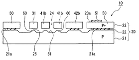
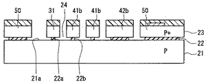
【解決手段】単結晶シリコンからなり、表面が(100)面の半導体基板の表面上に、絶縁層を介して、半導体基板よりも不純物濃度の高いP導電型のシリコンからなる半導体層が配置された基板を準備する。半導体層を異方性エッチングし、絶縁層に達する溝を形成して可動部を区画する。溝を通じて絶縁層をエッチングし、溝を半導体基板に達するものとするとともに、横方向において可動部直下における絶縁層の幅を可動部の幅よりも狭くする。上記溝を通じて半導体基板をアルカリエッチングし、突起先端が絶縁層と接する突起部を、可動部直下における半導体基板の表面に形成する。可動部直下に位置する絶縁層を除去する。
【選択図】図6
Description
エッチングストッパとなるシリコン窒化膜(絶縁層としての第3絶縁層)及びポリシリコン薄膜を堆積し、上記ポリシリコン薄膜に不純物を注入してパターニングする必要がある。すなわち、電極パターン形成のためのパターニングとは別に、凹部の形成が必要である。また、電極パターン形成後には、電極パターンを覆うように、シリコン窒化膜、シリコン酸化膜、貼り合わせ用のポリシリコン薄膜を順に形成し、半導体層とは別の単結晶シリコン基板(半導体基板)をポリシリコン薄膜の表面に貼り合わせ、半導体層と半導体基板の表裏を逆にして、半導体層側を表面研磨して所望の厚さ(例えば2〜20μm)まで薄膜化する必要がある。このように、半導体層にトレンチを形成する前に、突起部を形成するための複雑な製造工程を経るため、製造コストが増加してしまう。
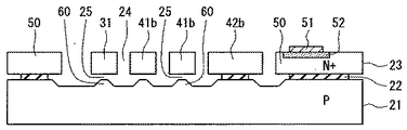
図1は、第1実施形態に係る半導体力学量センサの概略構成を示す平面図である。図2は、図1のII−II線に沿う断面図である。以下においては、便宜上、基板(若しくは半導体基板)の厚み方向を縦方向とし、厚み方向に垂直な方向を横方向とする。
るので、オーミックコンタクト用のコンタクト領域を半導体層23の表面23a側表層に形成しなくとも良い。
に示したように、半導体基板21よりも不純物濃度の高いP導電型(P+)のシリコンからなる半導体層23を採用すると、高濃度P導電型(P+)の半導体層23のエッチングを抑制しつつ、半導体層23よりも低濃度の半導体基板21を選択的にエッチングして、突起部60を形成することができる。
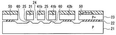
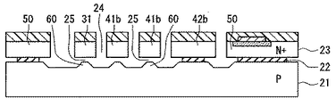
次に、本発明の第2実施形態を、図15及び図16に基づいて説明する。図15及び図16は、第2実施形態に係る半導体力学量センサの製造方法を示す断面図である。
のエッチングを実施しない。したがって、半導体基板21の主面の面方位、換言すれば、溝24bの半導体基板21における部分の面方位によっては、横方向のうちの、錘部32の長手方向及び該長手方向に垂直な短手方向の一方で、突起部60の突起先端の幅が、直上の位置する梁の幅とほぼ一致することもありえる。しかしながら、長手方向及び短手方向の他方では、突起部60の突起先端の幅が、直上の位置する梁の幅よりも狭くなるため、突起部60の機能としては問題ない。
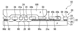
次に、本発明の第3実施形態を、図17〜図22に基づいて説明する。図17は、第3実施形態に係る半導体力学量センサの概略構成を示す断面図である。図18〜図22は、図17に示す半導体力学量センサの製造方法を示す断面図である。
層全域にN導電型不純物を導入しても良い。
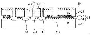
次に、本発明の第4実施形態を、図23〜図29に基づいて説明する。図23は、第4実施形態に係る半導体力学量センサの概略構成を示す平面図である。図24は、図23のXXIV−XXIV線に沿う断面図である。図25は、図23の突起部周辺を拡大した図である。図26は、製造方法を説明する上で、便宜上、図23〜図25に示す半導体力学量センサを簡素化した構成の断面図である。図27〜図29は、第4実施形態に係る半導体力学量センサの製造方法を示す断面図である。
30に対して突起部60を位置精度良く形成し、且つ、製造コストを低減することができる。
、固定部40a,40bの固定電極41a,41b直下のみに位置している。そして、両突起部60a,60bは、電気的に分離されている。また、突起部60aは、その端部が、下部配線90aの端部と一体的に連結されている。なお、図32に示す例では、片持ち梁構造の固定電極41a,41bの直下にも、突起部60bを形成しているが、固定電極41a,41bは、梁の質量が、可動部30の質量よりも小さく、縦方向において可動部30よりも撓みにくい(変位しにくい)ので、突起部60aのみを形成した構成としても良い。図32は、半導体力学量センサの変形例を示す平面図であり、図23に対応している。
21・・・半導体基板
22・・・絶縁層
23・・・半導体層
24・・・貫通孔
24a・・・溝
30・・・可動部
31・・・可動電極
40a,40b・・・固定部
41a,41b・・・固定電極
60・・・突起部
61・・・凹部
Claims (9)
- 絶縁層を介して半導体基板上に配置された半導体層に、力学量の印加に応じて所定方向に変位可能な可動部としての梁構造体を構成するとともに、前記半導体層と前記半導体基板との間に下部配線を形成してなる半導体力学量センサの製造方法であって、
前記絶縁層として、前記半導体基板の一面上に配置された第1絶縁層と、前記第1絶縁層上に配置された第2絶縁層を含み、
前記半導体基板の一面上に、前記第1絶縁層を介して導電層を形成し、該導電層をパターニングして、前記半導体基板の厚み方向に垂直な方向において、前記下部配線とは異なる位置にあって前記可動部を構成する梁を横切る突起部を、前記下部配線とともに形成する工程と、
前記突起部を覆うように、前記導電層上に前記第2絶縁層を形成する工程と、
前記第2絶縁層を介して、前記半導体層を形成する工程と、
前記半導体層における前記第2絶縁層とは反対の表面側から前記半導体層を異方性エッチングし、前記第2絶縁層に達する溝を形成して、前記半導体層に前記可動部を区画する工程と、
前記溝を通じて前記第2絶縁層をエッチングし、前記可動部直下に位置する前記第2絶縁層を除去する工程と、を備えることを特徴とする半導体力学量センサの製造方法。 - 前記梁の短手側の両端を横切るように、前記突起部を形成することを特徴とする請求項1に記載の半導体力学量センサの製造方法。
- 前記可動部は、少なくとも一部が互いに平行配置された複数の梁を有し、
前記複数の梁の短手側の両端を、互いに平行な部分でまとめて横切るように、前記突起部を形成することを特徴とする請求項2に記載の半導体力学量センサの製造方法。 - 前記絶縁層として、前記第1絶縁層と前記第2絶縁層の間に配置され、前記第2絶縁層をエッチングする際のストッパとなる第3絶縁層を含み、
前記第1絶縁層及び前記第3絶縁層を介して、前記半導体基板の一面上に、前記導電層を形成することを特徴とする請求項1〜3いずれか1項に記載の半導体力学量センサの製造方法。 - 絶縁層を介して半導体基板上に配置された半導体層に、力学量の印加に応じて所定方向に変位可能な可動部が梁構造体として構成されるとともに、前記半導体層と前記半導体基板との間に下部配線が形成された半導体力学量センサであって、
前記絶縁層として、前記半導体基板の一面上に配置された第1絶縁層と、前記第1絶縁層上に配置された第2絶縁層を含み、
前記半導体基板の一面には、前記第1絶縁層介して、前記下部配線が配置されるとともに、前記下部配線と同一の導電材料からなり、前記半導体基板の厚み方向に垂直な方向において前記可動部を構成する梁を横切る突起部が、前記下部配線と異なる位置に配置され、
前記半導体層には、前記半導体基板の厚み方向に延びて貫通する貫通孔が形成され、該貫通孔により前記半導体層に前記可動部が区画されており、
前記可動部と前記突起部との対向領域には、該対向領域における前記第2絶縁層の除去により、前記貫通孔と連なる空洞部が形成されていることを特徴とする半導体力学量センサ。 - 前記突起部は、前記梁の短手側の両端を横切って形成されていることを特徴とする請求項5に記載の半導体力学量センサ。
- 前記可動部は、少なくとも一部が互いに平行配置された複数の梁を有し、
前記突起部は、前記複数の梁の短手側の両端を、互いに平行な部分でまとめて横切って形成されていることを特徴とする請求項6に記載の半導体力学量センサ。 - 前記突起部が、前記可動部と電気的に接続されていることを特徴とする請求項7に記載の半導体力学量センサ。
- 前記絶縁層として、前記第1絶縁層と前記第2絶縁層の間に配置され、前記第2絶縁層をエッチングする際のストッパとなる第3絶縁層を含み、
前記下部配線及び前記突起部は、前記第3絶縁層上に形成されていることを特徴とする請求項5〜8いずれか1項に記載の半導体力学量センサ。
Priority Applications (1)
| Application Number | Priority Date | Filing Date | Title |
|---|---|---|---|
| JP2013080452A JP5494861B2 (ja) | 2009-06-09 | 2013-04-08 | 半導体力学量センサの製造方法及び半導体力学量センサ |
Applications Claiming Priority (3)
| Application Number | Priority Date | Filing Date | Title |
|---|---|---|---|
| JP2009138494 | 2009-06-09 | ||
| JP2009138494 | 2009-06-09 | ||
| JP2013080452A JP5494861B2 (ja) | 2009-06-09 | 2013-04-08 | 半導体力学量センサの製造方法及び半導体力学量センサ |
Related Parent Applications (1)
| Application Number | Title | Priority Date | Filing Date |
|---|---|---|---|
| JP2010121888A Division JP5316479B2 (ja) | 2009-06-09 | 2010-05-27 | 半導体力学量センサの製造方法及び半導体力学量センサ |
Publications (2)
| Publication Number | Publication Date |
|---|---|
| JP2013178255A true JP2013178255A (ja) | 2013-09-09 |
| JP5494861B2 JP5494861B2 (ja) | 2014-05-21 |
Family
ID=43299767
Family Applications (2)
| Application Number | Title | Priority Date | Filing Date |
|---|---|---|---|
| JP2010121888A Expired - Fee Related JP5316479B2 (ja) | 2009-06-09 | 2010-05-27 | 半導体力学量センサの製造方法及び半導体力学量センサ |
| JP2013080452A Expired - Fee Related JP5494861B2 (ja) | 2009-06-09 | 2013-04-08 | 半導体力学量センサの製造方法及び半導体力学量センサ |
Family Applications Before (1)
| Application Number | Title | Priority Date | Filing Date |
|---|---|---|---|
| JP2010121888A Expired - Fee Related JP5316479B2 (ja) | 2009-06-09 | 2010-05-27 | 半導体力学量センサの製造方法及び半導体力学量センサ |
Country Status (2)
| Country | Link |
|---|---|
| US (1) | US8413507B2 (ja) |
| JP (2) | JP5316479B2 (ja) |
Cited By (1)
| Publication number | Priority date | Publication date | Assignee | Title |
|---|---|---|---|---|
| JP2015160293A (ja) * | 2014-02-28 | 2015-09-07 | セイコーエプソン株式会社 | ウェハレベル封止構造及びmems素子の製造方法 |
Families Citing this family (25)
| Publication number | Priority date | Publication date | Assignee | Title |
|---|---|---|---|---|
| JP5115618B2 (ja) * | 2009-12-17 | 2013-01-09 | 株式会社デンソー | 半導体装置 |
| DE102010029708B4 (de) * | 2010-06-04 | 2023-03-02 | Robert Bosch Gmbh | Mikromechanisches System |
| DE102010038461B4 (de) * | 2010-07-27 | 2018-05-30 | Robert Bosch Gmbh | Drehratensensor und Verfahren zur Herstellung eines Masseelements |
| TWI434802B (zh) * | 2010-12-23 | 2014-04-21 | Ind Tech Res Inst | 具電性絕緣結構之微機電裝置及其製造方法 |
| CN102156203B (zh) | 2011-03-15 | 2013-07-24 | 迈尔森电子(天津)有限公司 | Mems惯性传感器及其形成方法 |
| US8852984B1 (en) | 2011-03-30 | 2014-10-07 | Silicon Laboratories | Technique for forming a MEMS device |
| US8877536B1 (en) * | 2011-03-30 | 2014-11-04 | Silicon Laboratories Inc. | Technique for forming a MEMS device using island structures |
| JP5790429B2 (ja) * | 2011-11-17 | 2015-10-07 | セイコーエプソン株式会社 | 物理量センサー素子、物理量センサー素子の製造方法及び電子機器 |
| JP6035733B2 (ja) * | 2011-12-19 | 2016-11-30 | セイコーエプソン株式会社 | 物理量センサーの製造方法 |
| TWI469254B (zh) | 2011-12-29 | 2015-01-11 | Ind Tech Res Inst | 具多重電性通道的微機電裝置及其製作方法 |
| JP6295435B2 (ja) * | 2013-02-06 | 2018-03-20 | パナソニックIpマネジメント株式会社 | Memsデバイス |
| GB2521990A (en) * | 2013-03-22 | 2015-07-15 | Schrader Electronics Ltd | A microelectromechanical switch and related fabrication method |
| WO2014181518A1 (ja) * | 2013-05-09 | 2014-11-13 | 株式会社デンソー | Soi基板、物理量センサ、soi基板の製造方法、および物理量センサの製造方法 |
| JP6020341B2 (ja) * | 2013-05-09 | 2016-11-02 | 株式会社デンソー | 容量式物理量センサおよびその製造方法 |
| JP2015010871A (ja) * | 2013-06-27 | 2015-01-19 | 株式会社デンソー | 物理量センサ |
| JP6020392B2 (ja) * | 2013-09-03 | 2016-11-02 | 株式会社デンソー | 加速度センサ |
| JP6160823B2 (ja) * | 2013-09-10 | 2017-07-12 | セイコーエプソン株式会社 | 物理量センサー、振動デバイス、電子機器および移動体 |
| JP6409351B2 (ja) | 2014-06-12 | 2018-10-24 | 株式会社デンソー | 物理量センサ |
| US11313796B2 (en) | 2017-03-06 | 2022-04-26 | Asahi Kasei Microdevices Corporation | Optical waveguide and optical concentration measuring apparatus comprising a support with a shifted connecting portion |
| JP2019120559A (ja) * | 2017-12-28 | 2019-07-22 | セイコーエプソン株式会社 | 物理量センサー、物理量センサーの製造方法、物理量センサーデバイス、電子機器および移動体 |
| US10928318B2 (en) | 2018-08-31 | 2021-02-23 | Asahi Kasei Microdevices Corporation | Optical waveguide and optical concentration measuring apparatus |
| JP7537124B2 (ja) * | 2020-04-28 | 2024-08-21 | セイコーエプソン株式会社 | 物理量センサー、電子機器および移動体 |
| DE102020214925A1 (de) | 2020-11-27 | 2022-06-02 | Robert Bosch Gesellschaft mit beschränkter Haftung | Verfahren zur Herstellung eines Polysilizium-SOI-Substrats mit einer Kavität |
| CN112194097B (zh) * | 2020-12-07 | 2021-05-07 | 中芯集成电路制造(绍兴)有限公司 | 一种惯性传感器及其形成方法 |
| US11545577B2 (en) * | 2020-12-08 | 2023-01-03 | Globalfoundries U.S. Inc. | Semiconductor structure with in-device high resistivity polycrystalline semiconductor element and method |
Citations (6)
| Publication number | Priority date | Publication date | Assignee | Title |
|---|---|---|---|---|
| JPH08320339A (ja) * | 1995-05-25 | 1996-12-03 | Nippondenso Co Ltd | 半導体力学量センサ |
| JPH09127151A (ja) * | 1995-11-01 | 1997-05-16 | Murata Mfg Co Ltd | 加速度センサ |
| JPH10261806A (ja) * | 1997-03-21 | 1998-09-29 | Nissan Motor Co Ltd | 微小機械およびその製造方法 |
| JPH11230985A (ja) * | 1998-02-18 | 1999-08-27 | Denso Corp | 半導体力学量センサ |
| JP2001091263A (ja) * | 1999-09-22 | 2001-04-06 | Toyota Motor Corp | 半導体センサ及び同半導体センサの製造方法 |
| JP2002036198A (ja) * | 2000-05-17 | 2002-02-05 | Robert Bosch Gmbh | マイクロメカニック構成素子及びその製造方法 |
Family Cites Families (27)
| Publication number | Priority date | Publication date | Assignee | Title |
|---|---|---|---|---|
| JPS62266876A (ja) | 1986-05-14 | 1987-11-19 | Nippon Denso Co Ltd | 半導体圧力センサ |
| US5605598A (en) * | 1990-10-17 | 1997-02-25 | The Charles Stark Draper Laboratory Inc. | Monolithic micromechanical vibrating beam accelerometer with trimmable resonant frequency |
| JPH04240776A (ja) * | 1991-01-24 | 1992-08-28 | Toshiba Corp | 半導体圧力センサおよびその製造方法 |
| JPH05335596A (ja) * | 1991-02-25 | 1993-12-17 | Nissan Motor Co Ltd | 半導体加速度センサおよびその製造方法 |
| JPH04286165A (ja) | 1991-03-15 | 1992-10-12 | Ricoh Co Ltd | 微小機械及びその製造方法 |
| US5198390A (en) | 1992-01-16 | 1993-03-30 | Cornell Research Foundation, Inc. | RIE process for fabricating submicron, silicon electromechanical structures |
| US5549785A (en) * | 1992-09-14 | 1996-08-27 | Nippondenso Co., Ltd. | Method of producing a semiconductor dynamic sensor |
| JPH06213924A (ja) | 1993-01-13 | 1994-08-05 | Hitachi Ltd | トランスジューサ、これを利用したマイクロセンサ、車両制御システム |
| ATE269588T1 (de) | 1993-02-04 | 2004-07-15 | Cornell Res Foundation Inc | Mikrostrukturen und einzelmask, einkristall- herstellungsverfahren |
| JP3189506B2 (ja) | 1993-06-07 | 2001-07-16 | 株式会社村田製作所 | 加速度センサ |
| JPH08219795A (ja) | 1995-02-10 | 1996-08-30 | Murata Mfg Co Ltd | 角速度センサ |
| JP3489273B2 (ja) | 1995-06-27 | 2004-01-19 | 株式会社デンソー | 半導体力学量センサの製造方法 |
| JPH09105760A (ja) | 1995-10-09 | 1997-04-22 | Fujikura Ltd | 加速度センサ |
| JPH09292409A (ja) * | 1996-04-26 | 1997-11-11 | Hitachi Ltd | 加速度センサ |
| JPH10135488A (ja) * | 1996-10-29 | 1998-05-22 | Murata Mfg Co Ltd | 半導体加工部品の製造方法 |
| DE19903380B4 (de) | 1998-02-02 | 2007-10-18 | Denso Corp., Kariya | Halbleitersensoren für eine physikalische Grösse und ihre Herstellungsverfahren |
| JPH11230986A (ja) * | 1998-02-18 | 1999-08-27 | Denso Corp | 半導体力学量センサ |
| US6065341A (en) | 1998-02-18 | 2000-05-23 | Denso Corporation | Semiconductor physical quantity sensor with stopper portion |
| JPH11248733A (ja) * | 1998-03-05 | 1999-09-17 | Denso Corp | 角速度センサ及びその製造方法 |
| JPH11258265A (ja) * | 1998-03-16 | 1999-09-24 | Akebono Brake Ind Co Ltd | 半導体加速度センサ及びその製造方法 |
| JP2001091262A (ja) * | 1999-09-21 | 2001-04-06 | Toyota Motor Corp | 半導体センサの製造方法、及び半導体センサ |
| JP4075470B2 (ja) * | 2002-05-31 | 2008-04-16 | 株式会社豊田中央研究所 | センサ装置 |
| JP4254220B2 (ja) * | 2002-11-29 | 2009-04-15 | 株式会社デンソー | 電磁アクチュエータおよび力学量センサ |
| US7094622B1 (en) * | 2003-08-27 | 2006-08-22 | Louisiana Tech University Foundation, Inc. | Polymer based tunneling sensor |
| KR100599124B1 (ko) * | 2005-02-14 | 2006-07-12 | 삼성전자주식회사 | 부유 구조체 제조방법 |
| JP2008008672A (ja) | 2006-06-27 | 2008-01-17 | Matsushita Electric Works Ltd | 加速度センサ |
| JP2008264902A (ja) | 2007-04-17 | 2008-11-06 | Toyota Motor Corp | シリコン構造体とシリコン構造体の製造方法 |
-
2010
- 2010-05-27 JP JP2010121888A patent/JP5316479B2/ja not_active Expired - Fee Related
- 2010-06-08 US US12/801,405 patent/US8413507B2/en not_active Expired - Fee Related
-
2013
- 2013-04-08 JP JP2013080452A patent/JP5494861B2/ja not_active Expired - Fee Related
Patent Citations (6)
| Publication number | Priority date | Publication date | Assignee | Title |
|---|---|---|---|---|
| JPH08320339A (ja) * | 1995-05-25 | 1996-12-03 | Nippondenso Co Ltd | 半導体力学量センサ |
| JPH09127151A (ja) * | 1995-11-01 | 1997-05-16 | Murata Mfg Co Ltd | 加速度センサ |
| JPH10261806A (ja) * | 1997-03-21 | 1998-09-29 | Nissan Motor Co Ltd | 微小機械およびその製造方法 |
| JPH11230985A (ja) * | 1998-02-18 | 1999-08-27 | Denso Corp | 半導体力学量センサ |
| JP2001091263A (ja) * | 1999-09-22 | 2001-04-06 | Toyota Motor Corp | 半導体センサ及び同半導体センサの製造方法 |
| JP2002036198A (ja) * | 2000-05-17 | 2002-02-05 | Robert Bosch Gmbh | マイクロメカニック構成素子及びその製造方法 |
Cited By (1)
| Publication number | Priority date | Publication date | Assignee | Title |
|---|---|---|---|---|
| JP2015160293A (ja) * | 2014-02-28 | 2015-09-07 | セイコーエプソン株式会社 | ウェハレベル封止構造及びmems素子の製造方法 |
Also Published As
| Publication number | Publication date |
|---|---|
| JP5316479B2 (ja) | 2013-10-16 |
| US8413507B2 (en) | 2013-04-09 |
| JP5494861B2 (ja) | 2014-05-21 |
| JP2011017693A (ja) | 2011-01-27 |
| US20100307246A1 (en) | 2010-12-09 |
Similar Documents
| Publication | Publication Date | Title |
|---|---|---|
| JP5494861B2 (ja) | 半導体力学量センサの製造方法及び半導体力学量センサ | |
| US6951824B2 (en) | Method for manufacturing a micromechanical component and a component that is manufactured in accordance with the method | |
| US6291875B1 (en) | Microfabricated structures with electrical isolation and interconnections | |
| US9194882B2 (en) | Inertial and pressure sensors on single chip | |
| US9908771B2 (en) | Inertial and pressure sensors on single chip | |
| US20100162823A1 (en) | Mems sensor and mems sensor manufacture method | |
| KR20120139744A (ko) | Mems 마이크로폰 및 그 제조 방법 | |
| JP2009150863A (ja) | 多層シリコン・オン・インシュレータ基板中に位置非依存の駆動装置電極を有するセンサ | |
| JP2005243576A (ja) | マイクロスイッチング素子製造方法およびマイクロスイッチング素子 | |
| US5930595A (en) | Isolation process for surface micromachined sensors and actuators | |
| JP2009016717A (ja) | 半導体装置およびその製造方法 | |
| US6846724B2 (en) | Method for fabricating a microelectromechanical system (MEMS) device using a pre-patterned bridge | |
| TW201524889A (zh) | 微機械構件與製造微機械構件的方法 | |
| US6469330B1 (en) | Process for manufacturing integrated devices comprising microstructures and associated suspended electrical interconnections | |
| CN102530837B (zh) | 用于制造微机械组件的方法 | |
| US11150092B2 (en) | Sensor | |
| KR20000028948A (ko) | 각속도 센서 제조방법 | |
| JP2004347475A (ja) | 容量式力学量センサ | |
| EP1770056B1 (en) | Method for manufacturing a micro-electro-mechanical structure | |
| JP5167652B2 (ja) | Mems素子 | |
| US7371601B2 (en) | Piezoresistive sensing structure | |
| JP6032046B2 (ja) | 半導体装置およびその製造方法 | |
| JP3725059B2 (ja) | 半導体力学量センサ | |
| JP3725078B2 (ja) | 半導体力学量センサの製造方法 | |
| JP2008157969A (ja) | 半導体力学量センサおよび半導体力学量センサの製造方法 |
Legal Events
| Date | Code | Title | Description |
|---|---|---|---|
| A977 | Report on retrieval |
Free format text: JAPANESE INTERMEDIATE CODE: A971007 Effective date: 20140114 |
|
| TRDD | Decision of grant or rejection written | ||
| A01 | Written decision to grant a patent or to grant a registration (utility model) |
Free format text: JAPANESE INTERMEDIATE CODE: A01 Effective date: 20140204 |
|
| A61 | First payment of annual fees (during grant procedure) |
Free format text: JAPANESE INTERMEDIATE CODE: A61 Effective date: 20140217 |
|
| R151 | Written notification of patent or utility model registration |
Ref document number: 5494861 Country of ref document: JP Free format text: JAPANESE INTERMEDIATE CODE: R151 |
|
| R250 | Receipt of annual fees |
Free format text: JAPANESE INTERMEDIATE CODE: R250 |
|
| R250 | Receipt of annual fees |
Free format text: JAPANESE INTERMEDIATE CODE: R250 |
|
| R250 | Receipt of annual fees |
Free format text: JAPANESE INTERMEDIATE CODE: R250 |
|
| R250 | Receipt of annual fees |
Free format text: JAPANESE INTERMEDIATE CODE: R250 |
|
| LAPS | Cancellation because of no payment of annual fees |