JP5648191B2 - 高電圧垂直トランジスタのためのセグメントピラーレイアウト - Google Patents
高電圧垂直トランジスタのためのセグメントピラーレイアウト Download PDFInfo
- Publication number
- JP5648191B2 JP5648191B2 JP2013022107A JP2013022107A JP5648191B2 JP 5648191 B2 JP5648191 B2 JP 5648191B2 JP 2013022107 A JP2013022107 A JP 2013022107A JP 2013022107 A JP2013022107 A JP 2013022107A JP 5648191 B2 JP5648191 B2 JP 5648191B2
- Authority
- JP
- Japan
- Prior art keywords
- section
- transistor
- region
- pillar
- pillars
- Prior art date
- Legal status (The legal status is an assumption and is not a legal conclusion. Google has not performed a legal analysis and makes no representation as to the accuracy of the status listed.)
- Expired - Fee Related
Links
Images




Classifications
-
- H—ELECTRICITY
- H10—SEMICONDUCTOR DEVICES; ELECTRIC SOLID-STATE DEVICES NOT OTHERWISE PROVIDED FOR
- H10D—INORGANIC ELECTRIC SEMICONDUCTOR DEVICES
- H10D30/00—Field-effect transistors [FET]
- H10D30/60—Insulated-gate field-effect transistors [IGFET]
- H10D30/64—Double-diffused metal-oxide semiconductor [DMOS] FETs
- H10D30/66—Vertical DMOS [VDMOS] FETs
- H10D30/668—Vertical DMOS [VDMOS] FETs having trench gate electrodes, e.g. UMOS transistors
-
- H—ELECTRICITY
- H10—SEMICONDUCTOR DEVICES; ELECTRIC SOLID-STATE DEVICES NOT OTHERWISE PROVIDED FOR
- H10D—INORGANIC ELECTRIC SEMICONDUCTOR DEVICES
- H10D62/00—Semiconductor bodies, or regions thereof, of devices having potential barriers
- H10D62/10—Shapes, relative sizes or dispositions of the regions of the semiconductor bodies; Shapes of the semiconductor bodies
- H10D62/102—Constructional design considerations for preventing surface leakage or controlling electric field concentration
-
- H—ELECTRICITY
- H10—SEMICONDUCTOR DEVICES; ELECTRIC SOLID-STATE DEVICES NOT OTHERWISE PROVIDED FOR
- H10D—INORGANIC ELECTRIC SEMICONDUCTOR DEVICES
- H10D62/00—Semiconductor bodies, or regions thereof, of devices having potential barriers
- H10D62/10—Shapes, relative sizes or dispositions of the regions of the semiconductor bodies; Shapes of the semiconductor bodies
- H10D62/124—Shapes, relative sizes or dispositions of the regions of semiconductor bodies or of junctions between the regions
- H10D62/126—Top-view geometrical layouts of the regions or the junctions
- H10D62/127—Top-view geometrical layouts of the regions or the junctions of cellular field-effect devices, e.g. multicellular DMOS transistors or IGBTs
-
- H—ELECTRICITY
- H10—SEMICONDUCTOR DEVICES; ELECTRIC SOLID-STATE DEVICES NOT OTHERWISE PROVIDED FOR
- H10D—INORGANIC ELECTRIC SEMICONDUCTOR DEVICES
- H10D64/00—Electrodes of devices having potential barriers
- H10D64/111—Field plates
- H10D64/117—Recessed field plates, e.g. trench field plates or buried field plates
-
- H—ELECTRICITY
- H10—SEMICONDUCTOR DEVICES; ELECTRIC SOLID-STATE DEVICES NOT OTHERWISE PROVIDED FOR
- H10D—INORGANIC ELECTRIC SEMICONDUCTOR DEVICES
- H10D64/00—Electrodes of devices having potential barriers
- H10D64/20—Electrodes characterised by their shapes, relative sizes or dispositions
- H10D64/27—Electrodes not carrying the current to be rectified, amplified, oscillated or switched, e.g. gates
- H10D64/311—Gate electrodes for field-effect devices
- H10D64/411—Gate electrodes for field-effect devices for FETs
- H10D64/511—Gate electrodes for field-effect devices for FETs for IGFETs
- H10D64/517—Gate electrodes for field-effect devices for FETs for IGFETs characterised by the conducting layers
- H10D64/519—Gate electrodes for field-effect devices for FETs for IGFETs characterised by the conducting layers characterised by their top-view geometrical layouts
-
- H—ELECTRICITY
- H10—SEMICONDUCTOR DEVICES; ELECTRIC SOLID-STATE DEVICES NOT OTHERWISE PROVIDED FOR
- H10D—INORGANIC ELECTRIC SEMICONDUCTOR DEVICES
- H10D84/00—Integrated devices formed in or on semiconductor substrates that comprise only semiconducting layers, e.g. on Si wafers or on GaAs-on-Si wafers
- H10D84/80—Integrated devices formed in or on semiconductor substrates that comprise only semiconducting layers, e.g. on Si wafers or on GaAs-on-Si wafers characterised by the integration of at least one component covered by groups H10D12/00 or H10D30/00, e.g. integration of IGFETs
- H10D84/82—Integrated devices formed in or on semiconductor substrates that comprise only semiconducting layers, e.g. on Si wafers or on GaAs-on-Si wafers characterised by the integration of at least one component covered by groups H10D12/00 or H10D30/00, e.g. integration of IGFETs of only field-effect components
- H10D84/83—Integrated devices formed in or on semiconductor substrates that comprise only semiconducting layers, e.g. on Si wafers or on GaAs-on-Si wafers characterised by the integration of at least one component covered by groups H10D12/00 or H10D30/00, e.g. integration of IGFETs of only field-effect components of only insulated-gate FETs [IGFET]
-
- H—ELECTRICITY
- H10—SEMICONDUCTOR DEVICES; ELECTRIC SOLID-STATE DEVICES NOT OTHERWISE PROVIDED FOR
- H10D—INORGANIC ELECTRIC SEMICONDUCTOR DEVICES
- H10D84/00—Integrated devices formed in or on semiconductor substrates that comprise only semiconducting layers, e.g. on Si wafers or on GaAs-on-Si wafers
- H10D84/80—Integrated devices formed in or on semiconductor substrates that comprise only semiconducting layers, e.g. on Si wafers or on GaAs-on-Si wafers characterised by the integration of at least one component covered by groups H10D12/00 or H10D30/00, e.g. integration of IGFETs
- H10D84/82—Integrated devices formed in or on semiconductor substrates that comprise only semiconducting layers, e.g. on Si wafers or on GaAs-on-Si wafers characterised by the integration of at least one component covered by groups H10D12/00 or H10D30/00, e.g. integration of IGFETs of only field-effect components
- H10D84/83—Integrated devices formed in or on semiconductor substrates that comprise only semiconducting layers, e.g. on Si wafers or on GaAs-on-Si wafers characterised by the integration of at least one component covered by groups H10D12/00 or H10D30/00, e.g. integration of IGFETs of only field-effect components of only insulated-gate FETs [IGFET]
- H10D84/836—Integrated devices formed in or on semiconductor substrates that comprise only semiconducting layers, e.g. on Si wafers or on GaAs-on-Si wafers characterised by the integration of at least one component covered by groups H10D12/00 or H10D30/00, e.g. integration of IGFETs of only field-effect components of only insulated-gate FETs [IGFET] comprising EDMOS
-
- H—ELECTRICITY
- H10—SEMICONDUCTOR DEVICES; ELECTRIC SOLID-STATE DEVICES NOT OTHERWISE PROVIDED FOR
- H10D—INORGANIC ELECTRIC SEMICONDUCTOR DEVICES
- H10D84/00—Integrated devices formed in or on semiconductor substrates that comprise only semiconducting layers, e.g. on Si wafers or on GaAs-on-Si wafers
- H10D84/80—Integrated devices formed in or on semiconductor substrates that comprise only semiconducting layers, e.g. on Si wafers or on GaAs-on-Si wafers characterised by the integration of at least one component covered by groups H10D12/00 or H10D30/00, e.g. integration of IGFETs
- H10D84/82—Integrated devices formed in or on semiconductor substrates that comprise only semiconducting layers, e.g. on Si wafers or on GaAs-on-Si wafers characterised by the integration of at least one component covered by groups H10D12/00 or H10D30/00, e.g. integration of IGFETs of only field-effect components
- H10D84/83—Integrated devices formed in or on semiconductor substrates that comprise only semiconducting layers, e.g. on Si wafers or on GaAs-on-Si wafers characterised by the integration of at least one component covered by groups H10D12/00 or H10D30/00, e.g. integration of IGFETs of only field-effect components of only insulated-gate FETs [IGFET]
- H10D84/837—Integrated devices formed in or on semiconductor substrates that comprise only semiconducting layers, e.g. on Si wafers or on GaAs-on-Si wafers characterised by the integration of at least one component covered by groups H10D12/00 or H10D30/00, e.g. integration of IGFETs of only field-effect components of only insulated-gate FETs [IGFET] comprising vertical IGFETs
- H10D84/839—Integrated devices formed in or on semiconductor substrates that comprise only semiconducting layers, e.g. on Si wafers or on GaAs-on-Si wafers characterised by the integration of at least one component covered by groups H10D12/00 or H10D30/00, e.g. integration of IGFETs of only field-effect components of only insulated-gate FETs [IGFET] comprising vertical IGFETs comprising VDMOS
-
- H—ELECTRICITY
- H10—SEMICONDUCTOR DEVICES; ELECTRIC SOLID-STATE DEVICES NOT OTHERWISE PROVIDED FOR
- H10W—GENERIC PACKAGES, INTERCONNECTIONS, CONNECTORS OR OTHER CONSTRUCTIONAL DETAILS OF DEVICES COVERED BY CLASS H10
- H10W42/00—Arrangements for protection of devices
- H10W42/121—Arrangements for protection of devices protecting against mechanical damage
-
- H—ELECTRICITY
- H10—SEMICONDUCTOR DEVICES; ELECTRIC SOLID-STATE DEVICES NOT OTHERWISE PROVIDED FOR
- H10D—INORGANIC ELECTRIC SEMICONDUCTOR DEVICES
- H10D62/00—Semiconductor bodies, or regions thereof, of devices having potential barriers
- H10D62/10—Shapes, relative sizes or dispositions of the regions of the semiconductor bodies; Shapes of the semiconductor bodies
- H10D62/13—Semiconductor regions connected to electrodes carrying current to be rectified, amplified or switched, e.g. source or drain regions
- H10D62/149—Source or drain regions of field-effect devices
- H10D62/151—Source or drain regions of field-effect devices of IGFETs
- H10D62/156—Drain regions of DMOS transistors
- H10D62/157—Impurity concentrations or distributions
-
- H—ELECTRICITY
- H10—SEMICONDUCTOR DEVICES; ELECTRIC SOLID-STATE DEVICES NOT OTHERWISE PROVIDED FOR
- H10D—INORGANIC ELECTRIC SEMICONDUCTOR DEVICES
- H10D64/00—Electrodes of devices having potential barriers
- H10D64/20—Electrodes characterised by their shapes, relative sizes or dispositions
- H10D64/27—Electrodes not carrying the current to be rectified, amplified, oscillated or switched, e.g. gates
- H10D64/311—Gate electrodes for field-effect devices
- H10D64/411—Gate electrodes for field-effect devices for FETs
- H10D64/511—Gate electrodes for field-effect devices for FETs for IGFETs
- H10D64/512—Disposition of the gate electrodes, e.g. buried gates
- H10D64/513—Disposition of the gate electrodes, e.g. buried gates within recesses in the substrate, e.g. trench gates, groove gates or buried gates
-
- H—ELECTRICITY
- H10—SEMICONDUCTOR DEVICES; ELECTRIC SOLID-STATE DEVICES NOT OTHERWISE PROVIDED FOR
- H10D—INORGANIC ELECTRIC SEMICONDUCTOR DEVICES
- H10D84/00—Integrated devices formed in or on semiconductor substrates that comprise only semiconducting layers, e.g. on Si wafers or on GaAs-on-Si wafers
- H10D84/01—Manufacture or treatment
Landscapes
- Insulated Gate Type Field-Effect Transistor (AREA)
- Thin Film Transistor (AREA)
- Junction Field-Effect Transistors (AREA)
- Electrodes Of Semiconductors (AREA)
- Metal-Oxide And Bipolar Metal-Oxide Semiconductor Integrated Circuits (AREA)
Description
前記トランジスタセグメントの各々が、
前記ダイを通って垂直方向に延びる拡張したドレイン領域を含む半導体材料のピラーと、
前記ピラーの対向する側にそれぞれ配置された第1の誘電領域及び第2の誘電領域と、を含み、
前記第1の誘電領域は横方向において前記ピラーにより囲まれ、前記第2の誘電領域は横方向において前記ピラーを囲み、
さらに、前記トランジスタセグメントの各々は、
前記第1の誘電領域及び前記第2の誘電領域のそれぞれに配置された第1のフィールドプレート及び第2のフィールドプレートと、を含み、
前記複数のトランジスタセグメントは、複数のセクションに分けられており、
該複数のセクションにおける第1のセクションは、前記第2の横方向において並列関係に配置されたトランジスタセグメントの第1の行を含み、
前記複数のセクションにおける第2のセクションは、前記第2の横方向において並列関係に配置されたトランジスタセグメントの第2の行を含む、ことを特徴とする。
前記トランジスタセグメントの各々が、
前記ダイを通って垂直方向に延びる拡張したドレイン領域を含む半導体材料のピラーと、
前記ピラーの対向する側にそれぞれ配置された第1の誘電領域及び第2の誘電領域と、を含み、
前記第1の誘電領域は横方向において前記ピラーにより囲まれ、前記第2の誘電領域は横方向において前記ピラーを囲み、
さらに、前記トランジスタセグメントの各々は、
前記第1の誘電領域及び前記第2の誘電領域のそれぞれに配置された第1のフィールドプレート及び第2のフィールドプレートと、を含み、
前記複数のトランジスタセグメントは、複数のセクションに分けられており、
第1のセクションにおけるトランジスタセグメントは、第2のセクションにおけるトランジスタセグメントに対して前記第1の横方向においてシフトされ、
前記第1のセクションの行における前記トランジスタセグメントの各々は、前記第2のセクションにおける1対のトランジスタセグメントにより分離されており、該1対のトランジスタセグメントは、端と端とが接した関係により配置されており、
前記第1のセクション及び前記第2のセクションにおける前記トランジスタセグメントのうち交互に選択されたトランジスタセグメントの前記第2の誘電領域が併合されている、ことを特徴とする。
該半導体ダイを実質的に覆うように設けられた複数のトランジスタセグメントであって、各々が第1の横方向に延びる長さ及び第2の横方向に延びる幅を有し、かつ、前記長さが前記幅の少なくとも20倍以上の大きさとなっている、複数のトランジスタセグメントと、を具備し、
前記トランジスタセグメントの各々が、
前記半導体ダイを通って垂直方向に延びる拡張したドレイン領域を含む半導体材料のピラーであって、前記第1の横方向及び前記第2の横方向に延びて、連続したレーストラック形状のリング又は楕円を形成するピラーと、
前記ピラーの対向する側にそれぞれ配置された第1の誘電領域及び第2の誘電領域と、を含み、
前記第1の誘電領域が横方向において前記ピラーにより囲まれ、前記第2の誘電領域が横方向において前記ピラーを囲み、
さらに、前記トランジスタセグメントの各々が、
前記第1の誘電領域及び前記第2の誘電領域のそれぞれに配置された第1のフィールドプレート及び第2のフィールドプレートと、を含み、
前記複数のトランジスタセグメントが、前記半導体ダイにおける対応するエリアに配置された2つ又はそれ以上のセクションに分割されている、ことを特徴とする。
該半導体ダイにおける第1のエリアに配置されたトランジスタセグメントの第1のセクションと、
前記半導体ダイの前記第1のエリアに隣接した第2のエリアに配置されたトランジスタセグメントの第2のセクションと、を具備し、
前記第1のセクション及び前記第2のセクションにおける前記トランジスタセグメントの各々が、
前記ダイの上面の近くに配置されたソース領域と該ソース領域の下に配置された拡張したドレイン領域とを有する、垂直方向に延びる半導体材料のピラーであって、前記第1の横方向及び前記第2の横方向に延びて、連続したレーストラック状のリング又は楕円を形成するピラーと、
該ピラーの対向する側にそれぞれ配置された第1の誘電領域及び第2の誘電領域と、を含み、
前記第1の誘電領域が横方向において前記ピラーにより囲まれ、前記第2の誘電領域が横方向において前記ピラーを囲み、
さらに、前記第1のセクション及び前記第2のセクションにおける前記トランジスタセグメントの各々は、前記第1の誘電領域及び前記第2の誘電領域のそれぞれに配置された第1のフィールドプレート及び第2のフィールドプレートと、を含み、
前記第1のセクション及び前記第2のセクションにおける隣接するトランジスタセグメントの対の前記第2のフィールドプレートが、それぞれ分離されているか、又は、部分的に合併している、ことを特徴とする。
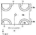
17 シリコンピラー
18a、18b ゲート部材
19a、19b フィールドプレート
21 半導体ダイ
30a 上側トランジスタセクション
30b 下側トランジスタセクション
32 ダミーシリコンピラー
Claims (11)
- 各々が、ダイ上に設けられ、第1の横方向に延びる長さ及び第2の横方向に延びる幅を備えたレーストラック形状を有する、複数のトランジスタセグメントを具備する垂直トランジスタ装置であって、
前記トランジスタセグメントの各々が、
垂直方向に延びる拡張したドレイン領域の一部を含む半導体材料のピラーと、
前記ピラーの対向する側にそれぞれ配置された第1の誘電領域及び第2の誘電領域と、
を含み、
前記第1の誘電領域は横方向において前記ピラーにより囲まれ、前記第2の誘電領域は横方向において前記ピラーを囲み、
さらに、前記トランジスタセグメントの各々は、
前記第1の誘電領域及び前記第2の誘電領域のそれぞれに配置された第1のフィールドプレート及び第2のフィールドプレートと、を含み、
前記複数のトランジスタセグメントは、複数のセクションに分けられており、
該複数のセクションにおける第1のセクションは、前記第2の横方向において並列関係に配置されたトランジスタセグメントの第1の行を含み、
前記複数のセクションにおける第2のセクションは、前記第2の横方向において並列関係に配置されたトランジスタセグメントの第2の行を含み、前記第1の行の前記トランジスタの前記ピラーが前記第2の行の前記トランジスタの前記ピラーから前記第1の横方向において分離されており、
前記第1のセクションの各トランジスタセグメントの前記第2の誘電領域が、前記第2のセクションの各トランジスタセグメントの前記第2の誘電領域と合体又は重なり合わされており、前記第1のセクションの各トランジスタセグメントの前記第2のフィールドプレートが前記第2のセクションの各トランジスタの前記第2のフィールドプレートと合体されていることを特徴とする装置。 - 前記第1のセクション及び前記第2のセクションの前記合体されるトランジスタセグメントが、前記合体されるトランジタセグメント間に位置する前記半導体材料の少なくとも1つのダミーピラー用のスペースを残している、請求項1に記載の装置。
- 前記第2の誘電領域が、前記第1の横方向の前記トランジスタの各端部に丸みのあるセクションを含んでいる、請求項1に記載の装置。
- 前記第1のフィールドプレート及び前記第2のフィールドプレートが、前記拡張したドレイン領域から完全に絶縁されており、
前記第1のフィールドプレートが横方向において前記ピラーにより囲まれ、前記第2のフィールドプレートが横方向において前記ピラーを囲む、請求項1に記載の装置。 - 前記少なくとも1つのダミーピラーが、前記第1のセクションと前記第2のセクションとを分離する単一のダミーピラーを含む、請求項2に記載の装置。
- 前記単一のダミーピラーが、前記第1の横方向において、前記第1のセクション及び前記第2のセクションにおける各トランジスタセグメントの前記第2の誘電領域の丸みのある端部に隣接する、請求項5に記載の装置。
- 前記少なくとも1つのダミーピラーが複数のダミーピラーを含み、
該複数のダミーピラーの各々が、前記第1のセクション及び前記第2のセクションにおけるトランジスタセグメントの第1及び第2の隣接するペアの丸みのある端部間の中心にそれぞれ配置されている、請求項2に記載の装置。 - 前記第1のセクション及び前記第2のセクションにおける前記トランジスタセグメントの前記長さと前記幅との比が、30〜80の範囲内にある、請求項1に記載の装置。
- 前記第1のセクション及び前記第2のセクションが、各々、前記ダイの幅の全体にわたって前記第2の横方向において延びており、前記第1のセクション及び前記第2のセクションが、連結して、前記ダイの長さの全体にわたって前記第1の横方向において延びている、請求項1に記載の装置。
- 前記ピラーが、更に、前記ダイの上面の近くに配置されたソース領域と、前記拡張したドレイン領域から前記ソース領域を垂直方向に分離するボディ領域と、を含む、請求項1に記載の装置。
- 前記ボディ領域に隣接する前記第1の誘電領域及び前記第2の誘電領域内に配置されたゲートを更に具備し、前記ゲートが、前記ボディ領域、前記第1のフィールドプレート及び前記第2のフィールドプレートから絶縁されている、請求項10に記載の装置。
Applications Claiming Priority (2)
| Application Number | Priority Date | Filing Date | Title |
|---|---|---|---|
| US11/707,406 | 2007-02-16 | ||
| US11/707,406 US7557406B2 (en) | 2007-02-16 | 2007-02-16 | Segmented pillar layout for a high-voltage vertical transistor |
Related Parent Applications (1)
| Application Number | Title | Priority Date | Filing Date |
|---|---|---|---|
| JP2008029919A Division JP2008205461A (ja) | 2007-02-16 | 2008-02-12 | 高電圧垂直トランジスタのためのセグメントピラーレイアウト |
Publications (2)
| Publication Number | Publication Date |
|---|---|
| JP2013080984A JP2013080984A (ja) | 2013-05-02 |
| JP5648191B2 true JP5648191B2 (ja) | 2015-01-07 |
Family
ID=39322673
Family Applications (3)
| Application Number | Title | Priority Date | Filing Date |
|---|---|---|---|
| JP2008029919A Pending JP2008205461A (ja) | 2007-02-16 | 2008-02-12 | 高電圧垂直トランジスタのためのセグメントピラーレイアウト |
| JP2013022106A Expired - Fee Related JP5764846B2 (ja) | 2007-02-16 | 2013-02-07 | 高電圧垂直トランジスタのためのセグメントピラーレイアウト |
| JP2013022107A Expired - Fee Related JP5648191B2 (ja) | 2007-02-16 | 2013-02-07 | 高電圧垂直トランジスタのためのセグメントピラーレイアウト |
Family Applications Before (2)
| Application Number | Title | Priority Date | Filing Date |
|---|---|---|---|
| JP2008029919A Pending JP2008205461A (ja) | 2007-02-16 | 2008-02-12 | 高電圧垂直トランジスタのためのセグメントピラーレイアウト |
| JP2013022106A Expired - Fee Related JP5764846B2 (ja) | 2007-02-16 | 2013-02-07 | 高電圧垂直トランジスタのためのセグメントピラーレイアウト |
Country Status (4)
| Country | Link |
|---|---|
| US (4) | US7557406B2 (ja) |
| EP (2) | EP1959496A3 (ja) |
| JP (3) | JP2008205461A (ja) |
| CN (2) | CN102222696B (ja) |
Families Citing this family (40)
| Publication number | Priority date | Publication date | Assignee | Title |
|---|---|---|---|---|
| US6635544B2 (en) | 2001-09-07 | 2003-10-21 | Power Intergrations, Inc. | Method of fabricating a high-voltage transistor with a multi-layered extended drain structure |
| US6573558B2 (en) * | 2001-09-07 | 2003-06-03 | Power Integrations, Inc. | High-voltage vertical transistor with a multi-layered extended drain structure |
| US7786533B2 (en) | 2001-09-07 | 2010-08-31 | Power Integrations, Inc. | High-voltage vertical transistor with edge termination structure |
| US8093621B2 (en) * | 2008-12-23 | 2012-01-10 | Power Integrations, Inc. | VTS insulated gate bipolar transistor |
| US7468536B2 (en) * | 2007-02-16 | 2008-12-23 | Power Integrations, Inc. | Gate metal routing for transistor with checkerboarded layout |
| US7859037B2 (en) * | 2007-02-16 | 2010-12-28 | Power Integrations, Inc. | Checkerboarded high-voltage vertical transistor layout |
| US7595523B2 (en) | 2007-02-16 | 2009-09-29 | Power Integrations, Inc. | Gate pullback at ends of high-voltage vertical transistor structure |
| US7557406B2 (en) * | 2007-02-16 | 2009-07-07 | Power Integrations, Inc. | Segmented pillar layout for a high-voltage vertical transistor |
| US8653583B2 (en) | 2007-02-16 | 2014-02-18 | Power Integrations, Inc. | Sensing FET integrated with a high-voltage transistor |
| US7875962B2 (en) * | 2007-10-15 | 2011-01-25 | Power Integrations, Inc. | Package for a power semiconductor device |
| US8541267B2 (en) * | 2008-03-20 | 2013-09-24 | Nxp B.V. | FinFET transistor with high-voltage capability and CMOS-compatible method for fabricating the same |
| KR101394157B1 (ko) | 2008-04-08 | 2014-05-14 | 삼성전자주식회사 | 수직 필러 트랜지스터, 이를 포함하는 디램 소자, 수직필러 트랜지스터 형성 방법 및 반도체 박막 형성 방법. |
| US7964912B2 (en) * | 2008-09-18 | 2011-06-21 | Power Integrations, Inc. | High-voltage vertical transistor with a varied width silicon pillar |
| US7871882B2 (en) * | 2008-12-20 | 2011-01-18 | Power Integrations, Inc. | Method of fabricating a deep trench insulated gate bipolar transistor |
| US20100155831A1 (en) * | 2008-12-20 | 2010-06-24 | Power Integrations, Inc. | Deep trench insulated gate bipolar transistor |
| CN101847436B (zh) * | 2009-03-24 | 2012-09-05 | 中国科学院物理研究所 | 一种基于垂直晶体管的磁性多层膜随机存储器 |
| US8115457B2 (en) | 2009-07-31 | 2012-02-14 | Power Integrations, Inc. | Method and apparatus for implementing a power converter input terminal voltage discharge circuit |
| US8207455B2 (en) * | 2009-07-31 | 2012-06-26 | Power Integrations, Inc. | Power semiconductor package with bottom surface protrusions |
| US8207577B2 (en) * | 2009-09-29 | 2012-06-26 | Power Integrations, Inc. | High-voltage transistor structure with reduced gate capacitance |
| US7893754B1 (en) | 2009-10-02 | 2011-02-22 | Power Integrations, Inc. | Temperature independent reference circuit |
| US8634218B2 (en) | 2009-10-06 | 2014-01-21 | Power Integrations, Inc. | Monolithic AC/DC converter for generating DC supply voltage |
| US8247297B2 (en) * | 2009-12-15 | 2012-08-21 | Alpha & Omega Semiconductor Inc. | Method of filling large deep trench with high quality oxide for semiconductor devices |
| US8310845B2 (en) | 2010-02-10 | 2012-11-13 | Power Integrations, Inc. | Power supply circuit with a control terminal for different functional modes of operation |
| JP5631752B2 (ja) * | 2011-01-12 | 2014-11-26 | 株式会社 日立パワーデバイス | 半導体装置および電力変換装置 |
| US8653600B2 (en) | 2012-06-01 | 2014-02-18 | Power Integrations, Inc. | High-voltage monolithic schottky device structure |
| US9455621B2 (en) | 2013-08-28 | 2016-09-27 | Power Integrations, Inc. | Controller IC with zero-crossing detector and capacitor discharge switching element |
| US9111766B2 (en) | 2013-09-24 | 2015-08-18 | Infineon Technologies Austria Ag | Transistor device with a field electrode |
| US9224854B2 (en) | 2013-10-03 | 2015-12-29 | Texas Instruments Incorporated | Trench gate trench field plate vertical MOSFET |
| US9136368B2 (en) * | 2013-10-03 | 2015-09-15 | Texas Instruments Incorporated | Trench gate trench field plate semi-vertical semi-lateral MOSFET |
| US9543396B2 (en) * | 2013-12-13 | 2017-01-10 | Power Integrations, Inc. | Vertical transistor device structure with cylindrically-shaped regions |
| US10325988B2 (en) | 2013-12-13 | 2019-06-18 | Power Integrations, Inc. | Vertical transistor device structure with cylindrically-shaped field plates |
| US9667154B2 (en) | 2015-09-18 | 2017-05-30 | Power Integrations, Inc. | Demand-controlled, low standby power linear shunt regulator |
| US9602009B1 (en) | 2015-12-08 | 2017-03-21 | Power Integrations, Inc. | Low voltage, closed loop controlled energy storage circuit |
| US9629218B1 (en) | 2015-12-28 | 2017-04-18 | Power Integrations, Inc. | Thermal protection for LED bleeder in fault condition |
| CN106298941B (zh) * | 2016-09-13 | 2019-04-09 | 上海华虹宏力半导体制造有限公司 | 屏蔽栅沟槽功率器件及其制造方法 |
| DE102018107417B4 (de) * | 2018-03-28 | 2024-02-08 | Infineon Technologies Austria Ag | Nadelzellengraben-MOSFET und Verfahren zur Herstellung desselben |
| US11031345B2 (en) * | 2018-08-14 | 2021-06-08 | Medtronic, Inc. | Integrated circuit package and method of forming same |
| JP6980626B2 (ja) * | 2018-09-18 | 2021-12-15 | 株式会社東芝 | 半導体装置 |
| US10957599B2 (en) | 2018-11-07 | 2021-03-23 | International Business Machines Corporation | Integrating extra gate VFET with single gate VFET |
| US11271100B2 (en) * | 2019-10-15 | 2022-03-08 | Infineon Technologies Austria Ag | Narrow semiconductor mesa device |
Family Cites Families (212)
| Publication number | Priority date | Publication date | Assignee | Title |
|---|---|---|---|---|
| US633065A (en) * | 1899-04-22 | 1899-09-12 | Jean Pierre Boulesque | Boat adapted to operate on land or in water. |
| JPS5712557Y2 (ja) | 1974-12-20 | 1982-03-12 | ||
| JPS53125657A (en) | 1977-04-09 | 1978-11-02 | Hoshizaki Electric Co Ltd | Detecting system for completion of deicing in automatic ice machine |
| JPS5710975Y2 (ja) | 1977-05-31 | 1982-03-03 | ||
| JPS5712558Y2 (ja) | 1977-06-15 | 1982-03-12 | ||
| US4343015A (en) * | 1980-05-14 | 1982-08-03 | General Electric Company | Vertical channel field effect transistor |
| GB2089119A (en) * | 1980-12-10 | 1982-06-16 | Philips Electronic Associated | High voltage semiconductor devices |
| US4626879A (en) | 1982-12-21 | 1986-12-02 | North American Philips Corporation | Lateral double-diffused MOS transistor devices suitable for source-follower applications |
| JPS59155144A (ja) * | 1983-02-24 | 1984-09-04 | Toshiba Corp | 半導体集積回路装置 |
| US4738936A (en) * | 1983-07-01 | 1988-04-19 | Acrian, Inc. | Method of fabrication lateral FET structure having a substrate to source contact |
| US4626789A (en) | 1983-08-19 | 1986-12-02 | Hitachi, Ltd. | Demodulating circuit for data signal |
| JPS6064471A (ja) | 1983-09-19 | 1985-04-13 | Nec Corp | 高電圧絶縁ゲ−ト型電界効果トランジスタ |
| US4531173A (en) * | 1983-11-02 | 1985-07-23 | Motorola, Inc. | Protective power foldback circuit for a power semiconductor |
| US4553084A (en) | 1984-04-02 | 1985-11-12 | Motorola, Inc. | Current sensing circuit |
| US4618541A (en) | 1984-12-21 | 1986-10-21 | Advanced Micro Devices, Inc. | Method of forming a silicon nitride film transparent to ultraviolet radiation and resulting article |
| JPS61168253A (ja) * | 1985-01-19 | 1986-07-29 | Sharp Corp | 高耐圧mos電界効果半導体装置 |
| US4665426A (en) * | 1985-02-01 | 1987-05-12 | Advanced Micro Devices, Inc. | EPROM with ultraviolet radiation transparent silicon nitride passivation layer |
| US4963951A (en) | 1985-11-29 | 1990-10-16 | General Electric Company | Lateral insulated gate bipolar transistors with improved latch-up immunity |
| US4764800A (en) * | 1986-05-07 | 1988-08-16 | Advanced Micro Devices, Inc. | Seal structure for an integrated circuit |
| US4769685A (en) * | 1986-10-27 | 1988-09-06 | General Motors Corporation | Recessed-gate junction-MOS field effect transistor |
| US4796070A (en) * | 1987-01-15 | 1989-01-03 | General Electric Company | Lateral charge control semiconductor device and method of fabrication |
| US5010024A (en) * | 1987-03-04 | 1991-04-23 | Advanced Micro Devices, Inc. | Passivation for integrated circuit structures |
| US4811075A (en) * | 1987-04-24 | 1989-03-07 | Power Integrations, Inc. | High voltage MOS transistors |
| US4890144A (en) | 1987-09-14 | 1989-12-26 | Motorola, Inc. | Integrated circuit trench cell |
| JPH01112764A (ja) | 1987-10-27 | 1989-05-01 | Nec Corp | 半導体装置 |
| US4926074A (en) * | 1987-10-30 | 1990-05-15 | North American Philips Corporation | Semiconductor switch with parallel lateral double diffused MOS transistor and lateral insulated gate transistor |
| US4939566A (en) * | 1987-10-30 | 1990-07-03 | North American Philips Corporation | Semiconductor switch with parallel DMOS and IGT |
| US4890146A (en) | 1987-12-16 | 1989-12-26 | Siliconix Incorporated | High voltage level shift semiconductor device |
| US4922327A (en) * | 1987-12-24 | 1990-05-01 | University Of Toronto Innovations Foundation | Semiconductor LDMOS device with upper and lower passages |
| US4929987A (en) * | 1988-02-01 | 1990-05-29 | General Instrument Corporation | Method for setting the threshold voltage of a power mosfet |
| US5025296A (en) * | 1988-02-29 | 1991-06-18 | Motorola, Inc. | Center tapped FET |
| JP2619466B2 (ja) | 1988-03-18 | 1997-06-11 | 株式会社日立製作所 | 半導体装置、半導体装置の設計支援システム及び半導体装置を用いた電源システム |
| JPH0777262B2 (ja) | 1988-04-19 | 1995-08-16 | 日本電気株式会社 | 縦型電界効果トランジスタ |
| US5283201A (en) * | 1988-05-17 | 1994-02-01 | Advanced Power Technology, Inc. | High density power device fabrication process |
| US5237193A (en) * | 1988-06-24 | 1993-08-17 | Siliconix Incorporated | Lightly doped drain MOSFET with reduced on-resistance |
| US4951102A (en) | 1988-08-24 | 1990-08-21 | Harris Corporation | Trench gate VCMOS |
| EP0371785B1 (en) | 1988-11-29 | 1996-05-01 | Kabushiki Kaisha Toshiba | Lateral conductivity modulated MOSFET |
| US5072266A (en) | 1988-12-27 | 1991-12-10 | Siliconix Incorporated | Trench DMOS power transistor with field-shaping body profile and three-dimensional geometry |
| US5008794A (en) * | 1989-12-21 | 1991-04-16 | Power Integrations, Inc. | Regulated flyback converter with spike suppressing coupled inductors |
| JP2877408B2 (ja) | 1990-01-12 | 1999-03-31 | 株式会社東芝 | 導電変調型mosfet |
| JP2597412B2 (ja) | 1990-03-20 | 1997-04-09 | 三菱電機株式会社 | 半導体装置およびその製造方法 |
| US5040045A (en) * | 1990-05-17 | 1991-08-13 | U.S. Philips Corporation | High voltage MOS transistor having shielded crossover path for a high voltage connection bus |
| JP2599493B2 (ja) | 1990-08-27 | 1997-04-09 | 松下電子工業株式会社 | 半導体装置 |
| US5072268A (en) | 1991-03-12 | 1991-12-10 | Power Integrations, Inc. | MOS gated bipolar transistor |
| US5122848A (en) * | 1991-04-08 | 1992-06-16 | Micron Technology, Inc. | Insulated-gate vertical field-effect transistor with high current drive and minimum overlap capacitance |
| US5386136A (en) * | 1991-05-06 | 1995-01-31 | Siliconix Incorporated | Lightly-doped drain MOSFET with improved breakdown characteristics |
| US5146298A (en) * | 1991-08-16 | 1992-09-08 | Eklund Klas H | Device which functions as a lateral double-diffused insulated gate field effect transistor or as a bipolar transistor |
| US5164891A (en) | 1991-08-21 | 1992-11-17 | Power Integrations, Inc. | Low noise voltage regulator and method using a gated single ended oscillator |
| JPH05160408A (ja) * | 1991-12-04 | 1993-06-25 | Toshiba Corp | 電界効果トランジスタおよびこれを用いたダイナミック型半導体記憶装置 |
| US5258636A (en) | 1991-12-12 | 1993-11-02 | Power Integrations, Inc. | Narrow radius tips for high voltage semiconductor devices with interdigitated source and drain electrodes |
| US5270264A (en) | 1991-12-20 | 1993-12-14 | Intel Corporation | Process for filling submicron spaces with dielectric |
| US5285367A (en) * | 1992-02-07 | 1994-02-08 | Power Integrations, Inc. | Linear load circuit to control switching power supplies under minimum load conditions |
| JP3435173B2 (ja) | 1992-07-10 | 2003-08-11 | 株式会社日立製作所 | 半導体装置 |
| US5294824A (en) * | 1992-07-31 | 1994-03-15 | Motorola, Inc. | High voltage transistor having reduced on-resistance |
| JP3158738B2 (ja) | 1992-08-17 | 2001-04-23 | 富士電機株式会社 | 高耐圧mis電界効果トランジスタおよび半導体集積回路 |
| US5323044A (en) * | 1992-10-02 | 1994-06-21 | Power Integrations, Inc. | Bi-directional MOSFET switch |
| JP3205099B2 (ja) | 1992-12-25 | 2001-09-04 | 株式会社日立製作所 | 半導体集積回路装置 |
| US5326711A (en) | 1993-01-04 | 1994-07-05 | Texas Instruments Incorporated | High performance high voltage vertical transistor and method of fabrication |
| US5408141A (en) | 1993-01-04 | 1995-04-18 | Texas Instruments Incorporated | Sensed current driving device |
| JP3076468B2 (ja) | 1993-01-26 | 2000-08-14 | 松下電子工業株式会社 | 半導体装置 |
| US5274259A (en) | 1993-02-01 | 1993-12-28 | Power Integrations, Inc. | High voltage transistor |
| US5313082A (en) * | 1993-02-16 | 1994-05-17 | Power Integrations, Inc. | High voltage MOS transistor with a low on-resistance |
| DE4309764C2 (de) | 1993-03-25 | 1997-01-30 | Siemens Ag | Leistungs-MOSFET |
| US5349225A (en) | 1993-04-12 | 1994-09-20 | Texas Instruments Incorporated | Field effect transistor with a lightly doped drain |
| US5326064A (en) * | 1993-05-07 | 1994-07-05 | Sapien Hugo C | Holder for preventing spills |
| US5324683A (en) * | 1993-06-02 | 1994-06-28 | Motorola, Inc. | Method of forming a semiconductor structure having an air region |
| BE1007283A3 (nl) | 1993-07-12 | 1995-05-09 | Philips Electronics Nv | Halfgeleiderinrichting met een most voorzien van een extended draingebied voor hoge spanningen. |
| ATE175523T1 (de) | 1993-09-17 | 1999-01-15 | Cons Ric Microelettronica | Eine integrierte vorrichtung mit einem bipolaren transistor und einem mosfet transistor in emittorschaltungsanordnung |
| US5523604A (en) * | 1994-05-13 | 1996-06-04 | International Rectifier Corporation | Amorphous silicon layer for top surface of semiconductor device |
| US5494853A (en) | 1994-07-25 | 1996-02-27 | United Microelectronics Corporation | Method to solve holes in passivation by metal layout |
| US5521105A (en) * | 1994-08-12 | 1996-05-28 | United Microelectronics Corporation | Method of forming counter-doped island in power MOSFET |
| US5550405A (en) | 1994-12-21 | 1996-08-27 | Advanced Micro Devices, Incorporated | Processing techniques for achieving production-worthy, low dielectric, low interconnect resistance and high performance ICS |
| US5656543A (en) * | 1995-02-03 | 1997-08-12 | National Semiconductor Corporation | Fabrication of integrated circuits with borderless vias |
| EP0726603B1 (en) * | 1995-02-10 | 1999-04-21 | SILICONIX Incorporated | Trenched field effect transistor with PN depletion barrier |
| US5670828A (en) | 1995-02-21 | 1997-09-23 | Advanced Micro Devices, Inc. | Tunneling technology for reducing intra-conductive layer capacitance |
| JP3291958B2 (ja) * | 1995-02-21 | 2002-06-17 | 富士電機株式会社 | バックソースmosfet |
| US5798554A (en) | 1995-02-24 | 1998-08-25 | Consorzio Per La Ricerca Sulla Microelettronica Nel Mezzogiorno | MOS-technology power device integrated structure and manufacturing process thereof |
| US6049108A (en) * | 1995-06-02 | 2000-04-11 | Siliconix Incorporated | Trench-gated MOSFET with bidirectional voltage clamping |
| US6204533B1 (en) * | 1995-06-02 | 2001-03-20 | Siliconix Incorporated | Vertical trench-gated power MOSFET having stripe geometry and high cell density |
| US5659201A (en) * | 1995-06-05 | 1997-08-19 | Advanced Micro Devices, Inc. | High conductivity interconnection line |
| JP3957774B2 (ja) * | 1995-06-23 | 2007-08-15 | 株式会社東芝 | 半導体装置 |
| KR100188096B1 (ko) * | 1995-09-14 | 1999-06-01 | 김광호 | 반도체 장치 및 그 제조 방법 |
| US5637898A (en) * | 1995-12-22 | 1997-06-10 | North Carolina State University | Vertical field effect transistors having improved breakdown voltage capability and low on-state resistance |
| GB2309336B (en) | 1996-01-22 | 2001-05-23 | Fuji Electric Co Ltd | Semiconductor device |
| JPH09266311A (ja) | 1996-01-22 | 1997-10-07 | Fuji Electric Co Ltd | 半導体装置及びその製造方法 |
| JP3369388B2 (ja) * | 1996-01-30 | 2003-01-20 | 株式会社東芝 | 半導体装置 |
| EP1408554B1 (de) * | 1996-02-05 | 2015-03-25 | Infineon Technologies AG | Durch Feldeffekt steuerbares Halbleiterbauelement |
| DE19611045C1 (de) | 1996-03-20 | 1997-05-22 | Siemens Ag | Durch Feldeffekt steuerbares Halbleiterbauelement |
| JP3400237B2 (ja) | 1996-04-30 | 2003-04-28 | 株式会社東芝 | 半導体装置 |
| DE69739206D1 (de) * | 1996-07-19 | 2009-02-26 | Siliconix Inc | Hochdichte-graben-dmos-transistor mit grabenbodemimplantierung |
| US5841166A (en) | 1996-09-10 | 1998-11-24 | Spectrian, Inc. | Lateral DMOS transistor for RF/microwave applications |
| JP3504085B2 (ja) | 1996-09-30 | 2004-03-08 | 株式会社東芝 | 半導体装置 |
| US6639277B2 (en) | 1996-11-05 | 2003-10-28 | Power Integrations, Inc. | High-voltage transistor with multi-layer conduction region |
| US6168983B1 (en) * | 1996-11-05 | 2001-01-02 | Power Integrations, Inc. | Method of making a high-voltage transistor with multiple lateral conduction layers |
| US6207994B1 (en) * | 1996-11-05 | 2001-03-27 | Power Integrations, Inc. | High-voltage transistor with multi-layer conduction region |
| KR100228331B1 (ko) * | 1996-12-30 | 1999-11-01 | 김영환 | 반도체 소자의 삼중웰 제조 방법 |
| DE69728852D1 (de) | 1997-01-31 | 2004-06-03 | St Microelectronics Srl | Verfahren zur Herstellung von einer morphologischen Randstruktur um ein integriertes elektronisches Bauelement zu versiegeln, sowie ein entsprechendes Bauelement |
| JP3393544B2 (ja) * | 1997-02-26 | 2003-04-07 | シャープ株式会社 | 半導体装置の製造方法 |
| JP3367857B2 (ja) | 1997-03-14 | 2003-01-20 | 株式会社東芝 | 半導体装置 |
| US6133607A (en) | 1997-05-22 | 2000-10-17 | Kabushiki Kaisha Toshiba | Semiconductor device |
| US5869875A (en) * | 1997-06-10 | 1999-02-09 | Spectrian | Lateral diffused MOS transistor with trench source contact |
| US6054752A (en) * | 1997-06-30 | 2000-04-25 | Denso Corporation | Semiconductor device |
| US6194283B1 (en) * | 1997-10-29 | 2001-02-27 | Advanced Micro Devices, Inc. | High density trench fill due to new spacer fill method including isotropically etching silicon nitride spacers |
| US6316807B1 (en) | 1997-12-05 | 2001-11-13 | Naoto Fujishima | Low on-resistance trench lateral MISFET with better switching characteristics and method for manufacturing same |
| EP0965145B1 (en) | 1997-12-24 | 2011-09-21 | Nxp B.V. | A high voltage thin film transistor with improved on-state characteristics and method for making same |
| JP3410949B2 (ja) * | 1998-02-12 | 2003-05-26 | 株式会社東芝 | 半導体装置 |
| US6362064B2 (en) | 1998-04-21 | 2002-03-26 | National Semiconductor Corporation | Elimination of walkout in high voltage trench isolated devices |
| JP3016762B2 (ja) | 1998-06-25 | 2000-03-06 | 松下電子工業株式会社 | 半導体装置およびその製造方法 |
| US6037631A (en) | 1998-09-18 | 2000-03-14 | Siemens Aktiengesellschaft | Semiconductor component with a high-voltage endurance edge structure |
| US5998833A (en) | 1998-10-26 | 1999-12-07 | North Carolina State University | Power semiconductor devices having improved high frequency switching and breakdown characteristics |
| US6621121B2 (en) * | 1998-10-26 | 2003-09-16 | Silicon Semiconductor Corporation | Vertical MOSFETs having trench-based gate electrodes within deeper trench-based source electrodes |
| DE19854915C2 (de) | 1998-11-27 | 2002-09-05 | Infineon Technologies Ag | MOS-Feldeffekttransistor mit Hilfselektrode |
| US6674107B1 (en) | 1998-12-07 | 2004-01-06 | Lovoltech, Inc. | Enhancement mode junction field effect transistor with low on resistance |
| US6304007B1 (en) | 1998-12-09 | 2001-10-16 | Lovoltech, Inc. | Switcher for switching capacitors |
| US6307223B1 (en) | 1998-12-11 | 2001-10-23 | Lovoltech, Inc. | Complementary junction field effect transistors |
| US6281705B1 (en) | 1998-12-11 | 2001-08-28 | Lovoltech, Inc. | Power supply module in integrated circuits |
| US6251716B1 (en) | 1999-01-06 | 2001-06-26 | Lovoltech, Inc. | JFET structure and manufacture method for low on-resistance and low voltage application |
| US6084277A (en) * | 1999-02-18 | 2000-07-04 | Power Integrations, Inc. | Lateral power MOSFET with improved gate design |
| JP2000252465A (ja) * | 1999-03-03 | 2000-09-14 | Sony Corp | 半導体装置およびその製造方法 |
| US6191447B1 (en) * | 1999-05-28 | 2001-02-20 | Micro-Ohm Corporation | Power semiconductor devices that utilize tapered trench-based insulating regions to improve electric field profiles in highly doped drift region mesas and methods of forming same |
| GB9917099D0 (en) * | 1999-07-22 | 1999-09-22 | Koninkl Philips Electronics Nv | Cellular trench-gate field-effect transistors |
| JP3971062B2 (ja) * | 1999-07-29 | 2007-09-05 | 株式会社東芝 | 高耐圧半導体装置 |
| JP2001053275A (ja) * | 1999-08-17 | 2001-02-23 | Denso Corp | 半導体装置およびその製造方法 |
| US6365932B1 (en) * | 1999-08-20 | 2002-04-02 | Denso Corporation | Power MOS transistor |
| US6127703A (en) | 1999-08-31 | 2000-10-03 | Philips Electronics North America Corporation | Lateral thin-film silicon-on-insulator (SOI) PMOS device having a drain extension region |
| US6614289B1 (en) | 2000-11-07 | 2003-09-02 | Lovoltech Inc. | Starter device for normally off FETs |
| US6580252B1 (en) | 1999-10-29 | 2003-06-17 | Lovoltech, Inc. | Boost circuit with normally off JFET |
| US6566936B1 (en) | 1999-10-29 | 2003-05-20 | Lovoltech Inc. | Two terminal rectifier normally OFF JFET |
| US6355513B1 (en) | 1999-10-29 | 2002-03-12 | Lovoltech, Inc. | Asymmetric depletion region for normally off JFET |
| US6349047B1 (en) | 2000-12-18 | 2002-02-19 | Lovoltech, Inc. | Full wave rectifier circuit using normally off JFETs |
| US6734715B1 (en) | 1999-11-29 | 2004-05-11 | Lovoltech, Inc. | Two terminal rectifier using normally off JFET |
| JP4491875B2 (ja) * | 1999-12-13 | 2010-06-30 | 富士電機システムズ株式会社 | トレンチ型mos半導体装置 |
| US6489653B2 (en) * | 1999-12-27 | 2002-12-03 | Kabushiki Kaisha Toshiba | Lateral high-breakdown-voltage transistor |
| GB0003185D0 (en) | 2000-02-12 | 2000-04-05 | Koninkl Philips Electronics Nv | An insulated gate field effect device |
| US7098634B1 (en) | 2003-02-21 | 2006-08-29 | Lovoltech, Inc. | Buck-boost circuit with normally off JFET |
| US6781194B2 (en) * | 2001-04-11 | 2004-08-24 | Silicon Semiconductor Corporation | Vertical power devices having retrograded-doped transition regions and insulated trench-based electrodes therein |
| JP3448015B2 (ja) | 2000-07-26 | 2003-09-16 | 松下電器産業株式会社 | 半導体装置及びその製造方法 |
| JP2002170955A (ja) * | 2000-09-25 | 2002-06-14 | Toshiba Corp | 半導体装置およびその製造方法 |
| US6750698B1 (en) | 2000-09-29 | 2004-06-15 | Lovoltech, Inc. | Cascade circuits utilizing normally-off junction field effect transistors for low on-resistance and low voltage applications |
| CA2360031C (en) * | 2000-10-30 | 2006-06-20 | Thomas & Betts International, Inc. | Capacitive test point voltage and phasing detector |
| US6586833B2 (en) * | 2000-11-16 | 2003-07-01 | Silicon Semiconductor Corporation | Packaged power devices having vertical power mosfets therein that are flip-chip mounted to slotted gate electrode strip lines |
| US6509220B2 (en) * | 2000-11-27 | 2003-01-21 | Power Integrations, Inc. | Method of fabricating a high-voltage transistor |
| US6468847B1 (en) | 2000-11-27 | 2002-10-22 | Power Integrations, Inc. | Method of fabricating a high-voltage transistor |
| US6768171B2 (en) * | 2000-11-27 | 2004-07-27 | Power Integrations, Inc. | High-voltage transistor with JFET conduction channels |
| US6424007B1 (en) | 2001-01-24 | 2002-07-23 | Power Integrations, Inc. | High-voltage transistor with buried conduction layer |
| US6677641B2 (en) | 2001-10-17 | 2004-01-13 | Fairchild Semiconductor Corporation | Semiconductor structure with improved smaller forward voltage loss and higher blocking capability |
| US7345342B2 (en) | 2001-01-30 | 2008-03-18 | Fairchild Semiconductor Corporation | Power semiconductor devices and methods of manufacture |
| US6356059B1 (en) | 2001-02-16 | 2002-03-12 | Lovoltech, Inc. | Buck converter with normally off JFET |
| TW543146B (en) * | 2001-03-09 | 2003-07-21 | Fairchild Semiconductor | Ultra dense trench-gated power device with the reduced drain-source feedback capacitance and miller charge |
| US6853033B2 (en) | 2001-06-05 | 2005-02-08 | National University Of Singapore | Power MOSFET having enhanced breakdown voltage |
| US6528880B1 (en) | 2001-06-25 | 2003-03-04 | Lovoltech Inc. | Semiconductor package for power JFET having copper plate for source and ribbon contact for gate |
| JP4421144B2 (ja) | 2001-06-29 | 2010-02-24 | 株式会社東芝 | 半導体装置 |
| US6635544B2 (en) | 2001-09-07 | 2003-10-21 | Power Intergrations, Inc. | Method of fabricating a high-voltage transistor with a multi-layered extended drain structure |
| US6683344B2 (en) * | 2001-09-07 | 2004-01-27 | Ixys Corporation | Rugged and fast power MOSFET and IGBT |
| US6573558B2 (en) | 2001-09-07 | 2003-06-03 | Power Integrations, Inc. | High-voltage vertical transistor with a multi-layered extended drain structure |
| US6555873B2 (en) | 2001-09-07 | 2003-04-29 | Power Integrations, Inc. | High-voltage lateral transistor with a multi-layered extended drain structure |
| US7786533B2 (en) * | 2001-09-07 | 2010-08-31 | Power Integrations, Inc. | High-voltage vertical transistor with edge termination structure |
| US7221011B2 (en) * | 2001-09-07 | 2007-05-22 | Power Integrations, Inc. | High-voltage vertical transistor with a multi-gradient drain doping profile |
| US6555883B1 (en) * | 2001-10-29 | 2003-04-29 | Power Integrations, Inc. | Lateral power MOSFET for high switching speeds |
| US6552597B1 (en) * | 2001-11-02 | 2003-04-22 | Power Integrations, Inc. | Integrated circuit with closely coupled high voltage output and offline transistor pair |
| DE10214151B4 (de) | 2002-03-28 | 2007-04-05 | Infineon Technologies Ag | Halbleiterbauelement mit erhöhter Durchbruchspannung im Randbereich |
| US6900506B1 (en) | 2002-04-04 | 2005-05-31 | Lovoltech, Inc. | Method and structure for a high voltage junction field effect transistor |
| US6583663B1 (en) * | 2002-04-22 | 2003-06-24 | Power Integrations, Inc. | Power integrated circuit with distributed gate driver |
| US7262461B1 (en) | 2002-05-20 | 2007-08-28 | Qspeed Semiconductor Inc. | JFET and MESFET structures for low voltage, high current and high frequency applications |
| US6921932B1 (en) | 2002-05-20 | 2005-07-26 | Lovoltech, Inc. | JFET and MESFET structures for low voltage, high current and high frequency applications |
| US7268378B1 (en) | 2002-05-29 | 2007-09-11 | Qspeed Semiconductor Inc. | Structure for reduced gate capacitance in a JFET |
| JP2004022700A (ja) | 2002-06-14 | 2004-01-22 | Sanyo Electric Co Ltd | 半導体装置 |
| US6777722B1 (en) | 2002-07-02 | 2004-08-17 | Lovoltech, Inc. | Method and structure for double dose gate in a JFET |
| US6661276B1 (en) | 2002-07-29 | 2003-12-09 | Lovoltech Inc. | MOSFET driver matching circuit for an enhancement mode JFET |
| US6747342B1 (en) | 2002-08-09 | 2004-06-08 | Lovoltech, Inc. | Flip-chip packaging |
| JP4158453B2 (ja) | 2002-08-22 | 2008-10-01 | 株式会社デンソー | 半導体装置及びその製造方法 |
| JP2004087520A (ja) * | 2002-08-22 | 2004-03-18 | Toyota Industries Corp | 半導体装置 |
| US6815276B2 (en) * | 2002-10-03 | 2004-11-09 | Texas Instruments Incorporated | Segmented power MOSFET of safe operation |
| US6696706B1 (en) | 2002-10-22 | 2004-02-24 | Lovoltech, Inc. | Structure and method for a junction field effect transistor with reduced gate capacitance |
| US6774417B1 (en) | 2002-10-23 | 2004-08-10 | Lovoltech, Inc. | Electrostatic discharge protection device for integrated circuits |
| JP4130356B2 (ja) * | 2002-12-20 | 2008-08-06 | 株式会社東芝 | 半導体装置 |
| US7075132B1 (en) | 2002-12-30 | 2006-07-11 | Lovoltech, Inc. | Programmable junction field effect transistor and method for programming the same |
| US7452763B1 (en) | 2003-03-04 | 2008-11-18 | Qspeed Semiconductor Inc. | Method for a junction field effect transistor with reduced gate capacitance |
| US7038260B1 (en) | 2003-03-04 | 2006-05-02 | Lovoltech, Incorporated | Dual gate structure for a FET and method for fabricating same |
| US7009228B1 (en) | 2003-03-04 | 2006-03-07 | Lovoltech, Incorporated | Guard ring structure and method for fabricating same |
| US6887768B1 (en) | 2003-05-15 | 2005-05-03 | Lovoltech, Inc. | Method and structure for composite trench fill |
| US6865093B2 (en) * | 2003-05-27 | 2005-03-08 | Power Integrations, Inc. | Electronic circuit control element with tap element |
| US7227242B1 (en) | 2003-10-09 | 2007-06-05 | Qspeed Semiconductor Inc. | Structure and method for enhanced performance in semiconductor substrates |
| US7157959B2 (en) | 2004-03-31 | 2007-01-02 | Semiconductor Components Industries, L.L.C. | Method of forming a self-gated transistor and structure therefor |
| US7211845B1 (en) | 2004-04-19 | 2007-05-01 | Qspeed Semiconductor, Inc. | Multiple doped channel in a multiple doped gate junction field effect transistor |
| US7608888B1 (en) | 2004-06-10 | 2009-10-27 | Qspeed Semiconductor Inc. | Field effect transistor |
| US7417266B1 (en) | 2004-06-10 | 2008-08-26 | Qspeed Semiconductor Inc. | MOSFET having a JFET embedded as a body diode |
| US7238976B1 (en) | 2004-06-15 | 2007-07-03 | Qspeed Semiconductor Inc. | Schottky barrier rectifier and method of manufacturing the same |
| US20060086974A1 (en) * | 2004-10-26 | 2006-04-27 | Power Integrations, Inc. | Integrated circuit with multi-length power transistor segments |
| US7135748B2 (en) * | 2004-10-26 | 2006-11-14 | Power Integrations, Inc. | Integrated circuit with multi-length output transistor segment |
| US7436039B2 (en) | 2005-01-06 | 2008-10-14 | Velox Semiconductor Corporation | Gallium nitride semiconductor device |
| US7348826B1 (en) | 2005-03-18 | 2008-03-25 | Qspeed Semiconductor Inc. | Composite field effect transistor |
| JP4830360B2 (ja) * | 2005-06-17 | 2011-12-07 | 株式会社デンソー | 半導体装置およびその製造方法 |
| CN100370625C (zh) * | 2005-10-14 | 2008-02-20 | 西安电子科技大学 | 可集成的高压p型ldmos晶体管结构及其制备方法 |
| US7696598B2 (en) | 2005-12-27 | 2010-04-13 | Qspeed Semiconductor Inc. | Ultrafast recovery diode |
| JP5351519B2 (ja) | 2005-12-27 | 2013-11-27 | パワー・インテグレーションズ・インコーポレーテッド | 高速回復整流器構造体の装置および方法 |
| US7554152B1 (en) | 2006-01-11 | 2009-06-30 | National Semiconductor Corporation | Versatile system for integrated sense transistor |
| JP2007207862A (ja) * | 2006-01-31 | 2007-08-16 | Mitsubishi Electric Corp | 半導体装置 |
| US7746156B1 (en) | 2006-04-14 | 2010-06-29 | Qspeed Semiconductor Inc. | Circuit and method for driving a junction field effect transistor |
| JP5011843B2 (ja) * | 2006-06-22 | 2012-08-29 | 株式会社デンソー | 半導体装置 |
| US7381618B2 (en) * | 2006-10-03 | 2008-06-03 | Power Integrations, Inc. | Gate etch process for a high-voltage FET |
| US7595523B2 (en) | 2007-02-16 | 2009-09-29 | Power Integrations, Inc. | Gate pullback at ends of high-voltage vertical transistor structure |
| US7557406B2 (en) | 2007-02-16 | 2009-07-07 | Power Integrations, Inc. | Segmented pillar layout for a high-voltage vertical transistor |
| US8653583B2 (en) | 2007-02-16 | 2014-02-18 | Power Integrations, Inc. | Sensing FET integrated with a high-voltage transistor |
| US7468536B2 (en) | 2007-02-16 | 2008-12-23 | Power Integrations, Inc. | Gate metal routing for transistor with checkerboarded layout |
| US7859037B2 (en) | 2007-02-16 | 2010-12-28 | Power Integrations, Inc. | Checkerboarded high-voltage vertical transistor layout |
| US7939853B2 (en) | 2007-03-20 | 2011-05-10 | Power Integrations, Inc. | Termination and contact structures for a high voltage GaN-based heterojunction transistor |
| US7875962B2 (en) | 2007-10-15 | 2011-01-25 | Power Integrations, Inc. | Package for a power semiconductor device |
| US7964912B2 (en) | 2008-09-18 | 2011-06-21 | Power Integrations, Inc. | High-voltage vertical transistor with a varied width silicon pillar |
| US7871882B2 (en) | 2008-12-20 | 2011-01-18 | Power Integrations, Inc. | Method of fabricating a deep trench insulated gate bipolar transistor |
| US7893754B1 (en) | 2009-10-02 | 2011-02-22 | Power Integrations, Inc. | Temperature independent reference circuit |
| US7932738B1 (en) | 2010-05-07 | 2011-04-26 | Power Integrations, Inc. | Method and apparatus for reading a programmable anti-fuse element in a high-voltage integrated circuit |
-
2007
- 2007-02-16 US US11/707,406 patent/US7557406B2/en active Active
- 2007-09-04 EP EP20070253504 patent/EP1959496A3/en not_active Withdrawn
- 2007-09-04 EP EP12180878A patent/EP2549540A3/en not_active Withdrawn
-
2008
- 2008-02-12 JP JP2008029919A patent/JP2008205461A/ja active Pending
- 2008-02-18 CN CN201110153406.XA patent/CN102222696B/zh not_active Expired - Fee Related
- 2008-02-18 CN CN2008100807547A patent/CN101246908B/zh not_active Expired - Fee Related
-
2009
- 2009-01-20 US US12/321,250 patent/US7816731B2/en not_active Expired - Fee Related
- 2009-06-02 US US12/455,462 patent/US8552493B2/en not_active Expired - Fee Related
-
2013
- 2013-02-07 JP JP2013022106A patent/JP5764846B2/ja not_active Expired - Fee Related
- 2013-02-07 JP JP2013022107A patent/JP5648191B2/ja not_active Expired - Fee Related
- 2013-10-07 US US14/047,594 patent/US20140042533A1/en not_active Abandoned
Also Published As
| Publication number | Publication date |
|---|---|
| EP1959496A2 (en) | 2008-08-20 |
| EP2549540A3 (en) | 2013-02-20 |
| EP1959496A3 (en) | 2009-04-22 |
| US20090273023A1 (en) | 2009-11-05 |
| CN101246908A (zh) | 2008-08-20 |
| US8552493B2 (en) | 2013-10-08 |
| JP2008205461A (ja) | 2008-09-04 |
| US7816731B2 (en) | 2010-10-19 |
| US7557406B2 (en) | 2009-07-07 |
| JP2013080983A (ja) | 2013-05-02 |
| CN101246908B (zh) | 2011-07-20 |
| CN102222696A (zh) | 2011-10-19 |
| EP2549540A2 (en) | 2013-01-23 |
| US20090134457A1 (en) | 2009-05-28 |
| JP5764846B2 (ja) | 2015-08-19 |
| JP2013080984A (ja) | 2013-05-02 |
| US20140042533A1 (en) | 2014-02-13 |
| CN102222696B (zh) | 2014-07-09 |
| US20080197417A1 (en) | 2008-08-21 |
Similar Documents
| Publication | Publication Date | Title |
|---|---|---|
| JP5648191B2 (ja) | 高電圧垂直トランジスタのためのセグメントピラーレイアウト | |
| JP5637571B2 (ja) | 格子状レイアウトを有するトランジスタのゲート金属ルーティング | |
| JP5214288B2 (ja) | 高電圧垂直トランジスタで集積された検知トランジスタ | |
| JP5562363B2 (ja) | トランジスタ | |
| US8410551B2 (en) | Checkerboarded high-voltage vertical transistor layout |
Legal Events
| Date | Code | Title | Description |
|---|---|---|---|
| A521 | Request for written amendment filed |
Free format text: JAPANESE INTERMEDIATE CODE: A523 Effective date: 20130307 |
|
| A621 | Written request for application examination |
Free format text: JAPANESE INTERMEDIATE CODE: A621 Effective date: 20130307 |
|
| A131 | Notification of reasons for refusal |
Free format text: JAPANESE INTERMEDIATE CODE: A131 Effective date: 20140210 |
|
| A977 | Report on retrieval |
Free format text: JAPANESE INTERMEDIATE CODE: A971007 Effective date: 20140213 |
|
| A601 | Written request for extension of time |
Free format text: JAPANESE INTERMEDIATE CODE: A601 Effective date: 20140507 |
|
| A602 | Written permission of extension of time |
Free format text: JAPANESE INTERMEDIATE CODE: A602 Effective date: 20140512 |
|
| A521 | Request for written amendment filed |
Free format text: JAPANESE INTERMEDIATE CODE: A523 Effective date: 20140522 |
|
| TRDD | Decision of grant or rejection written | ||
| A01 | Written decision to grant a patent or to grant a registration (utility model) |
Free format text: JAPANESE INTERMEDIATE CODE: A01 Effective date: 20141014 |
|
| A61 | First payment of annual fees (during grant procedure) |
Free format text: JAPANESE INTERMEDIATE CODE: A61 Effective date: 20141017 |
|
| R150 | Certificate of patent or registration of utility model |
Ref document number: 5648191 Country of ref document: JP Free format text: JAPANESE INTERMEDIATE CODE: R150 |
|
| R250 | Receipt of annual fees |
Free format text: JAPANESE INTERMEDIATE CODE: R250 |
|
| R250 | Receipt of annual fees |
Free format text: JAPANESE INTERMEDIATE CODE: R250 |
|
| R250 | Receipt of annual fees |
Free format text: JAPANESE INTERMEDIATE CODE: R250 |
|
| R250 | Receipt of annual fees |
Free format text: JAPANESE INTERMEDIATE CODE: R250 |
|
| LAPS | Cancellation because of no payment of annual fees |