KR20130102645A - 노광 방법, 기판 스테이지, 노광 장치, 및 디바이스 제조 방법 - Google Patents
노광 방법, 기판 스테이지, 노광 장치, 및 디바이스 제조 방법 Download PDFInfo
- Publication number
- KR20130102645A KR20130102645A KR1020137020081A KR20137020081A KR20130102645A KR 20130102645 A KR20130102645 A KR 20130102645A KR 1020137020081 A KR1020137020081 A KR 1020137020081A KR 20137020081 A KR20137020081 A KR 20137020081A KR 20130102645 A KR20130102645 A KR 20130102645A
- Authority
- KR
- South Korea
- Prior art keywords
- substrate
- liquid
- space
- gap
- stage
- Prior art date
- Legal status (The legal status is an assumption and is not a legal conclusion. Google has not performed a legal analysis and makes no representation as to the accuracy of the status listed.)
- Granted
Links
Images










Classifications
-
- G—PHYSICS
- G03—PHOTOGRAPHY; CINEMATOGRAPHY; ANALOGOUS TECHNIQUES USING WAVES OTHER THAN OPTICAL WAVES; ELECTROGRAPHY; HOLOGRAPHY
- G03F—PHOTOMECHANICAL PRODUCTION OF TEXTURED OR PATTERNED SURFACES, e.g. FOR PRINTING, FOR PROCESSING OF SEMICONDUCTOR DEVICES; MATERIALS THEREFOR; ORIGINALS THEREFOR; APPARATUS SPECIALLY ADAPTED THEREFOR
- G03F7/00—Photomechanical, e.g. photolithographic, production of textured or patterned surfaces, e.g. printing surfaces; Materials therefor, e.g. comprising photoresists; Apparatus specially adapted therefor
- G03F7/70—Microphotolithographic exposure; Apparatus therefor
- G03F7/70216—Mask projection systems
- G03F7/70341—Details of immersion lithography aspects, e.g. exposure media or control of immersion liquid supply
-
- G—PHYSICS
- G03—PHOTOGRAPHY; CINEMATOGRAPHY; ANALOGOUS TECHNIQUES USING WAVES OTHER THAN OPTICAL WAVES; ELECTROGRAPHY; HOLOGRAPHY
- G03B—APPARATUS OR ARRANGEMENTS FOR TAKING PHOTOGRAPHS OR FOR PROJECTING OR VIEWING THEM; APPARATUS OR ARRANGEMENTS EMPLOYING ANALOGOUS TECHNIQUES USING WAVES OTHER THAN OPTICAL WAVES; ACCESSORIES THEREFOR
- G03B27/00—Photographic printing apparatus
- G03B27/32—Projection printing apparatus, e.g. enlarger, copying camera
- G03B27/52—Details
- G03B27/58—Baseboards, masking frames, or other holders for the sensitive material
-
- G—PHYSICS
- G03—PHOTOGRAPHY; CINEMATOGRAPHY; ANALOGOUS TECHNIQUES USING WAVES OTHER THAN OPTICAL WAVES; ELECTROGRAPHY; HOLOGRAPHY
- G03F—PHOTOMECHANICAL PRODUCTION OF TEXTURED OR PATTERNED SURFACES, e.g. FOR PRINTING, FOR PROCESSING OF SEMICONDUCTOR DEVICES; MATERIALS THEREFOR; ORIGINALS THEREFOR; APPARATUS SPECIALLY ADAPTED THEREFOR
- G03F7/00—Photomechanical, e.g. photolithographic, production of textured or patterned surfaces, e.g. printing surfaces; Materials therefor, e.g. comprising photoresists; Apparatus specially adapted therefor
- G03F7/20—Exposure; Apparatus therefor
- G03F7/2041—Exposure; Apparatus therefor in the presence of a fluid, e.g. immersion; using fluid cooling means
-
- G—PHYSICS
- G03—PHOTOGRAPHY; CINEMATOGRAPHY; ANALOGOUS TECHNIQUES USING WAVES OTHER THAN OPTICAL WAVES; ELECTROGRAPHY; HOLOGRAPHY
- G03F—PHOTOMECHANICAL PRODUCTION OF TEXTURED OR PATTERNED SURFACES, e.g. FOR PRINTING, FOR PROCESSING OF SEMICONDUCTOR DEVICES; MATERIALS THEREFOR; ORIGINALS THEREFOR; APPARATUS SPECIALLY ADAPTED THEREFOR
- G03F7/00—Photomechanical, e.g. photolithographic, production of textured or patterned surfaces, e.g. printing surfaces; Materials therefor, e.g. comprising photoresists; Apparatus specially adapted therefor
- G03F7/70—Microphotolithographic exposure; Apparatus therefor
- G03F7/70691—Handling of masks or workpieces
- G03F7/707—Chucks, e.g. chucking or un-chucking operations or structural details
-
- G—PHYSICS
- G03—PHOTOGRAPHY; CINEMATOGRAPHY; ANALOGOUS TECHNIQUES USING WAVES OTHER THAN OPTICAL WAVES; ELECTROGRAPHY; HOLOGRAPHY
- G03F—PHOTOMECHANICAL PRODUCTION OF TEXTURED OR PATTERNED SURFACES, e.g. FOR PRINTING, FOR PROCESSING OF SEMICONDUCTOR DEVICES; MATERIALS THEREFOR; ORIGINALS THEREFOR; APPARATUS SPECIALLY ADAPTED THEREFOR
- G03F7/00—Photomechanical, e.g. photolithographic, production of textured or patterned surfaces, e.g. printing surfaces; Materials therefor, e.g. comprising photoresists; Apparatus specially adapted therefor
- G03F7/70—Microphotolithographic exposure; Apparatus therefor
- G03F7/70691—Handling of masks or workpieces
- G03F7/70716—Stages
Landscapes
- Physics & Mathematics (AREA)
- General Physics & Mathematics (AREA)
- Exposure And Positioning Against Photoresist Photosensitive Materials (AREA)
- Exposure Of Semiconductors, Excluding Electron Or Ion Beam Exposure (AREA)
- Container, Conveyance, Adherence, Positioning, Of Wafer (AREA)
Abstract
Description
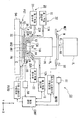
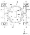
도 2 는 액체 공급 기구 및 액체 회수 기구를 나타내는 개략구성도이다.
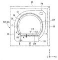
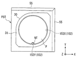
도 3 은 기판 스테이지의 평면도이다.
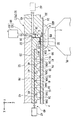
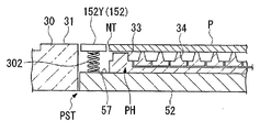
도 4 는 본 발명의 기판 스테이지의 일 실시형태를 나타내는 요부단면도이다.
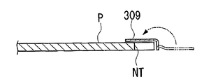
도 5 는 기판 스테이지에 대하여 착탈되는 기판 홀더를 나타내는 모식도이다.
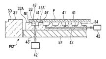
도 6 은 본 발명의 기판 스테이지의 다른 실시형태를 나타내는 요부단면도이다.
도 7a∼7c 는 공간에 액체를 배치하는 순서의 일례를 나타내는 모식도이다.
도 8 은 본 발명의 기판 스테이지의 다른 실시형태를 나타내는 요부단면도이다.
도 9 는 본 발명의 별도의 실시형태에 관련되는 기판 스테이지의 평면도이다.
도 10 은 본 발명의 별도의 실시형태에 관련되는 기판 스테이지의 평면도이다.
도 11 은 본 발명의 별도의 실시형태에 관련되는 기판 스테이지의 평면도이다.
도 12 는 본 발명의 별도의 실시형태에 관련되는 기판 스테이지의 평면도이다.
도 13 은 본 발명의 노광 방법에 관련되는 기판의 일 실시형태를 나타내는 도면이다.
도 14a∼14b 는 본 발명의 별도의 실시형태에 관련되는 기판 스테이지의 평면도이다.
도 15a∼15b 는, 본 발명의 별도의 실시형태에 관련되는 기판 스테이지의 평면도이다.
도 16a∼16b 는, 본 발명의 노광 방법에 관련되는 기판의 일 실시형태를 나타내는 도면이다.
도 17 은 본 발명의 노광 방법에 관련되는 기판의 일 실시형태를 나타내는 도면이다.
도 18 은 본 발명의 별도의 실시형태에 관련되는 기판 스테이지의 평면도이다.
도 19a∼19b 는 본 발명의 별도의 실시형태에 관련되는 기판 스테이지의 요부단면도이다.
도 20a∼20b 는 본 발명의 별도의 실시형태에 관련되는 기판 스테이지의 요부단면도이다.
도 21a∼21b 는 본 발명에 관련되는 갭 조정부의 별도의 실시형태를 나타내는 그림이다.
도 22 는, 본 발명에 관련되는 갭 조정부의 별도의 실시형태를 나타내는 도면이다.
도 23 은 본 발명에 관련되는 갭 조정부의 별도의 실시형태를 나타내는 도면이다.
도 24 는 본 발명의 별도의 실시형태에 관련되는 기판 스테이지의 요부단면도이다.
도 25a∼25b 는 본 발명의 별도의 실시형태에 관련되는 기판 스테이지의 도면이다.
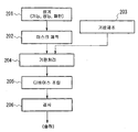
도 26 은 반도체 디바이스의 제조공정의 일례를 나타내는 플로우차트도이다.
도 27 은 종래의 노광 방법의 과제를 설명하기 위한 모식도이다.
Claims (1)
- 투영광학계와 액체를 통해 패턴의 이미지를 기판 상에 투영함으로써 상기 기판을 노광하는 노광 방법에 있어서,
상기 기판의 측면이 발액 처리되어 있는 것을 특징으로 하는 노광 방법.
Applications Claiming Priority (7)
| Application Number | Priority Date | Filing Date | Title |
|---|---|---|---|
| JPJP-P-2003-169904 | 2003-06-13 | ||
| JP2003169904 | 2003-06-13 | ||
| JP2003383887 | 2003-11-13 | ||
| JPJP-P-2003-383887 | 2003-11-13 | ||
| JPJP-P-2004-039654 | 2004-02-17 | ||
| JP2004039654 | 2004-02-17 | ||
| PCT/JP2004/008578 WO2004112108A1 (ja) | 2003-06-13 | 2004-06-11 | 露光方法、基板ステージ、露光装置、及びデバイス製造方法 |
Related Parent Applications (1)
| Application Number | Title | Priority Date | Filing Date |
|---|---|---|---|
| KR1020127025739A Division KR101528016B1 (ko) | 2003-06-13 | 2004-06-11 | 노광 방법, 기판 스테이지, 노광 장치, 및 디바이스 제조 방법 |
Publications (2)
| Publication Number | Publication Date |
|---|---|
| KR20130102645A true KR20130102645A (ko) | 2013-09-17 |
| KR101528089B1 KR101528089B1 (ko) | 2015-06-11 |
Family
ID=33556144
Family Applications (9)
| Application Number | Title | Priority Date | Filing Date |
|---|---|---|---|
| KR1020137020081A Expired - Fee Related KR101528089B1 (ko) | 2003-06-13 | 2004-06-11 | 노광 방법, 기판 스테이지, 노광 장치, 및 디바이스 제조 방법 |
| KR1020187028939A Ceased KR20180112884A (ko) | 2003-06-13 | 2004-06-11 | 노광 방법, 기판 스테이지, 노광 장치, 및 디바이스 제조 방법 |
| KR1020127028313A Expired - Fee Related KR101421866B1 (ko) | 2003-06-13 | 2004-06-11 | 노광 방법, 기판 스테이지, 노광 장치, 및 디바이스 제조 방법 |
| KR1020057023920A Expired - Fee Related KR101242815B1 (ko) | 2003-06-13 | 2004-06-11 | 노광 방법, 기판 스테이지, 노광 장치, 및 디바이스 제조방법 |
| KR1020157002702A Expired - Fee Related KR101729866B1 (ko) | 2003-06-13 | 2004-06-11 | 노광 방법, 기판 스테이지, 노광 장치, 및 디바이스 제조 방법 |
| KR1020147007168A Expired - Fee Related KR101520591B1 (ko) | 2003-06-13 | 2004-06-11 | 노광 방법, 기판 스테이지, 노광 장치, 및 디바이스 제조 방법 |
| KR1020117020347A Expired - Fee Related KR101290021B1 (ko) | 2003-06-13 | 2004-06-11 | 노광 방법, 기판 스테이지, 노광 장치, 및 디바이스 제조 방법 |
| KR1020127025739A Expired - Fee Related KR101528016B1 (ko) | 2003-06-13 | 2004-06-11 | 노광 방법, 기판 스테이지, 노광 장치, 및 디바이스 제조 방법 |
| KR1020167026062A Expired - Fee Related KR101940892B1 (ko) | 2003-06-13 | 2004-06-11 | 노광 방법, 기판 스테이지, 노광 장치, 및 디바이스 제조 방법 |
Family Applications After (8)
| Application Number | Title | Priority Date | Filing Date |
|---|---|---|---|
| KR1020187028939A Ceased KR20180112884A (ko) | 2003-06-13 | 2004-06-11 | 노광 방법, 기판 스테이지, 노광 장치, 및 디바이스 제조 방법 |
| KR1020127028313A Expired - Fee Related KR101421866B1 (ko) | 2003-06-13 | 2004-06-11 | 노광 방법, 기판 스테이지, 노광 장치, 및 디바이스 제조 방법 |
| KR1020057023920A Expired - Fee Related KR101242815B1 (ko) | 2003-06-13 | 2004-06-11 | 노광 방법, 기판 스테이지, 노광 장치, 및 디바이스 제조방법 |
| KR1020157002702A Expired - Fee Related KR101729866B1 (ko) | 2003-06-13 | 2004-06-11 | 노광 방법, 기판 스테이지, 노광 장치, 및 디바이스 제조 방법 |
| KR1020147007168A Expired - Fee Related KR101520591B1 (ko) | 2003-06-13 | 2004-06-11 | 노광 방법, 기판 스테이지, 노광 장치, 및 디바이스 제조 방법 |
| KR1020117020347A Expired - Fee Related KR101290021B1 (ko) | 2003-06-13 | 2004-06-11 | 노광 방법, 기판 스테이지, 노광 장치, 및 디바이스 제조 방법 |
| KR1020127025739A Expired - Fee Related KR101528016B1 (ko) | 2003-06-13 | 2004-06-11 | 노광 방법, 기판 스테이지, 노광 장치, 및 디바이스 제조 방법 |
| KR1020167026062A Expired - Fee Related KR101940892B1 (ko) | 2003-06-13 | 2004-06-11 | 노광 방법, 기판 스테이지, 노광 장치, 및 디바이스 제조 방법 |
Country Status (7)
| Country | Link |
|---|---|
| US (9) | US7483119B2 (ko) |
| EP (5) | EP3104396B1 (ko) |
| JP (11) | JP4415939B2 (ko) |
| KR (9) | KR101528089B1 (ko) |
| HK (1) | HK1258606A1 (ko) |
| TW (7) | TWI607292B (ko) |
| WO (1) | WO2004112108A1 (ko) |
Families Citing this family (141)
| Publication number | Priority date | Publication date | Assignee | Title |
|---|---|---|---|---|
| US9482966B2 (en) | 2002-11-12 | 2016-11-01 | Asml Netherlands B.V. | Lithographic apparatus and device manufacturing method |
| SG121819A1 (en) | 2002-11-12 | 2006-05-26 | Asml Netherlands Bv | Lithographic apparatus and device manufacturing method |
| US10503084B2 (en) | 2002-11-12 | 2019-12-10 | Asml Netherlands B.V. | Lithographic apparatus and device manufacturing method |
| EP3352010A1 (en) * | 2003-04-10 | 2018-07-25 | Nikon Corporation | Run-off path to collect liquid for an immersion lithography apparatus |
| US7213963B2 (en) | 2003-06-09 | 2007-05-08 | Asml Netherlands B.V. | Lithographic apparatus and device manufacturing method |
| EP3104396B1 (en) * | 2003-06-13 | 2018-03-21 | Nikon Corporation | Exposure method, substrate stage, exposure apparatus, and device manufacturing method |
| US6867844B2 (en) | 2003-06-19 | 2005-03-15 | Asml Holding N.V. | Immersion photolithography system and method using microchannel nozzles |
| DE60308161T2 (de) | 2003-06-27 | 2007-08-09 | Asml Netherlands B.V. | Lithographischer Apparat und Verfahren zur Herstellung eines Artikels |
| US6809794B1 (en) | 2003-06-27 | 2004-10-26 | Asml Holding N.V. | Immersion photolithography system and method using inverted wafer-projection optics interface |
| EP2264531B1 (en) | 2003-07-09 | 2013-01-16 | Nikon Corporation | Exposure apparatus and device manufacturing method |
| US7175968B2 (en) * | 2003-07-28 | 2007-02-13 | Asml Netherlands B.V. | Lithographic apparatus, device manufacturing method and a substrate |
| KR101613384B1 (ko) * | 2003-08-21 | 2016-04-18 | 가부시키가이샤 니콘 | 노광 장치, 노광 방법 및 디바이스 제조 방법 |
| KR101419192B1 (ko) | 2003-08-29 | 2014-07-15 | 가부시키가이샤 니콘 | 노광 장치 및 디바이스 제조 방법 |
| WO2005041276A1 (ja) * | 2003-10-28 | 2005-05-06 | Nikon Corporation | 露光装置、露光方法、デバイスの製造方法 |
| JP2005159322A (ja) * | 2003-10-31 | 2005-06-16 | Nikon Corp | 定盤、ステージ装置及び露光装置並びに露光方法 |
| US7528929B2 (en) * | 2003-11-14 | 2009-05-05 | Asml Netherlands B.V. | Lithographic apparatus and device manufacturing method |
| EP3370115A1 (en) | 2003-12-03 | 2018-09-05 | Nikon Corporation | Exposure apparatus, exposure method and method for producing a device |
| KR101281397B1 (ko) | 2003-12-15 | 2013-07-02 | 가부시키가이샤 니콘 | 스테이지 장치, 노광 장치, 및 노광 방법 |
| US7394521B2 (en) * | 2003-12-23 | 2008-07-01 | Asml Netherlands B.V. | Lithographic apparatus and device manufacturing method |
| KR101440743B1 (ko) * | 2004-01-05 | 2014-09-17 | 가부시키가이샤 니콘 | 노광 장치, 노광 방법 및 디바이스 제조 방법 |
| JP4572539B2 (ja) * | 2004-01-19 | 2010-11-04 | 株式会社ニコン | 露光装置及び露光方法、デバイス製造方法 |
| JP4973754B2 (ja) * | 2004-03-04 | 2012-07-11 | 株式会社ニコン | 露光方法及び露光装置、デバイス製造方法 |
| JP4622340B2 (ja) * | 2004-03-04 | 2011-02-02 | 株式会社ニコン | 露光装置、デバイス製造方法 |
| JP2005302880A (ja) * | 2004-04-08 | 2005-10-27 | Canon Inc | 液浸式露光装置 |
| US7898642B2 (en) | 2004-04-14 | 2011-03-01 | Asml Netherlands B.V. | Lithographic apparatus and device manufacturing method |
| CN103558737A (zh) * | 2004-06-09 | 2014-02-05 | 尼康股份有限公司 | 基板保持装置、具备其之曝光装置、方法 |
| JP4543767B2 (ja) * | 2004-06-10 | 2010-09-15 | 株式会社ニコン | 露光装置及びデバイス製造方法 |
| JP5119666B2 (ja) | 2004-06-21 | 2013-01-16 | 株式会社ニコン | 露光装置、液体除去方法、及びデバイス製造方法 |
| JP4677987B2 (ja) * | 2004-07-21 | 2011-04-27 | 株式会社ニコン | 露光方法及びデバイス製造方法 |
| US7701550B2 (en) | 2004-08-19 | 2010-04-20 | Asml Netherlands B.V. | Lithographic apparatus and device manufacturing method |
| US8102512B2 (en) | 2004-09-17 | 2012-01-24 | Nikon Corporation | Substrate holding device, exposure apparatus, and device manufacturing method |
| KR20070054635A (ko) * | 2004-09-17 | 2007-05-29 | 가부시키가이샤 니콘 | 노광용 기판, 노광 방법 및 디바이스 제조 방법 |
| EP1830394A4 (en) * | 2004-12-02 | 2009-05-27 | Nikon Corp | EXPOSURE APPARATUS, EXPOSURE METHOD, AND DEVICE MANUFACTURING METHOD |
| WO2006064851A1 (ja) | 2004-12-15 | 2006-06-22 | Nikon Corporation | 基板保持装置、露光装置、及びデバイス製造方法 |
| JP4551758B2 (ja) * | 2004-12-27 | 2010-09-29 | 株式会社東芝 | 液浸露光方法および半導体装置の製造方法 |
| JP4488890B2 (ja) | 2004-12-27 | 2010-06-23 | 株式会社東芝 | レジストパターン形成方法及び半導体装置の製造方法 |
| US7491661B2 (en) * | 2004-12-28 | 2009-02-17 | Asml Netherlands B.V. | Device manufacturing method, top coat material and substrate |
| DE602006012746D1 (de) | 2005-01-14 | 2010-04-22 | Asml Netherlands Bv | Lithografische Vorrichtung und Herstellungsverfahren |
| JP2006202825A (ja) * | 2005-01-18 | 2006-08-03 | Jsr Corp | 液浸型露光装置 |
| EP1843386A1 (en) * | 2005-01-18 | 2007-10-10 | Nikon Corporation | Liquid removing apparatus, exposure apparatus and device manufacturing method |
| JP5040646B2 (ja) * | 2005-03-23 | 2012-10-03 | 株式会社ニコン | 露光装置及び露光方法、並びにデバイス製造方法 |
| US20060232753A1 (en) | 2005-04-19 | 2006-10-19 | Asml Holding N.V. | Liquid immersion lithography system with tilted liquid flow |
| KR101396620B1 (ko) * | 2005-04-25 | 2014-05-16 | 가부시키가이샤 니콘 | 노광 방법, 노광 장치, 및 디바이스 제조 방법 |
| JP4752320B2 (ja) * | 2005-04-28 | 2011-08-17 | 株式会社ニコン | 基板保持装置及び露光装置、基板保持方法、露光方法、並びにデバイス製造方法 |
| US7433016B2 (en) * | 2005-05-03 | 2008-10-07 | Asml Netherlands B.V. | Lithographic apparatus and device manufacturing method |
| JP2006313766A (ja) * | 2005-05-06 | 2006-11-16 | Nikon Corp | 基板保持装置及びステージ装置並びに露光装置 |
| JP4761055B2 (ja) * | 2005-06-10 | 2011-08-31 | 信越化学工業株式会社 | パターン形成方法 |
| WO2007002833A2 (en) * | 2005-06-29 | 2007-01-04 | Blaise Corbett | Introduction of an intermediary refractive layer for immersion lithography |
| JP3997245B2 (ja) * | 2005-10-04 | 2007-10-24 | キヤノン株式会社 | 露光装置及びデバイス製造方法 |
| US7878791B2 (en) | 2005-11-04 | 2011-02-01 | Asml Netherlands B.V. | Imprint lithography |
| US8011915B2 (en) | 2005-11-04 | 2011-09-06 | Asml Netherlands B.V. | Imprint lithography |
| US7633073B2 (en) * | 2005-11-23 | 2009-12-15 | Asml Netherlands B.V. | Lithographic apparatus and device manufacturing method |
| US7773195B2 (en) | 2005-11-29 | 2010-08-10 | Asml Holding N.V. | System and method to increase surface tension and contact angle in immersion lithography |
| JP4968076B2 (ja) * | 2005-12-08 | 2012-07-04 | 株式会社ニコン | 基板保持装置、露光装置、露光方法、及びデバイス製造方法 |
| US7420194B2 (en) | 2005-12-27 | 2008-09-02 | Asml Netherlands B.V. | Lithographic apparatus and substrate edge seal |
| US7649611B2 (en) | 2005-12-30 | 2010-01-19 | Asml Netherlands B.V. | Lithographic apparatus and device manufacturing method |
| US7446859B2 (en) * | 2006-01-27 | 2008-11-04 | International Business Machines Corporation | Apparatus and method for reducing contamination in immersion lithography |
| US7310132B2 (en) * | 2006-03-17 | 2007-12-18 | Asml Netherlands B.V. | Lithographic apparatus and device manufacturing method |
| JP4889331B2 (ja) * | 2006-03-22 | 2012-03-07 | 大日本スクリーン製造株式会社 | 基板処理装置および基板処理方法 |
| CN100590173C (zh) * | 2006-03-24 | 2010-02-17 | 北京有色金属研究总院 | 一种荧光粉及其制造方法和所制成的电光源 |
| US8027019B2 (en) * | 2006-03-28 | 2011-09-27 | Asml Netherlands B.V. | Lithographic apparatus and device manufacturing method |
| EP2005222A4 (en) * | 2006-04-03 | 2010-07-28 | COMPARED TO IMMERSION LIQUIDS SOLVOPHOBE INSERTION SURFACES AND OPTICAL WINDOWS | |
| US7978308B2 (en) * | 2006-05-15 | 2011-07-12 | Asml Netherlands B.V. | Lithographic apparatus and device manufacturing method |
| CN102298274A (zh) * | 2006-05-18 | 2011-12-28 | 株式会社尼康 | 曝光方法及装置、维护方法、以及组件制造方法 |
| US20070273856A1 (en) | 2006-05-25 | 2007-11-29 | Nikon Corporation | Apparatus and methods for inhibiting immersion liquid from flowing below a substrate |
| JP2007335476A (ja) * | 2006-06-12 | 2007-12-27 | Canon Inc | 露光装置及びデバイス製造方法 |
| US20080043211A1 (en) * | 2006-08-21 | 2008-02-21 | Nikon Corporation | Apparatus and methods for recovering fluid in immersion lithography |
| US7826030B2 (en) * | 2006-09-07 | 2010-11-02 | Asml Netherlands B.V. | Lithographic apparatus and device manufacturing method |
| JP2008108766A (ja) * | 2006-10-23 | 2008-05-08 | Toppan Printing Co Ltd | チャックおよびスピンコータ装置 |
| US20080100812A1 (en) * | 2006-10-26 | 2008-05-01 | Nikon Corporation | Immersion lithography system and method having a wafer chuck made of a porous material |
| US8253922B2 (en) | 2006-11-03 | 2012-08-28 | Taiwan Semiconductor Manufacturing Company, Ltd. | Immersion lithography system using a sealed wafer bath |
| US8208116B2 (en) * | 2006-11-03 | 2012-06-26 | Taiwan Semiconductor Manufacturing Company, Ltd. | Immersion lithography system using a sealed wafer bath |
| US20080137055A1 (en) * | 2006-12-08 | 2008-06-12 | Asml Netherlands B.V. | Lithographic apparatus and device manufacturing method |
| US8416383B2 (en) * | 2006-12-13 | 2013-04-09 | Asml Netherlands B.V. | Lithographic apparatus and method |
| US20080241489A1 (en) * | 2007-03-30 | 2008-10-02 | Renesas Technology Corp. | Method of forming resist pattern and semiconductor device manufactured with the same |
| US8514365B2 (en) * | 2007-06-01 | 2013-08-20 | Asml Netherlands B.V. | Lithographic apparatus and device manufacturing method |
| US20080304025A1 (en) * | 2007-06-08 | 2008-12-11 | Taiwan Semiconductor Manufacturing Company, Ltd. | Apparatus and method for immersion lithography |
| US7561250B2 (en) * | 2007-06-19 | 2009-07-14 | Asml Netherlands B.V. | Lithographic apparatus having parts with a coated film adhered thereto |
| TWI450047B (zh) * | 2007-07-13 | 2014-08-21 | 瑪波微影Ip公司 | 微影系統、夾緊方法及晶圓台 |
| US8705010B2 (en) * | 2007-07-13 | 2014-04-22 | Mapper Lithography Ip B.V. | Lithography system, method of clamping and wafer table |
| JP4961299B2 (ja) * | 2007-08-08 | 2012-06-27 | キヤノン株式会社 | 露光装置およびデバイス製造方法 |
| JP4533416B2 (ja) * | 2007-09-25 | 2010-09-01 | キヤノン株式会社 | 露光装置およびデバイス製造方法 |
| JP5369443B2 (ja) * | 2008-02-05 | 2013-12-18 | 株式会社ニコン | ステージ装置、露光装置、露光方法、及びデバイス製造方法 |
| US20090218743A1 (en) * | 2008-02-29 | 2009-09-03 | Nikon Corporation | Substrate holding apparatus, exposure apparatus, exposing method, device fabricating method, plate member, and wall |
| JP2009260264A (ja) * | 2008-03-24 | 2009-11-05 | Canon Inc | 露光装置およびデバイス製造方法 |
| US9176393B2 (en) * | 2008-05-28 | 2015-11-03 | Asml Netherlands B.V. | Lithographic apparatus and a method of operating the apparatus |
| NL1036924A1 (nl) * | 2008-06-02 | 2009-12-03 | Asml Netherlands Bv | Substrate table, lithographic apparatus and device manufacturing method. |
| NL2002983A1 (nl) * | 2008-06-26 | 2009-12-29 | Asml Netherlands Bv | A lithographic apparatus and a method of operating the lithographic apparatus. |
| JP2010021370A (ja) * | 2008-07-10 | 2010-01-28 | Canon Inc | 液浸露光装置およびデバイス製造方法 |
| JP2010140958A (ja) * | 2008-12-09 | 2010-06-24 | Canon Inc | 露光装置及びデバイス製造方法 |
| EP2196857A3 (en) | 2008-12-09 | 2010-07-21 | ASML Netherlands BV | Lithographic apparatus and device manufacturing method |
| JP5001343B2 (ja) | 2008-12-11 | 2012-08-15 | エーエスエムエル ネザーランズ ビー.ブイ. | 流体抽出システム、液浸リソグラフィ装置、及び液浸リソグラフィ装置で使用される液浸液の圧力変動を低減する方法 |
| JP4853530B2 (ja) * | 2009-02-27 | 2012-01-11 | 株式会社豊田中央研究所 | 可動部を有するマイクロデバイス |
| JP5398307B2 (ja) * | 2009-03-06 | 2014-01-29 | 株式会社東芝 | 半導体装置の製造方法 |
| NL2004305A (en) | 2009-03-13 | 2010-09-14 | Asml Netherlands Bv | Substrate table, immersion lithographic apparatus and device manufacturing method. |
| NL2004807A (en) * | 2009-06-30 | 2011-01-04 | Asml Netherlands Bv | Substrate table for a lithographic apparatus, litographic apparatus, method of using a substrate table and device manufacturing method. |
| US8913230B2 (en) * | 2009-07-02 | 2014-12-16 | Canon Nanotechnologies, Inc. | Chucking system with recessed support feature |
| NL2005120A (en) * | 2009-09-21 | 2011-03-22 | Asml Netherlands Bv | Lithographic apparatus, coverplate and device manufacturing method. |
| NL2005126A (en) * | 2009-09-21 | 2011-03-22 | Asml Netherlands Bv | Lithographic apparatus, coverplate and device manufacturing method. |
| NL2005666A (en) * | 2009-12-18 | 2011-06-21 | Asml Netherlands Bv | A lithographic apparatus and a device manufacturing method. |
| NL2005874A (en) * | 2010-01-22 | 2011-07-25 | Asml Netherlands Bv | A lithographic apparatus and a device manufacturing method. |
| TW201630105A (zh) * | 2015-02-12 | 2016-08-16 | 漢民科技股份有限公司 | 晶圓保持器 |
| US8298729B2 (en) | 2010-03-18 | 2012-10-30 | Micron Technology, Inc. | Microlithography masks including image reversal assist features, microlithography systems including such masks, and methods of forming such masks |
| JP5131312B2 (ja) * | 2010-04-26 | 2013-01-30 | 株式会社ニコン | 露光装置、露光方法、及びデバイス製造方法 |
| US8598538B2 (en) * | 2010-09-07 | 2013-12-03 | Nikon Corporation | Movable body apparatus, object processing device, exposure apparatus, flat-panel display manufacturing method, and device manufacturing method |
| NL2007802A (en) | 2010-12-21 | 2012-06-25 | Asml Netherlands Bv | A substrate table, a lithographic apparatus and a device manufacturing method. |
| US9329496B2 (en) * | 2011-07-21 | 2016-05-03 | Nikon Corporation | Exposure apparatus, exposure method, method of manufacturing device, program, and storage medium |
| EP2749534B1 (en) | 2011-10-18 | 2018-12-19 | Toagosei Co., Ltd. | Method for producing chloropolysilane, and fluid bed reaction device |
| EP3683627A1 (en) | 2012-02-03 | 2020-07-22 | ASML Netherlands B.V. | Substrate holder and lithographic apparatus |
| EP2856262B1 (en) | 2012-05-29 | 2019-09-25 | ASML Netherlands B.V. | Support apparatus, lithographic apparatus and device manufacturing method |
| JP2014045090A (ja) * | 2012-08-27 | 2014-03-13 | Toshiba Corp | 液浸露光装置 |
| JP6155581B2 (ja) * | 2012-09-14 | 2017-07-05 | 株式会社ニコン | 露光装置、露光方法、デバイス製造方法 |
| JP6262866B2 (ja) * | 2014-01-20 | 2018-01-17 | エーエスエムエル ネザーランズ ビー.ブイ. | リソグラフィのための支持テーブル、リソグラフィ装置、及びデバイス製造方法 |
| CN107004574B (zh) * | 2014-12-12 | 2020-06-30 | 佳能株式会社 | 基板保持装置、光刻设备以及物品制造方法 |
| KR102558072B1 (ko) * | 2015-03-31 | 2023-07-20 | 가부시키가이샤 니콘 | 노광 장치, 플랫 패널 디스플레이의 제조 방법, 디바이스 제조 방법, 및 노광 방법 |
| WO2016198255A1 (en) * | 2015-06-11 | 2016-12-15 | Asml Netherlands B.V. | Lithographic apparatus and method for loading a substrate |
| WO2016207122A1 (en) | 2015-06-23 | 2016-12-29 | Asml Netherlands B.V. | Support apparatus, lithographic apparatus and device manufacturing method |
| US10254256B2 (en) | 2015-10-01 | 2019-04-09 | Thermo Hypersil-Keystone Llc | Method of packing chromatographic columns, packed chromatographic columns for use at high pressures and uses thereof |
| JP6751759B2 (ja) | 2015-12-08 | 2020-09-09 | エーエスエムエル ネザーランズ ビー.ブイ. | 基板テーブル、リソグラフィ装置、及びリソグラフィ装置を操作する方法 |
| JP6648266B2 (ja) | 2015-12-15 | 2020-02-14 | エーエスエムエル ネザーランズ ビー.ブイ. | 基板ホルダ、リソグラフィ装置、及びデバイスを製造する方法 |
| NL2018653A (en) * | 2016-05-12 | 2017-11-15 | Asml Netherlands Bv | Extraction body for lithographic apparatus |
| US10185226B2 (en) * | 2016-07-14 | 2019-01-22 | Canon Kabushiki Kaisha | Stage apparatus, lithography apparatus, and method of manufacturing article |
| KR20180064605A (ko) * | 2016-12-05 | 2018-06-15 | 삼성디스플레이 주식회사 | 레이저 가공용 워크 테이블 및 이의 동작 방법 |
| JP6978840B2 (ja) * | 2017-02-28 | 2021-12-08 | 株式会社Screenホールディングス | 基板処理装置および基板保持装置 |
| KR102450292B1 (ko) * | 2017-06-06 | 2022-10-04 | 에이에스엠엘 네델란즈 비.브이. | 지지 테이블로부터 대상물을 언로딩하는 방법 |
| JP6418281B2 (ja) * | 2017-06-07 | 2018-11-07 | 株式会社ニコン | 露光装置 |
| WO2018233825A1 (en) * | 2017-06-21 | 2018-12-27 | Hp Indigo B.V. | VACUUM TABLES |
| KR102709422B1 (ko) | 2017-10-12 | 2024-09-25 | 에이에스엠엘 네델란즈 비.브이. | 리소그래피 장치에 사용하기 위한 기판 홀더 |
| EP3707747A4 (en) | 2017-11-10 | 2021-07-28 | Applied Materials, Inc. | PATTERNED CHUCK FOR DOUBLE-SIDED MACHINING |
| JP7164605B2 (ja) | 2017-12-13 | 2022-11-01 | エーエスエムエル ネザーランズ ビー.ブイ. | リソグラフィ装置で使用するための基板ホルダ |
| JP2019193995A (ja) * | 2018-05-02 | 2019-11-07 | カンタツ株式会社 | 積層造形装置および積層造形装置の制御方法 |
| WO2019226525A1 (en) * | 2018-05-23 | 2019-11-28 | Ii-Vi Delaware, Inc. | Apparatus for supporting thinned semiconductor wafers |
| GB2575623B (en) | 2018-06-04 | 2022-10-26 | Tdeltas Ltd | 3-hydroxybutyrate esters for treating cancer cachexia |
| JP2019032552A (ja) * | 2018-10-10 | 2019-02-28 | 株式会社ニコン | 露光装置、露光方法、デバイス製造方法 |
| US11482417B2 (en) * | 2019-08-23 | 2022-10-25 | Taiwan Semiconductor Manufacturing Company Ltd. | Method of manufacturing semiconductor structure |
| US11638882B2 (en) * | 2020-04-26 | 2023-05-02 | Shantou Chenghai Lichengfeng Plastic Products Factory | Wall-climbing vehicle and bottom cover of such vehicle |
| KR102381348B1 (ko) * | 2020-10-29 | 2022-03-30 | 한국전기연구원 | 탄화규소 웨이퍼의 tsd와 ted 결함 비파괴 분석법 |
| JP7532234B2 (ja) * | 2020-12-10 | 2024-08-13 | キヤノン株式会社 | 平坦化装置、平坦化方法及び物品の製造方法 |
| KR20220090909A (ko) | 2020-12-23 | 2022-06-30 | 정주은 | 수분 감지센서를 이용한 화분 관리 |
| CN113411937B (zh) * | 2021-05-07 | 2022-12-27 | 深圳市声光行科技发展有限公司 | 一种舞台灯光控制平台 |
| EP4540659A1 (en) * | 2022-06-15 | 2025-04-23 | ASML Netherlands B.V. | Substrate support and lithographic apparatus |
Family Cites Families (258)
| Publication number | Priority date | Publication date | Assignee | Title |
|---|---|---|---|---|
| US221563A (en) * | 1879-11-11 | Arthur l | ||
| DE221563C (ko) | ||||
| US4346164A (en) * | 1980-10-06 | 1982-08-24 | Werner Tabarelli | Photolithographic method for the manufacture of integrated circuits |
| JPS57117238A (en) | 1981-01-14 | 1982-07-21 | Nippon Kogaku Kk <Nikon> | Exposing and baking device for manufacturing integrated circuit with illuminometer |
| JPS57153433A (en) * | 1981-03-18 | 1982-09-22 | Hitachi Ltd | Manufacturing device for semiconductor |
| JPS58202448A (ja) | 1982-05-21 | 1983-11-25 | Hitachi Ltd | 露光装置 |
| JPS5919912A (ja) | 1982-07-26 | 1984-02-01 | Hitachi Ltd | 液浸距離保持装置 |
| DD221563A1 (de) * | 1983-09-14 | 1985-04-24 | Mikroelektronik Zt Forsch Tech | Immersionsobjektiv fuer die schrittweise projektionsabbildung einer maskenstruktur |
| DD224448A1 (de) | 1984-03-01 | 1985-07-03 | Zeiss Jena Veb Carl | Einrichtung zur fotolithografischen strukturuebertragung |
| JPS6265326A (ja) | 1985-09-18 | 1987-03-24 | Hitachi Ltd | 露光装置 |
| JPS62221130A (ja) * | 1986-03-24 | 1987-09-29 | Toshiba Corp | 真空チヤツク装置 |
| JPS6394627A (ja) * | 1986-10-09 | 1988-04-25 | Nec Corp | 半導体の製造装置 |
| JPS63157419A (ja) | 1986-12-22 | 1988-06-30 | Toshiba Corp | 微細パタ−ン転写装置 |
| JPH0793254B2 (ja) * | 1987-07-22 | 1995-10-09 | 松下電子工業株式会社 | レジスト膜形成用基板の処理方法 |
| JPH0831515B2 (ja) * | 1988-06-21 | 1996-03-27 | 株式会社ニコン | 基板の吸着装置 |
| JP2978192B2 (ja) | 1990-02-19 | 1999-11-15 | 株式会社ピュアレックス | 半導体ウエハー試料作成法 |
| JP2897355B2 (ja) | 1990-07-05 | 1999-05-31 | 株式会社ニコン | アライメント方法,露光装置,並びに位置検出方法及び装置 |
| JPH04305915A (ja) | 1991-04-02 | 1992-10-28 | Nikon Corp | 密着型露光装置 |
| JPH04305917A (ja) | 1991-04-02 | 1992-10-28 | Nikon Corp | 密着型露光装置 |
| JPH0562877A (ja) | 1991-09-02 | 1993-03-12 | Yasuko Shinohara | 光によるlsi製造縮小投影露光装置の光学系 |
| JPH05235151A (ja) * | 1992-02-20 | 1993-09-10 | Canon Inc | 基板保持盤 |
| JP3246615B2 (ja) | 1992-07-27 | 2002-01-15 | 株式会社ニコン | 照明光学装置、露光装置、及び露光方法 |
| JPH06188169A (ja) | 1992-08-24 | 1994-07-08 | Canon Inc | 結像方法及び該方法を用いる露光装置及び該方法を用いるデバイス製造方法 |
| JPH06124873A (ja) * | 1992-10-09 | 1994-05-06 | Canon Inc | 液浸式投影露光装置 |
| JP2753930B2 (ja) | 1992-11-27 | 1998-05-20 | キヤノン株式会社 | 液浸式投影露光装置 |
| US5591958A (en) | 1993-06-14 | 1997-01-07 | Nikon Corporation | Scanning exposure method and apparatus |
| JP3412704B2 (ja) | 1993-02-26 | 2003-06-03 | 株式会社ニコン | 投影露光方法及び装置、並びに露光装置 |
| JPH06326174A (ja) * | 1993-05-12 | 1994-11-25 | Hitachi Ltd | ウェハ真空吸着装置 |
| JPH0781978A (ja) | 1993-06-18 | 1995-03-28 | Olympus Optical Co Ltd | ガラス製光学部品における撥水性を有する反射防止膜 |
| JP2890089B2 (ja) * | 1993-09-06 | 1999-05-10 | 東京エレクトロン株式会社 | 処理装置 |
| JPH07220990A (ja) * | 1994-01-28 | 1995-08-18 | Hitachi Ltd | パターン形成方法及びその露光装置 |
| US5874820A (en) | 1995-04-04 | 1999-02-23 | Nikon Corporation | Window frame-guided stage mechanism |
| US5528118A (en) | 1994-04-01 | 1996-06-18 | Nikon Precision, Inc. | Guideless stage with isolated reaction stage |
| JP3555230B2 (ja) | 1994-05-18 | 2004-08-18 | 株式会社ニコン | 投影露光装置 |
| US5623853A (en) | 1994-10-19 | 1997-04-29 | Nikon Precision Inc. | Precision motion stage with single guide beam and follower stage |
| JP3387075B2 (ja) | 1994-12-12 | 2003-03-17 | 株式会社ニコン | 走査露光方法、露光装置、及び走査型露光装置 |
| JPH08250402A (ja) | 1995-03-15 | 1996-09-27 | Nikon Corp | 走査型露光方法及び装置 |
| JP3312164B2 (ja) * | 1995-04-07 | 2002-08-05 | 日本電信電話株式会社 | 真空吸着装置 |
| JPH0936212A (ja) * | 1995-05-16 | 1997-02-07 | Shinko Electric Co Ltd | 静電チャック |
| JPH08316125A (ja) | 1995-05-19 | 1996-11-29 | Hitachi Ltd | 投影露光方法及び露光装置 |
| JPH08316124A (ja) | 1995-05-19 | 1996-11-29 | Hitachi Ltd | 投影露光方法及び露光装置 |
| US5923408A (en) * | 1996-01-31 | 1999-07-13 | Canon Kabushiki Kaisha | Substrate holding system and exposure apparatus using the same |
| JPH1049504A (ja) * | 1996-08-02 | 1998-02-20 | Mitsubishi Electric Corp | 負荷分散バッチシステム |
| US5825043A (en) * | 1996-10-07 | 1998-10-20 | Nikon Precision Inc. | Focusing and tilting adjustment system for lithography aligner, manufacturing apparatus or inspection apparatus |
| JP4029182B2 (ja) | 1996-11-28 | 2008-01-09 | 株式会社ニコン | 露光方法 |
| JP4029183B2 (ja) | 1996-11-28 | 2008-01-09 | 株式会社ニコン | 投影露光装置及び投影露光方法 |
| EP1944654A3 (en) | 1996-11-28 | 2010-06-02 | Nikon Corporation | An exposure apparatus and an exposure method |
| WO1998028665A1 (en) | 1996-12-24 | 1998-07-02 | Koninklijke Philips Electronics N.V. | Two-dimensionally balanced positioning device with two object holders, and lithographic device provided with such a positioning device |
| JPH10255319A (ja) * | 1997-03-12 | 1998-09-25 | Hitachi Maxell Ltd | 原盤露光装置及び方法 |
| JP3747566B2 (ja) * | 1997-04-23 | 2006-02-22 | 株式会社ニコン | 液浸型露光装置 |
| JP3817836B2 (ja) * | 1997-06-10 | 2006-09-06 | 株式会社ニコン | 露光装置及びその製造方法並びに露光方法及びデバイス製造方法 |
| US6381013B1 (en) | 1997-06-25 | 2002-04-30 | Northern Edge Associates | Test slide for microscopes and method for the production of such a slide |
| JPH1116816A (ja) | 1997-06-25 | 1999-01-22 | Nikon Corp | 投影露光装置、該装置を用いた露光方法、及び該装置を用いた回路デバイスの製造方法 |
| JP4001661B2 (ja) * | 1997-07-08 | 2007-10-31 | 沖電気工業株式会社 | ウェハ載置台、ウェハ裏面の処理方法、露光装置、および回転塗布装置 |
| JPH11111819A (ja) * | 1997-09-30 | 1999-04-23 | Asahi Kasei Micro Syst Co Ltd | ウェハーの固定方法及び露光装置 |
| JP4210871B2 (ja) | 1997-10-31 | 2009-01-21 | 株式会社ニコン | 露光装置 |
| JPH11163103A (ja) * | 1997-11-25 | 1999-06-18 | Hitachi Ltd | 半導体装置の製造方法および製造装置 |
| JPH11176727A (ja) * | 1997-12-11 | 1999-07-02 | Nikon Corp | 投影露光装置 |
| US6208407B1 (en) | 1997-12-22 | 2001-03-27 | Asm Lithography B.V. | Method and apparatus for repetitively projecting a mask pattern on a substrate, using a time-saving height measurement |
| KR100638533B1 (ko) * | 1998-02-09 | 2006-10-26 | 가부시키가이샤 니콘 | 기판지지장치, 기판반송장치 및 그 방법, 기판교환방법,그리고 노광장치 및 그 제조방법 |
| JPH11239758A (ja) * | 1998-02-26 | 1999-09-07 | Dainippon Screen Mfg Co Ltd | 基板処理装置 |
| WO1999049504A1 (fr) * | 1998-03-26 | 1999-09-30 | Nikon Corporation | Procede et systeme d'exposition par projection |
| EP1079223A4 (en) | 1998-05-19 | 2002-11-27 | Nikon Corp | INSTRUMENT AND METHOD FOR MEASURING ABERATIONS, PROJECTION DEVICE INCLUDING THIS INSTRUMENT AND ITS MANUFACTURING METHOD |
| US6819414B1 (en) | 1998-05-19 | 2004-11-16 | Nikon Corporation | Aberration measuring apparatus, aberration measuring method, projection exposure apparatus having the same measuring apparatus, device manufacturing method using the same measuring method, and exposure method |
| US6036586A (en) | 1998-07-29 | 2000-03-14 | Micron Technology, Inc. | Apparatus and method for reducing removal forces for CMP pads |
| JP2000058436A (ja) * | 1998-08-11 | 2000-02-25 | Nikon Corp | 投影露光装置及び露光方法 |
| AU4779600A (en) | 1999-05-20 | 2000-12-12 | Nikon Corporation | Container for holder exposure apparatus, device manufacturing method, and device manufacturing apparatus |
| AU5653699A (en) | 1999-09-20 | 2001-04-24 | Nikon Corporation | Parallel link mechanism, exposure system and method of manufacturing the same, and method of manufacturing devices |
| US7187503B2 (en) | 1999-12-29 | 2007-03-06 | Carl Zeiss Smt Ag | Refractive projection objective for immersion lithography |
| US6995930B2 (en) | 1999-12-29 | 2006-02-07 | Carl Zeiss Smt Ag | Catadioptric projection objective with geometric beam splitting |
| KR100804006B1 (ko) * | 2000-01-28 | 2008-02-18 | 히다치 도쿄 에렉트로닉스 가부시키가이샤 | 웨이퍼 척 |
| JP2001332609A (ja) * | 2000-03-13 | 2001-11-30 | Nikon Corp | 基板保持装置及び露光装置 |
| US6614504B2 (en) | 2000-03-30 | 2003-09-02 | Nikon Corporation | Exposure apparatus, exposure method, and device manufacturing method |
| US20020041377A1 (en) | 2000-04-25 | 2002-04-11 | Nikon Corporation | Aerial image measurement method and unit, optical properties measurement method and unit, adjustment method of projection optical system, exposure method and apparatus, making method of exposure apparatus, and device manufacturing method |
| JP2002014005A (ja) | 2000-04-25 | 2002-01-18 | Nikon Corp | 空間像計測方法、結像特性計測方法、空間像計測装置及び露光装置 |
| KR100866818B1 (ko) | 2000-12-11 | 2008-11-04 | 가부시키가이샤 니콘 | 투영광학계 및 이 투영광학계를 구비한 노광장치 |
| JP2002229215A (ja) * | 2001-01-30 | 2002-08-14 | Nikon Corp | 露光方法及び露光装置 |
| EP1231514A1 (en) | 2001-02-13 | 2002-08-14 | Asm Lithography B.V. | Measurement of wavefront aberrations in a lithographic projection apparatus |
| JP2002248344A (ja) * | 2001-02-26 | 2002-09-03 | Nikon Corp | 極端紫外光発生装置並びにそれを用いた露光装置及び半導体製造方法 |
| WO2002091078A1 (en) | 2001-05-07 | 2002-11-14 | Massachusetts Institute Of Technology | Methods and apparatus employing an index matching medium |
| JP4412450B2 (ja) | 2001-10-05 | 2010-02-10 | 信越化学工業株式会社 | 反射防止フィルター |
| EP1300433B1 (en) | 2001-10-05 | 2008-10-15 | Shin-Etsu Chemical Co., Ltd. | Perfluoropolyether-modified silane, surface treating agent, and antireflection filter |
| JP2003124089A (ja) * | 2001-10-09 | 2003-04-25 | Nikon Corp | 荷電粒子線露光装置及び露光方法 |
| TW521320B (en) | 2001-12-10 | 2003-02-21 | Via Tech Inc | Device and method for substrate exposure |
| JP2003240906A (ja) | 2002-02-20 | 2003-08-27 | Dainippon Printing Co Ltd | 反射防止体およびその製造方法 |
| DE10229818A1 (de) | 2002-06-28 | 2004-01-15 | Carl Zeiss Smt Ag | Verfahren zur Fokusdetektion und Abbildungssystem mit Fokusdetektionssystem |
| US7092069B2 (en) | 2002-03-08 | 2006-08-15 | Carl Zeiss Smt Ag | Projection exposure method and projection exposure system |
| DE10210899A1 (de) | 2002-03-08 | 2003-09-18 | Zeiss Carl Smt Ag | Refraktives Projektionsobjektiv für Immersions-Lithographie |
| US6828542B2 (en) | 2002-06-07 | 2004-12-07 | Brion Technologies, Inc. | System and method for lithography process monitoring and control |
| US6882406B2 (en) | 2002-06-14 | 2005-04-19 | Asml Netherlands B.V. | Euv lithographic projection apparatus comprising an optical element with a self-assembled monolayer, optical element with a self-assembled monolayer, method of applying a self-assembled monolayer, device manufacturing method and device manufactured thereby |
| KR20050035890A (ko) | 2002-08-23 | 2005-04-19 | 가부시키가이샤 니콘 | 투영 광학계, 포토리소그래피 방법, 노광 장치 및 그 이용방법 |
| US6954993B1 (en) | 2002-09-30 | 2005-10-18 | Lam Research Corporation | Concentric proximity processing head |
| US7367345B1 (en) | 2002-09-30 | 2008-05-06 | Lam Research Corporation | Apparatus and method for providing a confined liquid for immersion lithography |
| US7093375B2 (en) | 2002-09-30 | 2006-08-22 | Lam Research Corporation | Apparatus and method for utilizing a meniscus in substrate processing |
| US6988327B2 (en) | 2002-09-30 | 2006-01-24 | Lam Research Corporation | Methods and systems for processing a substrate using a dynamic liquid meniscus |
| US7383843B2 (en) | 2002-09-30 | 2008-06-10 | Lam Research Corporation | Method and apparatus for processing wafer surfaces using thin, high velocity fluid layer |
| US6988326B2 (en) | 2002-09-30 | 2006-01-24 | Lam Research Corporation | Phobic barrier meniscus separation and containment |
| US6788477B2 (en) | 2002-10-22 | 2004-09-07 | Taiwan Semiconductor Manufacturing Co., Ltd. | Apparatus for method for immersion lithography |
| DE60335595D1 (de) | 2002-11-12 | 2011-02-17 | Asml Netherlands Bv | Lithographischer Apparat mit Immersion und Verfahren zur Herstellung einer Vorrichtung |
| SG121822A1 (en) | 2002-11-12 | 2006-05-26 | Asml Netherlands Bv | Lithographic apparatus and device manufacturing method |
| US7110081B2 (en) | 2002-11-12 | 2006-09-19 | Asml Netherlands B.V. | Lithographic apparatus and device manufacturing method |
| SG135052A1 (en) | 2002-11-12 | 2007-09-28 | Asml Netherlands Bv | Lithographic apparatus and device manufacturing method |
| EP1429188B1 (en) * | 2002-11-12 | 2013-06-19 | ASML Netherlands B.V. | Lithographic projection apparatus |
| CN101470360B (zh) | 2002-11-12 | 2013-07-24 | Asml荷兰有限公司 | 光刻装置和器件制造方法 |
| SG121819A1 (en) * | 2002-11-12 | 2006-05-26 | Asml Netherlands Bv | Lithographic apparatus and device manufacturing method |
| SG131766A1 (en) | 2002-11-18 | 2007-05-28 | Asml Netherlands Bv | Lithographic apparatus and device manufacturing method |
| DE10253679A1 (de) | 2002-11-18 | 2004-06-03 | Infineon Technologies Ag | Optische Einrichtung zur Verwendung bei einem Lithographie-Verfahren, insbesondere zur Herstellung eines Halbleiter-Bauelements, sowie optisches Lithographieverfahren |
| DE10258718A1 (de) | 2002-12-09 | 2004-06-24 | Carl Zeiss Smt Ag | Projektionsobjektiv, insbesondere für die Mikrolithographie, sowie Verfahren zur Abstimmung eines Projektionsobjektives |
| JP4595320B2 (ja) | 2002-12-10 | 2010-12-08 | 株式会社ニコン | 露光装置、及びデバイス製造方法 |
| SG157962A1 (en) * | 2002-12-10 | 2010-01-29 | Nikon Corp | Exposure apparatus and method for producing device |
| US6992750B2 (en) | 2002-12-10 | 2006-01-31 | Canon Kabushiki Kaisha | Exposure apparatus and method |
| KR101101737B1 (ko) | 2002-12-10 | 2012-01-05 | 가부시키가이샤 니콘 | 노광장치 및 노광방법, 디바이스 제조방법 |
| EP1571697A4 (en) | 2002-12-10 | 2007-07-04 | Nikon Corp | EXPOSURE SYSTEM AND COMPONENT MANUFACTURING METHOD |
| CN100370533C (zh) | 2002-12-13 | 2008-02-20 | 皇家飞利浦电子股份有限公司 | 用于照射层的方法和用于将辐射导向层的装置 |
| US7010958B2 (en) | 2002-12-19 | 2006-03-14 | Asml Holding N.V. | High-resolution gas gauge proximity sensor |
| ATE365962T1 (de) | 2002-12-19 | 2007-07-15 | Koninkl Philips Electronics Nv | Verfahren und anordnung zum bestrahlen einer schicht mittels eines lichtpunkts |
| EP1584089B1 (en) | 2002-12-19 | 2006-08-02 | Koninklijke Philips Electronics N.V. | Method and device for irradiating spots on a layer |
| US6781670B2 (en) | 2002-12-30 | 2004-08-24 | Intel Corporation | Immersion lithography |
| JP2005250511A (ja) * | 2003-02-20 | 2005-09-15 | Tokyo Ohka Kogyo Co Ltd | 液浸露光プロセス用レジスト保護膜形成用材料、該保護膜形成材料による保護膜を有するレジスト膜、および該保護膜を用いたレジストパターン形成方法 |
| TW200424767A (en) * | 2003-02-20 | 2004-11-16 | Tokyo Ohka Kogyo Co Ltd | Immersion exposure process-use resist protection film forming material, composite film, and resist pattern forming method |
| US7090964B2 (en) | 2003-02-21 | 2006-08-15 | Asml Holding N.V. | Lithographic printing with polarized light |
| US6943941B2 (en) | 2003-02-27 | 2005-09-13 | Asml Netherlands B.V. | Stationary and dynamic radial transverse electric polarizer for high numerical aperture systems |
| US7206059B2 (en) | 2003-02-27 | 2007-04-17 | Asml Netherlands B.V. | Stationary and dynamic radial transverse electric polarizer for high numerical aperture systems |
| US7029832B2 (en) | 2003-03-11 | 2006-04-18 | Samsung Electronics Co., Ltd. | Immersion lithography methods using carbon dioxide |
| US20050164522A1 (en) | 2003-03-24 | 2005-07-28 | Kunz Roderick R. | Optical fluids, and systems and methods of making and using the same |
| KR20110104084A (ko) | 2003-04-09 | 2011-09-21 | 가부시키가이샤 니콘 | 액침 리소그래피 유체 제어 시스템 |
| EP3352010A1 (en) | 2003-04-10 | 2018-07-25 | Nikon Corporation | Run-off path to collect liquid for an immersion lithography apparatus |
| KR101431938B1 (ko) | 2003-04-10 | 2014-08-19 | 가부시키가이샤 니콘 | 액침 리소그래피 장치용 운반 영역을 포함하는 환경 시스템 |
| SG141426A1 (en) | 2003-04-10 | 2008-04-28 | Nikon Corp | Environmental system including vacuum scavange for an immersion lithography apparatus |
| JP4656057B2 (ja) | 2003-04-10 | 2011-03-23 | 株式会社ニコン | 液浸リソグラフィ装置用電気浸透素子 |
| JP4582089B2 (ja) | 2003-04-11 | 2010-11-17 | 株式会社ニコン | 液浸リソグラフィ用の液体噴射回収システム |
| KR101289959B1 (ko) | 2003-04-11 | 2013-07-26 | 가부시키가이샤 니콘 | 액침 리소그래피에 의한 광학기기의 세정방법 |
| SG139733A1 (en) | 2003-04-11 | 2008-02-29 | Nikon Corp | Apparatus having an immersion fluid system configured to maintain immersion fluid in a gap adjacent an optical assembly |
| KR20050122269A (ko) | 2003-04-17 | 2005-12-28 | 가부시키가이샤 니콘 | 액침 리소그래피를 이용하기 위한 오토포커스 소자의광학적 배열 |
| TW200424730A (en) | 2003-05-03 | 2004-11-16 | Jiahn-Chang Wu | Projector with UV light source. |
| JP4146755B2 (ja) | 2003-05-09 | 2008-09-10 | 松下電器産業株式会社 | パターン形成方法 |
| JP4025683B2 (ja) | 2003-05-09 | 2007-12-26 | 松下電器産業株式会社 | パターン形成方法及び露光装置 |
| TWI295414B (en) | 2003-05-13 | 2008-04-01 | Asml Netherlands Bv | Lithographic apparatus and device manufacturing method |
| TWI474380B (zh) * | 2003-05-23 | 2015-02-21 | 尼康股份有限公司 | A method of manufacturing an exposure apparatus and an element |
| US6995833B2 (en) | 2003-05-23 | 2006-02-07 | Canon Kabushiki Kaisha | Projection optical system, exposure apparatus, and device manufacturing method |
| TWI442694B (zh) | 2003-05-30 | 2014-06-21 | Asml荷蘭公司 | 微影裝置及元件製造方法 |
| US7213963B2 (en) | 2003-06-09 | 2007-05-08 | Asml Netherlands B.V. | Lithographic apparatus and device manufacturing method |
| EP1486827B1 (en) | 2003-06-11 | 2011-11-02 | ASML Netherlands B.V. | Lithographic apparatus and device manufacturing method |
| JP4054285B2 (ja) | 2003-06-12 | 2008-02-27 | 松下電器産業株式会社 | パターン形成方法 |
| JP4084710B2 (ja) | 2003-06-12 | 2008-04-30 | 松下電器産業株式会社 | パターン形成方法 |
| EP3104396B1 (en) * | 2003-06-13 | 2018-03-21 | Nikon Corporation | Exposure method, substrate stage, exposure apparatus, and device manufacturing method |
| US6867844B2 (en) | 2003-06-19 | 2005-03-15 | Asml Holding N.V. | Immersion photolithography system and method using microchannel nozzles |
| JP4029064B2 (ja) | 2003-06-23 | 2008-01-09 | 松下電器産業株式会社 | パターン形成方法 |
| JP4084712B2 (ja) | 2003-06-23 | 2008-04-30 | 松下電器産業株式会社 | パターン形成方法 |
| JP4343597B2 (ja) | 2003-06-25 | 2009-10-14 | キヤノン株式会社 | 露光装置及びデバイス製造方法 |
| JP2005019616A (ja) | 2003-06-25 | 2005-01-20 | Canon Inc | 液浸式露光装置 |
| US6809794B1 (en) | 2003-06-27 | 2004-10-26 | Asml Holding N.V. | Immersion photolithography system and method using inverted wafer-projection optics interface |
| JP3862678B2 (ja) | 2003-06-27 | 2006-12-27 | キヤノン株式会社 | 露光装置及びデバイス製造方法 |
| EP1498778A1 (en) | 2003-06-27 | 2005-01-19 | ASML Netherlands B.V. | Lithographic apparatus and device manufacturing method |
| DE60308161T2 (de) | 2003-06-27 | 2007-08-09 | Asml Netherlands B.V. | Lithographischer Apparat und Verfahren zur Herstellung eines Artikels |
| EP1494074A1 (en) | 2003-06-30 | 2005-01-05 | ASML Netherlands B.V. | Lithographic apparatus and device manufacturing method |
| WO2005006026A2 (en) | 2003-07-01 | 2005-01-20 | Nikon Corporation | Using isotopically specified fluids as optical elements |
| EP2843472B1 (en) | 2003-07-08 | 2016-12-07 | Nikon Corporation | Wafer table for immersion lithography |
| US7738074B2 (en) | 2003-07-16 | 2010-06-15 | Asml Netherlands B.V. | Lithographic apparatus and device manufacturing method |
| US7384149B2 (en) | 2003-07-21 | 2008-06-10 | Asml Netherlands B.V. | Lithographic projection apparatus, gas purging method and device manufacturing method and purge gas supply system |
| EP1500982A1 (en) | 2003-07-24 | 2005-01-26 | ASML Netherlands B.V. | Lithographic apparatus and device manufacturing method |
| US7006209B2 (en) | 2003-07-25 | 2006-02-28 | Advanced Micro Devices, Inc. | Method and apparatus for monitoring and controlling imaging in immersion lithography systems |
| US7326522B2 (en) | 2004-02-11 | 2008-02-05 | Asml Netherlands B.V. | Device manufacturing method and a substrate |
| US7175968B2 (en) | 2003-07-28 | 2007-02-13 | Asml Netherlands B.V. | Lithographic apparatus, device manufacturing method and a substrate |
| EP1503244A1 (en) | 2003-07-28 | 2005-02-02 | ASML Netherlands B.V. | Lithographic projection apparatus and device manufacturing method |
| US7779781B2 (en) | 2003-07-31 | 2010-08-24 | Asml Netherlands B.V. | Lithographic apparatus and device manufacturing method |
| US7145643B2 (en) | 2003-08-07 | 2006-12-05 | Asml Netherlands B.V. | Interface unit, lithographic projection apparatus comprising such an interface unit and a device manufacturing method |
| US7579135B2 (en) | 2003-08-11 | 2009-08-25 | Taiwan Semiconductor Manufacturing Company, Ltd. | Lithography apparatus for manufacture of integrated circuits |
| US7700267B2 (en) | 2003-08-11 | 2010-04-20 | Taiwan Semiconductor Manufacturing Company, Ltd. | Immersion fluid for immersion lithography, and method of performing immersion lithography |
| US7061578B2 (en) | 2003-08-11 | 2006-06-13 | Advanced Micro Devices, Inc. | Method and apparatus for monitoring and controlling imaging in immersion lithography systems |
| US7085075B2 (en) | 2003-08-12 | 2006-08-01 | Carl Zeiss Smt Ag | Projection objectives including a plurality of mirrors with lenses ahead of mirror M3 |
| US6844206B1 (en) | 2003-08-21 | 2005-01-18 | Advanced Micro Devices, Llp | Refractive index system monitor and control for immersion lithography |
| US7070915B2 (en) | 2003-08-29 | 2006-07-04 | Tokyo Electron Limited | Method and system for drying a substrate |
| TWI245163B (en) | 2003-08-29 | 2005-12-11 | Asml Netherlands Bv | Lithographic apparatus and device manufacturing method |
| TWI263859B (en) | 2003-08-29 | 2006-10-11 | Asml Netherlands Bv | Lithographic apparatus and device manufacturing method |
| US6954256B2 (en) | 2003-08-29 | 2005-10-11 | Asml Netherlands B.V. | Gradient immersion lithography |
| US7014966B2 (en) | 2003-09-02 | 2006-03-21 | Advanced Micro Devices, Inc. | Method and apparatus for elimination of bubbles in immersion medium in immersion lithography systems |
| EP1660925B1 (en) | 2003-09-03 | 2015-04-29 | Nikon Corporation | Apparatus and method for providing fluid for immersion lithography |
| JP4378136B2 (ja) | 2003-09-04 | 2009-12-02 | キヤノン株式会社 | 露光装置及びデバイス製造方法 |
| JP3870182B2 (ja) | 2003-09-09 | 2007-01-17 | キヤノン株式会社 | 露光装置及びデバイス製造方法 |
| US6961186B2 (en) | 2003-09-26 | 2005-11-01 | Takumi Technology Corp. | Contact printing using a magnified mask image |
| KR101498437B1 (ko) | 2003-09-29 | 2015-03-03 | 가부시키가이샤 니콘 | 노광장치, 노광방법 및 디바이스 제조방법 |
| EP1519230A1 (en) | 2003-09-29 | 2005-03-30 | ASML Netherlands B.V. | Lithographic apparatus and device manufacturing method |
| DE60302897T2 (de) | 2003-09-29 | 2006-08-03 | Asml Netherlands B.V. | Lithographischer Apparat und Verfahren zur Herstellung einer Vorrichtung |
| US7158211B2 (en) | 2003-09-29 | 2007-01-02 | Asml Netherlands B.V. | Lithographic apparatus and device manufacturing method |
| US7369217B2 (en) | 2003-10-03 | 2008-05-06 | Micronic Laser Systems Ab | Method and device for immersion lithography |
| JP2005136374A (ja) | 2003-10-06 | 2005-05-26 | Matsushita Electric Ind Co Ltd | 半導体製造装置及びそれを用いたパターン形成方法 |
| EP1524557A1 (en) | 2003-10-15 | 2005-04-20 | ASML Netherlands B.V. | Lithographic apparatus and device manufacturing method |
| EP1524558A1 (en) | 2003-10-15 | 2005-04-20 | ASML Netherlands B.V. | Lithographic apparatus and device manufacturing method |
| US7678527B2 (en) | 2003-10-16 | 2010-03-16 | Intel Corporation | Methods and compositions for providing photoresist with improved properties for contacting liquids |
| US7411653B2 (en) | 2003-10-28 | 2008-08-12 | Asml Netherlands B.V. | Lithographic apparatus |
| US7352433B2 (en) | 2003-10-28 | 2008-04-01 | Asml Netherlands B.V. | Lithographic apparatus and device manufacturing method |
| EP1685446A2 (en) | 2003-11-05 | 2006-08-02 | DSM IP Assets B.V. | A method and apparatus for producing microchips |
| US7924397B2 (en) | 2003-11-06 | 2011-04-12 | Taiwan Semiconductor Manufacturing Company, Ltd. | Anti-corrosion layer on objective lens for liquid immersion lithography applications |
| EP1531362A3 (en) | 2003-11-13 | 2007-07-25 | Matsushita Electric Industrial Co., Ltd. | Semiconductor manufacturing apparatus and pattern formation method |
| JP2005150290A (ja) | 2003-11-13 | 2005-06-09 | Canon Inc | 露光装置およびデバイスの製造方法 |
| US7528929B2 (en) | 2003-11-14 | 2009-05-05 | Asml Netherlands B.V. | Lithographic apparatus and device manufacturing method |
| WO2005054953A2 (en) | 2003-11-24 | 2005-06-16 | Carl-Zeiss Smt Ag | Holding device for an optical element in an objective |
| US7545481B2 (en) | 2003-11-24 | 2009-06-09 | Asml Netherlands B.V. | Lithographic apparatus and device manufacturing method |
| DE10355301B3 (de) | 2003-11-27 | 2005-06-23 | Infineon Technologies Ag | Verfahren zur Abbildung einer Struktur auf einen Halbleiter-Wafer mittels Immersionslithographie |
| US7125652B2 (en) | 2003-12-03 | 2006-10-24 | Advanced Micro Devices, Inc. | Immersion lithographic process using a conforming immersion medium |
| JP2005175016A (ja) * | 2003-12-08 | 2005-06-30 | Canon Inc | 基板保持装置およびそれを用いた露光装置ならびにデバイス製造方法 |
| JP2005175034A (ja) | 2003-12-09 | 2005-06-30 | Canon Inc | 露光装置 |
| KR101281397B1 (ko) * | 2003-12-15 | 2013-07-02 | 가부시키가이샤 니콘 | 스테이지 장치, 노광 장치, 및 노광 방법 |
| WO2005059617A2 (en) | 2003-12-15 | 2005-06-30 | Carl Zeiss Smt Ag | Projection objective having a high aperture and a planar end surface |
| EP1700163A1 (en) | 2003-12-15 | 2006-09-13 | Carl Zeiss SMT AG | Objective as a microlithography projection objective with at least one liquid lens |
| JP4308638B2 (ja) | 2003-12-17 | 2009-08-05 | パナソニック株式会社 | パターン形成方法 |
| US7460206B2 (en) | 2003-12-19 | 2008-12-02 | Carl Zeiss Smt Ag | Projection objective for immersion lithography |
| JP4323946B2 (ja) | 2003-12-19 | 2009-09-02 | キヤノン株式会社 | 露光装置 |
| US20050185269A1 (en) | 2003-12-19 | 2005-08-25 | Carl Zeiss Smt Ag | Catadioptric projection objective with geometric beam splitting |
| JP5102492B2 (ja) | 2003-12-19 | 2012-12-19 | カール・ツァイス・エスエムティー・ゲーエムベーハー | 結晶素子を有するマイクロリソグラフィー投影用対物レンズ |
| JP2005183744A (ja) | 2003-12-22 | 2005-07-07 | Nikon Corp | 露光装置及びデバイス製造方法 |
| US7394521B2 (en) | 2003-12-23 | 2008-07-01 | Asml Netherlands B.V. | Lithographic apparatus and device manufacturing method |
| US7589818B2 (en) | 2003-12-23 | 2009-09-15 | Asml Netherlands B.V. | Lithographic apparatus, alignment apparatus, device manufacturing method, and a method of converting an apparatus |
| US7119884B2 (en) | 2003-12-24 | 2006-10-10 | Asml Netherlands B.V. | Lithographic apparatus and device manufacturing method |
| US20050147920A1 (en) | 2003-12-30 | 2005-07-07 | Chia-Hui Lin | Method and system for immersion lithography |
| US7088422B2 (en) | 2003-12-31 | 2006-08-08 | International Business Machines Corporation | Moving lens for immersion optical lithography |
| JP4371822B2 (ja) | 2004-01-06 | 2009-11-25 | キヤノン株式会社 | 露光装置 |
| JP4429023B2 (ja) | 2004-01-07 | 2010-03-10 | キヤノン株式会社 | 露光装置及びデバイス製造方法 |
| US20050153424A1 (en) | 2004-01-08 | 2005-07-14 | Derek Coon | Fluid barrier with transparent areas for immersion lithography |
| DE602005008707D1 (de) | 2004-01-14 | 2008-09-18 | Zeiss Carl Smt Ag | Catadioptrisches projektionsobjektiv |
| CN101799587B (zh) | 2004-01-16 | 2012-05-30 | 卡尔蔡司Smt有限责任公司 | 光学系统、投影系统及微结构半导体部件的制造方法 |
| WO2005069078A1 (en) | 2004-01-19 | 2005-07-28 | Carl Zeiss Smt Ag | Microlithographic projection exposure apparatus with immersion projection lens |
| CN1938646B (zh) | 2004-01-20 | 2010-12-15 | 卡尔蔡司Smt股份公司 | 曝光装置和用于投影透镜的测量装置 |
| US7026259B2 (en) | 2004-01-21 | 2006-04-11 | International Business Machines Corporation | Liquid-filled balloons for immersion lithography |
| US7391501B2 (en) | 2004-01-22 | 2008-06-24 | Intel Corporation | Immersion liquids with siloxane polymer for immersion lithography |
| US8852850B2 (en) | 2004-02-03 | 2014-10-07 | Rochester Institute Of Technology | Method of photolithography using a fluid and a system thereof |
| US7050146B2 (en) | 2004-02-09 | 2006-05-23 | Asml Netherlands B.V. | Lithographic apparatus and device manufacturing method |
| WO2005076084A1 (en) | 2004-02-09 | 2005-08-18 | Carl Zeiss Smt Ag | Projection objective for a microlithographic projection exposure apparatus |
| CN101727021A (zh) | 2004-02-13 | 2010-06-09 | 卡尔蔡司Smt股份公司 | 微平版印刷投影曝光装置的投影物镜 |
| EP1721201A1 (en) | 2004-02-18 | 2006-11-15 | Corning Incorporated | Catadioptric imaging system for high numerical aperture imaging with deep ultraviolet light |
| US20050205108A1 (en) | 2004-03-16 | 2005-09-22 | Taiwan Semiconductor Manufacturing Co., Ltd. | Method and system for immersion lithography lens cleaning |
| US7027125B2 (en) | 2004-03-25 | 2006-04-11 | International Business Machines Corporation | System and apparatus for photolithography |
| US7084960B2 (en) | 2004-03-29 | 2006-08-01 | Intel Corporation | Lithography using controlled polarization |
| US7227619B2 (en) | 2004-04-01 | 2007-06-05 | Asml Netherlands B.V. | Lithographic apparatus and device manufacturing method |
| US7034917B2 (en) | 2004-04-01 | 2006-04-25 | Asml Netherlands B.V. | Lithographic apparatus, device manufacturing method and device manufactured thereby |
| US7295283B2 (en) | 2004-04-02 | 2007-11-13 | Asml Netherlands B.V. | Lithographic apparatus and device manufacturing method |
| US7712905B2 (en) | 2004-04-08 | 2010-05-11 | Carl Zeiss Smt Ag | Imaging system with mirror group |
| US7898642B2 (en) | 2004-04-14 | 2011-03-01 | Asml Netherlands B.V. | Lithographic apparatus and device manufacturing method |
| US7271878B2 (en) | 2004-04-22 | 2007-09-18 | International Business Machines Corporation | Wafer cell for immersion lithography |
| US7244665B2 (en) | 2004-04-29 | 2007-07-17 | Micron Technology, Inc. | Wafer edge ring structures and methods of formation |
| US7379159B2 (en) | 2004-05-03 | 2008-05-27 | Asml Netherlands B.V. | Lithographic apparatus and device manufacturing method |
| US20060244938A1 (en) | 2004-05-04 | 2006-11-02 | Karl-Heinz Schuster | Microlitographic projection exposure apparatus and immersion liquid therefore |
| EP1747499A2 (en) | 2004-05-04 | 2007-01-31 | Nikon Corporation | Apparatus and method for providing fluid for immersion lithography |
| US7091502B2 (en) | 2004-05-12 | 2006-08-15 | Taiwan Semiconductor Manufacturing, Co., Ltd. | Apparatus and method for immersion lithography |
| KR20160085375A (ko) | 2004-05-17 | 2016-07-15 | 칼 짜이스 에스엠티 게엠베하 | 중간이미지를 갖는 카타디옵트릭 투사 대물렌즈 |
| US7616383B2 (en) | 2004-05-18 | 2009-11-10 | Asml Netherlands B.V. | Lithographic apparatus and device manufacturing method |
| US7486381B2 (en) | 2004-05-21 | 2009-02-03 | Asml Netherlands B.V. | Lithographic apparatus and device manufacturing method |
| CN100594430C (zh) | 2004-06-04 | 2010-03-17 | 卡尔蔡司Smt股份公司 | 用于测量光学成像系统的图像质量的系统 |
| KR101199076B1 (ko) | 2004-06-04 | 2012-11-07 | 칼 짜이스 에스엠티 게엠베하 | 강도 변동이 보상된 투사 시스템 및 이를 위한 보상 요소 |
| CN103558737A (zh) * | 2004-06-09 | 2014-02-05 | 尼康股份有限公司 | 基板保持装置、具备其之曝光装置、方法 |
| JP5119666B2 (ja) | 2004-06-21 | 2013-01-16 | 株式会社ニコン | 露光装置、液体除去方法、及びデバイス製造方法 |
| US8102512B2 (en) * | 2004-09-17 | 2012-01-24 | Nikon Corporation | Substrate holding device, exposure apparatus, and device manufacturing method |
| CN101044594B (zh) * | 2004-10-26 | 2010-05-12 | 株式会社尼康 | 衬底处理方法、曝光装置及器件制造方法 |
| US7230681B2 (en) * | 2004-11-18 | 2007-06-12 | International Business Machines Corporation | Method and apparatus for immersion lithography |
| JP2006270057A (ja) | 2005-02-28 | 2006-10-05 | Canon Inc | 露光装置 |
| KR101396620B1 (ko) * | 2005-04-25 | 2014-05-16 | 가부시키가이샤 니콘 | 노광 방법, 노광 장치, 및 디바이스 제조 방법 |
| US20070177119A1 (en) * | 2006-02-02 | 2007-08-02 | Keiko Chiba | Exposure apparatus and device manufacturing method |
-
2004
- 2004-06-11 EP EP16155448.0A patent/EP3104396B1/en not_active Expired - Lifetime
- 2004-06-11 TW TW105104740A patent/TWI607292B/zh not_active IP Right Cessation
- 2004-06-11 KR KR1020137020081A patent/KR101528089B1/ko not_active Expired - Fee Related
- 2004-06-11 TW TW105128062A patent/TWI619148B/zh not_active IP Right Cessation
- 2004-06-11 KR KR1020187028939A patent/KR20180112884A/ko not_active Ceased
- 2004-06-11 KR KR1020127028313A patent/KR101421866B1/ko not_active Expired - Fee Related
- 2004-06-11 KR KR1020057023920A patent/KR101242815B1/ko not_active Expired - Fee Related
- 2004-06-11 TW TW100137115A patent/TWI409853B/zh not_active IP Right Cessation
- 2004-06-11 WO PCT/JP2004/008578 patent/WO2004112108A1/ja not_active Ceased
- 2004-06-11 TW TW98124811A patent/TWI467634B/zh not_active IP Right Cessation
- 2004-06-11 TW TW107102421A patent/TW201818451A/zh unknown
- 2004-06-11 TW TW093116810A patent/TW200511388A/zh not_active IP Right Cessation
- 2004-06-11 KR KR1020157002702A patent/KR101729866B1/ko not_active Expired - Fee Related
- 2004-06-11 KR KR1020147007168A patent/KR101520591B1/ko not_active Expired - Fee Related
- 2004-06-11 TW TW103128271A patent/TW201445617A/zh not_active IP Right Cessation
- 2004-06-11 KR KR1020117020347A patent/KR101290021B1/ko not_active Expired - Fee Related
- 2004-06-11 EP EP04746086.0A patent/EP1641028B1/en not_active Expired - Lifetime
- 2004-06-11 EP EP15165192.4A patent/EP2937893B1/en not_active Expired - Lifetime
- 2004-06-11 JP JP2005507005A patent/JP4415939B2/ja not_active Expired - Fee Related
- 2004-06-11 EP EP14150747.5A patent/EP2738792B1/en not_active Expired - Lifetime
- 2004-06-11 KR KR1020127025739A patent/KR101528016B1/ko not_active Expired - Fee Related
- 2004-06-11 EP EP18162502.1A patent/EP3401946A1/en not_active Withdrawn
- 2004-06-11 KR KR1020167026062A patent/KR101940892B1/ko not_active Expired - Fee Related
-
2005
- 2005-12-09 US US11/297,324 patent/US7483119B2/en not_active Expired - Fee Related
-
2006
- 2006-06-08 US US11/448,927 patent/US20060227312A1/en not_active Abandoned
-
2008
- 2008-01-10 US US12/007,450 patent/US8040491B2/en not_active Expired - Fee Related
- 2008-09-10 US US12/232,064 patent/US8384880B2/en not_active Expired - Fee Related
- 2008-09-10 US US12/232,063 patent/US8208117B2/en not_active Expired - Fee Related
-
2009
- 2009-10-05 JP JP2009231860A patent/JP5152143B2/ja not_active Expired - Fee Related
-
2010
- 2010-02-03 JP JP2010022454A patent/JP5152215B2/ja not_active Expired - Fee Related
-
2012
- 2012-03-30 JP JP2012083220A patent/JP5699979B2/ja not_active Expired - Fee Related
- 2012-09-03 JP JP2012193620A patent/JP5692189B2/ja not_active Expired - Fee Related
- 2012-09-03 JP JP2012193619A patent/JP5692188B2/ja not_active Expired - Fee Related
-
2013
- 2013-01-30 US US13/754,112 patent/US9268237B2/en not_active Expired - Fee Related
- 2013-01-30 US US13/753,969 patent/US9019467B2/en not_active Expired - Lifetime
-
2014
- 2014-03-07 JP JP2014044468A patent/JP5817869B2/ja not_active Expired - Fee Related
-
2015
- 2015-03-30 JP JP2015070170A patent/JP6172196B2/ja not_active Expired - Fee Related
- 2015-04-27 US US14/696,898 patent/US9846371B2/en not_active Expired - Fee Related
-
2016
- 2016-03-07 JP JP2016043921A patent/JP6256498B2/ja not_active Expired - Fee Related
-
2017
- 2017-05-31 JP JP2017107690A patent/JP6477785B2/ja not_active Expired - Fee Related
- 2017-07-31 US US15/664,319 patent/US20170329234A1/en not_active Abandoned
-
2018
- 2018-09-28 JP JP2018183797A patent/JP2019003218A/ja not_active Withdrawn
-
2019
- 2019-01-18 HK HK19100965.0A patent/HK1258606A1/en unknown
Also Published As
Similar Documents
| Publication | Publication Date | Title |
|---|---|---|
| KR101729866B1 (ko) | 노광 방법, 기판 스테이지, 노광 장치, 및 디바이스 제조 방법 | |
| HK1228582A (en) | Exposure method, substrate stage, exposure apparatus, and device manufacturing method | |
| HK1228582A1 (en) | Exposure method, substrate stage, exposure apparatus, and device manufacturing method | |
| HK1196900B (en) | Exposure method, substrate stage, exposure apparatus, and device manufacturing method |
Legal Events
| Date | Code | Title | Description |
|---|---|---|---|
| A107 | Divisional application of patent | ||
| PA0104 | Divisional application for international application |
St.27 status event code: A-0-1-A10-A16-div-PA0104 St.27 status event code: A-0-1-A10-A18-div-PA0104 |
|
| A201 | Request for examination | ||
| P11-X000 | Amendment of application requested |
St.27 status event code: A-2-2-P10-P11-nap-X000 |
|
| P13-X000 | Application amended |
St.27 status event code: A-2-2-P10-P13-nap-X000 |
|
| PA0201 | Request for examination |
St.27 status event code: A-1-2-D10-D11-exm-PA0201 |
|
| PG1501 | Laying open of application |
St.27 status event code: A-1-1-Q10-Q12-nap-PG1501 |
|
| E902 | Notification of reason for refusal | ||
| PE0902 | Notice of grounds for rejection |
St.27 status event code: A-1-2-D10-D21-exm-PE0902 |
|
| T11-X000 | Administrative time limit extension requested |
St.27 status event code: U-3-3-T10-T11-oth-X000 |
|
| T11-X000 | Administrative time limit extension requested |
St.27 status event code: U-3-3-T10-T11-oth-X000 |
|
| T11-X000 | Administrative time limit extension requested |
St.27 status event code: U-3-3-T10-T11-oth-X000 |
|
| P11-X000 | Amendment of application requested |
St.27 status event code: A-2-2-P10-P11-nap-X000 |
|
| P13-X000 | Application amended |
St.27 status event code: A-2-2-P10-P13-nap-X000 |
|
| E902 | Notification of reason for refusal | ||
| PE0902 | Notice of grounds for rejection |
St.27 status event code: A-1-2-D10-D21-exm-PE0902 |
|
| T11-X000 | Administrative time limit extension requested |
St.27 status event code: U-3-3-T10-T11-oth-X000 |
|
| T11-X000 | Administrative time limit extension requested |
St.27 status event code: U-3-3-T10-T11-oth-X000 |
|
| T11-X000 | Administrative time limit extension requested |
St.27 status event code: U-3-3-T10-T11-oth-X000 |
|
| T11-X000 | Administrative time limit extension requested |
St.27 status event code: U-3-3-T10-T11-oth-X000 |
|
| P11-X000 | Amendment of application requested |
St.27 status event code: A-2-2-P10-P11-nap-X000 |
|
| P13-X000 | Application amended |
St.27 status event code: A-2-2-P10-P13-nap-X000 |
|
| E701 | Decision to grant or registration of patent right | ||
| PE0701 | Decision of registration |
St.27 status event code: A-1-2-D10-D22-exm-PE0701 |
|
| GRNT | Written decision to grant | ||
| PR0701 | Registration of establishment |
St.27 status event code: A-2-4-F10-F11-exm-PR0701 |
|
| PR1002 | Payment of registration fee |
Fee payment year number: 1 St.27 status event code: A-2-2-U10-U12-oth-PR1002 |
|
| PG1601 | Publication of registration |
St.27 status event code: A-4-4-Q10-Q13-nap-PG1601 |
|
| R18-X000 | Changes to party contact information recorded |
St.27 status event code: A-5-5-R10-R18-oth-X000 |
|
| FPAY | Annual fee payment |
Payment date: 20180518 Year of fee payment: 4 |
|
| PR1001 | Payment of annual fee |
Fee payment year number: 4 St.27 status event code: A-4-4-U10-U11-oth-PR1001 |
|
| FPAY | Annual fee payment |
Payment date: 20190516 Year of fee payment: 5 |
|
| PR1001 | Payment of annual fee |
Fee payment year number: 5 St.27 status event code: A-4-4-U10-U11-oth-PR1001 |
|
| PC1903 | Unpaid annual fee |
Not in force date: 20200605 Payment event data comment text: Termination Category : DEFAULT_OF_REGISTRATION_FEE St.27 status event code: A-4-4-U10-U13-oth-PC1903 |
|
| PC1903 | Unpaid annual fee |
Ip right cessation event data comment text: Termination Category : DEFAULT_OF_REGISTRATION_FEE Not in force date: 20200605 St.27 status event code: N-4-6-H10-H13-oth-PC1903 |
|
| R18-X000 | Changes to party contact information recorded |
St.27 status event code: A-5-5-R10-R18-oth-X000 |
|
| P22-X000 | Classification modified |
St.27 status event code: A-4-4-P10-P22-nap-X000 |