US5196283A - X-ray mask structure, and x-ray exposure process - Google Patents
X-ray mask structure, and x-ray exposure process Download PDFInfo
- Publication number
- US5196283A US5196283A US07/489,277 US48927790A US5196283A US 5196283 A US5196283 A US 5196283A US 48927790 A US48927790 A US 48927790A US 5196283 A US5196283 A US 5196283A
- Authority
- US
- United States
- Prior art keywords
- ray
- layer
- mask structure
- transmissive membrane
- heavy metal
- Prior art date
- Legal status (The legal status is an assumption and is not a legal conclusion. Google has not performed a legal analysis and makes no representation as to the accuracy of the status listed.)
- Expired - Fee Related
Links
- 238000000034 method Methods 0.000 title claims description 19
- 239000012528 membrane Substances 0.000 claims abstract description 63
- PMHQVHHXPFUNSP-UHFFFAOYSA-M copper(1+);methylsulfanylmethane;bromide Chemical compound Br[Cu].CSC PMHQVHHXPFUNSP-UHFFFAOYSA-M 0.000 claims abstract description 58
- 239000006096 absorbing agent Substances 0.000 claims abstract description 46
- 229910001385 heavy metal Inorganic materials 0.000 claims abstract description 30
- 150000004767 nitrides Chemical class 0.000 claims abstract description 16
- 229910052721 tungsten Inorganic materials 0.000 claims description 44
- 229910052710 silicon Inorganic materials 0.000 claims description 43
- -1 polyparaxylylene Polymers 0.000 claims description 41
- IJGRMHOSHXDMSA-UHFFFAOYSA-N Atomic nitrogen Chemical compound N#N IJGRMHOSHXDMSA-UHFFFAOYSA-N 0.000 claims description 28
- 229920001721 polyimide Polymers 0.000 claims description 25
- 239000004642 Polyimide Substances 0.000 claims description 17
- 229910052757 nitrogen Inorganic materials 0.000 claims description 16
- 229910052782 aluminium Inorganic materials 0.000 claims description 11
- XAGFODPZIPBFFR-UHFFFAOYSA-N aluminium Chemical compound [Al] XAGFODPZIPBFFR-UHFFFAOYSA-N 0.000 claims description 11
- 229910052715 tantalum Inorganic materials 0.000 claims description 10
- 229910052719 titanium Inorganic materials 0.000 claims description 8
- 229910052735 hafnium Inorganic materials 0.000 claims description 7
- 239000011368 organic material Substances 0.000 claims description 6
- 229910052733 gallium Inorganic materials 0.000 claims description 5
- 229910052732 germanium Inorganic materials 0.000 claims description 5
- 229910010272 inorganic material Inorganic materials 0.000 claims description 5
- 239000011147 inorganic material Substances 0.000 claims description 5
- 229910052750 molybdenum Inorganic materials 0.000 claims description 5
- 229910052759 nickel Inorganic materials 0.000 claims description 5
- 229910052758 niobium Inorganic materials 0.000 claims description 5
- 229910052703 rhodium Inorganic materials 0.000 claims description 5
- 229910052726 zirconium Inorganic materials 0.000 claims description 5
- 239000004952 Polyamide Substances 0.000 claims description 3
- 229910052790 beryllium Inorganic materials 0.000 claims description 3
- 229910052796 boron Inorganic materials 0.000 claims description 3
- 229920000052 poly(p-xylylene) Polymers 0.000 claims description 3
- 229920002647 polyamide Polymers 0.000 claims description 3
- 229920000728 polyester Polymers 0.000 claims description 3
- 150000001875 compounds Chemical class 0.000 claims 2
- 239000010410 layer Substances 0.000 description 71
- XUIMIQQOPSSXEZ-UHFFFAOYSA-N Silicon Chemical compound [Si] XUIMIQQOPSSXEZ-UHFFFAOYSA-N 0.000 description 40
- 239000007789 gas Substances 0.000 description 40
- 239000010703 silicon Substances 0.000 description 40
- 239000010937 tungsten Substances 0.000 description 38
- 238000001020 plasma etching Methods 0.000 description 18
- KWYUFKZDYYNOTN-UHFFFAOYSA-M Potassium hydroxide Chemical compound [OH-].[K+] KWYUFKZDYYNOTN-UHFFFAOYSA-M 0.000 description 15
- 238000004544 sputter deposition Methods 0.000 description 15
- 239000011241 protective layer Substances 0.000 description 13
- KRHYYFGTRYWZRS-UHFFFAOYSA-N Fluorane Chemical compound F KRHYYFGTRYWZRS-UHFFFAOYSA-N 0.000 description 12
- MZLGASXMSKOWSE-UHFFFAOYSA-N tantalum nitride Chemical compound [Ta]#N MZLGASXMSKOWSE-UHFFFAOYSA-N 0.000 description 12
- 238000010894 electron beam technology Methods 0.000 description 11
- 238000000059 patterning Methods 0.000 description 11
- QGZKDVFQNNGYKY-UHFFFAOYSA-N Ammonia Chemical compound N QGZKDVFQNNGYKY-UHFFFAOYSA-N 0.000 description 10
- 229910052581 Si3N4 Inorganic materials 0.000 description 9
- HQVNEWCFYHHQES-UHFFFAOYSA-N silicon nitride Chemical compound N12[Si]34N5[Si]62N3[Si]51N64 HQVNEWCFYHHQES-UHFFFAOYSA-N 0.000 description 9
- 239000000243 solution Substances 0.000 description 9
- XKRFYHLGVUSROY-UHFFFAOYSA-N Argon Chemical compound [Ar] XKRFYHLGVUSROY-UHFFFAOYSA-N 0.000 description 8
- VSCWAEJMTAWNJL-UHFFFAOYSA-K aluminium trichloride Chemical compound Cl[Al](Cl)Cl VSCWAEJMTAWNJL-UHFFFAOYSA-K 0.000 description 8
- 239000011651 chromium Substances 0.000 description 8
- 229920003229 poly(methyl methacrylate) Polymers 0.000 description 8
- 239000004926 polymethyl methacrylate Substances 0.000 description 8
- WFKWXMTUELFFGS-UHFFFAOYSA-N tungsten Chemical compound [W] WFKWXMTUELFFGS-UHFFFAOYSA-N 0.000 description 8
- 238000001015 X-ray lithography Methods 0.000 description 7
- MYMOFIZGZYHOMD-UHFFFAOYSA-N Dioxygen Chemical compound O=O MYMOFIZGZYHOMD-UHFFFAOYSA-N 0.000 description 6
- 229910001882 dioxygen Inorganic materials 0.000 description 6
- 239000011259 mixed solution Substances 0.000 description 6
- VYPSYNLAJGMNEJ-UHFFFAOYSA-N Silicium dioxide Chemical compound O=[Si]=O VYPSYNLAJGMNEJ-UHFFFAOYSA-N 0.000 description 5
- DDFHBQSCUXNBSA-UHFFFAOYSA-N 5-(5-carboxythiophen-2-yl)thiophene-2-carboxylic acid Chemical compound S1C(C(=O)O)=CC=C1C1=CC=C(C(O)=O)S1 DDFHBQSCUXNBSA-UHFFFAOYSA-N 0.000 description 4
- KZBUYRJDOAKODT-UHFFFAOYSA-N Chlorine Chemical compound ClCl KZBUYRJDOAKODT-UHFFFAOYSA-N 0.000 description 4
- 229910052786 argon Inorganic materials 0.000 description 4
- 230000005587 bubbling Effects 0.000 description 4
- 230000000052 comparative effect Effects 0.000 description 4
- 238000001312 dry etching Methods 0.000 description 4
- 239000000126 substance Substances 0.000 description 4
- GUVRBAGPIYLISA-UHFFFAOYSA-N tantalum atom Chemical compound [Ta] GUVRBAGPIYLISA-UHFFFAOYSA-N 0.000 description 4
- 238000012546 transfer Methods 0.000 description 4
- UFHFLCQGNIYNRP-UHFFFAOYSA-N Hydrogen Chemical compound [H][H] UFHFLCQGNIYNRP-UHFFFAOYSA-N 0.000 description 3
- 229910018503 SF6 Inorganic materials 0.000 description 3
- 229910021529 ammonia Inorganic materials 0.000 description 3
- 229910052804 chromium Inorganic materials 0.000 description 3
- 230000006866 deterioration Effects 0.000 description 3
- 238000005530 etching Methods 0.000 description 3
- 238000004518 low pressure chemical vapour deposition Methods 0.000 description 3
- 238000002488 metal-organic chemical vapour deposition Methods 0.000 description 3
- 229910000069 nitrogen hydride Inorganic materials 0.000 description 3
- 229920002120 photoresistant polymer Polymers 0.000 description 3
- 229910052814 silicon oxide Inorganic materials 0.000 description 3
- 239000000758 substrate Substances 0.000 description 3
- VYZAMTAEIAYCRO-UHFFFAOYSA-N Chromium Chemical compound [Cr] VYZAMTAEIAYCRO-UHFFFAOYSA-N 0.000 description 2
- GRYLNZFGIOXLOG-UHFFFAOYSA-N Nitric acid Chemical compound O[N+]([O-])=O GRYLNZFGIOXLOG-UHFFFAOYSA-N 0.000 description 2
- 238000010521 absorption reaction Methods 0.000 description 2
- 230000005540 biological transmission Effects 0.000 description 2
- RJCQBQGAPKAMLL-UHFFFAOYSA-N bromotrifluoromethane Chemical compound FC(F)(F)Br RJCQBQGAPKAMLL-UHFFFAOYSA-N 0.000 description 2
- 230000003247 decreasing effect Effects 0.000 description 2
- 238000000151 deposition Methods 0.000 description 2
- 230000008021 deposition Effects 0.000 description 2
- 239000000463 material Substances 0.000 description 2
- 229910017604 nitric acid Inorganic materials 0.000 description 2
- 238000012545 processing Methods 0.000 description 2
- SFZCNBIFKDRMGX-UHFFFAOYSA-N sulfur hexafluoride Chemical compound FS(F)(F)(F)(F)F SFZCNBIFKDRMGX-UHFFFAOYSA-N 0.000 description 2
- 229960000909 sulfur hexafluoride Drugs 0.000 description 2
- 238000002834 transmittance Methods 0.000 description 2
- JLTRXTDYQLMHGR-UHFFFAOYSA-N trimethylaluminium Chemical compound C[Al](C)C JLTRXTDYQLMHGR-UHFFFAOYSA-N 0.000 description 2
- RZVAJINKPMORJF-UHFFFAOYSA-N Acetaminophen Chemical compound CC(=O)NC1=CC=C(O)C=C1 RZVAJINKPMORJF-UHFFFAOYSA-N 0.000 description 1
- 229910052582 BN Inorganic materials 0.000 description 1
- PZNSFCLAULLKQX-UHFFFAOYSA-N Boron nitride Chemical compound N#B PZNSFCLAULLKQX-UHFFFAOYSA-N 0.000 description 1
- CTQNGGLPUBDAKN-UHFFFAOYSA-N O-Xylene Chemical compound CC1=CC=CC=C1C CTQNGGLPUBDAKN-UHFFFAOYSA-N 0.000 description 1
- 229910001069 Ti alloy Inorganic materials 0.000 description 1
- 229910045601 alloy Inorganic materials 0.000 description 1
- 239000000956 alloy Substances 0.000 description 1
- QVGXLLKOCUKJST-UHFFFAOYSA-N atomic oxygen Chemical compound [O] QVGXLLKOCUKJST-UHFFFAOYSA-N 0.000 description 1
- 150000001844 chromium Chemical class 0.000 description 1
- 229910052681 coesite Inorganic materials 0.000 description 1
- 239000002131 composite material Substances 0.000 description 1
- 238000007796 conventional method Methods 0.000 description 1
- 229910052906 cristobalite Inorganic materials 0.000 description 1
- 238000013461 design Methods 0.000 description 1
- WRQGPGZATPOHHX-UHFFFAOYSA-N ethyl 2-oxohexanoate Chemical compound CCCCC(=O)C(=O)OCC WRQGPGZATPOHHX-UHFFFAOYSA-N 0.000 description 1
- 238000011156 evaluation Methods 0.000 description 1
- 239000011521 glass Substances 0.000 description 1
- 239000001257 hydrogen Substances 0.000 description 1
- 150000002431 hydrogen Chemical class 0.000 description 1
- 229910052739 hydrogen Inorganic materials 0.000 description 1
- 230000003647 oxidation Effects 0.000 description 1
- 238000007254 oxidation reaction Methods 0.000 description 1
- 239000001301 oxygen Substances 0.000 description 1
- 229910052760 oxygen Inorganic materials 0.000 description 1
- 239000005297 pyrex Substances 0.000 description 1
- 239000000377 silicon dioxide Substances 0.000 description 1
- 238000004611 spectroscopical analysis Methods 0.000 description 1
- 229910052682 stishovite Inorganic materials 0.000 description 1
- MAKDTFFYCIMFQP-UHFFFAOYSA-N titanium tungsten Chemical compound [Ti].[W] MAKDTFFYCIMFQP-UHFFFAOYSA-N 0.000 description 1
- 229910052905 tridymite Inorganic materials 0.000 description 1
- 238000001771 vacuum deposition Methods 0.000 description 1
- 239000008096 xylene Substances 0.000 description 1
Images




Classifications
-
- G—PHYSICS
- G03—PHOTOGRAPHY; CINEMATOGRAPHY; ANALOGOUS TECHNIQUES USING WAVES OTHER THAN OPTICAL WAVES; ELECTROGRAPHY; HOLOGRAPHY
- G03F—PHOTOMECHANICAL PRODUCTION OF TEXTURED OR PATTERNED SURFACES, e.g. FOR PRINTING, FOR PROCESSING OF SEMICONDUCTOR DEVICES; MATERIALS THEREFOR; ORIGINALS THEREFOR; APPARATUS SPECIALLY ADAPTED THEREFOR
- G03F1/00—Originals for photomechanical production of textured or patterned surfaces, e.g., masks, photo-masks, reticles; Mask blanks or pellicles therefor; Containers specially adapted therefor; Preparation thereof
- G03F1/22—Masks or mask blanks for imaging by radiation of 100nm or shorter wavelength, e.g. X-ray masks, extreme ultraviolet [EUV] masks; Preparation thereof
Definitions
- the present invention relates to an X-ray mask structure used in X-ray lithography, and an X-ray exposure process using the same.
- the X-ray mask structure used in X-ray lithography is mainly comprised of an X-ray transmissive membrane, an X-ray absorber held on the X-ray transmissive membrane, and a holding frame that holds the X-ray transmissive membrane.
- the main reason to decrease the high resolution originates from the mask structure, and is based on the following problems involved in the X-ray mask structure itself:
- U.S. Pat. No. 4,677,042 discloses that an X-ray mask structure in which aluminum nitride is used in the X-ray transmissive membrane, and a heavy metal such as tungsten or tantalum is used as the X-ray absorber, can solve, in particular, the above problem 1).
- 63-76325 and 63-32425 also disclose that an X-ray mask structure in which silicon nitride, silicon oxide or boron nitride is used in the X-ray transmissive membrane, and a nitride of tungsten, a nitride of tantalum or a nitride of titanium-tungsten is used as the X-ray absorber, can solve, in particular, the above problems 3) and 4).
- the X-ray mask structure is often used under a reduced pressure for the purpose of preventing attenuation of X-rays at the time of exposure, where a strain is also produced in the X-ray mask structure as a result of repeated pressure variations that occur when an exposing object (e.g., a wafer) is attached to or detached from a device, resulting in a continual decrease with time of the resolution of patterns.
- an exposing object e.g., a wafer
- the conventional X-ray mask structures have been unsatisfactory in respect of the durability thereof.
- an object of the present invention is to solve the above problems 1) to 4) conventionally arising, and also to provide an X-ray mask structure that has a high enough durability to protect against the pattern exposure repeated a thousand times or as many as several ten thousand times to the same X-ray mask structure as well as the pressure variations repeated a thousand times or as many as several ten thousand times to the same X-ray mask structure, and does not cause any changes (deterioration) in the resolution of patterns with time.
- Another object of the present invention is to provide an X-ray exposure process using the above X-ray mask structure capable of achieving a high accuracy and high resolution.
- the present invention relates to an X-ray mask structure comprising an X-ray transmissive membrane, an X-ray absorber held on said X-ray transmissive membrane, and a holding frame that holds said X-ray transmissive membrane, wherein;
- said X-ray transmissive membrane comprises a layer of aluminum nitride
- said X-ray absorber comprises a nitride of heavy metal.
- the present invention also relates to an X-ray mask structure comprising an X-ray transmissive membrane, an X-ray absorber held on said X-ray transmissive membrane, and a holding frame that holds said X-ray transmissive membrane, wherein;
- said X-ray transmissive membrane comprises a layer of aluminum nitride
- said X-ray absorber comprises a nitride of heavy metal
- an intermediate layer mainly composed of aluminum, a heavy metal and nitrogen is held between said X-ray transmissive membrane and said X-ray absorber.
- the present invention further relates to an X-ray exposure process comprising an exposing object to X rays through an X-ray mask structure comprising an X-ray transmissive membrane, an X-ray absorber held on said X-ray transmissive membrane, and a holding frame that holds said X-ray transmissive membrane, wherein;
- said X-ray transmissive membrane comprises a layer of aluminum and
- said X-ray absorber comprises a nitride of heavy metal.
- the present invention further relates to an X-ray exposure process comprising an exposing object to X rays through an X-ray mask structure comprising an X-ray transmissive membrane, an X-ray absorber held on said X-ray transmissive membrane, and a holding frame that holds said X-ray transmissive membrane, wherein;
- said X-ray transmissive membrane comprises a layer of aluminum nitride
- said X-ray absorber comprises a nitride of heavy metal
- an intermediate layer mainly composed of aluminum, a heavy metal and nitrogen is held between said X-ray transmissive membrane and said X-ray absorber.
- FIGS. 1A-1D and 2A-2E illustrate X-ray mask structures according to the present invention
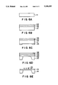
- FIGS. 3A-3I to 9A-9F are views to explain processes of preparing the X-ray mask structure of the present invention.
- the X-ray mask structure of the present invention is mainly characterized in that the X-ray transmissive membrane has a layer comprising aluminum nitride, and a nitride of heavy metal is used as the X-ray absorber. Having such constitution, the X-ray mask structure of the present invention can maintain a durability or endurance high enough to protect against, in particular, the expansion and shrinkage of the whole mask structure, caused by the exposure to X-rays repeated a thousand times or as many as several ten thousand times in practical use, and the vibration of the X-ray transmissive membrane and the X-ray absorber, caused by the pressure variations also repeated a thousand times or as many as several ten thousand times.
- the X-ray transmissive membrane mainly composed of aluminum and nitrogen has a low coefficient of thermal expansion and also has a high thermal conductivity.
- aluminum nitride (Al-N) shows a coefficient of thermal expansion of 4.3 ppm/° C. and a thermal conductivity of 260 W/m.K.
- This coefficient of thermal expansion is substantially the same value as that of the silicon wafer commonly preferably used as a substrate on which a conductive pattern is printed, and the thermal conductivity is much better than that of the silicon nitride (17 to 30 W/m.K) widely used in the X-ray transmissive membrane. Thus, it becomes possible to prevent the temperature elevation due to X-ray absorption.
- the aluminum nitride (the X-ray transmissive membrane) and the nitride of heavy metal (the X-ray absorber) are in optimum combination from the viewpoint of the adhesion between both.
- FIGS. 1A to 1D and FIGS. 2A to 2E are cross sectional views each illustrating the constitution of the X-ray mask structure of the present invention.
- the numeral 1 denotes a holding frame; numeral 2 denotes an X-ray transmissive membrane; and numeral 3 denotes an X-ray absorber.
- the X-ray transmissive membrane 2 is composed of aluminum nitride. Molar ratio (N/Al) of aluminum (Al) to Nitrogen (N) should preferably range from 0.3 to 1.5, and more preferably from 0.7 to 1.0. More specifically, a molar ratio of more than 1.5 may result in decreasing the transmittance of X-rays, and a molar ratio of less than 0.3 makes it difficult to control the internal stress. Moreover, a molar ratio outside the range of from 0.3 to 1.5 may also result in decreasing the practical durability previously mentioned.
- the X-ray transmissive membrane 2 may usually have a film thickness of from 0.5 ⁇ m to 5 ⁇ m.
- the X-ray absorber 3 is composed of the nitride of heavy metal.
- the heavy metal W, Ta, Hf, Mo, Nb, Zr, Ni, Ti, Rh, Ge, Ga, or alloys of these can be used.
- Ta, W, Hf can be preferably used.
- Molar ratio x of the heavy metal to nitrogen may preferably be in the range of 0 ⁇ x ⁇ 1.0, and more preferably 0.01 ⁇ x ⁇ 0.5. More specifically, a molar ratio of 0 makes it difficult to control the internal stress, and a molar ratio of more than 1.0 may cause a lowering in the ability of X-ray absorption.
- the X-ray absorber 3 may usually have a film thickness of from 0.02 ⁇ m to 5 ⁇ m.
- the X-ray transmissive membrane 2 and the X-ray absorber 3 described above may preferably be laminated in direct contact with each other from the viewpoint of the practical durability previously mentioned.
- the holding frame 1 holds thereon the X-ray transmissive membrane 2 and the X-ray absorber 3. It may usually be composed of a material such as Pyrex glass, Ti, or an Ti alloy.
- the X-ray transmissive membrane 2 may also be composed of the layer 2a of aluminum nitride and the protective layer 2b.
- the layer 2 of aluminum nitride and the X-ray absorber 3 may preferably be laminated in direct contact with each other from the view point of the practical durability previously mentioned.
- This protective layer 2b has a function of further improving the practical durability previously mentioned.
- Organic materials such as polyimide, polyamide, polyester and polyparaxylylene or inorganic materials such as Be, Ti, Si and B can be used for the protective layer 2b, but the organic materials are preferred.
- the protective layer should have a film thickness from 0.5 ⁇ m to 3 ⁇ m.
- the X-ray mask structure of the present invention is mainly characterized by the constitution as described above.
- FIGS. 2A to 2E show another embodiment of the present invention, particularly preferred from the viewpoint of the practical durability previously mentioned. More specifically, this embodiment is additionally characterized in that, in the X-ray mask structure previously shown in FIGS. 1A to 1D, the X-ray mask structure is provided between the X-ray transmissive membrane 2 and the X-ray absorber 3 with the intermediate layer 5 mainly composed of aluminum, a heavy metal and nitrogen.
- this intermediate layer 5 may be formed only between the X-ray mask structure 2 and the X-ray absorber 3.
- FIG. 2B shows, it may also be formed over the whole surface of the X-ray transmissive membrane 2 on the side on which the X-ray absorber 3 is provided.
- the structure shown in FIG. 2B can be obtained when the etching of the X-ray absorber is stopped in mid course, and the structure shown in FIG. 2A can be obtained when the etching is completely carried out in the process of making the X-ray mask structure.
- the difference in structure can be made only by changing processing conditions (in particular, the etching time).
- the structure shown in FIG. 2A is more advantageous in view of the fact that the transmittance of the visible light used in the mask alignment in X-ray lithography can be remarkably improved.
- compositional ratio of aluminum, a heavy metal and nitrogen in the intermediate layer 5 may preferably be set to be 1:3 to 0.001:5 to 0.3. This is particularly desirable from the viewpoint of durability.
- the intermediate layer 5 may preferably have a film thickness from 0.01 ⁇ m to 3 ⁇ m from the viewpoint of the practical durability previously mentioned.
- the protective layer 2b having a function previously mentioned may be provided as a part of the X-ray transmissive membrane 2.
- the intermediate layer 5 may be preferably laminated in direct contact with both the layer 2 of aluminum nitride and the X-ray absorber 3. This is preferred from the viewpoint of the practical durability previously mentioned.
- the X-ray mask structure of the present invention has been detailed in the above.
- a sub-layer for controlling stress or for processing may also be interposed between the holding frame and the X-ray transmissive membrane.
- the layer can be prepared by conventional methods, without any particular limitations.
- the X-ray mask structure of the present invention as described above is improved in that the X-ray transmission of the X-ray transmissive membrane, causes less strain in the X-ray transmissive membrane and the X-ray absorber when they are prepared and exposed to X-rays, and also in improved adhesion between the X-ray transmissive membrane and the X-ray absorber, so that it becomes possible to transfer patterns with high accuracy and also the X-ray absorber can be protected against collapse when it is prepared or used.
- an X-ray mask structure that has a durability high enough to protect even against the pattern exposure repeated a thousand times or as many as several ten thousand times to the same X-ray mask structure and the pressure variations repeated a thousand times or as many as several ten thousand times to the same X-ray mask structure, and does not cause any changes (deterioration) in the resolution of patterns with time.
- the Apiezon wax (a product of Shell Chemical Co.) layer 34 was formed (FIG. 3C), and, using this layer as a resist layer, the middle area of the thermally oxidized film 32 (a sub-layer) was removed using a mixed solution of ammonium fluoride and hydrofluoric acid (FIG. 3D).
- the middle area of the silicon wafer 31 was etched using an aqueous potassium hydroxide (KOH) solution so that the thermally oxidized film 32 was uncovered (FIG. 3F).
- KOH potassium hydroxide
- the thermally oxidized film 32 was then subjected to chemical dry etching to be removed under conditions of CF 4 : 20 SCCM, a gas pressure of 1.2 ⁇ 10 -1 Torr and a discharge electric power of 680 W (FIG. 3G).
- the processed wafer with the aluminum nitride film 33 on the surface was set in a sputtering apparatus.
- the silicon-containing resist 37 was further formed thereon with a thickness of 0.2 ⁇ m (FIG. 3H).
- the silicon-containing resist 37 was subjected to patterning by EB drawing to give a 0.25 ⁇ m line-and-space pattern. Subsequently, the resulting pattern was transferred to the polyimide film by reactive-ion etching using oxygen gas.
- the tungsten nitride film 35 was etched by reactive-ion etching using CF 4 +O 2 gas, under conditions of a gas pressure of 1.0 Pa and an RF power of 0.2 W/cm 2 to form the pattern 38 of the tungsten nitride film 35.
- the X-ray mask structure of the present invention was thus obtained (FIG. 3I).
- the silicon nitride film 32 of 2 ⁇ m thick was formed by LPCVD (FIG. 3A).
- Al(CH 3 ) 3 trimethylaluminum
- NH 3 ammonia
- the negative resist (OMR-83; a product of Tokyo Ohka Kogyo Co., Ltd.) layer 34 was formed in the shape of a ring (FIG. 3C), and, using this layer as a resist layer, the middle area of the silicon nitride film 32 was removed using a mixed solution of ammonium fluoride and hydrofluoric acid (FIG. 3D), followed by removal of the resist using a remover solution exclusively used therefor (FIG. 3E).
- the silicon wafer 31 was etched from the back using a mixed solution of hydrofluoric acid and nitric acid (FIG. 3F).
- the silicon nitride film thus uncovered was then subjected to chemical dry etching to be removed under conditions of CF 4 : 20 SCCM, a gas pressure of 1.2 ⁇ 10 -1 Torr and a discharge electric power of 680 W (FIG. 3G).
- the polyimide layer 36 was subsequently formed on the tantalum nitride film 35 to have a thickness of 1 ⁇ m. Then the silicon-containing resist 37 was further formed thereon with a thickness of 0.2 ⁇ m (FIG. 3H).
- the silicon-containing resist 37 was subjected to patterning by EB drawing to give a 0.25 ⁇ m line-and-space pattern. Subsequently, the resulting pattern was transferred to the polyimide film by reactive-ion etching using oxygen gas. Using this pattern as a mask, the tantalum nitride film 35 was etched by reactive-ion etching using Cl 2 gas, under conditions of a gas pressure of 1.0 Pa and an RF power of 0.2 W/cm 2 to form the pattern 38 of tantalum nitride. The X-ray mask structure of the present invention was thus obtained (FIG. 3I).
- the silicon oxide film 32 of 2 ⁇ m thick was formed by the thermal oxidation process (FIG. 3A).
- AlCl 3 aluminum chloride
- the negative resist 34 (AZ-1370; a product of Hoechst Ltd.) was formed in the shape of a ring (FIG. 3C), and, using this layer as a resist layer, the middle area of the thermally oxidized film 32 was removed using a mixed solution of ammonium fluoride and hydrofluoric acid (FIG. 3D), followed by removal of the resist using a remover solution exclusively used therefor (FIG. 3E).
- the processed wafer with the resulting aluminum nitride film was then set in a sputtering apparatus.
- the chromium (Cr) layer 36 was subsequently formed on the tungsten nitride film 35 by EB vacuum deposition to have a thickness of 500 ⁇ . Then the polymethyl methacrylate (PMMA) resist 37 was further formed thereon with a thickness of 1 ⁇ m (FIG. 3H).
- the polymethyl methacrylate resist 37 was subjected to patterning by EB drawing to give a 0.25 ⁇ m line-and-space pattern.
- the chromium layer 36 was etched by reactive-ion etching using chlorine gas, thus a pattern transfer was effected.
- the tungsten nitride film 35 was subjected to patterning by reactive-ion etching using sulfur hexafluoride (SF6) gas, followed by chemical dry etching from the back to remove the silicon oxide.
- SF6 sulfur hexafluoride
- Example 4 was carried out with the same manner in Example 3, except that the tungsten nitride film in Example 3 was replaced by a hafnium nitride (Hf-N) film.
- the X-ray mask structure of the present invention was thus obtained.
- the silicon wafer 41 (FIG. 4A) was set in a sputtering apparatus.
- the silicon-containing resist 45 was subjected to patterning by EB drawing to give a 0.25 ⁇ m line-and-space pattern. Subsequently, the resulting pattern was transferred to the polyimide film by reactive-ion etching using oxygen gas.
- the tungsten nitride film 43 was etched by reactive-ion etching using CF 4 +O 2 gas, under conditions of a gas pressure of 1.0 Pa and an RF power of 0.2 W/cm 2 to form a pattern 46 of the tungsten nitride film (FIG. 4D).
- the processed wafer with the aluminum nitride film 53 on the surface was set in a sputtering apparatus.
- the silicon-containing resist 56 was further formed thereon with a thickness of 0.2 ⁇ m (FIG. 5C).
- the silicon-containing resist 56 was subjected to patterning by EB drawing to give a 0.25 ⁇ m line-and-space pattern. Subsequently, the resulting pattern was transferred to the polyimide film 55 by reactive-ion etching using oxygen gas.
- the tungsten nitride film 54 was etched by reactive-ion etching using CF 4 +O 2 gas, under conditions of a gas pressure of 1.0 Pa and an RF power of 0.2 W/cm 2 to form the pattern 57 of the tungsten nitride film (FIG. 5D).
- the X-ray mask structure of the present invention as shown in FIG. 5E, having the polyimide layer as the protective layer, was thus obtained.
- a protective layer made of polyimide was further formed with a thickness of 2 ⁇ m.
- the X-ray mask structure of the present invention as shown in FIG. 1B, was thus obtained.
- a protective layer made of polyimide was further formed with a thickness of 1 ⁇ m.
- the X-ray mask structure of the present invention as shown in FIG. 1D, was thus obtained.
- the silicon wafer 61 was set in a sputtering apparatus having three types of targets: an aluminum nitride (Al-N) target, a mixed target of aluminum nitride (Al-N) and tungsten nitride (W-N) and a tungsten nitride (W-N) target (FIG. 6A).
- Al-N aluminum nitride
- Al-N mixed target of aluminum nitride
- W-N tungsten nitride
- W-N tungsten nitride
- Al-W-N Al-W-N layer 63
- the Apiezon wax (a product of Shell Chemical Co.) layer 65 was formed (FIG. 6C), and, using this layer as a resist layer, the middle area of the silicon wafer 61 was etched using an aqueous KOH solution.
- the polyimide layer 65 was formed on the tungsten nitride film 64 to have a thickness of 1 ⁇ m. Then the silicon-containing resist 66 was further formed thereon with a thickness of 0.2 ⁇ m (FIG. 6D).
- the silicon-containing resist 66 was subjected to patterning by electron beam (EB) drawing to give a 0.25 ⁇ m line-and-space pattern. Subsequently, the resulting pattern was transferred to the polyimide film by reactive-ion etching (RIE) using oxygen (O 2 ) gas.
- RIE reactive-ion etching
- the tungsten nitride film 64 and the Al-W-N layer 63 were etched by reactive-ion etching using CF 4 +O 2 gas, under conditions of a gas pressure of 1.0 Pa and a discharge electric power of 0.2 W/cm 2 to form the tungsten nitride film 68 and the Al-W-N layer (the intermediate layer) 67.
- the X-ray mask structure of the present invention was thus obtained (FIG. 6E).
- the silicon nitride film 72 of 0.2 ⁇ m thick was formed by the low-pressure chemical vapor deposition (LPCVD) process (FIG. 7A).
- Al(CH 3 ) 3 trimethylaluminum
- H 2 hydrogen
- NH 3 ammonia
- the negative resist (OMR-83; a product of Tokyo Ohka Kogyo Co., Ltd.) layer 74 was formed in the shape of a ring (FIG. 7C), and, using this layer as a resist layer, the middle area of the silicon nitride film 72 was removed using a mixed solution of ammonium fluoride and hydrofluoric acid (FIG. 7D), followed by removal of the resist layer 74 using a remover solution exclusively used therefor (FIG. 7E).
- the silicon wafer 71 was etched from the back, using a mixed solution of hydrofluoric acid and nitric acid (FIG. 7F).
- the silicon nitride film thus uncovered was then subjected to chemical dry etching for its removal under conditions of CF 4 : 20 SCCM, a gas pressure of 1.2 ⁇ 10 -1 Torr and a discharge electric power of 680 W (FIG. 7G).
- Ta-N tantalum nitride
- the polyimide layer 77 was subsequently formed on the tantalum nitride film 76 to have a thickness of 1 ⁇ m. Then the silicon-containing resist 78 was further formed thereon with a thickness of 0.2 ⁇ m (FIG. 7H).
- the silicon-containing resist 78 was subjected to patterning by EB drawing to give a 0.25 ⁇ m line-and-space pattern.
- the resulting pattern was subsequently transferred to the polyimide film by reactive-ion etching using oxygen gas.
- the tantalum nitride film was etched by reactive-ion etching using trifluorobromomethane (CBrF 3 ) gas, under conditions of a gas pressure of 5 ⁇ 10 -3 Torr and a discharge electric power of 0.3 W/cm 2 to form the pattern 79 of the tantalum nitride film.
- CBrF 3 trifluorobromomethane
- AlCl 3 aluminum chloride
- NH 3 ammonia
- tungsten nitride (W-N) target was carried out under the same conditions to form the tungsten nitride (W-N) film 94 of 0.8 ⁇ m thick (FIG. 9C).
- the Cr layer 95 was further formed by deposition with a thickness of 500 ⁇ in Ar gas.
- the polymethyl methacrylate (PMMA; OEBR-1000; a product of Tokyo Ohka Kogyo Co., Ltd.) resist layer 96 was formed on the Cr layer 95 to have a thickness of 1 ⁇ m (FIG. 9D).
- the PMMA resist layer 96 was then subjected to patterning by EB drawing to give a 0.25 ⁇ m line-and-space pattern. Subsequently, using the resulting PMMA pattern as a mask, the Cr layer 95 was etched by reactive-ion etching using Cl 2 gas to transfer the pattern.
- the tungsten nitride (W-N) film 94 was subjected to patterning using SF 6 to form the absorber pattern 98 (FIG. 9E). Thereafter, the middle area of the silicon wafer 91 was etched from the back using an aqueous KOH solution. The X-ray mask structure of the present invention was thus obtained (FIG. 9F).
- a protective layer made of polyimide was further formed with a thickness of 2.5 ⁇ m.
- the X-ray mask structure of the present invention as shown in FIG. 2C, was thus obtained.
- a protective layer made of polyimide was further formed with a thickness of 1.5 ⁇ m.
- the X-ray mask structure of the present invention as shown in FIG. 2E, was thus obtained.
- the silicon wafer 81, on which the polyimide layer 82 serving as a protective layer had been formed with a thickness of 2 ⁇ m (FIG. 8A), was set in a sputtering apparatus.
- Al-N aluminum nitride
- W-N tungsten nitride
- the polyimide film 86 was further formed on the film 85 to have a thickness of 1 ⁇ m, and the silicon-containing resist 87 was further formed thereon with a thickness of 0.2 ⁇ m (FIG. 8C).
- the silicon-containing resist 87 was then subjected to patterning by EB drawing to give a 0.25 ⁇ m line-and-space pattern. Subsequently, the resulting pattern was transferred to the polyimide film 86 by reactive-ion etching using oxygen gas.
- the tungsten nitride film 85 and the Al-W-N layer 84 were etched.
- the tungsten nitride film 85 was etched by reactive-ion etching using CF 4 +O 2 gas under conditions of a gas pressure of 1.0 Pa and an RF power of 0.2 W/cm 2
- the Al-W-N layer 84 was etched under the same conditions except for the addition of Cl 2 gas, to form patterns (88 and 89) comprising tungsten nitride and Al-W-N (FIG. 8D).
- the X-ray mask structure of the present invention having the polyimide layer 82 as the protective layer, was thus obtained (FIG. 8E).
- Example 11 was repeated to prepare an X-ray mask structure, except that the tungsten nitride layer was replaced with a tungsten layer and the Al-W-N layer was not provided.
- the X-ray mask structures prepared in Examples 1 to 14 were each set on the surface of a silicon wafer (the exposing object) coated with a resist material (RAY-PF; a product of Hoechst Ltd.), which was then exposed to light to form a mask (absorber) pattern on the exposing object, using soft X-rays with a wavelength of 1 nm, taken out by spectroscopy of SOR light.
- a resist material RAUY-PF; a product of Hoechst Ltd.
- the amount of exposure was so controlled as to be 75 mJ/cm 2 on the silicon wafer, and the exposure was carried out in an atmosphere of He gas under a pressure of 150 Torr.
- the X-ray mask structures prepared in Examples 1 to 14 and Comparative Examples 1 and 2 were each set on the surface of the same silicon wafer (the exposing object) as that used in Example 15, which was then exposed to light to form a mask (absorber) pattern on the exposing object under the same conditions as in Example 15, provided that X-rays were irradiated for 10 seconds for each one shot, and this was repeated 10,000 times on the same X-ray mask structure.
- the pressure of the exposure atmosphere was also returned to atmospheric pressure every time when the above one shot of X-ray irradiation was completed.
- Results obtained are shown in Table 1.
- evaluation was made based on the amount of change ( ⁇ x) between the transferred pattern width ( ⁇ m) on the silicon wafer obtained by the first exposure of X-ray and the transferred pattern width ( ⁇ m) on the silicon wafer obtained by the exposure of X-ray, at number of shots of 100, 500, 1,000, 5,000 and 10,000.
Landscapes
- Physics & Mathematics (AREA)
- General Physics & Mathematics (AREA)
- Exposure Of Semiconductors, Excluding Electron Or Ion Beam Exposure (AREA)
- Preparing Plates And Mask In Photomechanical Process (AREA)
Priority Applications (1)
| Application Number | Priority Date | Filing Date | Title |
|---|---|---|---|
| US08/565,215 US5773177A (en) | 1989-03-09 | 1995-11-30 | X-ray mask structure, and X-ray exposure process |
Applications Claiming Priority (6)
| Application Number | Priority Date | Filing Date | Title |
|---|---|---|---|
| JP5503189 | 1989-03-09 | ||
| JP1-55031 | 1989-03-09 | ||
| JP2-41110 | 1990-02-23 | ||
| JP4111090A JP2684105B2 (ja) | 1990-02-23 | 1990-02-23 | X線マスク構造体及びそれを用いたx線露光方法 |
| JP2-47238 | 1990-03-01 | ||
| JP2047238A JPH0316116A (ja) | 1989-03-09 | 1990-03-01 | X線リソグラフィー用マスク構造体及びそれを用いたx線露光方法 |
Related Child Applications (1)
| Application Number | Title | Priority Date | Filing Date |
|---|---|---|---|
| US94028692A Division | 1989-03-09 | 1992-09-03 |
Publications (1)
| Publication Number | Publication Date |
|---|---|
| US5196283A true US5196283A (en) | 1993-03-23 |
Family
ID=27290709
Family Applications (2)
| Application Number | Title | Priority Date | Filing Date |
|---|---|---|---|
| US07/489,277 Expired - Fee Related US5196283A (en) | 1989-03-09 | 1990-03-06 | X-ray mask structure, and x-ray exposure process |
| US08/565,215 Expired - Fee Related US5773177A (en) | 1989-03-09 | 1995-11-30 | X-ray mask structure, and X-ray exposure process |
Family Applications After (1)
| Application Number | Title | Priority Date | Filing Date |
|---|---|---|---|
| US08/565,215 Expired - Fee Related US5773177A (en) | 1989-03-09 | 1995-11-30 | X-ray mask structure, and X-ray exposure process |
Country Status (3)
| Country | Link |
|---|---|
| US (2) | US5196283A (de) |
| EP (1) | EP0386786B1 (de) |
| DE (1) | DE69023023T2 (de) |
Cited By (27)
| Publication number | Priority date | Publication date | Assignee | Title |
|---|---|---|---|---|
| US5335256A (en) * | 1991-03-18 | 1994-08-02 | Canon Kabushiki Kaisha | Semiconductor substrate including a single or multi-layer film having different densities in the thickness direction |
| US5396066A (en) * | 1992-07-06 | 1995-03-07 | Canon Kabushiki Kaisha | Displacement element, cantilever probe and information processing apparatus using cantilever probe |
| US5422921A (en) * | 1991-11-15 | 1995-06-06 | Canon Kabushiki Kaisha | X-ray mask structure and manufacturing methods including forming a metal oxide film on a portion of an X-ray permeable film having no X-ray absorber thereon |
| US5496667A (en) * | 1992-06-08 | 1996-03-05 | Mitsubishi Denki Kabushiki Kaisha | X-ray mask and its fabrication method |
| US5512395A (en) * | 1993-04-30 | 1996-04-30 | Lsi Logic Corporation | Image masks for semiconductor lithography |
| US5572562A (en) * | 1993-04-30 | 1996-11-05 | Lsi Logic Corporation | Image mask substrate for X-ray semiconductor lithography |
| US5754619A (en) * | 1996-01-09 | 1998-05-19 | Nec Corporation | X-ray mask for X-ray lithography and method of producing same |
| US5773177A (en) * | 1989-03-09 | 1998-06-30 | Canon Kabushiki Kaisha | X-ray mask structure, and X-ray exposure process |
| US6066418A (en) * | 1996-07-10 | 2000-05-23 | Nec Corporation | X-ray mask and fabrication process therefor |
| US6297169B1 (en) * | 1998-07-27 | 2001-10-02 | Motorola, Inc. | Method for forming a semiconductor device using a mask having a self-assembled monolayer |
| US6610447B2 (en) * | 2001-03-30 | 2003-08-26 | Intel Corporation | Extreme ultraviolet mask with improved absorber |
| US20040178170A1 (en) * | 2002-12-16 | 2004-09-16 | Kenichi Morimoto | Mask blank for charged particle beam exposure, method of forming mask blank and mask for charged particle beam exposure |
| US20050118835A1 (en) * | 2003-10-02 | 2005-06-02 | Asml Netherlands B.V. | Lithographic projection apparatus, mirror, method of supplying a protective cap layer, device manufacturing method and device manufactured accordingly |
| KR100505014B1 (ko) * | 2002-11-14 | 2005-08-01 | 전자부품연구원 | X-선 마스크 및 그 제조방법 |
| US8247971B1 (en) | 2009-03-19 | 2012-08-21 | Moxtek, Inc. | Resistively heated small planar filament |
| US8750458B1 (en) | 2011-02-17 | 2014-06-10 | Moxtek, Inc. | Cold electron number amplifier |
| US8761344B2 (en) | 2011-12-29 | 2014-06-24 | Moxtek, Inc. | Small x-ray tube with electron beam control optics |
| US8804910B1 (en) | 2011-01-24 | 2014-08-12 | Moxtek, Inc. | Reduced power consumption X-ray source |
| US8929515B2 (en) | 2011-02-23 | 2015-01-06 | Moxtek, Inc. | Multiple-size support for X-ray window |
| US8948345B2 (en) | 2010-09-24 | 2015-02-03 | Moxtek, Inc. | X-ray tube high voltage sensing resistor |
| US8964943B2 (en) | 2010-10-07 | 2015-02-24 | Moxtek, Inc. | Polymer layer on X-ray window |
| US8989354B2 (en) | 2011-05-16 | 2015-03-24 | Brigham Young University | Carbon composite support structure |
| US9076628B2 (en) | 2011-05-16 | 2015-07-07 | Brigham Young University | Variable radius taper x-ray window support structure |
| US9173623B2 (en) | 2013-04-19 | 2015-11-03 | Samuel Soonho Lee | X-ray tube and receiver inside mouth |
| US9174412B2 (en) | 2011-05-16 | 2015-11-03 | Brigham Young University | High strength carbon fiber composite wafers for microfabrication |
| US9207529B2 (en) | 2012-12-27 | 2015-12-08 | Asahi Glass Company, Limited | Reflective mask blank for EUV lithography, and process for its production |
| US9305735B2 (en) | 2007-09-28 | 2016-04-05 | Brigham Young University | Reinforced polymer x-ray window |
Families Citing this family (7)
| Publication number | Priority date | Publication date | Assignee | Title |
|---|---|---|---|---|
| KR100244458B1 (ko) * | 1997-03-26 | 2000-03-02 | 김영환 | 마스크 및 그 제조방법 |
| US6365326B1 (en) | 1999-05-07 | 2002-04-02 | International Business Machines Corporation | Pattern density tailoring for etching of advanced lithographic mask |
| DE10004394A1 (de) * | 2000-02-02 | 2001-08-16 | Infineon Technologies Ag | Verfahren zur Grabenätzung in Halbleitermaterial |
| US6537706B1 (en) * | 2000-03-14 | 2003-03-25 | Intel Corporation | Method for making a photolithographic mask |
| US9938616B2 (en) * | 2014-07-29 | 2018-04-10 | Lam Research Corporation | Physical vapor deposition of low-stress nitrogen-doped tungsten films |
| US20230287555A1 (en) * | 2022-03-10 | 2023-09-14 | Abdulilah Mayet | Micro-electromechanical system (mems) based inertial sensor and method of fabrication thereof |
| DE102022118318A1 (de) * | 2022-07-21 | 2024-02-01 | Jenoptik Optical Systems Gmbh | Verfahren und Vorrichtung zur Herstellung eines Bauelementes mit wenigstens einem Membranabschnitt und Bauelement und Verwendung eines Bauelements |
Citations (11)
| Publication number | Priority date | Publication date | Assignee | Title |
|---|---|---|---|---|
| JPS61118754A (ja) * | 1984-11-15 | 1986-06-06 | Canon Inc | X線リソグラフイ−法及びx線リソグラフイ−用マスク保持体 |
| JPS6280656A (ja) * | 1985-10-04 | 1987-04-14 | Toppan Printing Co Ltd | フオトマスクブランクおよびフオトマスク |
| US4677042A (en) * | 1984-11-05 | 1987-06-30 | Canon Kabushiki Kaisha | Mask structure for lithography, method for preparation thereof and lithographic method |
| US4735877A (en) * | 1985-10-07 | 1988-04-05 | Canon Kabushiki Kaisha | Lithographic mask structure and lithographic process |
| JPS6376325A (ja) * | 1987-06-30 | 1988-04-06 | Agency Of Ind Science & Technol | X線リソグラフィ−用マスクのx線吸収体膜 |
| JPS6376872A (ja) * | 1986-09-18 | 1988-04-07 | Agency Of Ind Science & Technol | 膜の内部圧縮応力低減方法 |
| JPS63232425A (ja) * | 1987-03-20 | 1988-09-28 | Mitsubishi Electric Corp | X線露光用マスクおよびその製造方法 |
| JPS63317676A (ja) * | 1987-06-19 | 1988-12-26 | Sharp Corp | 無粒構造金属化合物薄膜の製造方法 |
| US4804600A (en) * | 1984-07-06 | 1989-02-14 | Canon Kabushiki Kaisha | Lithographic mask structure and process for preparing the same |
| US4837123A (en) * | 1985-01-07 | 1989-06-06 | Canon Kabushiki Kaisha | Mask structure for lithography, method of preparation thereof and lithographic method |
| US5012500A (en) * | 1987-12-29 | 1991-04-30 | Canon Kabushiki Kaisha | X-ray mask support member, X-ray mask, and X-ray exposure process using the X-ray mask |
Family Cites Families (9)
| Publication number | Priority date | Publication date | Assignee | Title |
|---|---|---|---|---|
| US4235877A (en) * | 1979-06-27 | 1980-11-25 | Merck & Co., Inc. | Liposome particle containing viral or bacterial antigenic subunit |
| JPS61126551A (ja) * | 1984-11-26 | 1986-06-14 | Canon Inc | X線リソグラフイ−用マスク構造体の製造方法 |
| JPS63139352A (ja) * | 1986-12-02 | 1988-06-11 | Mitsubishi Paper Mills Ltd | 印刷版用修正液 |
| JPH0681728B2 (ja) * | 1987-10-02 | 1994-10-19 | 株式会社上野製薬応用研究所 | 下 剤 |
| JP2742056B2 (ja) * | 1988-06-14 | 1998-04-22 | 富士通株式会社 | X線マスク |
| US5005075A (en) * | 1989-01-31 | 1991-04-02 | Hoya Corporation | X-ray mask and method of manufacturing an X-ray mask |
| US5196283A (en) * | 1989-03-09 | 1993-03-23 | Canon Kabushiki Kaisha | X-ray mask structure, and x-ray exposure process |
| JP2823276B2 (ja) * | 1989-03-18 | 1998-11-11 | 株式会社東芝 | X線マスクの製造方法および薄膜の内部応力制御装置 |
| US5193283A (en) * | 1992-07-27 | 1993-03-16 | Alex Hsiao | Bicycle wheel spike inpecting and adjusting device |
-
1990
- 1990-03-06 US US07/489,277 patent/US5196283A/en not_active Expired - Fee Related
- 1990-03-09 DE DE69023023T patent/DE69023023T2/de not_active Expired - Fee Related
- 1990-03-09 EP EP90104540A patent/EP0386786B1/de not_active Expired - Lifetime
-
1995
- 1995-11-30 US US08/565,215 patent/US5773177A/en not_active Expired - Fee Related
Patent Citations (11)
| Publication number | Priority date | Publication date | Assignee | Title |
|---|---|---|---|---|
| US4804600A (en) * | 1984-07-06 | 1989-02-14 | Canon Kabushiki Kaisha | Lithographic mask structure and process for preparing the same |
| US4677042A (en) * | 1984-11-05 | 1987-06-30 | Canon Kabushiki Kaisha | Mask structure for lithography, method for preparation thereof and lithographic method |
| JPS61118754A (ja) * | 1984-11-15 | 1986-06-06 | Canon Inc | X線リソグラフイ−法及びx線リソグラフイ−用マスク保持体 |
| US4837123A (en) * | 1985-01-07 | 1989-06-06 | Canon Kabushiki Kaisha | Mask structure for lithography, method of preparation thereof and lithographic method |
| JPS6280656A (ja) * | 1985-10-04 | 1987-04-14 | Toppan Printing Co Ltd | フオトマスクブランクおよびフオトマスク |
| US4735877A (en) * | 1985-10-07 | 1988-04-05 | Canon Kabushiki Kaisha | Lithographic mask structure and lithographic process |
| JPS6376872A (ja) * | 1986-09-18 | 1988-04-07 | Agency Of Ind Science & Technol | 膜の内部圧縮応力低減方法 |
| JPS63232425A (ja) * | 1987-03-20 | 1988-09-28 | Mitsubishi Electric Corp | X線露光用マスクおよびその製造方法 |
| JPS63317676A (ja) * | 1987-06-19 | 1988-12-26 | Sharp Corp | 無粒構造金属化合物薄膜の製造方法 |
| JPS6376325A (ja) * | 1987-06-30 | 1988-04-06 | Agency Of Ind Science & Technol | X線リソグラフィ−用マスクのx線吸収体膜 |
| US5012500A (en) * | 1987-12-29 | 1991-04-30 | Canon Kabushiki Kaisha | X-ray mask support member, X-ray mask, and X-ray exposure process using the X-ray mask |
Non-Patent Citations (2)
| Title |
|---|
| T. Kanayma et al. "Reduction in X-ray Mass Distortion Using Amorphous WN Absorber Stress Compensated with Ion Bombardment", Journal of Vacuum Science and Technoloy, Part B, vol. 6, No. 1, pp. 174-177, Feb. 1988 New York. |
| T. Kanayma et al. Reduction in X ray Mass Distortion Using Amorphous WN Absorber Stress Compensated with Ion Bombardment , Journal of Vacuum Science and Technoloy, Part B, vol. 6, No. 1, pp. 174 177, Feb. 1988 New York. * |
Cited By (33)
| Publication number | Priority date | Publication date | Assignee | Title |
|---|---|---|---|---|
| US5773177A (en) * | 1989-03-09 | 1998-06-30 | Canon Kabushiki Kaisha | X-ray mask structure, and X-ray exposure process |
| US5335256A (en) * | 1991-03-18 | 1994-08-02 | Canon Kabushiki Kaisha | Semiconductor substrate including a single or multi-layer film having different densities in the thickness direction |
| US5422921A (en) * | 1991-11-15 | 1995-06-06 | Canon Kabushiki Kaisha | X-ray mask structure and manufacturing methods including forming a metal oxide film on a portion of an X-ray permeable film having no X-ray absorber thereon |
| US5496667A (en) * | 1992-06-08 | 1996-03-05 | Mitsubishi Denki Kabushiki Kaisha | X-ray mask and its fabrication method |
| US5396066A (en) * | 1992-07-06 | 1995-03-07 | Canon Kabushiki Kaisha | Displacement element, cantilever probe and information processing apparatus using cantilever probe |
| US5512395A (en) * | 1993-04-30 | 1996-04-30 | Lsi Logic Corporation | Image masks for semiconductor lithography |
| US5572562A (en) * | 1993-04-30 | 1996-11-05 | Lsi Logic Corporation | Image mask substrate for X-ray semiconductor lithography |
| US5754619A (en) * | 1996-01-09 | 1998-05-19 | Nec Corporation | X-ray mask for X-ray lithography and method of producing same |
| US6066418A (en) * | 1996-07-10 | 2000-05-23 | Nec Corporation | X-ray mask and fabrication process therefor |
| US6297169B1 (en) * | 1998-07-27 | 2001-10-02 | Motorola, Inc. | Method for forming a semiconductor device using a mask having a self-assembled monolayer |
| US6610447B2 (en) * | 2001-03-30 | 2003-08-26 | Intel Corporation | Extreme ultraviolet mask with improved absorber |
| US20030228530A1 (en) * | 2001-03-30 | 2003-12-11 | Pei-Yang Yan | Extreme ultraviolet mask with improved absorber |
| US6908714B2 (en) | 2001-03-30 | 2005-06-21 | Intel Corporation | Absorber layer for EUV |
| KR100505014B1 (ko) * | 2002-11-14 | 2005-08-01 | 전자부품연구원 | X-선 마스크 및 그 제조방법 |
| US20060124581A1 (en) * | 2002-12-16 | 2006-06-15 | Kenichi Morimoto | Mask blank for charged particle beam exposure, method of forming mask blank and mask for charged particle beam exposure |
| US20040178170A1 (en) * | 2002-12-16 | 2004-09-16 | Kenichi Morimoto | Mask blank for charged particle beam exposure, method of forming mask blank and mask for charged particle beam exposure |
| US7479233B2 (en) | 2002-12-16 | 2009-01-20 | Dai Nippon Printing Co., Ltd. | Mask blank for charged particle beam exposure, method of forming mask blank and mask for charged particle beam exposure |
| US7588815B2 (en) * | 2002-12-16 | 2009-09-15 | Dai Nippon Printing Co., Ltd. | Mask blank for charged particle beam exposure, method of forming mask blank and mask for charged particle beam exposure |
| US7420653B2 (en) * | 2003-10-02 | 2008-09-02 | Asml Netherlands B.V. | Lithographic projection apparatus, mirror, method of supplying a protective cap layer, device manufacturing method and device manufactured accordingly |
| US20050118835A1 (en) * | 2003-10-02 | 2005-06-02 | Asml Netherlands B.V. | Lithographic projection apparatus, mirror, method of supplying a protective cap layer, device manufacturing method and device manufactured accordingly |
| US9305735B2 (en) | 2007-09-28 | 2016-04-05 | Brigham Young University | Reinforced polymer x-ray window |
| US8247971B1 (en) | 2009-03-19 | 2012-08-21 | Moxtek, Inc. | Resistively heated small planar filament |
| US8948345B2 (en) | 2010-09-24 | 2015-02-03 | Moxtek, Inc. | X-ray tube high voltage sensing resistor |
| US8964943B2 (en) | 2010-10-07 | 2015-02-24 | Moxtek, Inc. | Polymer layer on X-ray window |
| US8804910B1 (en) | 2011-01-24 | 2014-08-12 | Moxtek, Inc. | Reduced power consumption X-ray source |
| US8750458B1 (en) | 2011-02-17 | 2014-06-10 | Moxtek, Inc. | Cold electron number amplifier |
| US8929515B2 (en) | 2011-02-23 | 2015-01-06 | Moxtek, Inc. | Multiple-size support for X-ray window |
| US8989354B2 (en) | 2011-05-16 | 2015-03-24 | Brigham Young University | Carbon composite support structure |
| US9076628B2 (en) | 2011-05-16 | 2015-07-07 | Brigham Young University | Variable radius taper x-ray window support structure |
| US9174412B2 (en) | 2011-05-16 | 2015-11-03 | Brigham Young University | High strength carbon fiber composite wafers for microfabrication |
| US8761344B2 (en) | 2011-12-29 | 2014-06-24 | Moxtek, Inc. | Small x-ray tube with electron beam control optics |
| US9207529B2 (en) | 2012-12-27 | 2015-12-08 | Asahi Glass Company, Limited | Reflective mask blank for EUV lithography, and process for its production |
| US9173623B2 (en) | 2013-04-19 | 2015-11-03 | Samuel Soonho Lee | X-ray tube and receiver inside mouth |
Also Published As
| Publication number | Publication date |
|---|---|
| EP0386786A3 (de) | 1991-05-02 |
| US5773177A (en) | 1998-06-30 |
| EP0386786B1 (de) | 1995-10-18 |
| DE69023023D1 (de) | 1995-11-23 |
| DE69023023T2 (de) | 1996-05-15 |
| EP0386786A2 (de) | 1990-09-12 |
Similar Documents
| Publication | Publication Date | Title |
|---|---|---|
| US5196283A (en) | X-ray mask structure, and x-ray exposure process | |
| EP1152292B1 (de) | Halbton-Phasenschiebermaske sowie Maskenrohling | |
| US5447598A (en) | Process for forming resist mask pattern | |
| US4722878A (en) | Photomask material | |
| US5389474A (en) | Mask for photolithography | |
| US5677111A (en) | Process for production of micropattern utilizing antireflection film | |
| EP1321820B1 (de) | Halbton-phasenverschiebungsfotomaske und rohling für eine halbton-phasenverschiebungsfotomaske | |
| EP0381467A1 (de) | Methode zur Herstellung einer Röntgenmaske | |
| US5464711A (en) | Process for fabricating an X-ray absorbing mask | |
| JPH0245927A (ja) | エッチング方法 | |
| US12591172B2 (en) | EUV transmissive membrane | |
| US6458496B2 (en) | Blank for halftone phase shift photomask and halftone phase shift photomask | |
| US20250278032A1 (en) | Euv transmissive membrane, processing method thereof, and exposure method | |
| CN118805142A (zh) | Euv透过膜的制造方法以及防护件 | |
| EP0260201B1 (de) | Plasma-Ätzverfahren unter Verwendung eines zweischichtigen Musters | |
| JP4641086B2 (ja) | ハーフトーン位相シフトフォトマスク用ブランクス、及びハーフトーン位相シフトフォトマスクとその製造方法 | |
| EP0518545A1 (de) | Lithographisches Trockenätzverfahren mittels Gasgemischen aus Sauerstoff und Chlor | |
| JP2684105B2 (ja) | X線マスク構造体及びそれを用いたx線露光方法 | |
| JPH0316116A (ja) | X線リソグラフィー用マスク構造体及びそれを用いたx線露光方法 | |
| JPH08272074A (ja) | ハーフトーン位相シフトフォトマスク及びハーフトーン位相シフトフォトマスク用ブランクス | |
| KR100248629B1 (ko) | 엑스레이 마스크의 형성 방법 | |
| JP2943217B2 (ja) | X線露光マスクとその製造方法 | |
| JPH05333528A (ja) | 反射型マスクおよびその製造方法 | |
| JPH04315417A (ja) | 長波長x線露光用マスク及びその製造方法 | |
| JPH0366656B2 (de) |
Legal Events
| Date | Code | Title | Description |
|---|---|---|---|
| AS | Assignment |
Owner name: CANON KABUSHIKI KAISHA, JAPAN Free format text: ASSIGNMENT OF ASSIGNORS INTEREST.;ASSIGNORS:IKEDA, TSUTOMU;SUGATA, MASAO;KATO, HIDEO;REEL/FRAME:005246/0903 Effective date: 19900301 |
|
| CC | Certificate of correction | ||
| FPAY | Fee payment |
Year of fee payment: 4 |
|
| FEPP | Fee payment procedure |
Free format text: PAYER NUMBER DE-ASSIGNED (ORIGINAL EVENT CODE: RMPN); ENTITY STATUS OF PATENT OWNER: LARGE ENTITY |
|
| FPAY | Fee payment |
Year of fee payment: 8 |
|
| REMI | Maintenance fee reminder mailed | ||
| LAPS | Lapse for failure to pay maintenance fees | ||
| STCH | Information on status: patent discontinuation |
Free format text: PATENT EXPIRED DUE TO NONPAYMENT OF MAINTENANCE FEES UNDER 37 CFR 1.362 |
|
| FP | Lapsed due to failure to pay maintenance fee |
Effective date: 20050323 |