US5402480A - Call signal generating circuit - Google Patents
Call signal generating circuit Download PDFInfo
- Publication number
- US5402480A US5402480A US07/931,000 US93100092A US5402480A US 5402480 A US5402480 A US 5402480A US 93100092 A US93100092 A US 93100092A US 5402480 A US5402480 A US 5402480A
- Authority
- US
- United States
- Prior art keywords
- call signal
- signal generating
- generating circuit
- coupled
- switching means
- Prior art date
- Legal status (The legal status is an assumption and is not a legal conclusion. Google has not performed a legal analysis and makes no representation as to the accuracy of the status listed.)
- Expired - Fee Related
Links
Images




Classifications
-
- H—ELECTRICITY
- H04—ELECTRIC COMMUNICATION TECHNIQUE
- H04M—TELEPHONIC COMMUNICATION
- H04M19/00—Current supply arrangements for telephone systems
- H04M19/02—Current supply arrangements for telephone systems providing ringing current or supervisory tones, e.g. dialling tone or busy tone
-
- H—ELECTRICITY
- H02—GENERATION; CONVERSION OR DISTRIBUTION OF ELECTRIC POWER
- H02M—APPARATUS FOR CONVERSION BETWEEN AC AND AC, BETWEEN AC AND DC, OR BETWEEN DC AND DC, AND FOR USE WITH MAINS OR SIMILAR POWER SUPPLY SYSTEMS; CONVERSION OF DC OR AC INPUT POWER INTO SURGE OUTPUT POWER; CONTROL OR REGULATION THEREOF
- H02M7/00—Conversion of AC power input into DC power output; Conversion of DC power input into AC power output
- H02M7/42—Conversion of DC power input into AC power output without possibility of reversal
- H02M7/44—Conversion of DC power input into AC power output without possibility of reversal by static converters
- H02M7/48—Conversion of DC power input into AC power output without possibility of reversal by static converters using discharge tubes with control electrode or semiconductor devices with control electrode
- H02M7/4807—Conversion of DC power input into AC power output without possibility of reversal by static converters using discharge tubes with control electrode or semiconductor devices with control electrode having a high frequency intermediate AC stage
-
- Y—GENERAL TAGGING OF NEW TECHNOLOGICAL DEVELOPMENTS; GENERAL TAGGING OF CROSS-SECTIONAL TECHNOLOGIES SPANNING OVER SEVERAL SECTIONS OF THE IPC; TECHNICAL SUBJECTS COVERED BY FORMER USPC CROSS-REFERENCE ART COLLECTIONS [XRACs] AND DIGESTS
- Y02—TECHNOLOGIES OR APPLICATIONS FOR MITIGATION OR ADAPTATION AGAINST CLIMATE CHANGE
- Y02D—CLIMATE CHANGE MITIGATION TECHNOLOGIES IN INFORMATION AND COMMUNICATION TECHNOLOGIES [ICT], I.E. INFORMATION AND COMMUNICATION TECHNOLOGIES AIMING AT THE REDUCTION OF THEIR OWN ENERGY USE
- Y02D30/00—Reducing energy consumption in communication networks
- Y02D30/70—Reducing energy consumption in communication networks in wireless communication networks
Definitions
- the present invention generally relates to call signal generating circuits, and more particularly to a call signal generating circuit which generates a call signal by carrying out a switching control.
- a call signal which is used to call and ring the bell of the telephone set from the switching system is also sometimes referred to as a ringing signal.
- a low-frequency signal of 16 Hz and 75 V is turned ON for one second and turned OFF for two seconds to form the call signal.
- the call signal is generated by a call signal generating circuit, and there is a demand to improve the characteristic and efficiency of the call signal generating circuit.
- the call signal was originally a sinusoidal wave, but the call signal was replaced by a staircase wave which approximates the crest factor of the sinusoidal wave.
- the voltage supplied from the switching system to the telephone set of the subscriber is 48 V.
- the call signal has the frequency of 16 Hz and the peak voltage of 75 V.
- a step-up transformer is used to boost the voltage when forming the call signal.
- the step-up transformer designed for the low-frequency of approximately 16 Hz is bulky, and the method of boosting the voltage using a high-frequency signal was conventionally used.
- FIG. 1 shows an example of a conventional call signal generating circuit.
- the conventional call signal generating circuit includes a transformer 41 having a primary winding 41a and secondary windings 41b and 41c, a transistor 42, a capacitor 43, diodes 44 and 45, photo-transistors 46 and 47, a capacitor 48, a control circuit 49, photodiodes 50 and 51, a dummy resistor 52 and output terminals 53 which are connected as shown in FIG.1.
- a D.C. voltage is applied to the primary winding 41a of the transformer 41 via the transistor 42, and this transistor 42 is turned ON/OFF at a frequency of several tens of kHz to several hundred kHz by the control circuit 49. Accordingly, compared to the case where the 16 Hz signal is boosted, it is possible to reduce the size of the transformer 41.
- the voltage of several tens of kHz to several hundred kHz induced at the secondary windings 41b and 41c of the transformer 41 due to the ON/OFF control of the transistor 42 is rectified by the diodes 44 and 45.
- the diode 44 rectifies the voltage into a positive polarity voltage
- the diode 45 rectifies the voltage into a negative polarity voltage.
- the phototransistors 46 and 47 are respectively turned ON/OFF by the voltages from the diodes 44 and 45, and the phototransistors 46 and 47 are turned ON/OFF alternately. Hence, a positive polarity voltage from the phototransistor 46 and a negative polarity voltage from the phototransistor 47 are output alternately, and a call signal of 16 Hz is output via the output terminals 53.
- a photo coupler is formed by the phototransistor 46 and the photodiode 50, and another photo coupler is formed by the phototransistor 47 and the photodiode 51.
- the photodiodes 50 and 51 are alternately driven by the control circuit 49 for a time which is shorter than one-half the period of the 16 Hz call signal. Accordingly, the phototransistors 46 and 47 are alternately turned ON with respective quiescent times.
- the capacitor 48 is provided to eliminate switching frequency components of several tens of kHz to several hundred kHz induced at the secondary windings 41b and 41c, other high-frequency components and the like.
- the dummy resistor 52 is provided to discharge the capacitor 48.
- FIG.2 is a time chart for explaining the operation of the conventional call signal generating circuit shown in FIG. 1.
- FIG. 2 shows a current supplied to the photodiode 50
- (b) shows a current supplied to the photodiode 51
- (c) and (d) show the call signal output via the output terminals 53.
- the photodiodes 50 and 51 receive the currents from the control circuit 49. If the 16 Hz call signal has a period T1, the current is supplied to the photodiode 50 for a time T2, the current is supplied to the photodiode 51 for a time T4 and quiescent times T3 and T5 are provided as shown in FIG.
- T1 T2+T3+T4+T5
- the crest factor of the sinusoidal signal which is equal to (crest value)/(effective value) is 1.414, and the quiescent times T3 and T5 are set so as to approximate this crest factor.
- the effective value is the average of the square of the instantaneous value of one period of the fundamental wave, and the crest value is the peak value of the wave.
- the phototransistors 46 and 47 When the currents are supplied to the photodiodes 50 and 51 which form the photo coupler with the respective phototransistors 46 and 47, the phototransistors 46 and 47 are turned ON by the light from the photodiodes 50 and 51 applied to the bases of the phototransistors 46 and 47.
- the phototransistors 46 and 47 are respectively turned ON during the times T2 and T4 in FIG. 2. As a result, it is possible to obtain the call signal which has the staircase waveform with the crest factor approximating the crest factor of the sinusoidal wave.
- the dummy resistor 52 is omitted and the call signal generating circuit assumes a low-load state, it becomes equivalent to the case where the discharge time constant of the capacitor 48 is large. Hence, the falling edge (and the corresponding rising edge) of the waveform becomes gradual in this case as shown in FIG.2 (d). That is, the waveform shown in FIG. 2 (d) is different from the waveform which is set to have the crest factor approximating the crest factor of the sinusoidal wave and does not meet the specifications. Therefore, the dummy resistor 52 is essential in the conventional call signal generating circuit.
- the 16 Hz call signal is generally used.
- the method of boosting the voltage by a high-frequency switching is conventionally used.
- the call signal used has the staircase waveform shown in FIG. 2 (c) which has the crest factor approximating the crest factor of the sinusoidal wave.
- the dummy resistor 52 is provided to maintain this staircase waveform shown in FIG. 2 (c).
- the power loss at the dummy resistor 52 is large if the resistance of the dummy resistor 52 is small.
- the discharge of the capacitor 48 becomes insufficient if the resistance of the dummy resistor 52 is made large in order to reduce the power loss. For this reason, it was inevitable to set the resistance of the dummy resistor 52 to the small value in order to ensure sufficient discharge of the capacitor 48, although the unwanted power loss occurred.
- a call signal generating circuit comprising a step-up transformer having a primary winding and secondary windings, first switching means, coupled between the primary winding of the step-up transformer and a D.C. power source, for turning ON/OFF at a frequency higher than a frequency of a call signal which is to be generated by the call signal generating circuit, rectifying means, coupled to the secondary windings of the step-up transformer, for rectifying voltages induced at the secondary windings into a positive polarity voltage and a negative polarity voltage, second switching means, coupled to the rectifying means, for alternatively outputting the positive polarity voltage and the negative polarity voltage with a quiescent time in which both the positive and negative polarity voltages are not output, a capacitor, having first and second terminals coupled to the second switching means, for receiving the positive and negative polarity voltages output from the second switching means, a resistor coupled to the first terminal of the capacitor, third switching means, coupled to the resistor, for
- the power loss introduced at the resistor is reduced to a negligible extent because the third switching means is turned ON/OFF, and the heat generated by the resistor is accordingly reduced. Therefore, the size of the call signal generating circuit can be reduced compared to the conventional call signal generating circuit. In addition, the falling edge (and the corresponding rising edge) of the call signal can be made sharp by the provision of the third switching means.
- FIG. 1 is a circuit diagram showing an example of a conventional call signal generating circuit
- FIG. 2 is a time chart for explaining the operation of the conventional call signal generating circuit shown in FIG. 1;
- FIG. 3 is a circuit diagram for explaining the operating principle of a call signal generating circuit according to the present invention.
- FIG. 4 is a circuit diagram showing an embodiment of the call signal generating circuit according to the present invention.
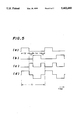
- FIG. 5 is a time chart for explaining the embodiment shown in FIG. 4.
- FIGS. 6 and 7 are time charts for explaining the effects of the present invention in comparison with the conventional call signal generating circuit.
- the call signal generating circuit shown in FIG. 3 includes a transformer 1, a transistor 2, a rectifying circuit 3, transistors 4 and 5, a capacitor 6, a resistor 7, a switching circuit 8, a control circuit 9, and output terminals 10 which are connected 5 as shown.
- the transistor 2 is connected between the primary winding of the transformer 1 and the D.C. power source (not shown), and this transistor 2 is turned ON/OFF at a frequency which is high compared to the frequency of the call signal which is generated by the call signal generating circuit.
- the rectifying circuit 3 rectifies the voltages induced at the secondary windings of the transformer 1 into positive and negative polarity voltages.
- the transistors 4 and 5 are alternately turned ON/OFF depending on the period of the call signal so as to respectively output the positive and negative polarity voltages from the rectifying circuit 3.
- the transistors 4 and 5 are controlled so that there exist quiescent times in which both the transistors 4 and 5 are turned OFF simultaneously.
- the positive and negative polarity voltages from the transistors 4 and 5 are applied to the capacitor 6.
- the switching circuit 8 is turned ON during the quiescent time in which both the transistors 4 and 5 are OFF simultaneously. When the switching circuit 8 is ON, the charge in the capacitor 6 is discharged via the resistor 7.
- the control circuit 9 controls the transistors 2, 4 and 5, and the switching circuit 8.
- the call signal is output via the output terminal 10.
- the voltages are induced 5 at the secondary windings of the transformer 1 by turning the transistor 2 at a frequency higher than the frequency of the call signal.
- the voltages induced at the secondary windings of the transformer 1 are rectified into the positive and negative polarity voltages by the rectifying circuit 3, and the positive polarity voltage is output via the transistor 4 while the negative polarity voltage is output via the transistor 5. Accordingly, by alternately turning the transistors 4 and 5 ON/OFF, it is possible to output a 16 Hz call signal from the output terminals 10.
- the call signal generating circuit shown in FIG. 4 includes a transformer 11 having a primary winding 11a and secondary windings 11b and 11c, a transistor 12 connected to the primary winding 11a of the transformer 11, a capacitor 13, diodes 14 and 15, phototransistors 16 and 17, a capacitor 18, a control circuit 19, photodiodes 20 and 21, diodes 22 through 25, a resistor 26, a phototransistor 27, a photodiode 28, and output terminals 32 which are connected as shown.
- the control 5 circuit 19 includes inverters 29 and 30, and an AND circuit 31 which are connected as shown.
- the diodes 22 through 25, the phototransistor 27 and the photodiode 28 form a switching circuit 8 which corresponds to the aforementioned switching circuit 8 shown in FIG. 3.
- a unipolarity switching element such as the phototransistor 27.
- a photo coupler is formed by the phototransistor 16 and the photodiode 20, and another photo coupler is formed by the phototransistor 17 and the photodiode 21.
- a photo coupler is also formed by the phototransistor 27 and the photodiode 28. It is of course possible to use a normal transistor in place of each of these photo couplers.
- the control circuit 19 controls the transistor 12 so that the transistor 12 turns ON/OFF at a frequency on the order of several tens of kHz. In addition, the control circuit 19 alternately supplies a current to the photodiodes 20 and 21 with the quiescent time.
- This control circuit 19 includes the inverters 29 and 30, and the AND circuit 31.
- the control circuit 19 may be realized by logic circuits or a programs of a microprocessor, similarly as in the case of the conventional call signal generating circuit.
- the transistor 12 which is connected to the primary winding 11a of the transformer 11 is turned ON/OFF by the control circuit 19 at the frequency of several tens of kHz, and the voltages induced at the secondary windings 11b and 11c of the transformer 11 are respectively rectified into the positive and negative polarity voltages by the diodes 14 and 15.
- the positive and negative polarity voltages are respectively applied to the phototransistors 16 and 17.
- the phototransistors 16 and 17 turn ON/OFF responsive to the light from the corresponding photodiodes 20 and 21.
- the positive and negative polarity voltages are alternately output from the output terminals 32 with the quiescent time.
- the output of the AND circuit 31 is "0" and thus, the photodiode 28 does not emit light. Accordingly, the phototransistor 27 is OFF during this time, and no current flows to the resistor 26 during the time in which the positive or negative polarity voltage is output. Furthermore, during the quiescent time in which no current is supplied to the photodiodes 20 and 21, the output of the AND circuit 31 is "1" and thus the photodiode 28 emits light in response to the current which is received.
- the phototransistor 27 is turned 0N responsive to the light emitted from the photodiode 28, and the charge of the capacitor 18 is discharged by the resistor 26 during the quiescent time of the phototransistors 16 and 17 via the bridge-connected diodes 22 through 25 and the phototransistor 27. In other words, even in the low-load state, it is possible to make the falling edge (and the corresponding rising edge) of the call signal waveform sharp.
- FIG. 5 is a time chart for explaining the operation of the embodiment shown in FIG. 4.
- (a) shows the current supplied to the photodiode 20
- (b) shows the current supplied to the photodiode 21
- (c) shows the current supplied to the photodiode 28, and
- (d) shows the call signal output from the output terminals 32.
- T1 one period of the 16 Hz call signal
- the phototransistor 27 turns ON during the quiescent times T3 and T5 so as to discharge the charge of the capacitor 18.
- the call signal shown in FIG. 5 (d) having the sharp falling edge (and corresponding rising edge) is output from the output terminals 21.
- the circuit construction of the switching circuit 8 is not limited to that of the embodiment shown in FIG. 4.
- FIGS. 6 and 7 are time charts for explaining the effects of the present invention in comparison with the conventional call signal generating circuit.
- FIG. 6 shows the call signal waveform obtained by the conventional call signal generating circuit shown in FIG. 1.
- (a) shows the call signal waveform when no telephone set is connected to the call signal generating circuit
- (b) shows the call signal waveform when one telephone set is connected to the call signal generating circuit.
- the falling edge (and the corresponding rising edge) of the call signal waveform is gradual.
- FIG. 7 shows the call signal waveform obtained by the call signal generating circuit shown in FIG. 4.
- (a) shows the call signal waveform when no telephone set is connected to the call signal generating circuit
- (b) shows the call signal waveform when one telephone set is connected to the call signal generating circuit.
- the falling edge (and the corresponding rising edge) of the call signal waveform is sharp compared to the call signal waveform shown in FIG. 6.
Landscapes
- Engineering & Computer Science (AREA)
- Power Engineering (AREA)
- Signal Processing (AREA)
- Devices For Supply Of Signal Current (AREA)
Applications Claiming Priority (2)
| Application Number | Priority Date | Filing Date | Title |
|---|---|---|---|
| JP3-219918 | 1991-08-30 | ||
| JP3219918A JPH0563798A (ja) | 1991-08-30 | 1991-08-30 | 呼出信号発生回路 |
Publications (1)
| Publication Number | Publication Date |
|---|---|
| US5402480A true US5402480A (en) | 1995-03-28 |
Family
ID=16743066
Family Applications (1)
| Application Number | Title | Priority Date | Filing Date |
|---|---|---|---|
| US07/931,000 Expired - Fee Related US5402480A (en) | 1991-08-30 | 1992-08-17 | Call signal generating circuit |
Country Status (3)
| Country | Link |
|---|---|
| US (1) | US5402480A (fr) |
| JP (1) | JPH0563798A (fr) |
| CA (1) | CA2076323C (fr) |
Cited By (8)
| Publication number | Priority date | Publication date | Assignee | Title |
|---|---|---|---|---|
| US5490054A (en) * | 1994-10-05 | 1996-02-06 | Ferro Magnetics Corporation | Ringing generator and method for converting DC to AC having continuously adjustable amplitude |
| US5682748A (en) * | 1995-07-14 | 1997-11-04 | Thermotek, Inc. | Power control circuit for improved power application and temperature control of low voltage thermoelectric devices |
| US5742491A (en) * | 1995-08-09 | 1998-04-21 | Lucent Technologies Inc. | Power converter adaptively driven |
| US5768368A (en) * | 1995-05-12 | 1998-06-16 | Koenig; Roger L. | T1 channel bank control process and apparatus |
| US5790654A (en) * | 1996-08-05 | 1998-08-04 | Telogy Networks, Inc. | Digitally controlled ring signal generator |
| US6288919B1 (en) * | 1999-12-16 | 2001-09-11 | Chippower.Com, Inc. | Single stage AC/DC converter high frequency AC distribution systems |
| US20060013024A1 (en) * | 2004-05-05 | 2006-01-19 | Erno Temesi | Rectifier circuit having a power factor correction |
| US20120195081A1 (en) * | 2011-01-27 | 2012-08-02 | Lineage Power Corporation | System and method for increasing dc power system efficiency without requiring a large battery reserve |
Citations (9)
| Publication number | Priority date | Publication date | Assignee | Title |
|---|---|---|---|---|
| JPS56132889A (en) * | 1980-03-24 | 1981-10-17 | Nec Corp | Trunk circuit |
| US4436960A (en) * | 1982-01-11 | 1984-03-13 | Bell Telephone Laboratories, Incorporated | Telephone ringing signal generator |
| JPS61247153A (ja) * | 1985-04-25 | 1986-11-04 | Fujitsu Ltd | 呼出信号装置 |
| US4656659A (en) * | 1985-07-18 | 1987-04-07 | Itt Corporation | Programmable ring signal generator |
| US4703500A (en) * | 1985-10-28 | 1987-10-27 | Northern Telecom Limited | Power amplifier |
| JPS63308458A (ja) * | 1987-06-10 | 1988-12-15 | Nec Corp | 呼出し信号発生回路 |
| US4866585A (en) * | 1988-06-08 | 1989-09-12 | Das Pawan K | AC to DC solid state power supply using high frequency pulsed power switching |
| US5122760A (en) * | 1990-05-17 | 1992-06-16 | Nec Corporation | Detector for automatic gain control amplifier circuit |
| US5134355A (en) * | 1990-12-31 | 1992-07-28 | Texas Instruments Incorporated | Power factor correction control for switch-mode power converters |
-
1991
- 1991-08-30 JP JP3219918A patent/JPH0563798A/ja not_active Withdrawn
-
1992
- 1992-08-17 US US07/931,000 patent/US5402480A/en not_active Expired - Fee Related
- 1992-08-18 CA CA002076323A patent/CA2076323C/fr not_active Expired - Fee Related
Patent Citations (9)
| Publication number | Priority date | Publication date | Assignee | Title |
|---|---|---|---|---|
| JPS56132889A (en) * | 1980-03-24 | 1981-10-17 | Nec Corp | Trunk circuit |
| US4436960A (en) * | 1982-01-11 | 1984-03-13 | Bell Telephone Laboratories, Incorporated | Telephone ringing signal generator |
| JPS61247153A (ja) * | 1985-04-25 | 1986-11-04 | Fujitsu Ltd | 呼出信号装置 |
| US4656659A (en) * | 1985-07-18 | 1987-04-07 | Itt Corporation | Programmable ring signal generator |
| US4703500A (en) * | 1985-10-28 | 1987-10-27 | Northern Telecom Limited | Power amplifier |
| JPS63308458A (ja) * | 1987-06-10 | 1988-12-15 | Nec Corp | 呼出し信号発生回路 |
| US4866585A (en) * | 1988-06-08 | 1989-09-12 | Das Pawan K | AC to DC solid state power supply using high frequency pulsed power switching |
| US5122760A (en) * | 1990-05-17 | 1992-06-16 | Nec Corporation | Detector for automatic gain control amplifier circuit |
| US5134355A (en) * | 1990-12-31 | 1992-07-28 | Texas Instruments Incorporated | Power factor correction control for switch-mode power converters |
Cited By (10)
| Publication number | Priority date | Publication date | Assignee | Title |
|---|---|---|---|---|
| US5490054A (en) * | 1994-10-05 | 1996-02-06 | Ferro Magnetics Corporation | Ringing generator and method for converting DC to AC having continuously adjustable amplitude |
| US5768368A (en) * | 1995-05-12 | 1998-06-16 | Koenig; Roger L. | T1 channel bank control process and apparatus |
| US5682748A (en) * | 1995-07-14 | 1997-11-04 | Thermotek, Inc. | Power control circuit for improved power application and temperature control of low voltage thermoelectric devices |
| US5742491A (en) * | 1995-08-09 | 1998-04-21 | Lucent Technologies Inc. | Power converter adaptively driven |
| USRE37221E1 (en) * | 1995-08-09 | 2001-06-12 | Lucent Technologies Inc. | Power converter adaptively driven |
| US5790654A (en) * | 1996-08-05 | 1998-08-04 | Telogy Networks, Inc. | Digitally controlled ring signal generator |
| US6288919B1 (en) * | 1999-12-16 | 2001-09-11 | Chippower.Com, Inc. | Single stage AC/DC converter high frequency AC distribution systems |
| US20060013024A1 (en) * | 2004-05-05 | 2006-01-19 | Erno Temesi | Rectifier circuit having a power factor correction |
| US20120195081A1 (en) * | 2011-01-27 | 2012-08-02 | Lineage Power Corporation | System and method for increasing dc power system efficiency without requiring a large battery reserve |
| US8743566B2 (en) * | 2011-01-27 | 2014-06-03 | General Electric Company | System and method for increasing DC power system efficiency without requiring a large battery reserve |
Also Published As
| Publication number | Publication date |
|---|---|
| JPH0563798A (ja) | 1993-03-12 |
| CA2076323C (fr) | 1996-08-13 |
| CA2076323A1 (fr) | 1993-03-01 |
Similar Documents
| Publication | Publication Date | Title |
|---|---|---|
| US6028776A (en) | Power factor correction converter | |
| US3737756A (en) | Converter circuit with balanced parallel switching paths | |
| US6362577B1 (en) | Discharge lamp lighting circuit | |
| US5034873A (en) | Circuit configuration for a fixed-frequency blocking oscillator converter switching power supply | |
| JPH02114861A (ja) | 断続調整型電源回路 | |
| CA2076323C (fr) | Circuit generateur de signaux d'appel | |
| JPH11122926A (ja) | 自励発振型スイッチング電源装置 | |
| US4223378A (en) | Switching regulator | |
| KR950035023A (ko) | 인버터의 전력 제어 회로 | |
| JP2934166B2 (ja) | 点灯装置 | |
| JPS60128867A (ja) | 直流一直流変換器 | |
| JP3327331B2 (ja) | スイッチング電源装置 | |
| JPH0315269A (ja) | 多出力スイッチング電源装置の起動回路 | |
| KR19980044509A (ko) | 고전압 발생회로 | |
| JP2964839B2 (ja) | 電力変換装置 | |
| JPH076892A (ja) | 調光用放電灯点灯装置 | |
| KR0140018Y1 (ko) | 배터리 충전회로 | |
| SU1704251A1 (ru) | Преобразователь переменного напр жени | |
| JP2676982B2 (ja) | Dc―dcコンバータ | |
| EP0706257A2 (fr) | Circuit d'alimentation à découpage | |
| JP2527920Y2 (ja) | 高圧電源回路 | |
| JPS64916B2 (fr) | ||
| JPH0345985B2 (fr) | ||
| JPS6151510B2 (fr) | ||
| JPH0245434B2 (ja) | Suitsuchingudengenkairo |
Legal Events
| Date | Code | Title | Description |
|---|---|---|---|
| AS | Assignment |
Owner name: FUJITSU LIMITED, JAPAN Free format text: ASSIGNMENT OF ASSIGNORS INTEREST.;ASSIGNOR:HIRAHARA, MINORU;REEL/FRAME:006237/0094 Effective date: 19920807 |
|
| FEPP | Fee payment procedure |
Free format text: PAYOR NUMBER ASSIGNED (ORIGINAL EVENT CODE: ASPN); ENTITY STATUS OF PATENT OWNER: LARGE ENTITY |
|
| FPAY | Fee payment |
Year of fee payment: 4 |
|
| FPAY | Fee payment |
Year of fee payment: 8 |
|
| REMI | Maintenance fee reminder mailed | ||
| LAPS | Lapse for failure to pay maintenance fees | ||
| STCH | Information on status: patent discontinuation |
Free format text: PATENT EXPIRED DUE TO NONPAYMENT OF MAINTENANCE FEES UNDER 37 CFR 1.362 |
|
| FP | Lapsed due to failure to pay maintenance fee |
Effective date: 20070328 |