WO2014057748A1 - Iii族窒化物複合基板およびその製造方法、ならびにiii族窒化物半導体デバイスの製造方法 - Google Patents
Iii族窒化物複合基板およびその製造方法、ならびにiii族窒化物半導体デバイスの製造方法 Download PDFInfo
- Publication number
- WO2014057748A1 WO2014057748A1 PCT/JP2013/073805 JP2013073805W WO2014057748A1 WO 2014057748 A1 WO2014057748 A1 WO 2014057748A1 JP 2013073805 W JP2013073805 W JP 2013073805W WO 2014057748 A1 WO2014057748 A1 WO 2014057748A1
- Authority
- WO
- WIPO (PCT)
- Prior art keywords
- group iii
- iii nitride
- substrate
- nitride film
- film
- Prior art date
- Legal status (The legal status is an assumption and is not a legal conclusion. Google has not performed a legal analysis and makes no representation as to the accuracy of the status listed.)
- Ceased
Links
Images


Classifications
-
- H—ELECTRICITY
- H10—SEMICONDUCTOR DEVICES; ELECTRIC SOLID-STATE DEVICES NOT OTHERWISE PROVIDED FOR
- H10P—GENERIC PROCESSES OR APPARATUS FOR THE MANUFACTURE OR TREATMENT OF DEVICES COVERED BY CLASS H10
- H10P14/00—Formation of materials, e.g. in the shape of layers or pillars
- H10P14/20—Formation of materials, e.g. in the shape of layers or pillars of semiconductor materials
- H10P14/32—Formation of materials, e.g. in the shape of layers or pillars of semiconductor materials characterised by intermediate layers between substrates and deposited layers
- H10P14/3242—Structure
- H10P14/3256—Microstructure
-
- H—ELECTRICITY
- H10—SEMICONDUCTOR DEVICES; ELECTRIC SOLID-STATE DEVICES NOT OTHERWISE PROVIDED FOR
- H10P—GENERIC PROCESSES OR APPARATUS FOR THE MANUFACTURE OR TREATMENT OF DEVICES COVERED BY CLASS H10
- H10P90/00—Preparation of wafers not covered by a single main group of this subclass, e.g. wafer reinforcement
- H10P90/19—Preparing inhomogeneous wafers
- H10P90/1904—Preparing vertically inhomogeneous wafers
- H10P90/1906—Preparing SOI wafers
- H10P90/1914—Preparing SOI wafers using bonding
- H10P90/1916—Preparing SOI wafers using bonding with separation or delamination along an ion implanted layer, e.g. Smart-cut
-
- B—PERFORMING OPERATIONS; TRANSPORTING
- B32—LAYERED PRODUCTS
- B32B—LAYERED PRODUCTS, i.e. PRODUCTS BUILT-UP OF STRATA OF FLAT OR NON-FLAT, e.g. CELLULAR OR HONEYCOMB, FORM
- B32B7/00—Layered products characterised by the relation between layers; Layered products characterised by the relative orientation of features between layers, or by the relative values of a measurable parameter between layers, i.e. products comprising layers having different physical, chemical or physicochemical properties; Layered products characterised by the interconnection of layers
- B32B7/04—Interconnection of layers
-
- H—ELECTRICITY
- H10—SEMICONDUCTOR DEVICES; ELECTRIC SOLID-STATE DEVICES NOT OTHERWISE PROVIDED FOR
- H10P—GENERIC PROCESSES OR APPARATUS FOR THE MANUFACTURE OR TREATMENT OF DEVICES COVERED BY CLASS H10
- H10P14/00—Formation of materials, e.g. in the shape of layers or pillars
- H10P14/20—Formation of materials, e.g. in the shape of layers or pillars of semiconductor materials
- H10P14/29—Formation of materials, e.g. in the shape of layers or pillars of semiconductor materials characterised by the substrates
- H10P14/2901—Materials
- H10P14/2907—Materials being Group IIIA-VA materials
- H10P14/2908—Nitrides
-
- H—ELECTRICITY
- H10—SEMICONDUCTOR DEVICES; ELECTRIC SOLID-STATE DEVICES NOT OTHERWISE PROVIDED FOR
- H10P—GENERIC PROCESSES OR APPARATUS FOR THE MANUFACTURE OR TREATMENT OF DEVICES COVERED BY CLASS H10
- H10P14/00—Formation of materials, e.g. in the shape of layers or pillars
- H10P14/20—Formation of materials, e.g. in the shape of layers or pillars of semiconductor materials
- H10P14/29—Formation of materials, e.g. in the shape of layers or pillars of semiconductor materials characterised by the substrates
- H10P14/2901—Materials
- H10P14/2921—Materials being crystalline insulating materials
-
- H—ELECTRICITY
- H10—SEMICONDUCTOR DEVICES; ELECTRIC SOLID-STATE DEVICES NOT OTHERWISE PROVIDED FOR
- H10P—GENERIC PROCESSES OR APPARATUS FOR THE MANUFACTURE OR TREATMENT OF DEVICES COVERED BY CLASS H10
- H10P14/00—Formation of materials, e.g. in the shape of layers or pillars
- H10P14/20—Formation of materials, e.g. in the shape of layers or pillars of semiconductor materials
- H10P14/29—Formation of materials, e.g. in the shape of layers or pillars of semiconductor materials characterised by the substrates
- H10P14/2901—Materials
- H10P14/2922—Materials being non-crystalline insulating materials, e.g. glass or polymers
-
- H—ELECTRICITY
- H10—SEMICONDUCTOR DEVICES; ELECTRIC SOLID-STATE DEVICES NOT OTHERWISE PROVIDED FOR
- H10P—GENERIC PROCESSES OR APPARATUS FOR THE MANUFACTURE OR TREATMENT OF DEVICES COVERED BY CLASS H10
- H10P14/00—Formation of materials, e.g. in the shape of layers or pillars
- H10P14/20—Formation of materials, e.g. in the shape of layers or pillars of semiconductor materials
- H10P14/29—Formation of materials, e.g. in the shape of layers or pillars of semiconductor materials characterised by the substrates
- H10P14/2924—Structures
- H10P14/2925—Surface structures
-
- H—ELECTRICITY
- H10—SEMICONDUCTOR DEVICES; ELECTRIC SOLID-STATE DEVICES NOT OTHERWISE PROVIDED FOR
- H10P—GENERIC PROCESSES OR APPARATUS FOR THE MANUFACTURE OR TREATMENT OF DEVICES COVERED BY CLASS H10
- H10P14/00—Formation of materials, e.g. in the shape of layers or pillars
- H10P14/20—Formation of materials, e.g. in the shape of layers or pillars of semiconductor materials
- H10P14/32—Formation of materials, e.g. in the shape of layers or pillars of semiconductor materials characterised by intermediate layers between substrates and deposited layers
-
- H—ELECTRICITY
- H10—SEMICONDUCTOR DEVICES; ELECTRIC SOLID-STATE DEVICES NOT OTHERWISE PROVIDED FOR
- H10P—GENERIC PROCESSES OR APPARATUS FOR THE MANUFACTURE OR TREATMENT OF DEVICES COVERED BY CLASS H10
- H10P14/00—Formation of materials, e.g. in the shape of layers or pillars
- H10P14/20—Formation of materials, e.g. in the shape of layers or pillars of semiconductor materials
- H10P14/34—Deposited materials, e.g. layers
- H10P14/3451—Structure
- H10P14/3452—Microstructure
-
- H—ELECTRICITY
- H10—SEMICONDUCTOR DEVICES; ELECTRIC SOLID-STATE DEVICES NOT OTHERWISE PROVIDED FOR
- H10P—GENERIC PROCESSES OR APPARATUS FOR THE MANUFACTURE OR TREATMENT OF DEVICES COVERED BY CLASS H10
- H10P90/00—Preparation of wafers not covered by a single main group of this subclass, e.g. wafer reinforcement
- H10P90/19—Preparing inhomogeneous wafers
- H10P90/1904—Preparing vertically inhomogeneous wafers
- H10P90/1906—Preparing SOI wafers
- H10P90/1914—Preparing SOI wafers using bonding
-
- H—ELECTRICITY
- H10—SEMICONDUCTOR DEVICES; ELECTRIC SOLID-STATE DEVICES NOT OTHERWISE PROVIDED FOR
- H10P—GENERIC PROCESSES OR APPARATUS FOR THE MANUFACTURE OR TREATMENT OF DEVICES COVERED BY CLASS H10
- H10P90/00—Preparation of wafers not covered by a single main group of this subclass, e.g. wafer reinforcement
- H10P90/19—Preparing inhomogeneous wafers
- H10P90/1904—Preparing vertically inhomogeneous wafers
- H10P90/1906—Preparing SOI wafers
- H10P90/1922—Preparing SOI wafers using silicon etch back techniques, e.g. BESOI or ELTRAN
-
- H—ELECTRICITY
- H10—SEMICONDUCTOR DEVICES; ELECTRIC SOLID-STATE DEVICES NOT OTHERWISE PROVIDED FOR
- H10W—GENERIC PACKAGES, INTERCONNECTIONS, CONNECTORS OR OTHER CONSTRUCTIONAL DETAILS OF DEVICES COVERED BY CLASS H10
- H10W10/00—Isolation regions in semiconductor bodies between components of integrated devices
- H10W10/10—Isolation regions comprising dielectric materials
- H10W10/181—Semiconductor-on-insulator [SOI] isolation regions, e.g. buried oxide regions of SOI wafers
-
- B—PERFORMING OPERATIONS; TRANSPORTING
- B32—LAYERED PRODUCTS
- B32B—LAYERED PRODUCTS, i.e. PRODUCTS BUILT-UP OF STRATA OF FLAT OR NON-FLAT, e.g. CELLULAR OR HONEYCOMB, FORM
- B32B2307/00—Properties of the layers or laminate
- B32B2307/20—Properties of the layers or laminate having particular electrical or magnetic properties, e.g. piezoelectric
-
- B—PERFORMING OPERATIONS; TRANSPORTING
- B32—LAYERED PRODUCTS
- B32B—LAYERED PRODUCTS, i.e. PRODUCTS BUILT-UP OF STRATA OF FLAT OR NON-FLAT, e.g. CELLULAR OR HONEYCOMB, FORM
- B32B7/00—Layered products characterised by the relation between layers; Layered products characterised by the relative orientation of features between layers, or by the relative values of a measurable parameter between layers, i.e. products comprising layers having different physical, chemical or physicochemical properties; Layered products characterised by the interconnection of layers
- B32B7/04—Interconnection of layers
- B32B7/06—Interconnection of layers permitting easy separation
-
- H—ELECTRICITY
- H10—SEMICONDUCTOR DEVICES; ELECTRIC SOLID-STATE DEVICES NOT OTHERWISE PROVIDED FOR
- H10D—INORGANIC ELECTRIC SEMICONDUCTOR DEVICES
- H10D62/00—Semiconductor bodies, or regions thereof, of devices having potential barriers
- H10D62/80—Semiconductor bodies, or regions thereof, of devices having potential barriers characterised by the materials
- H10D62/85—Semiconductor bodies, or regions thereof, of devices having potential barriers characterised by the materials being Group III-V materials, e.g. GaAs
- H10D62/8503—Nitride Group III-V materials, e.g. AlN or GaN
-
- H—ELECTRICITY
- H10—SEMICONDUCTOR DEVICES; ELECTRIC SOLID-STATE DEVICES NOT OTHERWISE PROVIDED FOR
- H10H—INORGANIC LIGHT-EMITTING SEMICONDUCTOR DEVICES HAVING POTENTIAL BARRIERS
- H10H20/00—Individual inorganic light-emitting semiconductor devices having potential barriers, e.g. light-emitting diodes [LED]
- H10H20/01—Manufacture or treatment
- H10H20/011—Manufacture or treatment of bodies, e.g. forming semiconductor layers
- H10H20/013—Manufacture or treatment of bodies, e.g. forming semiconductor layers having light-emitting regions comprising only Group III-V materials
- H10H20/0133—Manufacture or treatment of bodies, e.g. forming semiconductor layers having light-emitting regions comprising only Group III-V materials with a substrate not being Group III-V materials
- H10H20/01335—Manufacture or treatment of bodies, e.g. forming semiconductor layers having light-emitting regions comprising only Group III-V materials with a substrate not being Group III-V materials the light-emitting regions comprising nitride materials
-
- H—ELECTRICITY
- H10—SEMICONDUCTOR DEVICES; ELECTRIC SOLID-STATE DEVICES NOT OTHERWISE PROVIDED FOR
- H10H—INORGANIC LIGHT-EMITTING SEMICONDUCTOR DEVICES HAVING POTENTIAL BARRIERS
- H10H20/00—Individual inorganic light-emitting semiconductor devices having potential barriers, e.g. light-emitting diodes [LED]
- H10H20/01—Manufacture or treatment
- H10H20/011—Manufacture or treatment of bodies, e.g. forming semiconductor layers
- H10H20/018—Bonding of wafers
-
- H—ELECTRICITY
- H10—SEMICONDUCTOR DEVICES; ELECTRIC SOLID-STATE DEVICES NOT OTHERWISE PROVIDED FOR
- H10H—INORGANIC LIGHT-EMITTING SEMICONDUCTOR DEVICES HAVING POTENTIAL BARRIERS
- H10H20/00—Individual inorganic light-emitting semiconductor devices having potential barriers, e.g. light-emitting diodes [LED]
- H10H20/80—Constructional details
- H10H20/81—Bodies
- H10H20/815—Bodies having stress relaxation structures, e.g. buffer layers
-
- H—ELECTRICITY
- H10—SEMICONDUCTOR DEVICES; ELECTRIC SOLID-STATE DEVICES NOT OTHERWISE PROVIDED FOR
- H10H—INORGANIC LIGHT-EMITTING SEMICONDUCTOR DEVICES HAVING POTENTIAL BARRIERS
- H10H20/00—Individual inorganic light-emitting semiconductor devices having potential barriers, e.g. light-emitting diodes [LED]
- H10H20/80—Constructional details
- H10H20/81—Bodies
- H10H20/8215—Bodies characterised by crystalline imperfections, e.g. dislocations; characterised by the distribution of dopants, e.g. delta-doping
-
- H—ELECTRICITY
- H10—SEMICONDUCTOR DEVICES; ELECTRIC SOLID-STATE DEVICES NOT OTHERWISE PROVIDED FOR
- H10P—GENERIC PROCESSES OR APPARATUS FOR THE MANUFACTURE OR TREATMENT OF DEVICES COVERED BY CLASS H10
- H10P14/00—Formation of materials, e.g. in the shape of layers or pillars
- H10P14/20—Formation of materials, e.g. in the shape of layers or pillars of semiconductor materials
- H10P14/29—Formation of materials, e.g. in the shape of layers or pillars of semiconductor materials characterised by the substrates
-
- H—ELECTRICITY
- H10—SEMICONDUCTOR DEVICES; ELECTRIC SOLID-STATE DEVICES NOT OTHERWISE PROVIDED FOR
- H10P—GENERIC PROCESSES OR APPARATUS FOR THE MANUFACTURE OR TREATMENT OF DEVICES COVERED BY CLASS H10
- H10P14/00—Formation of materials, e.g. in the shape of layers or pillars
- H10P14/20—Formation of materials, e.g. in the shape of layers or pillars of semiconductor materials
- H10P14/32—Formation of materials, e.g. in the shape of layers or pillars of semiconductor materials characterised by intermediate layers between substrates and deposited layers
- H10P14/3202—Materials thereof
- H10P14/3214—Materials thereof being Group IIIA-VA semiconductors
- H10P14/3216—Nitrides
-
- H—ELECTRICITY
- H10—SEMICONDUCTOR DEVICES; ELECTRIC SOLID-STATE DEVICES NOT OTHERWISE PROVIDED FOR
- H10P—GENERIC PROCESSES OR APPARATUS FOR THE MANUFACTURE OR TREATMENT OF DEVICES COVERED BY CLASS H10
- H10P14/00—Formation of materials, e.g. in the shape of layers or pillars
- H10P14/20—Formation of materials, e.g. in the shape of layers or pillars of semiconductor materials
- H10P14/34—Deposited materials, e.g. layers
- H10P14/3402—Deposited materials, e.g. layers characterised by the chemical composition
- H10P14/3414—Deposited materials, e.g. layers characterised by the chemical composition being group IIIA-VIA materials
- H10P14/3416—Nitrides
-
- H—ELECTRICITY
- H10—SEMICONDUCTOR DEVICES; ELECTRIC SOLID-STATE DEVICES NOT OTHERWISE PROVIDED FOR
- H10P—GENERIC PROCESSES OR APPARATUS FOR THE MANUFACTURE OR TREATMENT OF DEVICES COVERED BY CLASS H10
- H10P14/00—Formation of materials, e.g. in the shape of layers or pillars
- H10P14/20—Formation of materials, e.g. in the shape of layers or pillars of semiconductor materials
- H10P14/36—Formation of materials, e.g. in the shape of layers or pillars of semiconductor materials characterised by treatments done before the formation of the materials
-
- H—ELECTRICITY
- H10—SEMICONDUCTOR DEVICES; ELECTRIC SOLID-STATE DEVICES NOT OTHERWISE PROVIDED FOR
- H10P—GENERIC PROCESSES OR APPARATUS FOR THE MANUFACTURE OR TREATMENT OF DEVICES COVERED BY CLASS H10
- H10P52/00—Grinding, lapping or polishing of wafers, substrates or parts of devices
- H10P52/40—Chemomechanical polishing [CMP]
- H10P52/402—Chemomechanical polishing [CMP] of semiconductor materials
-
- H—ELECTRICITY
- H10—SEMICONDUCTOR DEVICES; ELECTRIC SOLID-STATE DEVICES NOT OTHERWISE PROVIDED FOR
- H10P—GENERIC PROCESSES OR APPARATUS FOR THE MANUFACTURE OR TREATMENT OF DEVICES COVERED BY CLASS H10
- H10P72/00—Handling or holding of wafers, substrates or devices during manufacture or treatment thereof
- H10P72/70—Handling or holding of wafers, substrates or devices during manufacture or treatment thereof for supporting or gripping
- H10P72/74—Handling or holding of wafers, substrates or devices during manufacture or treatment thereof for supporting or gripping using temporarily an auxiliary support
- H10P72/7424—Handling or holding of wafers, substrates or devices during manufacture or treatment thereof for supporting or gripping using temporarily an auxiliary support used as a support during the manufacture of self-supporting substrates
-
- H—ELECTRICITY
- H10—SEMICONDUCTOR DEVICES; ELECTRIC SOLID-STATE DEVICES NOT OTHERWISE PROVIDED FOR
- H10P—GENERIC PROCESSES OR APPARATUS FOR THE MANUFACTURE OR TREATMENT OF DEVICES COVERED BY CLASS H10
- H10P72/00—Handling or holding of wafers, substrates or devices during manufacture or treatment thereof
- H10P72/70—Handling or holding of wafers, substrates or devices during manufacture or treatment thereof for supporting or gripping
- H10P72/74—Handling or holding of wafers, substrates or devices during manufacture or treatment thereof for supporting or gripping using temporarily an auxiliary support
- H10P72/744—Details of chemical or physical process used for separating the auxiliary support from a device or a wafer
-
- H—ELECTRICITY
- H10—SEMICONDUCTOR DEVICES; ELECTRIC SOLID-STATE DEVICES NOT OTHERWISE PROVIDED FOR
- H10P—GENERIC PROCESSES OR APPARATUS FOR THE MANUFACTURE OR TREATMENT OF DEVICES COVERED BY CLASS H10
- H10P90/00—Preparation of wafers not covered by a single main group of this subclass, e.g. wafer reinforcement
- H10P90/12—Preparing bulk and homogeneous wafers
- H10P90/129—Preparing bulk and homogeneous wafers by polishing
-
- Y—GENERAL TAGGING OF NEW TECHNOLOGICAL DEVELOPMENTS; GENERAL TAGGING OF CROSS-SECTIONAL TECHNOLOGIES SPANNING OVER SEVERAL SECTIONS OF THE IPC; TECHNICAL SUBJECTS COVERED BY FORMER USPC CROSS-REFERENCE ART COLLECTIONS [XRACs] AND DIGESTS
- Y10—TECHNICAL SUBJECTS COVERED BY FORMER USPC
- Y10T—TECHNICAL SUBJECTS COVERED BY FORMER US CLASSIFICATION
- Y10T428/00—Stock material or miscellaneous articles
- Y10T428/24—Structurally defined web or sheet [e.g., overall dimension, etc.]
- Y10T428/24273—Structurally defined web or sheet [e.g., overall dimension, etc.] including aperture
- Y10T428/24298—Noncircular aperture [e.g., slit, diamond, rectangular, etc.]
-
- Y—GENERAL TAGGING OF NEW TECHNOLOGICAL DEVELOPMENTS; GENERAL TAGGING OF CROSS-SECTIONAL TECHNOLOGIES SPANNING OVER SEVERAL SECTIONS OF THE IPC; TECHNICAL SUBJECTS COVERED BY FORMER USPC CROSS-REFERENCE ART COLLECTIONS [XRACs] AND DIGESTS
- Y10—TECHNICAL SUBJECTS COVERED BY FORMER USPC
- Y10T—TECHNICAL SUBJECTS COVERED BY FORMER US CLASSIFICATION
- Y10T428/00—Stock material or miscellaneous articles
- Y10T428/24—Structurally defined web or sheet [e.g., overall dimension, etc.]
- Y10T428/24273—Structurally defined web or sheet [e.g., overall dimension, etc.] including aperture
- Y10T428/24322—Composite web or sheet
- Y10T428/24331—Composite web or sheet including nonapertured component
-
- Y—GENERAL TAGGING OF NEW TECHNOLOGICAL DEVELOPMENTS; GENERAL TAGGING OF CROSS-SECTIONAL TECHNOLOGIES SPANNING OVER SEVERAL SECTIONS OF THE IPC; TECHNICAL SUBJECTS COVERED BY FORMER USPC CROSS-REFERENCE ART COLLECTIONS [XRACs] AND DIGESTS
- Y10—TECHNICAL SUBJECTS COVERED BY FORMER USPC
- Y10T—TECHNICAL SUBJECTS COVERED BY FORMER US CLASSIFICATION
- Y10T428/00—Stock material or miscellaneous articles
- Y10T428/24—Structurally defined web or sheet [e.g., overall dimension, etc.]
- Y10T428/24942—Structurally defined web or sheet [e.g., overall dimension, etc.] including components having same physical characteristic in differing degree
- Y10T428/2495—Thickness [relative or absolute]
- Y10T428/24967—Absolute thicknesses specified
- Y10T428/24975—No layer or component greater than 5 mils thick
-
- Y—GENERAL TAGGING OF NEW TECHNOLOGICAL DEVELOPMENTS; GENERAL TAGGING OF CROSS-SECTIONAL TECHNOLOGIES SPANNING OVER SEVERAL SECTIONS OF THE IPC; TECHNICAL SUBJECTS COVERED BY FORMER USPC CROSS-REFERENCE ART COLLECTIONS [XRACs] AND DIGESTS
- Y10—TECHNICAL SUBJECTS COVERED BY FORMER USPC
- Y10T—TECHNICAL SUBJECTS COVERED BY FORMER US CLASSIFICATION
- Y10T428/00—Stock material or miscellaneous articles
- Y10T428/26—Web or sheet containing structurally defined element or component, the element or component having a specified physical dimension
- Y10T428/263—Coating layer not in excess of 5 mils thick or equivalent
- Y10T428/264—Up to 3 mils
- Y10T428/265—1 mil or less
-
- Y—GENERAL TAGGING OF NEW TECHNOLOGICAL DEVELOPMENTS; GENERAL TAGGING OF CROSS-SECTIONAL TECHNOLOGIES SPANNING OVER SEVERAL SECTIONS OF THE IPC; TECHNICAL SUBJECTS COVERED BY FORMER USPC CROSS-REFERENCE ART COLLECTIONS [XRACs] AND DIGESTS
- Y10—TECHNICAL SUBJECTS COVERED BY FORMER USPC
- Y10T—TECHNICAL SUBJECTS COVERED BY FORMER US CLASSIFICATION
- Y10T428/00—Stock material or miscellaneous articles
- Y10T428/31—Surface property or characteristic of web, sheet or block
Definitions
- the present invention relates to a group III nitride composite substrate and a method for manufacturing the same, and a method for manufacturing a group III nitride semiconductor device using the group III nitride composite substrate.
- Group III nitride semiconductors such as GaN, AlN, and Al x Ga 1-x N (0 ⁇ x ⁇ 1) have excellent semiconductor characteristics and are therefore suitable as substrates for semiconductor devices. Since such a group III nitride semiconductor is expensive, from the viewpoint of reducing the manufacturing cost of the semiconductor device, as a substrate of the semiconductor device, a group III nitride semiconductor such as GaN or AlN is formed on a support substrate such as a silicon substrate. A semiconductor substrate on which a film is formed has been proposed.
- Patent Document 1 discloses a step of implanting ions in the vicinity of the surface of a first nitride semiconductor substrate made of GaN or AlN, and the surface of the first nitride semiconductor substrate. A step of superimposing the second substrate on the side, a step of heat-treating the two superimposed substrates, and a portion of the first nitride semiconductor substrate on the second layer with the ion-implanted layer as a boundary.
- a method for manufacturing a semiconductor substrate comprising a step of peeling off from a substrate.
- a semiconductor substrate obtained by the method for manufacturing a semiconductor substrate disclosed in Japanese Patent Application Laid-Open No. 2006-210660 has a thin film thickness of about 2 ⁇ m of a nitride semiconductor formed on a support substrate. There is a problem that the sheet resistance is increased, and there is a problem that a yield is lowered due to partial resistance increase due to damage caused by ion implantation.
- the present invention solves the above-described problems, and provides a group III nitride composite substrate having a low sheet resistance obtained with a high yield, a method for manufacturing the same, and a group III nitride semiconductor device using the group III nitride composite substrate It aims to provide a method.
- the group III nitride composite substrate includes a group III nitride film and a support substrate formed of a material having a chemical composition different from that of the group III nitride film.
- the group III nitride film is bonded to the support substrate in either a direct or indirect form.
- the thickness of the group III nitride film is 10 ⁇ m or more, and the sheet resistance on the main surface on the group III nitride film side is 200 ⁇ / sq (ohms per square) or less.
- the thickness of the group III nitride film is 10 ⁇ m or more, the sheet resistance on the main surface on the group III nitride film side can be lowered to 200 ⁇ / sq or less, and a high yield can be achieved.
- a group III nitride semiconductor device can be manufactured.
- the area of the bonding region between the group III nitride film and the support substrate is 70% or more of the area of the main surface, and the non-group between the group III nitride film and the support substrate
- the joining region includes at least one non-joining partial region, and the non-joining partial region can be a small non-joining partial region having a maximum diameter of less than 20 mm.
- the area of the junction region is as large as 70% or more of the area of the main surface, and the maximum diameter of the non-joint partial region constituting the non-joint region is small and less than 20 mm.
- a physical semiconductor device can be manufactured.
- the non-joining region between the group III nitride film and the support substrate includes at least one non-joining partial region, and the non-joining partial region is in contact with the outer periphery of the main surface. There can be no inner non-bonded partial area.
- the non-joining partial region constituting the non-joining region is not in contact with the outer periphery of the main surface, so that the group III nitride semiconductor device can be manufactured with a high yield.
- the group III nitride film has a main surface through hole, and the area of the main surface through hole can be 10% or less of the area of the main surface.
- the area of the main surface through hole of the group III nitride film is 10% or less of the area of the main surface, so that a group III nitride semiconductor device can be manufactured with a high yield.
- the junction interface between the group III nitride film and the support substrate contains an impurity including a metal, and the impurity concentration may be 1 ⁇ 10 10 cm ⁇ 2 or more. it can.
- the concentration of impurities including a metal at the bonding interface is 1 ⁇ 10 10 cm ⁇ 2 or more. Therefore, the group III nitride semiconductor device can be manufactured with high bonding strength and high yield. it can.
- the thermal expansion coefficient of the group III nitride film can be made larger than 0.7 times and smaller than 1.4 times compared with the thermal expansion coefficient of the supporting substrate.
- Such a group III nitride composite substrate has a group III nitride film having a thermal expansion coefficient larger than 0.7 times and smaller than 1.4 times compared with the thermal expansion coefficient of the support substrate.
- the group III nitride semiconductor device can be manufactured with a high yield by suppressing the occurrence of warpage and / or cracks.
- the fracture toughness of the supporting substrate and 1MNm -2/3 or more, the thickness of the supporting substrate may be equal to or larger than 50 [mu] m. Since the group III nitride composite substrate has high mechanical strength, a group III nitride semiconductor device can be manufactured with a high yield.
- the indirect form may be a form in which a bonding film is interposed between the group III nitride film and the support substrate.
- the group III nitride film and the support substrate are bonded together with a bonding film interposed between them, so that the bonding strength is high and the group III nitride is high in yield.
- Semiconductor devices can be manufactured.
- a method for producing a group III nitride composite substrate according to another aspect of the present invention is a method for producing a group III nitride composite substrate according to the above aspect, wherein the group III nitride film and the support substrate are directly and indirectly connected. And a step of reducing the thickness of at least one of the bonded group III nitride film and the supporting substrate.
- Such a method for producing a group III nitride composite substrate includes the above-described steps, whereby a group III nitride composite substrate having a high yield and a low sheet resistance can be produced.
- a method for producing a group III nitride semiconductor device is a method for producing a group III nitride semiconductor device using a group III nitride composite substrate according to the above aspect, comprising a group III nitride composite substrate And a step of growing at least one group III nitride layer on the main surface of the group III nitride composite substrate on the group III nitride film side.
- Such a group III nitride semiconductor device manufacturing method includes the above-described steps, whereby a group III nitride semiconductor device can be manufactured with a high yield.
- the present invention it is possible to provide a group III nitride composite substrate having a low sheet resistance obtained with a high yield, a method for manufacturing the same, and a method for manufacturing a group III nitride semiconductor device using the group III nitride composite substrate.
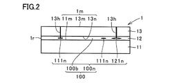
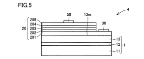
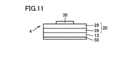
- a group III nitride composite substrate 1 is formed of a group III nitride film 13 and a material having a chemical composition different from that of group III nitride film 13. Supporting substrate 11.
- the group III nitride film 13 is bonded to the support substrate 11 in either a direct or indirect form.
- the thickness of the group III nitride film 13 is 10 ⁇ m or more.
- the sheet resistance on the main surface 13m on the group III nitride film 13 side is 200 ⁇ / sq or less.
- the sheet resistance on the main surface 13 m on the group III nitride film 13 side is as low as 200 ⁇ / sq or less.
- a group III nitride semiconductor device can be manufactured with a high yield. Details will be described below.
- the group III nitride composite substrate 1 of this embodiment includes a group III nitride film 13 and a support substrate 11 formed of a material having a chemical composition different from that of the group III nitride film 13.
- the group III nitride film 13 refers to a substrate formed of a semiconductor that is a compound of at least one group III element and nitrogen.
- the manufacturing method of the group III nitride film 13 is not particularly limited, and examples of the vapor phase method include an HVPE (hydride vapor phase growth) method and a sublimation method. Examples of the liquid phase method include a high nitrogen pressure solution method and a flux. Law.
- the group III nitride film 13 is preferably a crystal and more preferably a single crystal from the viewpoint of growing a group III nitride layer having high crystal quality on the group III nitride film 13.
- the group III nitride film 13 can be doped with a conductivity improving impurity in order to reduce the sheet resistance.
- conductivity improving impurities are not particularly limited, but O (oxygen) atoms, Si (silicon) atoms, and the like are preferable from the viewpoint of a high effect of improving conductivity.
- the support substrate 11 refers to a substrate that supports the group III nitride film 13 and is not particularly limited as long as it is formed of a material having a chemical composition different from that of the group III nitride film 13.
- oxide substrates sapphire substrates and other Al 2 O 3 substrates, mullite substrates and other Al 2 O 3 —SiO 2 based substrates, spinel substrates and other Al 2 O 3 —MgO based substrates, Al 2 O 3 And —SiO 2 —YSZ (yttria stabilized zirconia) based substrate.
- the metal substrate include a Mo substrate, a W substrate, and a Cu—W substrate.
- the group III nitride film 13 is a GaN film
- a substrate formed of AlN, which is a group III nitride having a chemical composition different from that of GaN may be used.
- the support substrate 11 may be crystalline or non-crystalline, and if it is a crystal, it may be a single crystal or a polycrystal.
- the group III nitride film 13 is bonded to the support substrate 11 in either a direct or indirect form.
- “bonded in a direct form” means that group III nitride film 13 and support substrate 11 are directly bonded without interposing another one therebetween. That means.
- the bonding interface 100 is a surface formed by the main surface 13n of the group III nitride film 13 and the main surface 11m of the support substrate 11 bonded to each other.
- “indirectly bonded” means that the group III nitride film 13 and the support substrate 11 are indirectly connected with another, for example, a bonding film 12 interposed therebetween. It means being joined.
- the bonding interface differs as follows depending on the bonding method.
- the bonding film 12 a is formed on the main surface 11 m of the support substrate 11 and the bonding film 12 b is formed on the main surface 13 n of the group III nitride film 13.
- the bonding interface Reference numeral 100 denotes a surface formed by the main surface 12am of the bonding film 12a and the main surface 12bn of the bonding film 12b inside the bonding film 12 bonded to each other.
- the bonding interface 100 is a surface formed by the main surface of the bonding film 12 and the main surface 13n of the group III nitride film 13 that are bonded to each other.
- the bonding interface 100 is a surface formed by the main surface of the bonding film 12 and the main surface 11m of the support substrate 11 that are bonded to each other.
- the bonding film 12 that can be included between the group III nitride film 13 and the support substrate 11 of the group III nitride composite substrate 1 of the present embodiment has a high bonding strength between the group III nitride film 13 and the support substrate 11.
- SiO 2 film, Si 3 N 4 film, AlN film, Al 2 O 3 film, TiO 2 film, TiN film, Ga 2 O 3 film, W film, Mo film, Au— Sn film etc. are mentioned.
- the thickness of the bonding film 12 is not particularly limited, but is preferably 0.05 ⁇ m or more, more preferably 0.1 ⁇ m or more from the viewpoint of increasing the bonding strength between the group III nitride film 13 and the support substrate 11. From the viewpoint of improving the in-plane uniformity and flatness of the bonding film 12, the thickness is preferably 5 ⁇ m or less, more preferably 2 ⁇ m or less.
- the thickness of the group III nitride film 13 needs to be 10 ⁇ m or more from the viewpoint of reducing the sheet resistance on the main surface 13m on the group III nitride film 13 side. 50 ⁇ m or more is preferable, and 100 ⁇ m or more is more preferable. Further, from the viewpoint of reducing the cost of the group III nitride composite substrate 1, the thickness of the group III nitride film 13 is preferably 500 ⁇ m or less, and more preferably 250 ⁇ m or less.
- the group III nitride composite substrate 1 of the present embodiment has the device characteristics of a group III nitride semiconductor device obtained by reducing the sheet resistance of the group III nitride composite substrate 1 (for example, the light emission efficiency of the light emitting device). From the viewpoint of increasing, the sheet resistance on the main surface 13m on the group III nitride film 13 needs to be 200 ⁇ / sq (ohms per square) or less, preferably 50 ⁇ / sq or less, and more preferably 10 ⁇ / sq or less.
- a group III nitride film 13 is bonded to the support substrate 11 at the bonding interface 100 described above. Also in the group III nitride composite substrate 1 of the present embodiment, the support substrate 11, the group III nitride film 13, and the bonding films 12, 12a, and 12b are similar to the group III nitride composite substrate manufactured by the ion implantation method.
- the surface roughness of the main surface, the main surface through-hole 13h of the group III nitride film 13 and the non-uniformity of bonding are present. Therefore, also in the group III nitride composite substrate 1 of the present embodiment, at the bonding interface 100, the bonding region 100b in which the group III nitride film 13 and the support substrate 11 are bonded either directly or indirectly. And a non-bonded region 100n where the group III nitride film 13 and the support substrate 11 are not bonded directly or indirectly.
- the presence, position, size, and area of the bonding region 100b and the non-bonding region 100n at the bonding interface 100 of the group III nitride composite substrate 1 of the present embodiment are determined using an ultrasonic microscope, a defect evaluation apparatus, or the like. Can be measured.
- the non-bonding region 100n in the bonding interface 100 of the group III nitride composite substrate 1 of the present embodiment includes at least one non-bonding partial region 111n, 112n, 121n, 122n.
- the non-junction partial regions 111n, 112n, 121n, and 122n have an indefinite shape but are substantially circular or elliptical, and therefore the size is evaluated based on the maximum diameter (maximum diameter). From the viewpoint of size, the non-joint partial regions 111n, 112n, 121n, and 122n are small non-joint partial regions 111n, 112n having a maximum diameter of less than 20 mm and large non-joint portions having a maximum diameter of 20 mm or more.
- the regions 121n and 122n can be classified.
- the non-joint partial regions 111n, 112n, 121n, and 122n are the inner non-joint partial regions 111n and 121n that are not in contact with the outer periphery 1r of the main surface 1m, and the regions are the main, from the viewpoint of the existence position. It can be classified into outer non-joined partial regions 112n and 122n in contact with the outer periphery 1r of the surface 1m.
- the group III nitride composite substrate 1 of the present embodiment has an area of the junction region 100b between the group III nitride film 13 and the support substrate 11 of 1 m on the main surface.
- the area is preferably 70% or more, more preferably 85% or more.
- the group III nitride film 13 and the support substrate are manufactured in the process of manufacturing the group III nitride semiconductor device. 11 is easily separated, and it is difficult to increase the yield of the group III nitride semiconductor device.
- the non-joint partial region is a small non-joint partial region 111n, 112n whose maximum diameter is less than 20 mm. It is preferable that That is, in FIG. 3, the non-joining partial regions are preferably small non-joining partial regions 111n and 112n.
- the group III nitride composite substrate 1 of the present embodiment has a non-bonded partial region that is not in contact with the outer periphery 1r of the main surface 1m.
- the partial regions 111n and 121n are preferable. That is, in FIG. 3, it is preferable that the non-joining partial regions are inner non-joining partial regions 111n and 121n.
- the group III nitride composite substrate 1 including the outer non-junction partial regions 112n and 122n is a group III nitride semiconductor device in the process of manufacturing the group III nitride composite substrate 1 and using the group III nitride composite substrate 1 During the manufacturing process, contaminants enter the bonding interface 100, and it is difficult to clean and remove the contaminants. Therefore, it is difficult to increase the yield of the group III nitride semiconductor device. Further, the group III nitride composite substrate 1 including the outer non-bonded partial regions 112n and 122n is being processed in the process of reducing the thickness of at least one of the group III nitride film 13 and the support substrate 11 bonded together. Therefore, it is difficult to increase the yield of the group III nitride semiconductor device.
- the non-joint partial region is more preferably a small and inner non-joint partial region 111n from the viewpoint of manufacturing a group III nitride semiconductor device with a high yield. That is, in FIG. 3, it is more preferable that the non-joining partial regions are small and inner non-joining partial regions 111n.
- group III nitride composite substrate 1 of the present embodiment includes a main surface through hole of group III nitride film 13 from the viewpoint of manufacturing a group III nitride semiconductor device with a high yield.
- the area of 13h is preferably 10% or less, and more preferably 5% or less with respect to the areas of the main surfaces 1m and 13m.
- the main surface through-hole 13h refers to the main surface of the group III nitride film 13 that is directly or indirectly bonded to the support substrate 11 and another surface (specifically, another main surface and A hole penetrating between the side surfaces.
- a non-bonding region 100n is formed on the main surface through hole 13h and in the vicinity thereof. Further, in the step of manufacturing the group III nitride semiconductor device, when the group III nitride semiconductor device is cleaned, the cleaning agent enters the bonding interface via the main surface through hole 13h, so that the group III nitride is obtained. The bonding strength of the composite substrate 1 may decrease. If the area of main surface through-hole 13h is larger than 10% of the area of main surface 1m, the area of non-junction region 100n increases, and it becomes difficult to increase the yield of group III nitride semiconductor devices.
- the group III nitride composite substrate 1 of the present embodiment has a group III nitride film 13 from the viewpoint of manufacturing a group III nitride semiconductor device with a high yield by increasing the bonding strength.
- the concentration of impurities including a metal contained in the bonding interface 100 between the support substrate 11 and the support substrate 11 is preferably 1 ⁇ 10 10 cm ⁇ 2 or more, and more preferably 1.5 ⁇ 10 10 cm ⁇ 2 or more. .
- the impurities including metal are not particularly limited, but from the viewpoint of increasing the bonding strength, when the group III nitride composite substrate 1 includes an oxide film such as a SiO 2 film as the bonding film 12, Fe (iron), Ni Base metal oxides such as (nickel) which have a higher ionization tendency than H (hydrogen) and are easily oxidized are preferred.
- the group III nitride composite substrate 1 of the present embodiment has a high yield by suppressing the occurrence of warpage and / or cracks during the manufacture of a group III nitride semiconductor device.
- the thermal expansion coefficient of the group III nitride film 13 is preferably greater than 0.7 times and smaller than 1.4 times the thermal expansion coefficient of the support substrate 11. 0.75 times or more and 1.25 times or less is more preferable.
- the group III nitride composite substrate 1 of the present embodiment is provided with a support substrate from the viewpoint of suppressing the occurrence of warpage and / or cracks during the manufacture of a group III nitride semiconductor device.
- fracture toughness is preferably not 1MNm -2/3 or more, more preferably 1.5MNm -2/3 or more.
- the thickness of the support substrate is preferably 50 ⁇ m or more, more preferably 100 ⁇ m or more.
- the method for manufacturing group III nitride composite substrate 1 according to another embodiment of the present invention is the method for manufacturing group III nitride composite substrate 1 according to the first embodiment. Then, the step of bonding the group III nitride film 13 and the support substrate 11 in a direct or indirect form (FIG. 4A), the group III nitride film 13 and the support substrate 11 And a step of reducing at least one thickness (FIG. 4B).
- the manufacturing method of the group III nitride composite substrate 1 of this embodiment can manufacture a group III nitride composite substrate having a high yield and a low sheet resistance by including the above steps.
- Step of bonding group III nitride film and supporting substrate With reference to FIGS. 1, 2, and 4, in the method of manufacturing group III nitride composite substrate 1 of this embodiment, first, group III nitride film 13 and support substrate 11 are directly and indirectly bonded. In any form, the process of bonding is included.
- the group III nitride film 13 and the support substrate 11 are bonded together in a direct form means that the group III nitride film 13 and the support substrate 11 are directly connected without interposing any other material therebetween. It means sticking together.
- bonding the group III nitride film 13 and the support substrate 11 in an indirect form means that the group III nitride film 13 and the support substrate 11 are sandwiched between them, for example, a bonding film 12. Indirect bonding.
- the method of bonding the group III nitride film 13 and the support substrate 11 is not particularly limited in any of the direct and indirect bonding modes, and after the bonded surfaces are washed and bonded as they are, 600 Direct bonding method in which bonding is performed by raising the temperature to about °C to 1200 °C, and the surface to be bonded in a low temperature atmosphere of room temperature (for example, 25 °C) to about 400 °C after cleaning the bonded surfaces and activating with plasma or ions Activated bonding method, after the bonded surface is cleaned with a chemical solution and pure water, and then the high pressure bonding method in which a high pressure of about 0.1 MPa to 10 MPa is applied and after the bonded surface is cleaned with a chemical solution and pure water A high vacuum bonding method in which bonding is performed in a high vacuum atmosphere of about 10 ⁇ 6 Pa to 10 ⁇ 3 Pa is suitable.
- the bonding strength can be further increased by raising the temperature to about 600 ° C. to 1200 ° C. after the bonding.
- the effect of increasing the bonding strength by raising the temperature to about 600 ° C. to 1200 ° C. after the bonding is large.
- the group III nitride film 13 and the support substrate 11 can be bonded in any of the direct and indirect forms as described above, but from the viewpoint of increasing the bonding strength, FIG. As shown in A), it is preferable that the group III nitride film 13 and the support substrate 11 are bonded indirectly with a bonding film 12 interposed therebetween. Details will be described below.
- the step of indirectly bonding the group III nitride film 13 and the support substrate 11 with the bonding film 12 interposed therebetween is performed on the main surface 11m of the support substrate 11.
- a sub-process for forming 12a (FIG. 4A1), a sub-process for forming the bonding film 12b on the main surface 13n of the group III nitride film 13 (FIG. 4A2), and a main surface of the support substrate 11.
- the bonding film 12a and the bonding film 12b bonded together are integrated by bonding to form the bonding film 12, and the support substrate 11 and the group III nitride film 13 interpose the bonding film 12. Let them join.
- the surface roughness of the main surface of the support substrate 11, the group III nitride film 13, and the bonding films 12, 12a, 12b, the group III nitride film 13 are bonded either directly or indirectly at the bonding interface 100 due to the presence of the main surface through-hole 13h and the non-uniformity of the bonding.
- Region 100b, and non-bonded region 100n where group III nitride film 13 and support substrate 11 are not directly or indirectly bonded are formed.
- the bonding region 100b and the non-bonding region 100n are as described above.
- the method for forming the bonding films 12a and 12b is not particularly limited, but from the viewpoint of suppressing the film formation cost, a sputtering method, a vapor deposition method, a CVD (chemical vapor deposition) method, or the like is preferably performed. Further, the method for bonding the supporting substrate 11 and the group III nitride film 13 by bonding the bonding film 12a and the bonding film 12b is not particularly limited. As described above, the direct bonding method and the surface activation are performed. A bonding method, a high pressure bonding method, a high vacuum bonding method, or the like is preferable.
- Step of reducing the thickness of at least one of the group III nitride film and the supporting substrate Referring to FIG. 4B, in the manufacturing method of group III nitride composite substrate 1 of the present embodiment, the thickness of at least one of group III nitride film 13 and support substrate 11 bonded together is then determined. And making it smaller.
- the method of reducing the thickness of at least one of the group III nitride film 13 and the support substrate 11 is not particularly limited, and is a method of cutting the substrate to be reduced in thickness parallel to the main surface, Examples thereof include a method for grinding and / or polishing a surface, a method for etching a main surface, and a method using a laser.
- the method using a laser is a method of irradiating a laser beam such that the focal point of the laser beam is located at a predetermined depth from the main surface of the substrate.
- the substrate can be separated in the region by changing the chemical composition of the region where the laser beam is focused at a predetermined depth from the main surface of the substrate.
- a femtosecond laser from the viewpoint of changing the chemical composition of a region at a predetermined depth from the main surface of the substrate and not changing the chemical composition of a region other than the above region, a femtosecond laser, A second laser is preferably used.
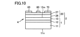
- the manufacturing method of group III nitride semiconductor device 4 which is still another embodiment of the present invention includes a step of preparing group III nitride composite substrate 1, Growing at least one group III nitride layer 20 on the main surface 13m on the group III nitride film 13 side.
- the manufacturing method of the group III nitride semiconductor device 4 of this embodiment can manufacture a group III nitride semiconductor device with a high yield by providing said process.
- the manufacturing method of the group III nitride semiconductor device 4 of the present embodiment first includes a step of preparing the group III nitride composite substrate 1.
- the step of preparing the group III nitride composite substrate 1 is the same as the step in the method for manufacturing the group III nitride composite substrate 1 of the second embodiment.
- Step of growing group III nitride layer In the method of manufacturing the group III nitride semiconductor device 4 of the present embodiment, at least one group III nitride layer 20 is then formed on the main surface 13m of the group III nitride composite substrate 1 on the group III nitride film 13 side. Including a growth step.
- the method for growing the group III nitride layer 20 is not particularly limited, but from the viewpoint of growing the group III nitride layer 20 with high crystal quality, as a vapor phase method, an MOCVD (metal organic chemical vapor deposition) method, An MBE (molecular beam growth) method, an HVPE (hydride vapor phase epitaxy) method, a sublimation method, and the like are preferable.
- a vapor phase method an MOCVD (metal organic chemical vapor deposition) method, An MBE (molecular beam growth) method, an HVPE (hydride vapor phase epitaxy) method, a sublimation method, and the like are preferable.
- a liquid phase method a high nitrogen pressure solution method, a flux method, and the like are preferable.
- the structure of the group III nitride layer 20 to be grown differs depending on the type and function of the group III nitride semiconductor device.
- the group III nitride semiconductor device 4 is a light emitting device
- the first conductivity type GaN layer is formed as the group III nitride layer 20 on the main surface 13m of the group III nitride composite substrate 1 on the group III nitride film 13 side.
- first conductivity type Al s Ga 1-s N layer 202 (where s is 0 ⁇ s ⁇ 1)
- light emitting layer 203
- second conductivity type Al t Ga 1-t N layer 204 (where t 0 ⁇ t ⁇ 1)
- the second conductivity type GaN layer 205 can be grown in this order.
- the manufacturing method of the group III nitride semiconductor device 4 of this embodiment can then include a step of forming electrodes (first electrode and second electrode).
- a part of each of the second conductivity type GaN layer 204, the light emitting layer 203, the first conductivity type Al s Ga 1-s N layer 202, and the first conductivity type GaN layer 201 is mesoscopic. By removing by etching, a part of the first conductivity type GaN layer 201 is exposed.
- the first electrode 31 can be formed on the exposed main surface of the first conductivity type GaN layer 201, and the second electrode can be formed on the exposed main surface of the second conductivity type GaN layer.
- the formation method of the first electrode 31 and the second electrode 32 is not particularly limited, and examples thereof include a CVD (chemical vapor deposition) method, a sputtering method, and a vapor deposition method.
- Reference invention I is a group III nitride composite substrate having a group III nitride film having a low cost, a large diameter, a large film thickness, a small film thickness distribution, and a high crystal quality, a method for manufacturing the same, and a laminated group III nitride composite substrate And a group III nitride semiconductor device and a method for manufacturing the same.
- Group III nitrides such as GaN are suitably used for semiconductor devices because they have excellent semiconductor properties.
- Japanese Patent Laid-Open No. 2009-126722 discloses a self-standing group III nitride substrate having a diameter of 25 mm or more and 160 mm or more and a thickness of 100 ⁇ m or more and 1000 ⁇ m or less as a semiconductor device substrate, as a specific example, a diameter of 100 mm and a thickness.
- a self-standing GaN substrate having a thickness of 400 ⁇ m is disclosed.
- Japanese Patent Application Laid-Open No. 2008-010766 discloses a heterogeneous substrate having a chemical composition different from that of GaN as a substrate for manufacturing a semiconductor device, and a GaN thin film having a thickness of 0.1 ⁇ m or more and 100 ⁇ m or less bonded to the heterogeneous substrate. And a GaN thin film bonded substrate having a diameter of 50.8 mm in which a sapphire substrate and a GaN thin film having a thickness of 0.1 ⁇ m or 100 ⁇ m are bonded as a specific example. .
- Japanese Unexamined Patent Application Publication No. 2010-182936 discloses a composite substrate including a support substrate, a nitride semiconductor layer, and a bonding layer provided between the support substrate and the nitride semiconductor layer as a semiconductor device substrate.
- a composite substrate is disclosed in which the thickness of a GaN layer bonded to a sapphire substrate and a GaN layer by a bonding layer formed by pressure bonding is 5 ⁇ m to 220 ⁇ m and the diameter is 50.8 mm.
- the GaN thin film bonded substrate disclosed in JP 2008-010766 A with a GaN thin film thickness of 0.1 ⁇ m is ion-implanted to form the GaN thin film.
- the thickness of the GaN thin film is preferably 10 ⁇ m or more.
- the thickness of the GaN thin film is increased, the depth of the ion implantation from the main surface is increased. There is a problem that the variation becomes large and the variation in the thickness of the GaN thin film of the obtained GaN thin film composite substrate becomes large.
- Each of the substrates has a diameter of about 50.8 mm, and there is a problem that the distribution in the main surface of the thickness of the GaN thin film or the GaN layer increases as the diameter increases.
- Reference invention I solves the above problems, and a group III nitride composite substrate having a group III nitride film having a low cost, a large diameter, a large film thickness, a small film thickness distribution, and a high crystal quality, and a method for manufacturing the same It is an object of the present invention to provide a laminated group III nitride composite substrate, a group III nitride semiconductor device, and a manufacturing method thereof.
- the reference invention I is a group III nitride composite substrate having a diameter of 75 mm or more obtained by bonding a supporting substrate and a group III nitride film having a thickness of 10 ⁇ m to 250 ⁇ m, the ratio s t / m t of the standard deviation s t of the thickness to the average value m t of the thickness of the nitride layer is 0.001 to 0.2, III-nitride films predetermined main surface of is the ratio s o / m o of the standard deviation s o of the absolute value of the off-angle with respect to the average value m o of the absolute value of the off angle of 0.005 to 0.6 with respect to the plane of the plane orientation, III-nitride composite It is a substrate.
- the warp on the main surface of the group III nitride composite substrate on the group III nitride film side is 50 ⁇ m or less, and the total thickness distribution of the group III nitride composite substrate ( It is also referred to as TTV.
- the ratio ⁇ III-N / ⁇ S of the thermal expansion coefficient of the III nitride film to the thermal expansion coefficient alpha S of the supporting substrate alpha III-N and 0.75 to 1.25, the thickness of the support substrate t the ratio t III-N / t S of thickness t III-N III nitride film to S may be 0.02 or more and 1 or less.
- impurity metal atoms in the main surface of the group III nitride film can be 3 ⁇ 10 12 atoms / cm 2 or less.
- the root mean square roughness of the main surface of the group III nitride film can be 3 nm or less.
- the root mean square roughness of the main surface of the support substrate can be 12 nm or less.
- the diameter of the group III nitride composite substrate can be 100 mm or more, and can be 125 mm or more and 300 mm or less.
- the main surface of the group III nitride film has an average value m III-N of the root mean square roughness of 0.1 nm to 2 nm, and a standard deviation s III-N of the root mean square roughness of 0. 4 nm or less
- the main surface of the support substrate can have an average value of root mean square roughness m S of 0.3 to 10 nm, and a standard deviation s S of root mean square roughness of 3 nm or less.
- the group III nitride composite substrate according to the above aspect and at least one group III nitride layer disposed on the group III nitride film of the group III nitride composite substrate And a laminated group III nitride composite substrate.
- the group III nitride film in the group III nitride composite substrate according to the above aspect and at least one group III nitride arranged on the group III nitride film
- a III-nitride semiconductor device comprising a layer.
- Reference invention I is a method for producing a group III nitride composite substrate according to the above aspect, according to still another aspect, wherein the diameter of the substrate is bonded to the support substrate and the group III nitride film donor substrate.
- a method for manufacturing a group III nitride composite substrate A method for manufacturing a group III nitride composite substrate.
- Reference invention I is a method for producing a group III nitride composite substrate according to the above aspect, according to still another aspect, wherein the diameter of the substrate is bonded to the support substrate and the group III nitride film donor substrate.
- a method for manufacturing a group III nitride composite substrate is a method for producing a group III nitride composite substrate according to the above aspect, according to still another aspect, wherein the diameter of the substrate is bonded to the support substrate and the group III nitride film donor substrate.
- a method of manufacturing a group III nitride semiconductor device includes a step of further bonding a device support substrate on the group III nitride layer, and a step of removing the support substrate from the group III nitride composite substrate. , May further be included.
- Group III nitride composite substrate Referring to FIG. 6, group III nitride composite substrate 1, which is a reference form of reference invention I, is bonded to support substrate 11 and group III nitride film 13 having a thickness of 10 ⁇ m to 250 ⁇ m.
- the ratio s t / m t of the standard deviation s t of the thickness to the average value m t of the thickness of the III nitride film 13 is 0.001 or more is 0.2 or less
- III group ratio s o of the standard deviation s o of the absolute value of the off-angle with respect to the average value m o of the absolute value of the off-angle with respect to a predetermined plane surface of the orientation of the principal surface 13m nitride film 13 / Mo is 0.005 or more and 0.6 or less.
- the group III nitride composite substrate 1 of this reference embodiment has a diameter of 75 mm or more, and the group III nitride film 13 bonded on the support substrate 11 has a thickness of 10 ⁇ m or more and 250 ⁇ m or less. average 0.2 below the ratio s t / m t of the standard deviation s t a thickness of 0.001 or more with respect to m t of the average of the absolute value of the off angle relative to the plane of the predetermined plane orientation of the main surface 13m by the ratio s o / m o of the standard deviation s o of the absolute value of the off angle with respect to the value m o is 0.005 to 0.6, on the III nitride film 13, the crystal quality in large diameter Since at least one high group III nitride layer can be grown, a group III nitride semiconductor device having high characteristics can be obtained with high yield.
- the bonding form of the support substrate 11 and the group III nitride film 13 is not particularly limited, but in order to increase the bonding strength by bonding, the bonding film 12 is formed. It is preferable to interpose.
- the diameter of the group III nitride composite substrate 1 is 75 mm or more, preferably 100 mm or more, more preferably 125 mm or more, and more preferably 150 mm or more from the viewpoint of increasing the number of chips of a semiconductor device from one composite substrate. preferable. Further, the diameter of the group III nitride composite substrate 1 is preferably 300 mm or less, and more preferably 200 mm or less, from the viewpoint of reducing the warpage of the composite substrate and increasing the yield of the semiconductor device.
- the warp of the group III nitride composite substrate 1 on the group III nitride film 13 side is preferably 50 ⁇ m or less, more preferably 30 ⁇ m or less, and even more preferably 20 ⁇ m or less from the viewpoint of increasing the yield of the semiconductor device to be formed.
- the warp of the group III nitride composite substrate 1 on the group III nitride film 13 side is the least square that minimizes the square of the distance to any point in the main surface 13 m of the group III nitride film 13.
- the TTV (referred to as Total Tickness Variation, which is one of the evaluation indices of flatness, also referred to as GBIR (Global Backside Ideal Range)) of the group III nitride composite substrate 1 is a viewpoint of increasing the yield of the semiconductor device to be formed. Therefore, 30 ⁇ m or less is preferable, 20 ⁇ m or less is more preferable, and 10 ⁇ m or less is more preferable.
- the TTV of the group III nitride composite substrate 1 is the group III nitride composite substrate 1 measured in the thickness direction with the main surface of the support substrate 11 which is the back surface of the group III nitride composite substrate 1 as a reference plane.
- the level difference of the main surface of the group III nitride film 13 which is the surface of the group III nitride composite substrate 1 in a state where the surface is flattened using the surface as a reference surface is the flatness of the optical interference type. It is measured by a measuring device, a laser displacement meter, or the like.
- the ratio ⁇ III-N / ⁇ S of the thermal expansion coefficient ⁇ III-N of the group III nitride film to the thermal expansion coefficient ⁇ S of the support substrate is determined on the group III nitride composite substrate 1 and its group III nitride film 13. From the viewpoint of reducing warpage and cracking of the group III nitride layer to be grown, 0.75 or more and 1.25 or less are preferable, 0.8 or more and 1.2 or less are more preferable, and 0.9 or more and 1.1 or less are further included. 0.95 or more and 1.05 or less are particularly preferable.
- the ratio t III-N / t S of the thickness t III-N of the group III nitride film to the thickness t S of the support substrate is determined on the group III nitride composite substrate 1 and the group III nitride film 13. From the viewpoint of reducing warpage and cracking of the group III nitride layer to be grown, 0.02 to 1 is preferable, 0.06 to 0.7 is more preferable, 0.15 to 0.5 is more preferable, 0.2 or more and 0.4 or less are particularly preferable.
- the support substrate 11 is not particularly limited as long as it can support the group III nitride film 13, but from the viewpoint of reducing the cost by reducing the amount of expensive group III nitride used, A different composition substrate having a different composition is preferable. Furthermore, as described above, the ratio ⁇ III-N / ⁇ S of the thermal expansion coefficient ⁇ III-N of the group III nitride film 13 to the thermal expansion coefficient ⁇ S of the support substrate 11 is 0.75 or more and 1.25 or less.
- the support substrate 11 is made of mullite (3Al 2 O 3 .2SiO 2 to 2Al 2 O 3 .SiO 2 ), mullite-YSZ (yttria stabilized zirconia), spinel (MgAl 2 O 4 ), Al A sintered body of 2 O 3 —SiO 2 composite oxide, and a substrate formed of a sintered body obtained by adding an oxide, carbonate or the like to these, a molybdenum (Mo) substrate, a tungsten (W) substrate, or the like is preferable. .
- the elements contained in the oxide and carbonate are Ca, Mg, Sr, Ba, Al, Sc, Y, Ce, Pr, Si, Ti, Zr, V, Nb, Ta, Cr, Mn, Fe, Preferred examples include Co, Ni, Cu, and Zn.
- the root mean square roughness (hereinafter also referred to as RMS) of main surface 11n of support substrate 11 in group III nitride composite substrate 1 grows on group III nitride film 13 of group III nitride composite substrate 1. From the viewpoint of improving the crystal quality of the group III nitride layer to be formed, 12 nm or less is preferable, 6 nm or less is more preferable, and 2 nm or less is more preferable.
- the RMS of the main surface 11n of the support substrate 11 is polished before the group III nitride film 13 is bonded, or the main surface that is not bonded is polished after the group III nitride film 13 is bonded. Can be adjusted.
- the RMS of the main surface 11n of the support substrate 11 calculates the reference plane from each point of the main surface 11n of the support substrate 11, and is the value of the average positive square root of the square of the distance to each point from the reference plane. It is measured with an AFM (Atomic Force Microscope), an optical interference type roughness meter, a stylus type roughness meter, or the like.
- AFM Acoustic Force Microscope
- the main surface 11n of the support substrate 11 preferably has an RMS average value m S of 0.3 nm to 10 nm and a RMS standard deviation s S of 3 nm or less.
- the RMS average value m S is set to 10 nm or less
- the RMS standard deviation s S is set to 3 nm or less. Since a high-quality group III nitride layer can be grown, a semiconductor device can be obtained with a high yield.
- advanced surface polishing is required, and the cost is greatly increased.
- the RMS average value m S of the main surface 11n of the support substrate 11 is more preferably 0.3 nm or more and 5 nm or less, and further preferably 0.3 nm or more and 2 nm or less. Further, the RMS standard deviation s S of the main surface 11n of the support substrate 11 is more preferably 2 nm or less, and further preferably 1 nm or less.
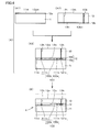
- the RMS average value m S and the standard deviation s S of the main surface 11n of the support substrate 11 are respectively calculated from the RMS measured at 13 measurement points on the main surface 11n of the support substrate 11 shown in FIG. Mean value and standard deviation.
- the 13 measurement points P on the main surface 11n of the support substrate 11 shown in FIG. 7 are one center point P C and 4 perpendicular to the center point P C regardless of the diameter of the support substrate 11. and four outer points P O in the direction on a and the outer edge to 5mm inside each other's middle four points and four outer points located in the middle of one of the center points P C and four outer points P O It is composed of eight intermediate points P M that are a combination of four positions.
- the standard deviation here means the positive square root of unbiased variance.
- Bonding film 12 is not particularly limited as long as it can bond the support substrate 11 and the III nitride film 13, is a high viewpoint bonding strength between the supporting substrate 11 and the III nitride film 13, SiO 2 A film, a Si 3 N 4 film, a TiO 2 film, a Ga 2 O 3 film, or the like is preferable.
- III-nitride film 13 is a film formed of a group III nitride, GaN film, In x Al y Ga 1- xy N film (0 ⁇ x, 0 ⁇ y , x + y ⁇ 1) such as AlN film Etc.
- the thickness of the group III nitride film 13 is 10 ⁇ m or more, preferably 30 ⁇ m or more, more preferably 50 ⁇ m or more, and further preferably 100 ⁇ m or more from the viewpoint of forming a high-performance group III nitride semiconductor device. Further, the thickness of the group III nitride film 13 is 250 ⁇ m or less, preferably 200 ⁇ m or less, preferably 170 ⁇ m or less, and more preferably 150 ⁇ m or less, from the viewpoint of reducing the amount of expensive group III nitride used.
- the ratio s t / m t of the standard deviation s t thickness average thickness for the m t of the III nitride film 13 is 0.001 to 0.2, 0.001 to 0.15 Is preferable, 0.002 or more and 0.1 or less are more preferable, and 0.01 or more and 0.05 or less are more preferable.
- the ratio s t / m t since the cutting and polishing to control the highly thickness is required, costs increase.
- the ratio s t / m t is larger than 0.2, since the uniformity of the film thickness is reduced, the characteristics of the resulting semiconductor device is reduced.
- the ratio s o / m o occurs in larger when group III nitride film 13 portion morphology of group III nitride layer is lowered onto the plane than 0.6, also in-plane distribution of the impurity incorporation increases Therefore, the yield of the obtained semiconductor device is reduced.
- the crystal structure of the group III nitride film 13 is preferably a wurtzite structure from the viewpoint of obtaining a semiconductor device with good characteristics.
- the above-mentioned predetermined plane orientation that is most approximate to the main surface 13m of the group III nitride film 13 is not limited as long as it is suitable for a desired semiconductor device, and is ⁇ 0001 ⁇ , ⁇ 10-10 ⁇ , ⁇ 11- 20 ⁇ , ⁇ 21-30 ⁇ , ⁇ 20-21 ⁇ , ⁇ 10-11 ⁇ , ⁇ 11-22 ⁇ , ⁇ 22-43 ⁇ , and plane orientations off at 15 ° or less from their respective plane orientations Good.
- the surface orientation of the back surface of each of these surface orientations and the surface orientation turned off at 15 ° or less from the surface orientation of the back surface may be used. That is, the main surface 13m of the group III nitride film 13 may be any of a polar surface, a nonpolar surface, and a semipolar surface. Further, the principal surface 13m of the group III nitride film 13 is preferably a ⁇ 0001 ⁇ surface and its back surface from the viewpoint of easily increasing the diameter, and a ⁇ 10-10 ⁇ surface from the viewpoint of suppressing the blue shift of the resulting light emitting device. , ⁇ 20-21 ⁇ surfaces and their back surfaces are preferred.
- the standard deviation s o Group III average thickness value m t of the nitride film 13 are the standard deviation m t of thickness, the average value m o of the off-angles, and the off angles, respectively, shown in FIG. 7 These are the average value and standard deviation calculated from the thicknesses and off-angles measured at 13 measurement points on the main surface 13m of group III nitride film 13. Measurement point P of 13 points on the major surface 13m of the III nitride film 13 shown in FIG.
- the center point P C Four outer points P O on four directions perpendicular to each other and 5 mm inside from the outer edge, four points located between one center point P C and four outer points P O and four outer points And eight intermediate points P M obtained by combining four points located in the middle of each other.
- the standard deviation here means the positive square root of unbiased variance.
- the impurity metal atoms on the main surface 13m of the group III nitride film 13 are 3 ⁇ 10 12 atoms / cm 2 or less is preferable, 4 ⁇ 10 11 atoms / cm 2 or less is more preferable, and 1 ⁇ 10 11 atoms / cm 2 or less is more preferable.
- other impurities on the surface of the group III nitride film 13 can improve the crystal quality of the group III nitride layer grown on the group III nitride film 13 and improve the characteristics of the semiconductor device to be formed.
- the atoms are preferably 2 ⁇ 10 14 atoms / cm 2 or less, and the Si atoms are preferably 9 ⁇ 10 13 atoms / cm 2 or less.
- the RMS of the main surface 13m of the group III nitride film 13 is preferably 3 nm or less, more preferably 2 nm or less, from the viewpoint of improving the crystal quality of the group III nitride layer grown on the group III nitride film 13, and more preferably 1 nm. The following is more preferable.
- the main surface 13m of the group III nitride film 13 preferably has an RMS average value m III-N of 0.1 nm to 2 nm and an RMS standard deviation s III-N of 0.4 nm or less.
- the average value m III-N of the RMS is set to 2 nm or less
- the standard deviation s III-N of the RMS is set to 0.4 nm or less. Since a group III nitride layer having high crystal quality can be grown on the entire surface of 13 main surfaces 13m, a semiconductor device can be obtained with a high yield.
- the average RMS value m III-N of the main surface 13m of the group III nitride film 13 is more preferably 0.1 nm or more and 1.5 nm or less, and further preferably 0.2 nm or more and 1 nm or less. Further, the RMS standard deviation s III-N of the main surface 13m of the group III nitride film 13 is more preferably 0.3 nm or less, and further preferably 0.2 nm or less.
- the average value m III-N and standard deviation s III-N of the main surface 13m of the group III nitride film 13 are 13 points on the main surface of the group III nitride film 13 shown in FIG.
- the average value and the standard deviation calculated from the RMS measured at the measurement points are as described above.
- the group III nitride film 13 preferably has a dislocation density of 1 ⁇ 10 8 cm ⁇ 2 or less and a carrier concentration of 1 ⁇ 10 17 cm ⁇ 3 or more.
- a laminated group III nitride composite substrate 2 which is another reference form of reference invention I includes a group III nitride composite substrate 1 of reference form I-1 and a group III nitride composite substrate 1. And at least one group III nitride layer 20 disposed on group III nitride film 13.
- the laminated group III nitride composite substrate 2 of the present embodiment also has a group III nitride layer 20 arranged by growing on the group III nitride film 13 having a high crystal quality and a small thickness distribution and off-angle distribution. Since the crystal quality is high, a high-performance semiconductor device can be manufactured with high yield.
- the group III nitride layer 20 disposed on the group III nitride film 13 differs depending on the type of semiconductor device to be fabricated.
- group III nitride layer 20 has, for example, n-GaN layer 21, n-In 0.05 Ga 0.95 N layer 22, and a multiple quantum well structure.
- the active layer 23, the p-Al 0.09 Ga 0.91 N layer 24, and the p-GaN layer 25 can be used. Referring to FIG.
- the group III nitride layer includes, for example, a GaN layer 26 and an Al 0.2 Ga 0.8 N layer. 27.
- the group III nitride layer includes, for example, an n + -GaN layer 28 (with a carrier concentration of For example, 2 ⁇ 10 18 cm ⁇ 3 ) and an n ⁇ -GaN layer 29 (carrier concentration is 5 ⁇ 10 15 cm ⁇ 3 ), for example.
- group III nitride semiconductor device 4 which is still another reference form of reference invention I includes group III nitride film 13 in the group III nitride composite substrate of reference form 1, And at least one group III nitride layer 20 disposed on group III nitride film 13.
- the group III nitride semiconductor device 4 of the present embodiment has a group III nitride film 13 having a high crystal quality and a small thickness distribution and small off-angle distribution, and a group III having a high crystal quality arranged by growing on the group III nitride film 13. Since it includes the group nitride layer 20, it has high characteristics.
- the group III nitride layer 20 of the group III nitride semiconductor device 4 differs depending on the type of the group III nitride semiconductor device 4.
- group III nitride layer 20 includes, for example, n-GaN layer 21, n-In 0.05 Ga 0.95 N layer 22, multiple quantum wells.
- the active layer 23 having the structure, the p-Al 0.09 Ga 0.91 N layer 24, and the p-GaN layer 25 can be used. Referring to FIG.
- group III nitride semiconductor device 4 when the group III nitride semiconductor device 4 is an HEMT which is an example of an electronic device, the group III nitride layer 20 includes, for example, a GaN layer 26 and an Al 0.2 Ga 0.8 N layer 27. can do.
- group III nitride layer when fabricating an SBD which is another example of an electronic device as a semiconductor device, group III nitride layer is, for example, n + -GaN layer 28 (carrier concentration is 2 ⁇ 10 18 cm, for example). -3 ), n ⁇ -GaN layer 29 (carrier concentration is, for example, 5 ⁇ 10 15 cm ⁇ 3 ).
- the group III nitride semiconductor device 4 preferably further includes at least one of a support substrate 11 and a device support substrate 40 for supporting the group III nitride layer 20.
- the shape of the device support substrate 40 is not limited to a flat plate shape, and the group III nitride semiconductor device 4 can be formed by supporting the group III nitride film 13 and the group III nitride layer 20. As long as it can take any shape.
- Reference Form I-4 Method for Producing Group III Nitride Composite Substrate
- the manufacturing method of the group III nitride composite substrate which is still another reference form of Reference Invention I is the manufacturing method of Group III nitride composite substrate 1 of Reference Form I-1.
- the bonding substrate 1L, 1LS having a diameter of 75 mm or more is formed by bonding the support substrate 11 and the group III nitride film donor substrate 13D (FIGS. 12A to 12C, FIG. 13).
- the group III nitride composite substrate 1 having a group III nitride film having a low cost, a large diameter, a large film thickness and a high crystal quality is efficiently produced. be able to.
- the group III nitride film donor substrate 13D is positioned at a predetermined distance from the bonding main surface of the group III nitride film donor substrate 13D when cutting the group III nitride film donor substrate 13D.
- the predetermined distance on the surface to be processed is determined according to the thickness of the group III nitride film 13 of the group III nitride composite substrate 1 to be manufactured.
- the group III nitride film donor substrate 13D is cut to form the group III nitride film 13, and then the bonded main surface 13n of the group III nitride film 13 is formed.
- the thickness of group III nitride film 13 can be reduced by performing at least one of grinding, polishing, and etching from main surface 13m on the opposite side.
- the III of the group III nitride composite substrate 1 obtained by cutting is obtained.
- the main surface of group nitride film 13 is preferably polished.
- the polishing method is preferably precise polishing by CMP (chemical mechanical polishing), chemical polishing, or the like.
- the predetermined distance on the surface located at a predetermined distance from the bonded main surface 13n of the group III nitride film donor substrate 13D when the group III nitride film donor substrate 13D is cut is determined as follows. It is preferable to set the distance obtained by adding the thickness of the group III nitride film 13 of the target group III nitride composite substrate 1 to the thickness of the polishing allowance.
- the group III nitriding is performed on the surface located at a predetermined distance from the bonded main surface 13n of the group III nitride film donor substrate 13D of the bonding substrates 1L and 1LS.
- the material film donor substrate 13D is cut to form a group III nitride film 13.
- at least one of grinding, polishing and etching from the main surface 13m opposite to the bonded main surface 13n of the group III nitride film 13 is performed.
- the group III nitride composite substrate 1 including the group III nitride film 13 having a desired thickness of 10 ⁇ m or more and 250 ⁇ m or less is obtained by adjusting the film thickness to be reduced.
- the group III nitride film donor substrate is cut in the step of forming the group III nitride composite substrate, so that workability and efficiency in manufacturing are reduced.
- the thickness of the group III nitride film donor substrate 13D used is preferably greater than 500 ⁇ m, more preferably 1 mm or more, and even more preferably 2 mm or more.
- bonding film 12a is formed on main surface 11m of support substrate 11.
- the sub-process (FIGS. 12A and 13A) and the sub-process for forming the bonding film 12b on the main surface 13n of the group III nitride film donor substrate 13D (FIGS. 12B and 13B) ))
- a sub-process for bonding the bonding film 12a formed on the support substrate 11 and the bonding film 12b formed on the group III nitride film donor substrate 13D (FIGS. 12C and 13C) ,including.
- bonding film 12a is integrated and bonded to bonding film 12b described later.
- the film 12 is formed, and is formed of the same material as that of the bonding film 12.
- the method for forming the bonding film 12a is not particularly limited as long as it is suitable for the formation of the bonding film 12a.
- sputtering, CVD (chemical vapor) Phase deposition) method, PLD (pulse laser deposition) method, MBE (molecular beam growth) method, electron beam evaporation method and the like are preferable.
- CVD is particularly preferable because it increases the quality of the bonding film and increases the deposition rate.
- a P-CVD (plasma-chemical vapor deposition) method, a PE-CVD (plasma-assisted chemical vapor deposition) method, and the like are more preferable from the viewpoint that a film can be formed at a low temperature and a film forming speed is high.
- the LP-CVD (reduced pressure-chemical vapor deposition) method and the like are more preferable.
- annealing can be performed after the bonding films 12a and 12b are formed and before bonding. By this annealing, the bonding films 12a and 12b can be degassed to densify the bonding films 12a and 12b.
- the bonding film 12a is polished from the main surface 12am to a mirror surface (for example, a mirror surface having an RMS of 0.3 nm or less) from the viewpoint of increasing the bonding strength between the support substrate 11 and the group III nitride film donor substrate 13D.
- the method for polishing the main surface 12am of the bonding film 12a is not particularly limited, and for example, CMP (Chemical Mechanical Polishing) or the like is used. From the viewpoint of increasing the bonding strength, abrasive-free polishing with a liquid that does not contain abrasive grains can be performed after CMP in order to improve the cleanliness of the bonding film.
- non-abrasive polishing with an alkali such as KOH or TMAH (tetramethylammonium hydroxide), or an acid such as HCl, HNO 3 , or H 2 SO 4 can be performed.
- an alkali such as KOH or TMAH (tetramethylammonium hydroxide), or an acid such as HCl, HNO 3 , or H 2 SO 4
- scrub cleaning using a sponge, a brush, or the like can be performed in order to improve the cleanliness of the bonding film.
- Two-fluid cleaning, megasonic cleaning, ultrasonic cleaning, and the like can also be suitably performed.
- group III nitride film donor substrate 13D is This is a donor substrate that provides the group III nitride film 13 by separation in a post-subprocess.
- the method for preparing such a group III nitride film donor substrate 13D is not particularly limited, but from the viewpoint of obtaining a group III nitride film donor substrate 13D with good crystallinity, the HVPE (hydride vapor phase epitaxy) method, MOVPE (organic)
- a vapor phase method such as a metal vapor phase growth method, an MBE (molecular beam growth) method, a sublimation method, a liquid phase method such as a flux method, a high nitrogen pressure solution method, and an ammonothermal method is preferable.
- the group III nitride film donor substrate 13D prepared in this way is not particularly limited, but from the viewpoint of providing the group III nitride film 13 with good crystallinity, the crystal of the same degree as the group III nitride film 13 to be provided Specifically, the absolute angle of the off angle with respect to the average value m o of the absolute value of the off angle with respect to the plane of the predetermined plane orientation of the main surface 13m of the group III nitride film donor substrate 13D is preferable. it preferably has a specific s o / m o of the standard deviation s o value is 0.005 to 0.6.
- the material and method for forming the bonding film 12b and the polishing of the main surface 12bn are the same as the material and method for forming the bonding film 12a and the polishing of the main surface 12am, respectively.
- the bonding method is not particularly limited, and the bonding surface is cleaned and bonded as it is, then the direct bonding method in which the temperature is raised to about 600 ° C. to 1200 ° C. and the bonding surface is cleaned, and plasma or ions are used for cleaning.
- Surface activated bonding method in which bonding is performed in a low temperature atmosphere of about room temperature (for example, 25 ° C.) to about 400 ° C.
- the bonding strength can be further increased by raising the temperature to about 600 ° C. to 1200 ° C. after the bonding.
- the effect of increasing the bonding strength by raising the temperature to about 600 ° C. to 1200 ° C. after the bonding is large.
- the bonding film 12a and the bonding film 12b are integrated by bonding to form the bonding film 12, and the support substrate 11 and the group III nitride film donor substrate 13D are bonded with the bonding film 12 interposed therebetween.
- the bonded substrates 1L and 1LS are formed.
- the bonding strength can be increased by activating the bonding surfaces of the bonding films 12a and 12b before bonding.
- the activation of the bonding surface is not particularly limited, but is preferably performed by plasma treatment, ion treatment, chemical treatment with a chemical solution, cleaning treatment, CMP treatment or the like from the viewpoint of high activation effect.
- Group III nitride composite substrate formation process Referring to FIGS. 12D and 13D, in the step of forming group III nitride composite substrate 1, from bonding main surface 13n of group III nitride film donor substrate 13D of bonding substrates 1L and 1LS.
- the group III nitride composite substrate 1 is formed in which the support substrate 11 and the group III nitride film 13 are bonded together with the bonding film 12 interposed therebetween.
- the method for cutting the group III nitride film donor substrate 13D is not particularly limited, and examples thereof include a wire saw, a blade saw, laser processing, electric discharge processing, and water jet.
- the group III nitride film donor substrate 13D is cut with a wire saw
- the loose abrasive method is preferred.
- the wire tension is increased in order to reduce the bending of the wire due to the cutting resistance and increase the accuracy and flatness of the thickness. It is preferable to increase the speed.
- a highly rigid wire saw device is preferable.
- the wire is oscillated and the group III nitride film donor substrate 13D is oscillated in synchronization therewith.
- the group III nitride film donor substrate 13D moves in the cutting progress direction.
- the group III nitride film donor substrate 13D moves in a direction opposite to the cutting progress direction when the wire saw is positioned at an angle far from the perpendicular to the cutting progress direction of the group III nitride film donor substrate 13D.
- group III nitrides such as GaN are more brittle and easier to break than sapphire and SiC, and therefore cannot be cut well by the same cutting method as sapphire and SiC.
- the viscosity ⁇ (Pa ⁇ s) of the machining fluid for slicing, the flow rate Q (m 3 / s) of the machining fluid, and the wire linear velocity V (m / S), maximum cutting length L (m), cutting speed P (m / s), and simultaneous cutting number n expressed as ( ⁇ ⁇ Q ⁇ V) / (L ⁇ P ⁇ n).
- the resistance coefficient R (N) is in an appropriate range, specifically 4000 or more and 5000 or less.
- the group III nitride composite substrate 1 obtained by cutting has its desired thickness and off-angle and uniformity thereof polished by polishing the group III nitride film 13 and the main surfaces 13m and 11n of the support substrate 11.
- the fixation of the group III nitride composite substrate 1 to the polishing apparatus at the time of polishing can be performed by adsorption fixation or fixation by a back pad.
- the group III nitride composite substrate 1 may be attached to the holding plate and then attached to the polishing apparatus.
- mechanical pressurization such as vacuum chuck, air bag pressurization, weight, etc.
- the group III nitride composite substrate 1 can also be adsorbed and fixed. By uniformly attaching the group III nitride composite substrate 1 to the polishing apparatus, the thickness distribution and the off-angle distribution after polishing can be reduced.
- the thickness distribution and the off-angle distribution of the group III nitride film 13 of the group III nitride composite substrate 1 are reduced and the group III nitridation is performed.
- the main surface of the group III nitride film 13 of the group III nitride composite substrate 1 obtained by cutting from the viewpoint of removing the damaged layer due to the cutting of the material film 13 to maintain high crystal quality and smoothing the main surface. It is preferable to polish 13 m.
- the main bonding of the group III nitride film donor substrate 13D which is a surface for cutting the group III nitride film donor substrate 13D of the bonding substrates 1L and 1LS is performed.
- the predetermined distance on the surface located at a predetermined distance from the surface 13n is the thickness of the group III nitride film 13 of the group III nitride composite substrate 1 to be manufactured and the thickness of the polishing allowance. It is preferable that the distance is added.
- the polishing allowance is not particularly limited, but is preferably 10 ⁇ m or more, more preferably 20 ⁇ m or more, and even more preferably 30 ⁇ m or more from the viewpoint of reducing the thickness distribution and off-angle distribution and removing the damaged layer.
- the polishing allowance is preferably 100 ⁇ m or less, more preferably 80 ⁇ m or less, and even more preferably 60 ⁇ m or less, from the viewpoint of reducing material loss of the group III nitride film donor substrate 13D.
- the remaining group III nitride film donor substrate 13Dr is repeatedly used by polishing its main surface. Can do.
- a group III nitride film donor substrate 5D with a support in which a group III nitride film donor substrate support 15 is bonded to a group III nitride film donor substrate 13D is used.
- the group III nitride composite substrate 1 can be manufactured in the same manner as described above.
- the group III nitride film donor substrate 5D with the support since the group III nitride film donor substrate 13D is supported by the group III nitride film donor substrate support 15, the group III nitride film donor substrate 13D cannot stand alone. Even if it becomes as thin as possible, it can be used repeatedly.
- the bonding form of the group III nitride film donor substrate support 15 and the group III nitride film donor substrate 13D is not particularly limited, but the bonding strength by bonding is not limited. In order to increase the thickness, it is preferable to interpose the bonding film 14. Further, the group III nitride film donor substrate support 15 is not particularly limited, but is formed of a material having the same physical properties as the support substrate 11 from the viewpoint of high support strength and prevention of cracking and warping. It is preferable.
- the bonding film 14 is not particularly limited, but from the viewpoint of high bondability between the group III nitride film donor substrate support 15 and the group III nitride film donor substrate 13D, the SiO 2 film, the Si 3 N 4 film, the TiO 2 Two films, a Ga 2 O 3 film, and the like are preferable.
- the method for producing a group III nitride composite substrate of still another reference form of Reference Invention I is a method of producing Group III nitride composite substrate 1 of Reference Form I-1, A step of forming a bonded substrate 1L having a diameter of 75 mm or more by bonding the substrate 11 and the group III nitride film donor substrate 13D (FIGS.
- the group III nitride composite substrate 1 having a group III nitride film having a low cost, a large diameter, a large film thickness and a high crystal quality is efficiently produced. be able to.
- the manufacturing method of the group III nitride composite substrate 1 of the present embodiment at least one of grinding, polishing, and etching is performed from the main surface opposite to the bonded main surface of the group III nitride film donor substrate 13D.
- the group III nitride composite substrate 1 including the group III nitride film 13 having a desired thickness of 10 ⁇ m or more and 250 ⁇ m or less is obtained by adjusting the film thickness to be reduced.
- the manufacturing method of the group III nitride composite substrate 1 of this reference form it grinds from the main surface on the opposite side to the bonding main surface of the group III nitride film donor substrate in the step of forming the group III nitride composite substrate.
- the thickness of the group III nitride film donor substrate 13D used is preferably 500 ⁇ m or less, and 400 ⁇ m. The following is more preferable.
- FIGS. 14A to 14C the process of forming bonded substrate 1L is performed on main surface 11m of support substrate 11 in the same manner as the method for manufacturing a group III nitride composite substrate of Reference Embodiment I-4.
- a sub-process (FIG. 14A) for forming the bonding film 12a on the substrate a sub-process (FIG. 14B) for forming the bonding film 12b on the main surface 13n of the group III nitride film donor substrate 13D, and a support.
- the sub-process for forming the bonding film 12a on the main surface 11m of the support substrate 11 shown in FIG. 14A forms the bonding film 12a on the main surface 11m of the support substrate 11 shown in FIG.
- the sub-process for forming the bonding film 12b on the main surface 13n of the group III nitride film donor substrate 13D shown in FIG. 14B is performed on the main surface 13n of the group III nitride film donor substrate 13D shown in FIG.
- Group III nitride composite substrate formation process Referring to FIG. 14D, in the step of forming group III nitride composite substrate 1, grinding is performed from main surface 13m opposite to bonding main surface 13n of group III nitride film donor substrate 13D of bonding substrate 1L. Then, by performing at least one of polishing and etching, a group III nitride film 13 having a reduced thickness is formed from the group III nitride film donor substrate 13D, and the support substrate 11, the group III nitride film 13, Group III nitride composite substrate 1 bonded together with bonding film 12 interposed therebetween is formed.
- the method for grinding the group III nitride film donor substrate 13D is not particularly limited, and examples thereof include grinding using a grindstone or abrasive grains.
- the method for polishing the group III nitride film donor substrate 13D is not particularly limited, and examples thereof include rough polishing such as mechanical polishing, precision polishing such as CMP, and chemical polishing.
- the method for etching the group III nitride film donor substrate 13D is not particularly limited, and examples include wet etching using a chemical solution and dry etching such as RIE (reactive ion etching).
- the group III nitride film 13 of the group III nitride composite substrate 1 obtained by at least one of grinding and etching. It is preferable to polish the main surface 13m. From the viewpoint of reducing the thickness distribution and off-angle distribution and removing the damaged layer, the thickness reduction amount due to at least one of grinding, polishing, and etching is preferably 10 ⁇ m or more, more preferably 20 ⁇ m or more, and 30 ⁇ m or more. Further preferred.
- the amount of reduction in thickness due to at least one of grinding, polishing and etching is preferably 100 ⁇ m or less, more preferably 80 ⁇ m or less, and more preferably 60 ⁇ m or less from the viewpoint of reducing the material loss of the group III nitride film donor substrate 13D. Further preferred.
- a Group III nitride semiconductor device manufacturing method which is still another reference form of Reference Invention I includes a step of preparing Group III nitride composite substrate 1 of Reference Form I-1, and a Group III A step of growing at least one group III nitride layer 20 on the group III nitride film 13 of the nitride composite substrate 1 (FIG. 15A).
- a group III nitride semiconductor device having high characteristics can be manufactured with a high yield.
- the method of manufacturing a group III nitride semiconductor device of the present embodiment can be performed by the following steps.
- Group III nitride layer growth process Referring to FIG. 15A, in the step of growing at least one group III nitride layer 20 on group III nitride film 13 of group III nitride composite substrate 1, group III nitride layer 20 is formed.
- a gas phase method such as MOVPE method, MBE method, HVPE method, sublimation method, or liquid phase method such as flux method is suitable.
- the MOVPE method is suitable.
- the configuration of group III nitride layer 20 differs depending on the type of group III nitride semiconductor device 4.
- the group III nitride layer 20 includes, for example, an n-GaN layer 21, an n-In 0.05 Ga 0.95 N layer 22, a multiple layer on the group III nitride film 13.
- An active layer 23 having a quantum well structure, a p-Al 0.09 Ga 0.91 N layer 24, and a p-GaN layer 25 can be grown in this order.
- the laminated group III nitride composite substrate 2 is obtained by growing at least one group III nitride layer 20 on the group III nitride film 13 of the group III nitride composite substrate 1. .
- the step of further bonding the device support substrate 40 on the group III nitride layer 20 includes forming the first electrode on the group III nitride layer 20 of the laminated group III nitride composite substrate 2. 30 and the pad electrode 33, the pad electrode 43 and the bonding metal film 44 are formed on the device support substrate 40, and the bonding metal film 44 is bonded to the pad electrode 33.
- the laminated substrate 3 is obtained by this process.
- a Si substrate, a CuW substrate, or the like is used for the device support substrate 40.
- the step of removing support substrate 11 from group III nitride composite substrate 1 is performed by removing support substrate 11 of group III nitride composite substrate 1 from laminated substrate 3. .
- the bonding film 12 can also be removed.
- a method for removing the support substrate 11 and the bonding film 12 is not particularly limited, and grinding, etching, and the like are preferably used.
- the support substrate 11 formed of a material that has low hardness, strength, and wear resistance and is easily cut can be removed by at least one of grinding and polishing from the viewpoint of reducing manufacturing costs.
- the support substrate 11 formed of a material that dissolves in a chemical solution such as acid or alkali can be removed by etching with a chemical solution from the viewpoint of low manufacturing cost.
- the support substrate 11 has a larger number of ceramics or the like than a support substrate formed of a single crystal material such as sapphire, SiC, or a group III nitride (for example, GaN).
- a support substrate made of a crystalline material is preferred.
- the second electrode 50 is formed on the group III nitride film 13 exposed by removing the support substrate 11 and the bonding film 12 from the laminated substrate 3, and the device support substrate 40 is formed.
- a device supporting substrate electrode 45 is formed on the substrate.
- Reference invention II reduces the manufacturing cost of a semiconductor device, enables the manufacture of a group III nitride semiconductor device with a high yield, has a low cost, a large diameter, a large group III nitride film, and a group III nitride.
- the present invention relates to a group III nitride composite substrate having a small temperature distribution on a main surface during growth of a physical layer and a manufacturing method thereof, a laminated group III nitride composite substrate, a group III nitride semiconductor device, and a manufacturing method thereof.
- Group III nitrides such as GaN are suitably used for semiconductor devices because they have excellent semiconductor properties.
- group III nitrides such as GaN have good material characteristics different from those of Si, GaAs, SiC, and the like in various types of semiconductor devices, for example, light emitting devices and electronic devices, and therefore can be used for various devices. it can.
- Japanese Patent Laid-Open No. 2009-126722 discloses a self-standing group III nitride substrate having a diameter of 25 mm or more and 160 mm or more and a thickness of 100 ⁇ m or more and 1000 ⁇ m or less as a semiconductor device substrate, as a specific example, a diameter of 100 mm and a thickness.
- a self-standing GaN substrate having a thickness of 400 ⁇ m is disclosed.
- Japanese Patent Application Laid-Open No. 2008-010766 discloses a heterogeneous substrate having a chemical composition different from that of GaN as a substrate for manufacturing a semiconductor device, and a GaN thin film having a thickness of 0.1 ⁇ m or more and 100 ⁇ m or less bonded to the heterogeneous substrate. And a GaN thin film bonded substrate having a diameter of 50.8 mm in which a sapphire substrate and a GaN thin film having a thickness of 0.1 ⁇ m or 100 ⁇ m are bonded. .
- Japanese Unexamined Patent Application Publication No. 2010-182936 discloses a composite substrate including a support substrate, a nitride semiconductor layer, and a bonding layer provided between the support substrate and the nitride semiconductor layer as a semiconductor device substrate.
- a composite substrate is disclosed in which the thickness of a GaN layer is 5 ⁇ m to 220 ⁇ m and the diameter is 50.8 mm.
- the GaN thin film bonded substrate disclosed in JP 2008-010766 A with a GaN thin film thickness of 0.1 ⁇ m is ion-implanted to form the GaN thin film.
- the thickness of the GaN thin film is preferably 10 ⁇ m or more.
- the thickness of the GaN thin film is increased, the depth of the ion implantation from the main surface is increased. There is a problem that the variation becomes large and the variation in the thickness of the GaN thin film of the obtained GaN thin film composite substrate becomes large.
- the GaN thin film composite substrate disclosed in Japanese Patent Application Laid-Open No. 2008-010766 and the composite substrate disclosed in Japanese Patent Application Laid-Open No. 2010-182936 are both bonded with a group III nitride film or layer on a support substrate.
- a group III nitride layer is grown on the substrate to manufacture a group III nitride semiconductor device.
- the temperature variation on the main surface of the substrate tends to increase, there is a problem that it is difficult to increase the yield of the manufactured semiconductor device when the diameter of the substrate is increased.
- Reference invention II solves the above-mentioned problems, reduces the cost of manufacturing a semiconductor device, enables the manufacture of a group III nitride semiconductor device with a high yield, and has a low cost and a large diameter group III nitride.
- Group III nitride composite substrate having a thick material film and a small temperature distribution (ie, variation, the same applies hereinafter) on the main surface during the growth of the group III nitride layer, a method for manufacturing the same, and a laminated group III nitride composite It is an object of the present invention to provide a substrate, a group III nitride semiconductor device, and a manufacturing method thereof.
- Reference Invention II is a Group III nitride composite substrate having a diameter of 75 mm or more in which a supporting substrate and a Group III nitride film having a thickness of 10 ⁇ m or more and 250 ⁇ m or less are bonded to each other.
- the average value m S of the root mean square roughness of the main surface on the substrate side is 0.3 nm or more and 20 nm or less, and the root mean square roughness of the mean value m S of the root mean square roughness of the main surface on the support substrate side is
- This is a group III nitride composite substrate in which the ratio s S / m S of the standard deviation s S is 0.005 or more and 0.4 or less.
- the average value m III-N of the root mean square roughness of the main surface on the group III nitride film side is set to 0.15 nm or more and 3 nm or less
- the group III nitride the ratio s III-N / m III- N of the standard deviation s III-N to the average value m III-N root mean square roughness of the main surface of the film side can be 0.008 to 0.5
- the ratio W / D of the warpage W of the main surface on the support substrate side to the diameter D can be set to ⁇ 7 ⁇ 10 ⁇ 4 or more and 8 ⁇ 10 ⁇ 4 or less.
- the ratio ⁇ III-N / ⁇ S of the thermal expansion coefficient of the III nitride film to the thermal expansion coefficient alpha S of the supporting substrate alpha III-N and 0.75 to 1.25, the thickness of the support substrate t the ratio t III-N / t S of thickness t III-N III nitride film to S may be 0.02 or more and 1 or less.
- the thermal conductivity lambda S of the supporting substrate may be a 3W ⁇ m -1 ⁇ K -1 or more 280W ⁇ m -1 ⁇ K -1 or less.
- the Young's modulus E S of the supporting substrate can be 150GPa than 500GPa or less.
- a diameter can be 100 mm or more.
- the diameter can be 125 mm or more and 300 mm or less.
- the reference invention II is a group III nitride composite substrate according to the above aspect, and at least one layer of III disposed on the main surface of the group III nitride composite substrate on the group III nitride film side And a group III nitride composite substrate including a group nitride layer.
- the group III nitride film in the group III nitride composite substrate according to the above aspect and at least one group III nitride disposed on the group III nitride film A III-nitride semiconductor device comprising a layer.
- Reference invention II is a method for producing a group III nitride composite substrate according to the above aspect, according to still another aspect, wherein the diameter is increased by laminating a support substrate and a group III nitride film donor substrate.
- the main surface on the support substrate side is polished by polishing the main surface on the support substrate side of the group III nitride composite substrate before, during or after the step of forming the group III nitride composite substrate and any one of the above steps. Adjusting the root mean square roughness of the surface.
- a method for producing a group III nitride composite substrate is a method for producing a group III nitride composite substrate.
- Reference invention II is a method for producing a group III nitride composite substrate according to the above aspect, according to still another aspect, wherein the diameter is increased by laminating a support substrate and a group III nitride film donor substrate.
- the square of the main surface on the support substrate side is polished by polishing the main surface on the support substrate side of the group III nitride composite substrate before, during or after any one of the above steps. Adjusting the average square root roughness, and a method for producing a group III nitride composite substrate.
- At least one layer is provided on the main surface of the group III nitride composite substrate on the group III nitride film side of the step of preparing the group III nitride composite substrate according to the above aspect. And a step of growing a group III nitride layer.
- the group III nitride semiconductor device manufacturing method according to this aspect of the reference invention II may further include a step of removing the support substrate from the group III nitride composite substrate after the step of growing the group III nitride layer. Furthermore, after the step of growing the group III nitride layer and before the step of removing the support substrate, a step of bonding the device support substrate onto the group III nitride layer can be further included.
- Reference Invention II the cost for manufacturing a semiconductor device is reduced, and a Group III nitride semiconductor device can be manufactured with a high yield, the cost is low, the diameter is large, the Group III nitride film is thick, and III Provided are a group III nitride composite substrate having a small temperature distribution on the main surface during the growth of the group nitride layer, a manufacturing method thereof, a laminated group III nitride composite substrate, a group III nitride semiconductor device, and a manufacturing method thereof can do.
- group III nitride composite substrate 1 which is a reference form of reference invention II, is bonded to support substrate 11 and group III nitride film 13 having a thickness of 10 ⁇ m to 250 ⁇ m.
- a group III nitride composite substrate 1 having a diameter of 75 mm or more, and an average value m S of root mean square roughness (hereinafter also referred to as RMS) of the main surface 11n on the support substrate 11 side is 0.3 nm or more and 20 nm or less.
- the ratio s S / m S of the RMS standard deviation s S to the RMS average value m S of the main surface 11n on the support substrate 11 side is 0.005 or more and 0.4 or less.
- the group III nitride composite substrate 1 of the present embodiment has a small temperature distribution (that is, variation) on the main surface during the growth of the group III nitride layer for manufacturing the group III nitride semiconductor device, A high-quality group III nitride layer can be grown, and thus a high-quality group III nitride semiconductor device can be manufactured with a high yield. This will be described in more detail below.
- group III nitride composite substrate 1 of the present embodiment has a structure in which group III nitride film 13 is bonded onto support substrate 11, and a group III nitride semiconductor.
- the main surface 11n on the side of the support substrate 11 corresponding to the back surface side of the group III nitride composite substrate 1 is arranged to face the main surface of a susceptor (not shown) provided with a temperature raising device.
- at least one group III nitride layer 20 is grown on the main surface 13m on the group III nitride film 13 side corresponding to the front surface side of the group III nitride composite substrate 1.
- the group III nitride composite substrate 1 of the present embodiment has a diameter of 75 mm or more, and the thickness of the group III nitride film 13 bonded on the support substrate 11 is 10 ⁇ m or more and 250 ⁇ m or less.
- the average RMS value m S of the main surface 11n on the side is 0.3 nm or more and 20 nm or less, and the ratio of the RMS standard deviation s S to the RMS average value m S of the main surface 11n on the support substrate 11 side s S / m S Is not less than 0.005 and not more than 0.4, and the average and distribution of RMS on the back surface side of the large-diameter group III nitride composite substrate 1 from the main surface of the heated susceptor is smaller on the support substrate 11 side.
- the entire large-diameter group III nitride composite substrate 1 Since heat is uniformly transmitted to the entire main surface 11n, the entire large-diameter group III nitride composite substrate 1 is uniformly heated. As a result, the temperature distribution on the main surface 13m on the group III nitride film 13 side, which is the surface side of the large-diameter group III nitride composite substrate 1, is small and uniform. Since the group III nitride layer 20 having a high crystal quality and a uniform large diameter can be grown on the main surface 13m on the group III nitride film 13 side of the substrate 1, a group III nitride semiconductor device having high characteristics can be manufactured. Can be manufactured well.
- the form in which the support substrate 11 and the group III nitride film 13 are bonded is not particularly limited, but in order to increase the bonding strength by bonding. It is preferable to interpose the bonding film 12.
- the thickness of group III nitride film 13 of group III nitride composite substrate 1 of the present embodiment is not less than 10 ⁇ m and not more than 250 ⁇ m.
- the thickness of the group III nitride film 13 means an average value calculated from the thicknesses measured at 13 measurement points on the main surface 13m of the group III nitride film 13 shown in FIG.
- the 13 measurement points P on the main surface of the group III nitride film 13 shown in FIG. 7 are based on one center point P C and its center point P C regardless of the diameter of the group III nitride film.
- the thickness of the group III nitride film 13 is required to be 10 ⁇ m or more, preferably 30 ⁇ m or more, more preferably 80 ⁇ m or more, further preferably 100 ⁇ m or more, from the viewpoint of growing a group III nitride layer having high crystal quality. From the viewpoint of suppressing the material cost of the group III nitride composite substrate 1, 250 ⁇ m or less is necessary, preferably 200 ⁇ m or less, more preferably 180 ⁇ m or less, and further preferably 130 ⁇ m or less.
- the group III nitride composite substrate 1 of the present embodiment has a diameter of 75 ⁇ m or more.
- the diameter of the group III nitride composite substrate 1 is required to be 75 mm or more, preferably 100 mm or more, more preferably 125 mm or more, and 150 mm or more from the viewpoint of increasing the number of chips of a semiconductor device from one composite substrate. Is more preferable.
- the diameter of the group III nitride composite substrate 1 is preferably 300 mm or less, and more preferably 200 mm or less, from the viewpoint of reducing the warpage of the composite substrate and increasing the yield of the semiconductor device.
- group III nitride composite substrate 1 of the present embodiment has an RMS average value m S of main surface 11n on the support substrate 11 side of 0.3 nm or more and 20 nm or less.
- the ratio s S / m S of the RMS standard deviation s S to the RMS average value m S of the 11-side main surface 11n is 0.005 or more and 0.4 or less.
- the main surface 11n on the support substrate 11 side which is the back side of the group III nitride composite substrate 1
- the average value m S of the RMS is required to be 20 nm or less, preferably 10 nm or less, more preferably 5 nm or less, and the standard deviation of the RMS with respect to the average value m S of the RMS the ratio s S / m S of s S, it is necessary to 0.4 or less, preferably 0.3 or less, more preferably 0.2 or less.
- the average value m S of the RMS is 0.3 nm.
- the above is necessary, preferably 0.5 nm or more, more preferably 1 nm or more, and the ratio s S / m S of the RMS standard deviation s S to the RMS average value m S must be 0.005 or more. Yes, 0.01 or more is preferable, and 0.05 or more is more preferable.
- the RMS average value m S and standard deviation s S of main surface 11 n of group III nitride composite substrate 1 on the support substrate 11 side are respectively on main surface 11 n of support substrate 11. These are the average value and standard deviation calculated from the RMS measured at 13 measurement points P.
- the 13 measurement points P on the main surface 11n of the support substrate 11 shown in FIG. 7 are one center point P C and 4 perpendicular to the center point P C regardless of the diameter of the support substrate 11.
- the standard deviation here means the positive square root of unbiased variance.
- the RMS measured at 13 measurement points P on the main surface 11n of the support substrate 11 shown in FIG. 7 is each point in the measurement area of 85 ⁇ m ⁇ 85 ⁇ m square centering on the measurement point P.
- the standard plane is calculated from the value, and the mean square value of the mean square of the distance to each point from the reference plane is used.
- AFM Anatomic Force Microscope
- optical interference roughness meter laser microscope
- stylus type Measured with a roughness meter is used.
- the RMS average value m S and standard deviation s S of the main surface 11n on the support substrate 11 side of the group III nitride composite substrate 1 are polished when the main surface 11n of the support substrate 11 is polished, as will be described later. It can be adjusted according to the physical properties of the agent, the surface plate and the polishing pad, the shape of the surface plate and the polishing pad, and the polishing conditions.
- the average RMS value m III-N of main surface 13m on the group III nitride film 13 side is 0.15 nm or more and 3 nm or less.
- the ratio s III-N / m III-N of the standard deviation s III-N to the RMS average value m III-N of the main surface 13m on the group III nitride film 13 side is 0.008 or more and 0.5 or less Is preferred.
- the average value of the RMS m III-N is preferably 3 nm or less, more preferably 2 nm or less, and even more preferably 1.6 nm or less, and the ratio of the RMS standard deviation s III-N to the RMS average value m III-N s III-N / M III-N is preferably 0.5 or less, more preferably 0.4 or less, and still more preferably 0.2 or less.
- the average value m III-N of the RMS is preferably at least 0.15 nm, more preferably at least 0.4 nm, more preferably at least 0.8 nm
- the ratio s III-N of the standard deviation s III-N of the RMS for the average value m III-N of the RMS / M III-N is preferably 0.008 or more, more preferably 0.02 or more, and even more preferably 0.05 or more.
- the RMS average value m III-N and the standard deviation s III-N of the main surface 13m on the group III nitride film 13 side of the group III nitride composite substrate 1 are III, respectively. These are an average value and a standard deviation calculated from RMS measured at 13 measurement points P on the main surface 13m of the group nitride film 13.
- the 13 measurement points P on the main surface 13m of the group III nitride film 13 shown in FIG. 7 are one center point P C and the center point P C regardless of the diameter of the group III nitride film 13.
- the RMS measured at 13 measurement points P on the main surface 13m of the group III nitride film 13 shown in FIG. 7 is within a measurement region of 85 ⁇ m ⁇ 85 ⁇ m square with the measurement point P as the center.
- the standard plane is calculated from each point, and the value of the positive square root of the mean square of the distance to each point from the reference plane is used.
- AFM Anatomic Force Microscope
- optical interference roughness meter laser microscope, Measured with a stylus roughness meter.
- the RMS average value m III-N and standard deviation s III-N of the main surface 13m on the group III nitride film 13 side of the group III nitride composite substrate 1 are the group III nitride film 13 as will be described later. It can be adjusted according to the physical properties of the abrasive, the surface plate and the polishing pad, the shape of the surface plate and the polishing pad, and the polishing conditions when polishing the main surface 13m.
- the ratio W / D of the warp W of the main surface 11n on the support substrate 11 side with respect to the diameter D is ⁇ 7 ⁇ 10 ⁇ 4 or more.
- ⁇ 10 ⁇ 4 or less is preferable, ⁇ 4 ⁇ 10 ⁇ 4 or more and 5 ⁇ 10 ⁇ 4 or less is more preferable, ⁇ 2.5 ⁇ 10 ⁇ 4 or more and 3 ⁇ 10 ⁇ 4 or less is more preferable, and ⁇ 1 ⁇ 10 ⁇ 4 More preferably, it is 1.5 ⁇ 10 ⁇ 4 or less.
- the sign of the warp W and the ratio W / D is a + (positive) sign when the main surface 11n on the support substrate 11 side is warped concavely, and the main surface on the support substrate 11 side warps convexly.
- the thing is a minus sign.
- the ratio W / D of the warp W of the main surface 11n on the support substrate 11 side to the diameter D of the group III nitride composite substrate 1 is preferably ⁇ 7 ⁇ 10 ⁇ 4 or more and 8 ⁇ 10 ⁇ 4 or less, more preferably ⁇ 4 ⁇ 10 ⁇ 4 or more and 5 ⁇ 10 ⁇ 4 or less, more preferably ⁇ 2.5 ⁇ 10 ⁇ 4 or more and 3 ⁇ 10 ⁇ 4 or less, and particularly preferably ⁇ 1 ⁇ 10 ⁇ 4 or more and 1.5 ⁇ 10 ⁇ 4 or less.
- the group III nitride layer is grown on the main surface 13m on the group III nitride film 13 side of the group III nitride composite substrate 1, the group III nitride having a large diameter from the main surface of the heated susceptor is grown. Since heat is uniformly transmitted to the entire main surface 11n on the support substrate 11 side of the compound composite substrate 1, the entire group III nitride composite substrate 1 is uniformly heated. As a result, the temperature on the main surface 13m on the group III nitride film 13 side which is the surface side of the group III nitride composite substrate 1 has a small distribution and becomes uniform. Since a group III nitride layer having a high crystal quality and a uniform large diameter can be grown on the main surface 13m on the material film 13 side, a group III nitride semiconductor device having high characteristics can be manufactured with a high yield.
- group III nitride composite substrate 1 of the present embodiment suppresses warping and cracking of group III nitride composite substrate 1 and group III nitride layer grown on group III nitride film 13.
- the ratio ⁇ III-N / ⁇ S of the thermal expansion coefficient ⁇ III-N of the group III nitride film 13 to the thermal expansion coefficient ⁇ S of the support substrate 11 is 0.75 or more and 1.25 or less are preferable, 0.85 or more and 1.15 or less are more preferable, and 0.95 or more and 1.05 or less are more preferable.
- the thermal expansion coefficient ⁇ S of the support substrate 11 and the thermal expansion coefficient ⁇ III-N of the group III nitride film 13 can be measured by a thermomechanical analyzer.
- group III nitride composite substrate 1 suppresses warping and cracking of group III nitride composite substrate 1 and group III nitride layer grown on group III nitride film 13.
- the ratio t III-N / t S of the thickness t III-N of the group III nitride film 13 to the thickness t S of the support substrate 11 is 0. 02 or more and 1 or less are preferable, 0.1 or more and 0.6 or less are more preferable, and 0.2 or more and 0.4 or less are more preferable.
- the thickness t S of the support substrate 11 and the thickness t III-N of the group III nitride film 13 can be measured by observing the cross section of the film with an optical microscope and / or SEM, a digital indicator, or the like.
- the support substrate with respect to the thickness t S of the thermal expansion coefficient alpha III-N ratio ⁇ III-N / ⁇ S 0.75 to 1.25 and the supporting substrate 11 of the group III nitride layer 13 on the thermal expansion coefficient alpha S 11
- the ratio t III-N / t S of the group III nitride film thickness t III-N is preferably 0.02 or more and 1 or less, and the ratio ⁇ III-N / ⁇ S is 0.85 or more and 1.15 or less.
- t III-N / t S is more preferably from 0.1 to 0.6, the ratio ⁇ III-N / ⁇ S is from 0.95 to 1.05 and the ratio t III-N / t S is 0.2. More preferably, it is 0.4 or less.
- the support substrate 11 included in the group III nitride composite substrate 1 of the present embodiment is not particularly limited as long as it can support the group III nitride film 13, but reduces the amount of expensive group III nitride used. From the viewpoint of reducing costs, it is preferable to use a different composition substrate having a chemical composition different from that of the group III nitride.
- the group III nitride composite substrate 1 of the present embodiment has the ratio ⁇ III-N / ⁇ of the thermal expansion coefficient ⁇ III-N of the group III nitride film 13 to the thermal expansion coefficient ⁇ S of the support substrate 11.
- S is preferably 0.75 or more and 1.25 or less.
- the thermal conductivity lambda S is preferably 3W ⁇ m -1 ⁇ K -1 or more 280W ⁇ m -1 ⁇ K -1 or less of the supporting substrate 11, 5W ⁇ m - 1 ⁇ K ⁇ 1 or more and 210 W ⁇ m ⁇ 1 ⁇ K ⁇ 1 or less is more preferable, and 10 W ⁇ m ⁇ 1 ⁇ K ⁇ 1 or more and 120 W ⁇ m ⁇ 1 ⁇ K ⁇ 1 or less is more preferable.
- the thermal conductivity ⁇ S of the support substrate 11 can be measured by a laser flash method.
- Support substrate having a thermal conductivity ⁇ S of preferably 3 W ⁇ m ⁇ 1 ⁇ K ⁇ 1 or more, more preferably 5 W ⁇ m ⁇ 1 ⁇ K ⁇ 1 or more, more preferably 10 W ⁇ m ⁇ 1 ⁇ K ⁇ 1 or more.
- the group III nitride composite substrate 1 having the main surface 13m of the group III nitride film 13 of the group III nitride composite substrate 1 efficiently generates heat from the main surface of the susceptor when the group III nitride layer is grown. Can tell.
- Thermal conductivity lambda S is preferably 280W ⁇ m -1 ⁇ K -1 or less, more preferably 210W ⁇ m -1 ⁇ K -1 or less, more preferably 120W ⁇ m -1 ⁇ K -1 or less, particularly preferably
- the group III nitride composite substrate 1 having the support substrate 11 of 50 W ⁇ m ⁇ 1 ⁇ K ⁇ 1 or less is a group III nitride composite substrate that generates heat from the main surface of the susceptor when the group III nitride layer is grown. 1 can be transmitted uniformly to the entire main surface of the group III nitride film 13.
- Thermal conductivity lambda S is 280W ⁇ m -1 ⁇ K -1 or less of the supporting substrate 11, than when the heat conductivity lambda S is used SiC substrate of approximately 300W ⁇ m -1 ⁇ K -1 as a supporting substrate,
- the group III nitride layer is grown, heat from the main surface of the susceptor can be uniformly transmitted to the entire main surface of the group III nitride film 13 of the group III nitride composite substrate 1.
- the Young's modulus E S is less preferred 500GPa than 150GPa of the support substrate 11 or less, more preferably more than 200 GPa 350 GPa.
- the Young's modulus E S of the supporting substrate 11 can be measured by a resonance method.
- Young's modulus E S is preferably 150GPa or more, more preferably Group III nitride composite substrate 1 having the above supporting substrate 11 200 GPa may form a group III nitride semiconductor devices by growing a Group III nitride layer thereon In doing so, it is possible to prevent the group III nitride composite substrate 1 and / or the group III nitride layer from warping.
- Young's modulus E S is preferably not more than 500GaPa, more preferably Group III nitride composite substrate 1 having the supporting substrate 11 350 GPa is formed a Group III nitride semiconductor devices by growing a Group III nitride layer thereon In doing so, it is possible to suppress the occurrence of cracks and / or cracks in the group III nitride composite substrate 1 and / or the group III nitride layer.
- the support substrate 11 is not particularly limited. From the above viewpoint, the ratio ⁇ III-N / ⁇ S of the thermal expansion coefficient ⁇ III-N of the group III nitride film 13 to the thermal expansion coefficient ⁇ S of the support substrate 11 is 0.75 to 1.25, the thermal conductivity lambda S is 3W ⁇ m -1 ⁇ K -1 or more 280W ⁇ m -1 ⁇ K -1 or less of the supporting substrate 11, and the Young's modulus E S of the supporting substrate 11 is Those satisfying at least one of 150 GPa or more and 500 GPa or less are preferable.
- mullite 3Al 2 O 3 .2SiO 2 to 2Al 2 O 3 .SiO 2
- mullite-YSZ yttria stabilized zirconia
- spinel MgAl 2 O 4
- a sintered body of Al 2 O 3 —SiO 2 composite oxide and a substrate formed of a sintered body obtained by adding an oxide, carbonate, etc., molybdenum (Mo) substrate, tungsten (W)
- Mo molybdenum
- W tungsten
- the elements contained in the oxide and carbonate are Ca, Mg, Sr, Ba, Al, Sc, Y, Ce, Pr, Si, Ti, Zr, V, Nb, Ta, Cr, Mn, Fe, Preferred examples include Co, Ni, Cu, and Zn.
- the support substrate 11 may contain any of single crystal, polycrystal, and non-crystal, it can be easily removed by grinding or etching at the time of device formation, and from the viewpoint of maintaining strength capable of suppressing warpage and cracking. It is preferable that a polycrystal is included.
- the bonding film 12 that can be included in the group III nitride composite substrate 1 of the present embodiment is not particularly limited as long as it can bond the support substrate 11 and the group III nitride film 13. From the viewpoint of high bondability between the support substrate 11 and the group III nitride film 13, a SiO 2 film, a Si 3 N 4 film, a TiO 2 film, a Ga 2 O 3 film, or the like is preferable.
- III-nitride layer 13 of this preferred embodiment is a film formed of a group III nitride, In x Al y Ga 1- xy N film (0, such as GaN film, AlN film ⁇ x, 0 ⁇ y, x + y ⁇ 1) and the like.
- the thickness of the group III nitride film 13 is required to be 10 ⁇ m or more, preferably 30 ⁇ m or more, more preferably 80 ⁇ m or more, and 100 ⁇ m. The above is more preferable. Further, as described above, the thickness of the group III nitride film 13 is 250 ⁇ m or less, preferably 200 ⁇ m or less, more preferably 180 ⁇ m or less, and more preferably 130 ⁇ m from the viewpoint of reducing the amount of expensive group III nitride used. The following is more preferable.
- the crystal structure of the group III nitride film 13 is preferably a wurtzite structure from the viewpoint of obtaining a semiconductor device with good characteristics.
- the above-mentioned predetermined plane orientation that is most approximate to the main surface of the group III nitride film 13 is not limited as long as it is suitable for a desired semiconductor device, and is ⁇ 0001 ⁇ , ⁇ 10-10 ⁇ , ⁇ 11-20 ⁇ , ⁇ 21-30 ⁇ , ⁇ 20-21 ⁇ , ⁇ 10-11 ⁇ , ⁇ 11-22 ⁇ , ⁇ 22-43 ⁇ , and their respective plane orientations were turned off at 15 ° or less (15 ° or less)
- the plane orientation may be shifted by an angle of Further, the surface orientation of the back surface of each of these surface orientations and the surface orientation turned off at 15 ° or less from the surface orientation of the back surface may be used.
- the main surface 13m of the group III nitride film 13 may be any of a polar surface, a nonpolar surface, and a semipolar surface.
- the principal surface 13m of the group III nitride film 13 is preferably a ⁇ 0001 ⁇ surface and its back surface from the viewpoint of easily increasing the diameter, and a ⁇ 10-10 ⁇ surface from the viewpoint of suppressing the blue shift of the resulting light emitting device. , ⁇ 20-21 ⁇ surfaces and their back surfaces are preferred.
- the impurity metal atoms in the main surface 13m of the group III nitride film 13 are 1 ⁇ 10 13 atoms / cm 2 or less is preferable, 3 ⁇ 10 12 atoms / cm 2 or less is more preferable, 1 ⁇ 10 12 atoms / cm 2 or less is more preferable, and 1 ⁇ 10 11 atoms / cm 2 or less is particularly preferable.
- Support substrate 11 includes mullite (3Al 2 O 3 .2SiO 2 to 2Al 2 O 3 .SiO 2 ), mullite-YSZ (yttria stabilized zirconia), spinel (MgAl 2 O 4 ), Al 2 O 3 —SiO 2 system.
- the group III nitride composite substrate 1 including a substrate such as a composite oxide sintered body is cleaned with suppressed elution of metal atoms from the support substrate 11, for example, scrub cleaning using a surfactant and / or pure water.
- Single-sided cleaning such as two-fluid cleaning or megasonic cleaning (cleaning using ultrasonic waves in the frequency range of 500 kHz to 5 MHz) and single-wafer cleaning using low concentrations of acid and / or alkali (this side is III
- This side is III
- the concentration of impurity metal atoms on the main surface 13m of the group III nitride film 13 is reduced by cleaning the main surface 13m of the group nitride film 13).
- a protective film can be formed on the support substrate side to suppress elution of metal atoms.
- Impurities other than the impurity metal atoms on the main surface 13m of the group III nitride film 13 improve the crystal quality of the group III nitride layer grown on the group III nitride film 13 and enhance the characteristics of the semiconductor device to be formed.
- Cl atoms are preferably 2 ⁇ 10 14 atoms / cm 2 or less
- Si atoms are preferably 9 ⁇ 10 13 atoms / cm 2 or less.
- the dislocation density of the group III nitride film 13 is not particularly limited, but is preferably 1 ⁇ 10 8 cm ⁇ 2 or less and more preferably 1 ⁇ 10 7 cm ⁇ 2 or less from the viewpoint of reducing the leakage current of the semiconductor device.
- the carrier concentration of group III nitride film 13 is not particularly limited, but is preferably 1 ⁇ 10 17 cm ⁇ 3 or more and more preferably 1 ⁇ 10 18 cm ⁇ 3 or more from the viewpoint of reducing the resistance of the semiconductor device.
- laminated group III nitride composite substrate 2 which is another reference form of reference invention II, includes group III nitride composite substrate 1 of reference form II-1 and group III nitride composite substrate 1. And at least one group III nitride layer 20 disposed on the main surface 13m on the group III nitride film 13 side.
- the laminated group III nitride composite substrate 2 of the present embodiment is grown on the group III nitride composite substrate 1 having a small RMS average value m S and standard deviation s S of the main surface 11n on the support substrate 11 side. Therefore, the high-quality semiconductor device can be manufactured with high yield.
- the group III nitride layer 20 disposed on the main surface 13m on the group III nitride film 13 side differs depending on the type of semiconductor device to be fabricated.
- group III nitride layer 20 has, for example, n-GaN layer 21, n-In 0.05 Ga 0.95 N layer 22, and a multiple quantum well structure.
- the active layer 23, the p-Al 0.09 Ga 0.91 N layer 24, and the p-GaN layer 25 can be used. Referring to FIG.
- group III nitride layer 20 when fabricating a HEMT (High Electron Mobility Transistor) which is an example of an electronic device as a semiconductor device, group III nitride layer 20 includes, for example, GaN layer 26, Al 0.2 Ga 0.8 N The layer 27 can be configured.
- group III nitride layer 20 when fabricating an SBD (Schottky barrier diode) as another example of an electronic device as a semiconductor device, group III nitride layer 20 includes, for example, n + -GaN layer 28 (carrier concentration). For example, 2 ⁇ 10 18 cm ⁇ 3 ) and an n ⁇ -GaN layer 29 (carrier concentration is, for example, 5 ⁇ 10 15 cm ⁇ 3 ).
- group III nitride semiconductor device 4 which is still another reference form of reference invention II is a group III nitride film 13 in a group III nitride composite substrate of reference form II-1. And at least one group III nitride layer 20 disposed on the group III nitride film 13.
- the group III nitride film 13 in the group III nitride composite substrate 1 has a small RMS average value m S and standard deviation s S of the main surface 11n on the support substrate 11 side.
- the group III nitride layer 20 of the group III nitride semiconductor device 4 differs depending on the type of the group III nitride semiconductor device 4.
- group III nitride layer 20 includes, for example, n-GaN layer 21, n-In 0.05 Ga 0.95 N layer 22, multiple quantum wells.
- the active layer 23 having the structure, the p-Al 0.09 Ga 0.91 N layer 24, and the p-GaN layer 25 can be used. Referring to FIG.
- the group III nitride layer 20 includes, for example, a GaN layer 26 and an Al 0.2 Ga 0.8 N layer 27. can do.
- group III nitride semiconductor device 4 is an SBD which is another example of an electronic device
- group III nitride layer 20 includes, for example, n + -GaN layer 28 (with a carrier concentration of, for example, 2 ⁇ 10 18 cm -3 ), n ⁇ -GaN layer 29 (carrier concentration is, for example, 5 ⁇ 10 15 cm -3 ).
- Still other examples of electronic devices include PNDs (PN diodes) and transistors.
- the semiconductor device may be a vertical type or a horizontal type.
- group III nitride semiconductor device 4 preferably further includes at least one of support substrate 11 and device support substrate 40 for supporting group III nitride layer 20.
- the shape of the device support substrate 40 is not limited to a flat plate shape, and the group III nitride semiconductor device 4 can be formed by supporting the group III nitride film 13 and the group III nitride layer 20. As long as it can take any shape.
- the group III nitride film donor substrate 13D is cut at a plane located at a predetermined distance from the bonding main surface of the group III nitride film donor substrate 13D of the bonding substrates 1L and 1LS.
- the group III nitride composite substrate 1 is formed before, during or after the step of forming the group III nitride composite substrate 1 (FIGS. 12D and 13D) and any one of the above steps.
- Support substrate 1 of substrate 1 And a step of adjusting the RMS of the supporting substrate 11 side of the main surface 11n by polishing the major surface 11n of the side, a.
- the group III nitride semiconductor device can be manufactured with a high yield, the cost is low, the diameter is large, the group III nitride film is thick, and the group III The group III nitride composite substrate 1 having a small temperature distribution on the main surface during the growth of the nitride layer can be efficiently manufactured.
- the group III nitride film donor substrate 13D is positioned at a predetermined distance from the bonding main surface of the group III nitride film donor substrate 13D when cutting the group III nitride film donor substrate 13D.
- the predetermined distance on the surface to be processed is determined according to the thickness of the group III nitride film 13 of the group III nitride composite substrate 1 to be manufactured.
- the group III nitride film donor substrate 13D is cut to form the group III nitride film 13, and then the bonded main surface 13n of the group III nitride film 13 is formed.
- the thickness of group III nitride film 13 can be reduced by performing at least one of grinding, polishing, and etching from main surface 13m on the opposite side.
- the group III nitride composite substrate 1 obtained by cutting is used.
- the main surface of group III nitride film 13 is preferably polished.
- the polishing method is preferably precision polishing by CMP (Chemical Mechanical Polishing), chemical polishing, or the like.
- the predetermined distance on the surface located at a predetermined distance from the bonded main surface 13n of the group III nitride film donor substrate 13D when the group III nitride film donor substrate 13D is cut is determined as follows. It is preferable to set the distance obtained by adding the thickness of the group III nitride film 13 of the target group III nitride composite substrate 1 to the thickness of the polishing allowance.
- the group III nitriding is performed on the surface located at a predetermined distance from the bonded main surface 13n of the group III nitride film donor substrate 13D of the bonding substrates 1L and 1LS.
- the material film donor substrate 13D is cut to form a group III nitride film 13.
- at least one of grinding, polishing and etching from the main surface 13m opposite to the bonded main surface 13n of the group III nitride film 13 is performed.
- the thickness is reduced and adjusted to obtain the group III nitride composite substrate 1 including the group III nitride film 13 having a desired thickness of 10 ⁇ m or more and 250 ⁇ m or less.
- the workability and efficiency when cutting the group III nitride film donor substrate 13D in the step of forming the group III nitride composite substrate are improved.
- the thickness of the group III nitride film donor substrate 13D used is preferably larger than 500 ⁇ m, more preferably 1 mm or more, and further preferably 2 mm or more.
- bonding film 12a is formed on main surface 11m of support substrate 11.
- the sub-process (FIGS. 12A and 13A) and the sub-process for forming the bonding film 12b on the main surface 13n of the group III nitride film donor substrate 13D (FIGS. 12B and 13B) )), And a main surface 12am of the bonding film 12a formed on the main surface 11m of the support substrate 11 and a main surface 12bn of the bonding film 12b formed on the main surface 13n of the group III nitride film donor substrate 13D. And a sub-process for bonding (FIGS. 12C and 13C).
- bonding film 12a is integrated and bonded to bonding film 12b described later.
- the film 12 is formed, and is formed of the same material as that of the bonding film 12.
- the method for forming the bonding film 12a is not particularly limited as long as it is suitable for the formation of the bonding film 12a.
- sputtering, CVD (chemical vapor) Phase deposition) method, PLD (pulse laser deposition) method, MBE (molecular beam growth) method, electron beam evaporation method and the like are preferable.
- CVD is particularly preferable because it increases the quality of the bonding film and increases the deposition rate.
- a P-CVD (plasma-chemical vapor deposition) method, a PE-CVD (plasma-assisted chemical vapor deposition) method, and the like are more preferable from the viewpoint that a film can be formed at a low temperature and a film forming speed is high.
- the LP-CVD (low pressure-chemical vapor deposition) method is more preferable from the viewpoint of improving the film quality and easy mass production, and AP-CVD (normal pressure-chemical vapor) from the viewpoint of higher film formation speed and excellent productivity.
- the phase deposition method is more preferable.
- annealing can be performed after the bonding films 12a and 12b are formed and before bonding. By this annealing, the bonding films 12a and 12b can be degassed to densify the bonding films 12a and 12b.
- the bonding film 12a is polished from the main surface 12am to a mirror surface (for example, a mirror surface having an RMS of 0.3 nm or less) from the viewpoint of increasing the bonding strength between the support substrate 11 and the group III nitride film donor substrate 13D.
- the method for polishing the main surface 12am of the bonding film 12a is not particularly limited, and for example, CMP (Chemical Mechanical Polishing) or the like is used. From the viewpoint of increasing the bonding strength, abrasive-free polishing with a liquid that does not contain abrasive grains can be performed after CMP in order to improve the cleanliness of the bonding film.
- non-abrasive polishing with an alkali such as KOH or TMAH (tetramethylammonium hydroxide), or an acid such as HCl, HNO 3 , or H 2 SO 4 can be performed.
- an alkali such as KOH or TMAH (tetramethylammonium hydroxide), or an acid such as HCl, HNO 3 , or H 2 SO 4
- scrub cleaning using a sponge, a brush, or the like can be performed in order to improve the cleanliness of the bonding film.
- Two-fluid cleaning, megasonic cleaning, ultrasonic cleaning, and the like can also be suitably performed.
- group III nitride film donor substrate 13D is The donor substrate provides the group III nitride film 13 in the subsequent sub-process.
- the method for preparing such a group III nitride film donor substrate 13D is not particularly limited, but from the viewpoint of obtaining a group III nitride film donor substrate 13D with good crystal quality, the HVPE (hydride vapor phase epitaxy) method, MOVPE (organic)
- a vapor phase method such as a metal vapor phase growth method, an MBE (molecular beam growth) method, a sublimation method, a liquid phase method such as a flux method, a high nitrogen pressure solution method, and an ammonothermal method is preferable.
- the group III nitride film donor substrate 13D prepared in this way is not particularly limited, but from the viewpoint of providing the group III nitride film 13 with good crystal quality, the crystal of the same degree as the group III nitride film 13 to be provided It is preferable to have quality.
- the material and method for forming the bonding film 12b and the polishing of the main surface 12bn are the same as the material and method for forming the bonding film 12a and the polishing of the main surface 12am, respectively.
- the bonding method is not particularly limited, and after the bonded surface is washed and bonded as it is, the temperature is raised to about 600 ° C. to 1200 ° C.
- the bonding strength can be further increased by raising the temperature to about 600 ° C. to 1200 ° C. after the bonding.
- the effect of increasing the bonding strength by raising the temperature to about 600 ° C. to 1200 ° C. after the bonding is large.
- the bonding film 12a and the bonding film 12b are integrated by bonding to form the bonding film 12, and the support substrate 11 and the group III nitride film donor substrate 13D are bonded with the bonding film 12 interposed therebetween.
- the bonded substrates 1L and 1LS are formed.
- the bonding strength can be increased by activating the main surfaces 12am and 12bn, which are the bonding surfaces of the bonding films 12a and 12b, before bonding.
- the activation of the main surfaces 12am and 12bn, which are the bonding surfaces is not particularly limited, but may be performed by plasma treatment, ion treatment, chemical treatment with a chemical solution, cleaning treatment, CMP treatment, etc. from the viewpoint of a high activation effect. preferable.
- Group III nitride composite substrate formation process Referring to FIGS. 12D and 13D, in the step of forming group III nitride composite substrate 1, the bonding surface of group III nitride film donor substrate 13D of bonding substrates 1L and 1LS is the main bonding surface.
- the group III nitride composite substrate 1 is formed, which is separated into the group III nitride film donor substrate 13Dr and the support substrate 11 and the group III nitride film 13 are bonded together with the bonding film 12 interposed therebetween.
- the method for cutting the group III nitride film donor substrate 13D is not particularly limited, and examples thereof include a wire saw, a blade saw, laser processing, electric discharge processing, and water jet.
- the group III nitride film donor substrate 13D is cut with a wire saw
- the loose abrasive method is preferred.
- the wire tension is increased in order to reduce the bending of the wire due to the cutting resistance and increase the accuracy and flatness of the thickness. It is preferable to increase the speed.
- a highly rigid wire saw device is preferable.
- the wire is oscillated and the group III nitride film donor substrate 13D is oscillated in synchronization therewith.
- the group III nitride film donor substrate 13D moves in the cutting progress direction.
- the group III nitride film donor substrate 13D moves in a direction opposite to the cutting progress direction when the wire saw is positioned at an angle far from the perpendicular to the cutting progress direction of the group III nitride film donor substrate 13D.
- group III nitrides such as GaN are more brittle and easier to break than sapphire and SiC, and therefore cannot be cut well by the same cutting method as sapphire and SiC. In cutting group III nitride, it is necessary to further reduce the cutting resistance.
- the viscosity ⁇ (unit: Pa ⁇ s) of the machining fluid for slicing, the flow rate Q (unit: m 3 / s) of the machining fluid, and the wire wire
- speed V (unit: m / s)
- maximum cutting length L (unit: m)
- cutting speed P (unit: m / s)
- R ( ⁇ ⁇ Q ⁇ V)
- the resistance coefficient R (unit: N) represented by / (L ⁇ P ⁇ n) is in an appropriate range, specifically 4000 N or more and 5000 N or less.
- the group III nitride composite substrate 1 obtained by cutting can obtain a desired thickness and uniformity thereof by polishing the main surface of the group III nitride film 13 and the support substrate 11.
- the fixation of the group III nitride composite substrate 1 to the polishing apparatus at the time of polishing can be performed by adsorption fixation or fixation by a back pad.
- the group III nitride composite substrate 1 may be attached to the holding plate and then attached to the polishing apparatus.
- mechanical pressurization such as vacuum chuck, air bag pressurization, weight, etc.
- the group III nitride composite substrate 1 can also be adsorbed and fixed.
- the thickness distribution after polishing can be reduced. Further, the thickness distribution after polishing can be reduced by controlling the pasting shape corresponding to the shape of the polishing surface plate and the pad.
- the thickness distribution of the group III nitride film 13 of the group III nitride composite substrate 1 is reduced and the group III nitride film 13
- the main surface 13m of the group III nitride film 13 of the group III nitride composite substrate 1 obtained by the cutting is polished from the viewpoint of removing the damaged layer by cutting and maintaining high crystal quality and smoothing the main surface. It is preferable.
- the main bonding of the group III nitride film donor substrate 13D which is a surface for cutting the group III nitride film donor substrate 13D of the bonding substrates 1L and 1LS is performed.
- the predetermined distance on the surface located at a predetermined distance from the surface 13n is the thickness of the group III nitride film 13 of the group III nitride composite substrate 1 to be manufactured and the thickness of the polishing allowance. It is preferable that the distance is added.
- the polishing allowance is not particularly limited, but is preferably 10 ⁇ m or more, more preferably 20 ⁇ m or more, and further preferably 30 ⁇ m or more from the viewpoint of reducing the thickness distribution and removing the damaged layer.
- the polishing allowance is preferably 100 ⁇ m or less, more preferably 80 ⁇ m or less, and even more preferably 60 ⁇ m or less, from the viewpoint of reducing material loss of the group III nitride film donor substrate 13D.
- the remaining group III nitride film donor substrate 13Dr is repeatedly used by polishing its main surface. Can do.
- a group III nitride film donor substrate 5D with a support in which a group III nitride film donor substrate support 15 is bonded to a group III nitride film donor substrate 13D is used.
- the group III nitride composite substrate 1 can be manufactured in the same manner as described above.
- the group III nitride film donor substrate 5D with the support since the group III nitride film donor substrate 13D is supported by the group III nitride film donor substrate support 15, the group III nitride film donor substrate 13D cannot stand alone. Even if it becomes as thin as possible, it can be used repeatedly.
- the bonding form of the group III nitride film donor substrate support 15 and the group III nitride film donor substrate 13D is not particularly limited, but the bonding strength by bonding is not limited. In order to increase the thickness, it is preferable to interpose the bonding film 14. Further, the group III nitride film donor substrate support 15 is not particularly limited, but is formed of a material having the same physical properties as the support substrate 11 from the viewpoint of high support strength and prevention of cracking and warping. It is preferable.
- the bonding film 14 is not particularly limited, but from the viewpoint of high bondability between the group III nitride film donor substrate support 15 and the group III nitride film donor substrate 13D, the SiO 2 film, the Si 3 N 4 film, the TiO 2 Two films, a Ga 2 O 3 film, and the like are preferable.
- Step of adjusting the root mean square roughness of the main surface of the group III nitride composite substrate on the support substrate side the main surface 11n on the support substrate 11 side of the group III nitride composite substrate 1 is polished before, during or after any one of the above steps.
- the RMS average value m S of the principal surface 11n on the support substrate 11 side is set to 0.3 nm or more and 20 nm or less.
- the ratio s S / m S of the RMS standard deviation s S to the RMS average value m S of the main surface 11n on the substrate 11 side can be 0.005 or more and 0.4 or less.
- the RMS average value m S of the main surface 11n on the support substrate 11 side can be controlled by the viscosity of the abrasive, the abrasive grain size, the material and surface shape of the surface plate and the polishing pad, and the polishing conditions.
- the polishing agent is preferably oil than water, the viscosity of the abrasive is preferably high, it is preferable Togitsubu ⁇ small, surface plate and the polishing pad is a soft Some are preferred.
- the surface shape of the surface plate and the polishing pad is preferably a shape in which grooves for removing sludge are formed.
- the groove for removing sludge refers to a groove having a relatively wide width and a wide pitch, which is formed to remove sludge and / or agglomerated abrasive grains at the polishing interface.
- the polishing conditions are preferably low pressure and low peripheral speed.
- the action coefficient FE (unit: m 2 / s) defined by the formula of ⁇ Q ⁇ V / S ⁇ P may be a predetermined range, specifically 4 ⁇ 10 ⁇ 17 or more and 1 ⁇ 10 ⁇ 16 or less.
- the surface shape of the surface plate and the polishing pad is preferably a shape in which grooves for uniformizing the abrasive are formed.
- the groove for uniformizing the abrasive means a groove having a relatively narrow width and a narrow pitch, which is formed in order to hold the abrasive uniformly at the center of the substrate.
- the main surface 13m on the group III nitride film 13 side of the group III nitride composite substrate 1 is polished after the step of forming the group III nitride composite substrate. It is preferable to include a step of adjusting the RMS of the main surface 13m on the group III nitride film 13 side.
- the RMS average value m III-N of the main surface 13m on the group III nitride film 13 side is set to 0.
- the ratio s III-N / m III-N of the RMS standard deviation s III-N to the RMS average value m III-N of the main surface 13 m on the group III nitride film 13 side is set to 15 nm to 3 nm. 008 or more and 0.5 or less.
- the average RMS value m S of the main surface 13m on the group III nitride film 13 side is controlled by the viscosity of the abrasive, the abrasive grain size, the material and surface shape of the surface plate and the polishing pad, and the polishing conditions. be able to.
- the viscosity of the abrasive is preferably high
- the abrasive grain size is preferably small
- the surface plate and the polishing pad are preferably soft.
- the surface shape of the surface plate and the polishing pad is preferably a shape in which grooves for removing sludge are formed.
- the polishing conditions are preferably low pressure and low peripheral speed.
- the ratio s III-N / m III-N of the RMS standard deviation s III-N to the RMS average value m III-N of the main surface 13m on the group III nitride film 13 side is the viscosity ⁇ ( (Unit: mPa ⁇ s), flow rate Q (unit: m 3 / s), surface plate area S (unit: m 2 ), polishing pressure P (unit: kPa), peripheral speed V (unit: m / s)
- the surface shape of the surface plate and the polishing pad is preferably a shape in which grooves for uniformizing the abrasive are formed.
- the method for producing a group III nitride composite substrate which is still another reference form of reference invention II, is a method for producing group III nitride composite substrate 1 of reference form II-1, A step of forming a bonded substrate 1L having a diameter of 75 mm or more by bonding the substrate 11 and the group III nitride film donor substrate 13D (FIGS.
- the group III nitride semiconductor device can be manufactured with a high yield, the cost is low, the diameter is large, the group III nitride film is thick, and the group III The group III nitride composite substrate 1 having a small temperature distribution on the main surface during the growth of the nitride layer can be efficiently manufactured.
- the group III nitride composite substrate 1 of the present embodiment at least one of grinding, polishing, and etching is performed from the main surface opposite to the bonded main surface of the group III nitride film donor substrate 13D.
- the group III nitride composite substrate 1 including the group III nitride film 13 having a desired thickness of 10 ⁇ m or more and 250 ⁇ m or less is obtained.
- the manufacturing method of the group III nitride composite substrate 1 of this reference form it grinds from the main surface on the opposite side to the bonding main surface of the group III nitride film donor substrate in the step of forming the group III nitride composite substrate.
- the thickness of the group III nitride film donor substrate 13D used is preferably 500 ⁇ m or less, and 400 ⁇ m. The following is more preferable.
- the bonding substrate 1L is formed on the main surface 11m of the support substrate 11 in the same manner as in the method of manufacturing the group III nitride composite substrate of Reference Embodiment 4.
- a sub-process for forming the film 12a (FIG. 14A)
- a sub-process for forming the bonding film 12b on the main surface 13n of the group III nitride film donor substrate 13D (FIG. 14A)
- the sub-process for forming the bonding film 12a on the main surface 11m of the support substrate 11 shown in FIG. 14A forms the bonding film 12a on the main surface 11m of the support substrate 11 shown in FIG.
- the sub-process for forming the bonding film 12b on the main surface 13n of the group III nitride film donor substrate 13D shown in FIG. 14B is performed on the main surface 13n of the group III nitride film donor substrate 13D shown in FIG. This is the same as the sub-process for forming the bonding film 12b.
- the sub-process of bonding 12bn is performed on the main surface 12am of the bonding film 12a formed on the main surface 11m of the support substrate 11 and the main surface 13n of the group III nitride film donor substrate 13D shown in FIG. This is the same as the sub-process for bonding the principal surface 12bn of the bonding film 12b. For this reason, those descriptions are not repeated.
- Group III nitride composite substrate formation process Referring to FIG. 14D, in the step of forming group III nitride composite substrate 1, grinding is performed from main surface 13m opposite to bonding main surface 13n of group III nitride film donor substrate 13D of bonding substrate 1L. Then, by performing at least one of polishing and etching, a group III nitride film 13 having a reduced thickness is formed from the group III nitride film donor substrate 13D, and the support substrate 11, the group III nitride film 13, Group III nitride composite substrate 1 bonded together with bonding film 12 interposed therebetween is formed.
- the method for grinding the group III nitride film donor substrate 13D is not particularly limited, and examples thereof include grinding using a grindstone or abrasive grains.
- the method for polishing the group III nitride film donor substrate 13D is not particularly limited, and examples thereof include rough polishing such as mechanical polishing, precision polishing such as CMP, and chemical polishing.
- the method for etching the group III nitride film donor substrate 13D is not particularly limited, and examples include wet etching using a chemical solution and dry etching such as RIE (reactive ion etching).
- the thickness reduction amount due to at least one of grinding, polishing and etching is preferably 10 ⁇ m or more, more preferably 20 ⁇ m or more, and further preferably 30 ⁇ m or more.
- the amount of reduction in thickness due to at least one of grinding, polishing and etching is preferably 100 ⁇ m or less, more preferably 80 ⁇ m or less, and more preferably 60 ⁇ m or less from the viewpoint of reducing the material loss of the group III nitride film donor substrate 13D. Further preferred.
- the main surface 11n on the support substrate 11 side of the group III nitride composite substrate 1 is polished before, during or after any one of the above steps. This includes a step of adjusting the RMS of the main surface 11n on the support substrate 11 side.
- the RMS average value m S of the principal surface 11n on the support substrate 11 side is set to 0.3 nm or more and 20 nm or less.
- the ratio s S / m S of the RMS standard deviation s S to the RMS average value m S of the main surface 11n on the substrate 11 side can be 0.005 or more and 0.4 or less.
- control of the ratio s S / m S of the RMS standard deviation s S to the RMS average value m S of the main surface 11n on the support substrate 11 side and the RMS average value m S of the main surface 11n is a reference form. This is the same as the manufacturing method of the group III-nitride composite substrate 1 of II-4-1.
- the main surface 13m on the group III nitride film 13 side of the group III nitride composite substrate 1 is polished after the step of forming the group III nitride composite substrate. It is preferable to include a step of adjusting the RMS of the main surface 13m on the group III nitride film 13 side.
- the RMS average value m III-N of the main surface 13m on the group III nitride film 13 side is set to 0.
- the ratio s III-N / m III-N of the RMS standard deviation s III-N to the RMS average value m III-N of the main surface 13 m on the group III nitride film 13 side is set to 15 nm to 3 nm. 008 or more and 0.5 or less.
- III group average value of RMS of the nitride film 13 side of the main surface 13m m III-N and standard deviation mean m III-N to the RMS of the RMS s principal face 13m III-N ratio s III-
- the control of N / m III-N is the same as the method for manufacturing the group III nitride composite substrate 1 of Reference Embodiment II-4-1.
- a Group III nitride semiconductor device manufacturing method which is still another reference form of Reference Invention II includes a step of preparing Group III nitride composite substrate 1 of Reference Form II-1, and a Group III A step (FIG. 15A) of growing at least one group III nitride layer 20 on the main surface 13m of the nitride composite substrate 1 on the group III nitride film 13 side.
- the group III nitride compound substrate 1 has a small temperature distribution on the main surface 13m during the growth of the group III nitride layer. Since the nitride layer is grown, a high-performance group III nitride semiconductor device can be manufactured with a high yield.
- the step of removing the support substrate 11 from the group III nitride composite substrate 1 after the step of growing the group III nitride layer 20 (FIG. 15A).
- FIG. 15C the step of removing the support substrate 11 from the group III nitride composite substrate 1 after the step of growing the group III nitride layer 20.
- the step of growing the group III nitride layer (FIG. 15A)
- the step of removing the support substrate (FIG. 15C)
- a step of attaching the device support substrate 40 to the group III nitride layer 20 (FIG. 15B) may be further included.
- the method of manufacturing a group III nitride semiconductor device of the present embodiment can be performed by the following steps.
- group III nitride layer growth process Referring to FIG. 15A, in the step of growing at least one group III nitride layer 20 on main surface 13m of group III nitride composite substrate 1 on the group III nitride film 13 side, group III The method for growing the nitride layer 20 is a liquid phase method such as a vapor phase method such as a MOVPE method, an MBE method, an HVPE method, a sublimation method, or a flux method from the viewpoint of epitaxially growing a group III nitride layer 20 having a high crystal quality.
- the MOVPE method is particularly preferable.
- the configuration of group III nitride layer 20 differs depending on the type of group III nitride semiconductor device 4.
- the group III nitride layer 20 includes, for example, an n-GaN layer 21, an n-In 0.05 Ga 0.95 N layer 22, a multiple layer on the group III nitride film 13.
- An active layer 23 having a quantum well structure, a p-Al 0.09 Ga 0.91 N layer 24, and a p-GaN layer 25 can be grown in this order.
- At least one group III-nitride layer 20 is grown on the main surface 13m on the group-III nitride film 13 side of the group-III nitride composite substrate 1, thereby stacking the group III-nitride composite.
- a substrate 2 is obtained.
- the step of bonding the device support substrate 40 on the group III nitride layer 20 includes the first electrode 30 on the group III nitride layer 20 of the laminated group III nitride composite substrate 2.
- the pad electrode 33 is formed, the pad electrode 43 and the bonding metal film 44 are formed on the device support substrate 40, and the bonding metal film 44 is bonded to the pad electrode 33.
- the laminated substrate 3 is obtained by this process.
- the device support substrate 40 a Si substrate, a CuW substrate, a Mo substrate, or the like is used.
- the step of removing support substrate 11 from group III nitride composite substrate 1 is performed by removing support substrate 11 of group III nitride composite substrate 1 from laminated substrate 3. .
- the bonding film 12 can also be removed.
- a method for removing the support substrate 11 and the bonding film 12 is not particularly limited, and grinding, etching, and the like are preferably used.
- the support substrate 11 formed of a material that has low hardness, strength, and wear resistance and is easily cut can be removed by at least one of grinding and polishing from the viewpoint of reducing manufacturing costs.
- the support substrate 11 formed of a material that dissolves in a chemical solution such as an acid or an alkali can be removed by etching with a chemical solution from the viewpoint of reducing the manufacturing cost.
- the support substrate 11 has a larger number of ceramics or the like than a support substrate formed of a single crystal material such as sapphire, SiC, or a group III nitride (for example, GaN).
- a support substrate made of a crystalline material is preferred.
- the second electrode 50 is formed on the group III nitride film 13 exposed by removing the support substrate 11 and the bonding film 12 from the laminated substrate 3, and the device support substrate 40 is formed.
- a device supporting substrate electrode 45 is formed on the substrate.
- the reference invention III is a group III nitride composite substrate having a group III nitride film having a large diameter and a suitable thickness and having a high crystal quality, a manufacturing method thereof, and a layered III
- the present invention relates to a group nitride composite substrate, a group III nitride semiconductor device, and a manufacturing method thereof.
- Group III nitrides such as GaN are suitably used for semiconductor devices because they have excellent semiconductor properties.
- JP 2009-126722 A discloses a self-standing group III nitride substrate having a diameter of 25 mm or more and 160 mm or less and a thickness of 100 ⁇ m or more and 1000 ⁇ m or less as a semiconductor device substrate, as a specific example, a diameter of 10 mm and a thickness.
- a self-standing GaN substrate having a thickness of 400 ⁇ m is disclosed.
- Japanese Patent Application Laid-Open No. 2008-010766 discloses a heterogeneous substrate having a chemical composition different from that of GaN as a substrate for manufacturing a semiconductor device, and a GaN thin film having a thickness of 0.1 ⁇ m or more and 100 ⁇ m or less bonded to the heterogeneous substrate. And a GaN thin film bonded substrate having a diameter of 50.8 mm in which a sapphire substrate and a GaN thin film having a thickness of 0.1 ⁇ m or 100 ⁇ m are bonded together are disclosed as a specific example. .
- the thickness of the substrate is reduced to, for example, about 250 ⁇ m in order to reduce the manufacturing cost, the substrate is likely to be warped, and the crystal quality is reduced in the process of growing the epitaxial layer on the substrate. In some cases, peeling occurs, and the manufacturing yield of the semiconductor device is reduced. Therefore, it has been difficult to increase the added value of the semiconductor device.
- a bonded substrate such as that disclosed in Japanese Patent Application Laid-Open No. 2008-010766 can reduce the amount of expensive group III nitride used, so that the manufacturing cost of the semiconductor device can be suppressed.
- the thickness of the base group III nitride film is preferably 10 ⁇ m or more.
- the thickness of the group III nitride film is limited to about 1 ⁇ m. This is because, in a bonded substrate as disclosed in Japanese Patent Application Laid-Open No. 2008-010766, after bonding a heterogeneous substrate and a GaN bulk crystal, the GaN bulk crystal is divided by ion implantation to form a GaN thin film.
- the group III nitride film is cut and separated by using, for example, a wire saw instead of an ion implantation method, to 10 ⁇ m.
- a wire saw instead of an ion implantation method
- the substrate is likely to be warped or cracked.
- a high quality epitaxial layer is grown on the group III nitride film. It was difficult.
- the group III nitride film has a suitable thickness range, and it is possible to obtain good semiconductor device characteristics while reducing the amount of expensive group III nitride used. It was extremely difficult to obtain a group III nitride composite substrate.
- the present invention solves the above problems, and can be manufactured at low cost, and has a group III nitride composite substrate having a group III nitride film having a large diameter and a suitable thickness and high crystal quality, and It is an object to provide a manufacturing method thereof, a laminated group III nitride composite substrate, a group III nitride semiconductor device, and a manufacturing method thereof.
- Reference Invention III is a Group III nitride composite substrate having a diameter of 75 mm or more in which a supporting substrate and a Group III nitride film having a thickness of 10 ⁇ m or more and 250 ⁇ m or less are bonded to each other.
- the reference invention III is a group III nitride composite substrate having a diameter of 75 mm or more obtained by bonding a supporting substrate and a group III nitride film having a thickness of 10 ⁇ m or more and 250 ⁇ m or less, A bonding film is provided between the support substrate and the group III nitride film to bond the support substrate and the group III nitride film, and a shear bonding strength between the support substrate and the group III nitride film is 4 MPa or more and 40 MPa.
- the group III nitride composite substrate has a bonding area ratio between the support substrate and the group III nitride film of 60% or more and 99% or less.
- the ratio ⁇ III-N / ⁇ S of the thermal expansion coefficient ⁇ III-N of the group III nitride film to the thermal expansion coefficient ⁇ S of the support substrate is set to 0.02 or more and 1 or less. be able to.
- the thermal conductivity lambda S of the support substrate can be a 3W ⁇ m -1 ⁇ K -1 or more 280W ⁇ m -1 ⁇ K -1 or less.
- the Young's modulus E S of the support substrate can be 150GPa than 500GPa or less.
- the diameter of the group III nitride composite substrate can be 125 mm or more and 300 mm or less.
- the reference invention III is a group III nitride composite substrate according to the above aspect, and at least one disposed on a main surface of the group III nitride composite substrate on the group III nitride film side.
- the group III nitride film in the group III nitride composite substrate according to the above aspect and at least one layer of group III disposed on the group III nitride film are provided.
- a group III nitride semiconductor device comprising a nitride layer.
- the reference invention III is a method for producing a group III nitride composite substrate according to the above aspect, according to still another aspect, wherein the diameter is increased by bonding the support substrate and the group III nitride film donor substrate.
- a method for manufacturing a group III nitride composite substrate A method for manufacturing a group III nitride composite substrate.
- the reference invention III is a method for producing a group III nitride composite substrate according to the above aspect, according to still another aspect, wherein the diameter is increased by bonding the support substrate and the group III nitride film donor substrate.
- a method for producing a group III nitride composite substrate A method for producing a group III nitride composite substrate.
- a step of preparing a group III nitride composite substrate, and at least one group III nitride layer is provided on the group III nitride film of the group III nitride composite substrate.
- a method for producing a group III nitride semiconductor device according to this aspect of the reference invention III includes a step of further bonding a device supporting substrate on the group III nitride layer, and removing the supporting substrate from the group III nitride composite substrate. A process.
- a Group III nitride composite substrate having a Group III nitride film having a large diameter and a suitable thickness and having a high crystal quality can be manufactured at low cost, and a manufacturing method thereof, A laminated group III nitride composite substrate, a group III nitride semiconductor device, and a method for manufacturing the same can be provided.
- group III nitride composite substrate 1 which is a reference form of reference invention III, is bonded to support substrate 11 and group III nitride film 13 having a thickness of 10 ⁇ m to 250 ⁇ m.
- the group III nitride composite substrate 1 includes a bonding film 12 interposed between the support substrate 11 and the group III nitride film 13 and bonding the support substrate 11 and the group III nitride film 13.
- the bonding film 12 has a thickness distribution of 2% to 40%.
- the group III nitride composite substrate 1 has a shear bonding strength between the support substrate 11 and the group III nitride film 13 bonded by the bonding film 12 of 4 MPa or more and 40 MPa or less, and the support substrate. 11 and the group III nitride film 13 have a junction area ratio of 60% to 99%.
- This reference embodiment is a composite substrate in which a group III nitride film 13 is bonded to a support substrate 11 unlike a conventional free-standing group III nitride substrate.
- this reference form is different from the conventional bonded substrate, has a large diameter of 75 mm or more, and the thickness of the group III nitride film 13 is 10 ⁇ m or more and 250 ⁇ m or less. Thereby, extremely good semiconductor device characteristics can be obtained using the group III nitride composite substrate of the present embodiment.
- the thickness distribution of the bonding film 12 is 2% or more and 40% or less, or the shear bonding strength between the support substrate 11 and the group III nitride film 13 is 4 MPa or more and 40 MPa or less, and the support substrate 11.
- the group III nitride film 13 can be realized by having a junction area ratio of 60% or more and 99% or less.
- the thickness of the group III nitride film 13 is cut and separated by, for example, a wire saw in a large-diameter substrate having a diameter of 75 mm or more.
- the thickness is 10 ⁇ m or more and 250 ⁇ m or less
- heat from the susceptor on which the substrate is mounted is uniformly conducted in the film. Therefore, an epitaxial layer having a good thickness distribution and high crystal quality can be obtained, and thus the manufacturing yield of semiconductor devices can be increased.
- the bonding strength and the bonding area ratio between the support substrate 11 and the group III nitride film 13 within a specific range, the stress applied to the bonding film can be relieved and the occurrence of warpage can be suppressed. Thus, the manufacturing yield of semiconductor devices can be increased.
- the group III nitride composite substrate 1 which is this reference form has the characteristics of the thickness distribution of the bonding film 12 as described above, the bonding strength and the bonding area ratio between the support substrate 11 and the group III nitride film 13.
- the manufacturing yield of the semiconductor device can be increased and the characteristics of the semiconductor device can be improved.
- the group III nitride composite substrate 1 has both characteristics, these effects work synergistically and the effects of the present invention can be further enhanced, which is particularly preferable.
- the diameter of the group III nitride composite substrate 1 is 75 mm or more, preferably 100 mm or more, more preferably 125 mm or more, and more preferably 150 mm or more from the viewpoint of increasing the number of chips of a semiconductor device from one composite substrate. preferable. Further, the diameter of the group III nitride composite substrate 1 is preferably 300 mm or less, and more preferably 200 mm or less, from the viewpoint of reducing the warpage of the composite substrate and increasing the yield of the semiconductor device.
- the bonding film 12 of the present embodiment absorbs and relaxes the unevenness of the bonding surface of the support substrate 11 and the group III nitride film 13 and increases the bonding strength between the support substrate 11 and the group III nitride film 13.
- the bonding film 12 is not particularly limited as long as it can bond the support substrate 11 and the group III nitride film 13, but from the viewpoint of high bondability between the support substrate 11 and the group III nitride film 13, the SiO 2 film Si 3 N 4 film, TiO 2 film, Ga 2 O 3 film and the like are preferable.
- the average thickness of the bonding film 12 is not particularly limited, but can be, for example, about 100 nm to 4 ⁇ m.
- the thickness distribution of the bonding film 12 is 2% or more and 40% or less.
- the “thickness distribution” is an index indicating the uniformity of the thickness of the bonding film 12.
- the “thickness distribution” It is a value calculated by the following equation from the “maximum value t max ” and the “minimum thickness value t min ”.
- the reference surface for the thickness of the bonding film can be, for example, the main surface 11 m of the support substrate 11.
- the thickness measurement points are preferably at least 13, and the intervals between adjacent measurement points are preferably substantially uniform.
- the thickness of the bonding film can be measured by a conventionally known optical interference film thickness meter or level difference meter.
- the thickness can also be measured by observing a cross section perpendicular to the main surface of the bonding film 12 with a scanning electron microscope (SEM).
- the thickness distribution is less than 2%, when the epitaxial layer is grown, the heat conduction from the susceptor on which the substrate is mounted becomes non-uniform, and the central portion and the outer peripheral portion are deformed by warping the substrate in a concave shape. As a result, the quality difference of the semiconductor device cannot be grown, so that a high-quality epitaxial layer cannot be grown.
- the thickness distribution exceeds 40%, the thin region of the bonding film and the region where the bonding film has disappeared (that is, the non-bonded region) increase. In this case as well, a high-quality epitaxial layer can be grown. Therefore, the manufacturing yield of semiconductor devices is reduced. Therefore, the thickness distribution of the bonding film of this reference embodiment is 2% or more and 40% or less.
- the thickness distribution of the bonding film 12 occupies this range, the temperature distribution of the entire composite substrate is made uniform during epitaxial growth, and an excellent effect that a high-quality epitaxial layer having high crystal quality can be grown is exhibited.
- the thickness distribution is more preferably 5% or more and 25% or less, and further preferably 7% or more and 16% or less.
- the uniformity of the thickness of the bonding film can be further increased, and the crystal quality of the epitaxial layer formed on the group III nitride film 13 can be further enhanced. .
- the thickness distribution of the bonding film is controlled to a desired range by appropriately adjusting the conditions when the surface of the bonding film is subjected to chemical mechanical polishing (hereinafter also referred to as “CMP (chemical mechanical polishing)”), for example.
- CMP chemical mechanical polishing
- Examples of such conditions include the material of the abrasive, the linear velocity of polishing, and the material of the polishing pad.
- the shear bonding strength between the support substrate 11 and the group III nitride film 13 bonded by the bonding film 12 is 4 MPa or more and 40 MPa or less.
- the shear bonding strength occupies this range, in the semiconductor device manufacturing process, the substrate is not peeled and the warpage of the substrate is alleviated, so that the manufacturing yield of the semiconductor device is remarkably improved.
- Such shear bonding strength is more preferably 10 MPa or more and 30 MPa or less. In this case, it is preferable because the effect of reducing the warpage of the substrate tends to be further increased.
- the shear bonding strength is less than 4 MPa, the bonding strength is not sufficient, and during the epitaxial growth, the substrate is peeled off due to the deformation of the substrate due to the heat conduction from the susceptor on which the substrate is mounted, and the manufacturing yield of semiconductor devices is reduced. descend.
- the shear bonding strength exceeds 40 MPa, the stress applied to the bonding film 12 increases, and the warpage of the substrate tends to be promoted, and the manufacturing yield of the semiconductor device decreases.
- the shear bond strength can be measured by a method based on JIS K 6850 “Tensile shear bond strength test method for rigid adherends” using a die shear tester, a tensile tester, or the like. . That is, a rectangular composite substrate (6 mm long ⁇ 8 mm wide) was prepared as a measurement sample, and the composite substrate was placed flat on the sample stage of the testing machine with the support substrate side down, and then 9 mm wide. Maximum shear load when a load is applied to a group III nitride film in a test jig in a direction parallel to the joint surface between the support substrate and the group III nitride film (ie, shear direction) and the joint surface is broken. Measure. Then, the shear joint strength is calculated by dividing the maximum shear load by the area of the joint surface (4.8 ⁇ 10 ⁇ 5 m 2 ).
- a method for setting the shear bonding strength between the support substrate 11 and the group III nitride film 13 to 4 MPa or more and 40 MPa or less for example, a method of performing an annealing process before and after the support substrate 11 and the group III nitride film 13 are bonded is preferable.
- the annealing conditions are preferably 400 ° C. or higher for 1 hour or longer in a nitrogen atmosphere, more preferably 600 ° C. or higher and 1 hour or longer in a nitrogen atmosphere, and particularly preferably 800 ° C. or higher in a nitrogen atmosphere. 1 hour or more.
- the temperature condition for the annealing treatment is preferably 1200 ° C. or less, and the treatment time is preferably 48 hours or less.
- the shear bonding strength can be controlled by the surface state (ie, surface roughness) of the bonding film before bonding.
- the group III nitride composite substrate 1 of the present embodiment has a shear bonding strength between the support substrate 11 and the group III nitride film 13 of 4 MPa or more and 40 MPa or less, and the support substrate 11 and the group III nitride. It is necessary that the bonding area ratio with the film 13 is 60% or more and 99% or less.
- the group III nitride composite substrate 1 of the present embodiment has a remarkable substrate warpage during epitaxial growth. Therefore, it is possible to grow a high-quality epitaxial layer with reduced flatness.
- the junction area ratio is less than 60%, the frequency of occurrence of substrate peeling is high in the epitaxial growth process and the semiconductor device manufacturing process, and the manufacturing yield of the semiconductor devices is reduced.
- the bonding area ratio exceeds 99%, the stress applied to the bonding film 12 is increased, and the substrate is likely to be warped. In this case also, the manufacturing yield of the semiconductor device is lowered.
- the “bonding area ratio” is a bonding defect (void or peeling) when the bonding film 12 that is a bonding surface between the support substrate 11 and the group III nitride film 13 is observed with an ultrasonic microscope. ) Is a value obtained by dividing the sum of the areas detected as) by the area of the main surface 11 m of the support substrate 11 and multiplying by 100.
- Such a bonding area ratio is more preferably 70% or more and 90% or less, and further preferably 80% or more and 86% or less. When the bonding area ratio occupies this range, the stress applied to the bonding film 12 is greatly relaxed, and the manufacturing yield of semiconductor devices can be further increased.
- a method of cleaning the surface of the bonding film 12 can be used. Specifically, a method of ultrasonically cleaning the surface of the bonding film 12 with water after removing dirt on the surface by CMP can be suitably used. Further, as a more preferable method, a method is used in which the stain on the surface of the bonding film 12 is removed by CMP, and then the stain is further removed by abrasive-free polishing cleaning using a chemical solution such as a potassium hydroxide (KOH) aqueous solution or water. You can also. For example, ultrasonic cleaning and abrasive-free polishing cleaning may be used in combination.
- KOH potassium hydroxide
- the bonding area ratio can be controlled more precisely by setting the thickness distribution of the bonding film 12 to 2% or more and 40% or less. That is, it is particularly preferable that the thickness distribution of the bonding film 12 is 2% or more and 40% or less and the bonding area ratio is 60% or more and 99% or less.
- the support substrate 11 is not particularly limited as long as it can support the group III nitride film 13, but from the viewpoint of reducing the cost by reducing the amount of expensive group III nitride used, A different composition substrate having a different composition is preferable.
- the support substrate 11 may be transparent or opaque, and can be appropriately selected according to the semiconductor device to be used.
- Ceramic materials As a material constituting the support substrate 11, conventionally known ceramic materials, semiconductor materials, metal materials, polycrystalline materials, single crystal materials, and the like can be used.
- sintered materials such as aluminum nitride (AlN), spinel (MgAl 2 O 4 ), mullite (3Al 2 O 3 .2SiO 2 to 2Al 2 O 3 .SiO 2 ), alumina (Al 2 O 3 ), graphite, etc.
- single-crystal materials such as AlN and sapphire, metal materials such as molybdenum (Mo) and tungsten (W), and alloy materials such as copper-tungsten (Cu-W).
- the support substrate 11 is preferably a substrate having corrosion resistance because it may be exposed to a high-temperature corrosive gas such as ammonia gas during epitaxial growth. Therefore, for example, various surface protective coatings may be attached to increase the corrosion resistance of the surface.
- Thermal conductivity lambda s of the supporting substrate 11 is preferably 3W ⁇ m -1 ⁇ K -1 or more 280W ⁇ m -1 ⁇ K -1 or less, 5W ⁇ m -1 ⁇ K -1 or more 210W ⁇ m -1 ⁇ K- 1 or less is more preferable, and 10 W ⁇ m ⁇ 1 ⁇ K ⁇ 1 or more and 120 W ⁇ m ⁇ 1 ⁇ K ⁇ 1 or less is more preferable.
- the thermal conductivity ⁇ s of the support substrate 11 can be measured by a laser flash method.
- Support substrate having a thermal conductivity ⁇ s of preferably 3 W ⁇ m ⁇ 1 ⁇ K ⁇ 1 or more, more preferably 5 W ⁇ m ⁇ 1 ⁇ K ⁇ 1 or more, more preferably 10 W ⁇ m ⁇ 1 ⁇ K ⁇ 1 or more.
- the group III nitride composite substrate 1 having the main surface 13m of the group III nitride film 13 of the group III nitride composite substrate 1 efficiently generates heat from the main surface of the susceptor when the group III nitride layer is grown. Can tell.
- Thermal conductivity lambda s is preferably 280W ⁇ m -1 ⁇ K -1 or less, more preferably 210W ⁇ m -1 ⁇ K -1 or less, still more preferably not more than 120W ⁇ m -1 ⁇ K -1 support substrate
- heat from the main surface of the susceptor is grown on the entire main surface of the group III nitride film 13 of the group III nitride composite substrate 1 when the group III nitride layer is grown. Can communicate evenly.
- Thermal conductivity lambda s is 280W ⁇ m -1 ⁇ K -1 or less of the supporting substrate 11, than when the heat conductivity lambda s is used SiC substrate of approximately 300W ⁇ m -1 ⁇ K -1 as a supporting substrate,
- the thermal conductivity of the support substrate 11 may be different from the thermal conductivity of the group III nitride film 13.
- the support substrate 11 is preferably a substrate that is difficult to break.
- the thermal expansion coefficient of the support substrate 11 is preferably approximate to the thermal expansion coefficient of the group III nitride film 13. Since the support substrate 11 has such properties, the group III nitride composite substrate 1 is not easily broken even when the group III nitride composite substrate 1 is heated in an epitaxial growth process, a semiconductor device manufacturing process, or the like. is there.
- the ratio ⁇ III-N / ⁇ S of the thermal expansion coefficient ⁇ III-N of the group III nitride film 13 to the thermal expansion coefficient ⁇ S of the support substrate 11 is preferably 0.75 or more and 1.25 or less. 0.8 to 1.2, more preferably 0.9 to 1.1, and particularly preferably 0.95 to 1.05.
- the thickness of the support substrate 11 is not particularly limited, but from the viewpoint of suppressing warping or cracking of the group III nitride film 13 during heating, the thickness of the group III nitride film 13 is as follows. It is preferable to satisfy the relationship. That is, the ratio t III-N / t S of the thickness t III-N of the group III nitride film 13 to the thickness t S of the support substrate 11 is preferably 0.02 or more and 1 or less.
- the thermal expansion coefficient ratio ⁇ III-N / ⁇ S is 0.75 or more and 1.25 or less
- the thickness ratio t III-N / t S is 0.02 or more and 1 or less.
- the thickness ratio t III-N / t S is more preferably 0.07 or more and 0.5 or less.
- Young's modulus of support substrate Young's modulus of support substrate 11, from the viewpoint of suppressing the occurrence of warpage when the group III nitride composite substrate 1 is heated, it is preferred that E S is less than or equal to 500GPa least 150 GPa. E S is tend to warp is likely to occur during the heating is less than 150 GPa, E S is not preferable because there is a tendency that cracks or cracks at the time of heating is likely to occur and more than 500 GPa. Here, a more preferred range of E S is not less than 200 GPa 350 GPa or less. Note that the Young's modulus of the support substrate 11 may be different from that of the group III nitride film 13, but is preferably the same level.
- examples of materials having a thermal expansion coefficient and Young's modulus close to those of the group III nitride film 13 include mullite (3Al 2 O 3 .2SiO 2 to 2Al 2 O 3 .SiO 2). 2 ), sintered body of mullite-YSZ (yttria stabilized zirconia), spinel (MgAl 2 O 4 ), Al 2 O 3 —SiO 2 composite oxide, and oxide, nitride, carbonate, etc.
- a substrate formed by the added sintered body, a molybdenum (Mo) substrate, a tungsten (W) substrate, and the like can be given.
- the elements contained in oxide, nitride and carbonate are Ca, Mg, Sr, Ba, Al, Sc, Y, Ce, Pr, Si, Ti, Zr, V, Nb, Ta, Cr, Mn Fe, Co, Ni, Cu, Zn and the like are preferable.
- III-nitride film 13 is a film formed of a group III nitride, GaN film, In x Al y Ga 1- xy N film (0 ⁇ x, 0 ⁇ y , x + y ⁇ 1) such as AlN film Etc.
- the thickness of the group III nitride film 13 is not less than 10 ⁇ m and not more than 250 ⁇ m. When the thickness is less than 10 ⁇ m, sufficient semiconductor device characteristics tend not to be obtained. On the other hand, if the thickness exceeds 250 ⁇ m, the amount of expensive group III nitride used increases, making it difficult to increase the added value of the semiconductor device.
- the thickness of the group III nitride film 13 is preferably 30 ⁇ m or more, more preferably 80 ⁇ m or more, and particularly preferably 100 ⁇ m or more from the viewpoint of improving the semiconductor device characteristics.
- the thickness is preferably 200 ⁇ m or less, more preferably 180 ⁇ m or less, and particularly preferably 130 ⁇ m or less from the viewpoint of high added value of the semiconductor device.
- the crystal structure of the group III nitride film 13 is preferably a wurtzite structure from the viewpoint of obtaining a semiconductor device with good characteristics.
- the above-mentioned predetermined plane orientation that is most approximate to the main surface of the group III nitride film 13 is not limited as long as it is suitable for a desired semiconductor device, and is ⁇ 0001 ⁇ , ⁇ 10-10 ⁇ , ⁇ 11-20 ⁇ , ⁇ 21-30 ⁇ , ⁇ 20-21 ⁇ , ⁇ 10-11 ⁇ , ⁇ 11-22 ⁇ , ⁇ 22-43 ⁇ , and their respective plane orientations are shifted by an angle of 15 ° or less (15 It may be a plane orientation that was turned off below °.
- the surface orientation of the back surface of each of these surface orientations and the surface orientation turned off at 15 ° or less from the surface orientation of the back surface may be used. That is, the main surface 13m of the group III nitride film 13 may be any of a polar surface, a nonpolar surface, and a semipolar surface. Further, the main surface 13m of the group III nitride film 13 is preferably the ⁇ 0001 ⁇ plane and its back surface from the viewpoint that it is easy to increase the diameter, and from the viewpoint of suppressing the blue shift of the resulting light emitting device. 10 ⁇ planes, ⁇ 20-21 ⁇ planes and their backs are preferred.
- the impurity metal atoms in the main surface 13m of the group III nitride film 13 are 3 ⁇ 10 12 atoms / cm 2 or less is preferable, 1 ⁇ 10 12 atoms / cm 2 or less is more preferable, and 1 ⁇ 10 11 atoms / cm 2 or less is more preferable.
- Support substrate 11 includes mullite (3Al 2 O 3 .2SiO 2 to 2Al 2 O 3 .SiO 2 ), mullite-YSZ (yttria stabilized zirconia), spinel (MgAl 2 O 4 ), Al 2 O 3 —SiO 2 system.
- mullite 3Al 2 O 3 .2SiO 2 to 2Al 2 O 3 .SiO 2
- mullite-YSZ yttria stabilized zirconia
- spinel MgAl 2 O 4
- Al 2 O 3 —SiO 2 system Al 2 O 3 —SiO 2 system.
- the group III nitride composite substrate 1 including a substrate such as a composite oxide sintered body is cleaned while suppressing elution of metal atoms from the support substrate 11, for example, scrub cleaning using a surfactant and pure water,
- concentration of impurity metal atoms on the main surface 13m of the group III nitride film 13 is preferably reduced by two-fluid cleaning, megasonic cleaning, single-sided single-wafer cleaning using a low concentration acid or alkali, and the like.
- group III nitride film 13 improves crystal quality of the group III nitride layer grown on the group III nitride film 13 and improve the characteristics of the semiconductor device to be formed.
- Cl atoms are preferably 2 ⁇ 10 14 atoms / cm 2 or less
- Si atoms are preferably 9 ⁇ 10 13 atoms / cm 2 or less.
- the dislocation density of group III nitride film 13 is not particularly limited, but is preferably 1 ⁇ 10 8 cm ⁇ 2 or less from the viewpoint of reducing the leakage current of the semiconductor device.
- the carrier concentration of group III nitride film 13 is not particularly limited, but is preferably 1 ⁇ 10 17 cm ⁇ 3 or more from the viewpoint of reducing the resistance of the semiconductor device.
- the group III nitride composite substrate described above can be manufactured by the following manufacturing method. That is, a group III nitride composite substrate obtained by the following manufacturing method can be manufactured at a low cost, and has a large diameter, a suitable thickness, and a high crystal quality Group III nitride film. It is a group III nitride composite substrate.
- the group III nitride film donor substrate 13D is bonded to the main surface 11m of the support substrate 11
- the group III nitride film donor substrate 13D is predetermined from the bonded surface.
- the group III nitride film 13 is formed on the main surface 11m of the support substrate 11 by cutting at a depth of 3 mm.
- the group III nitride film donor substrate 13D is bonded to the main surface 11m of the support substrate 11
- the group III nitride film donor substrate 13D is opposite to the bonded surface.
- the group III nitride film 13 is formed on the main surface 11m of the support substrate 11 by adjusting the thickness from the main surface on the side by decreasing the thickness by at least one of grinding, polishing and etching.
- the group III nitride film donor substrate 13D is bonded to the support substrate 11 with a bonding film 12 interposed between the main surface 11m of the support substrate 11 and the group III nitride film. Examples thereof include a method of bonding the donor substrate 13D (see FIGS. 12 and 14).
- the method of manufacturing the composite substrate by the first method shown in FIG. 12 is not particularly limited, but from the viewpoint of efficiently manufacturing the composite substrate, the support substrate 11 and the group III nitride film donor substrate 13D are pasted.
- a step of forming the bonding substrate 1L (FIGS. 12A to 12C), and a predetermined depth from the main surface 13n that is a bonding surface of the group III nitride film donor substrate 13D of the bonding substrate 1L to the inside.
- the support substrate 11 is not particularly limited.
- MO x that is an oxide containing the metal element M (x is an arbitrary positive real number)
- Al 2 O 3 that is an oxide containing Al
- Si It can be obtained by polishing a main surface of a substrate obtained by cutting a sintered body obtained by mixing and sintering SiO 2 , which is an oxide containing, to a predetermined size.
- the group III nitride film donor substrate 13D is a donor substrate that provides the group III nitride film 13 by separation in a later step.
- the group III nitride film donor substrate 13D is formed by MOCVD (metal organic chemical vapor deposition), sputtering, MBE (molecular beam epitaxy), PLD (pulse laser deposition), HVPE (hydride). Vapor phase epitaxy) method, sublimation method, flux method, high nitrogen pressure solution method and the like can be suitably used.
- the step of bonding the support substrate 11 and the group III nitride film donor substrate 13D to form the bonded substrate 1L is performed on the main surface 11m of the support substrate 11.
- a sub-process for forming the film 12a (FIG. 12A), a sub-process for forming the bonding film 12b on the main surface 13n of the group III nitride film donor substrate 13D (FIG. 12B), and the support substrate 11
- the bonding film 12a and the bonding film 12b bonded together are integrated by bonding to form the bonding film 12, and the support substrate 11 and the group III nitride film donor substrate 13D are bonded to the bonding film 12.
- the bonded substrate 1 ⁇ / b> L is formed by bonding with the substrate interposed therebetween.
- the method of forming the bonding films 12a and 12b is not particularly limited, but from the viewpoint of suppressing the film formation cost, a sputtering method, a vapor deposition method, a CVD (chemical vapor deposition) method, or the like is preferably performed.
- the method of bonding the bonding film 12a and the bonding film 12b is not particularly limited, and the bonding surface is cleaned and bonded as it is, and then heated to about 600 ° C. to 1200 ° C. and bonded.
- Surface activated bonding method in which the bonded surface is cleaned and activated with plasma or ions, and then bonded in a low temperature atmosphere of room temperature (for example, 25 ° C.) to 400 ° C.
- the bonded surface is cleaned with a chemical solution and pure water.
- a high pressure bonding method in which a high pressure of about 0.1 MPa to 10 MPa is applied and the bonded surface is cleaned with a chemical solution and pure water, and then in a high vacuum atmosphere of about 10 ⁇ 6 Pa to 10 ⁇ 3 Pa.
- a high vacuum bonding method in which bonding is performed by, for example, is preferable.
- the bonding strength can be further increased by raising the temperature to about 600 ° C. to 1200 ° C. after the bonding.
- the effect of increasing the bonding strength by raising the temperature to about 600 ° C. to 1200 ° C. after the bonding is large.
- This is performed by cutting group III nitride film donor substrate 13D along a surface located at a predetermined depth from main surface 13n, which is a bonding surface of group III nitride film donor substrate 13D.
- the method for cutting the group III nitride film donor substrate 13D is not particularly limited, and a wire saw, an inner peripheral blade, an outer peripheral blade, or the like is preferably used.
- the bonding substrate 1L is cut at a predetermined depth from the main surface 13n, which is a bonding surface of the group III nitride film donor substrate 13D, to form the support substrate 11 and the support substrate 11
- the group III nitride composite substrate 1 including the bonding film 12 disposed on the main surface 11m of the metal and the group III nitride film 13 disposed on the main surface of the bonding film 12 is obtained.
- the method of manufacturing the composite substrate by the second method is not particularly limited, but from the viewpoint of efficiently manufacturing the composite substrate, the support substrate 11 and the group III nitride film donor substrate 13D Are bonded to each other to form a bonded substrate 1L (FIGS. 14A to 14C), and the main substrate 13n on the opposite side of the bonded surface of the group III nitride film donor substrate 13D of the bonded substrate 1L. And a step of performing at least one of grinding, polishing, and etching from the main surface 13m (FIG. 14D).
- the step of bonding the support substrate 11 and the group III nitride film donor substrate 13D to form the bonded substrate 1L is performed on the main surface 11m of the support substrate 11.
- a sub-process for forming the film 12a (FIG. 14A), a sub-process for forming the bonding film 12b on the main surface 13n of the group III nitride film donor substrate 13D (FIG. 14B), and the support substrate 11
- a sub-process for bonding the bonding film 12a formed on the main surface 11m of the metal film and the bonding film 12b formed on the main surface 13n of the group III nitride film donor substrate 13D.
- the bonding film 12a and the bonding film 12b bonded together are integrated by bonding to form the bonding film 12, and the support substrate 11 and the group III nitride film donor substrate 13D are bonded to the bonding film 12.
- the bonded substrate 1 ⁇ / b> L is formed by bonding with the substrate interposed therebetween.
- the method for forming the group III nitride film donor substrate 13D is the same as the method for forming the group III nitride film donor substrate 13D in the first method.
- the method for forming the bonding films 12a and 12b is the same as the method for forming the bonding films 12a and 12b in the method of manufacturing the composite substrate by the first method.
- the method of bonding the support substrate 11 and the group III nitride film donor substrate 13D is a method of bonding the support substrate 11 and the group III nitride film 13 in the method of manufacturing the composite substrate by the first method described above. It is the same.
- At least one of grinding, polishing and etching is performed from the main surface 13m opposite to the main surface 13n which is the bonding surface of the group III nitride film donor substrate 13D of the bonding substrate 1L. Since the group III nitride film 13 having a desired thickness is formed by reducing the thickness of the group III nitride film donor substrate 13D by the process, the support substrate 11 and the main surface 11m of the support substrate 11 are arranged. Thus, the group III nitride composite substrate 1 including the bonded film 12 and the group III nitride film 13 disposed on the main surface of the bonding film 12 is obtained.
- the method of grinding the group III nitride film donor substrate 13D is not particularly limited, and examples thereof include grinding with a grindstone (surface grinding) and shot blasting.
- the method for polishing the group III nitride film donor substrate 13D is not particularly limited, and examples thereof include mechanical polishing and chemical mechanical polishing.
- the method for etching the group III nitride film donor substrate 13D is not particularly limited, and examples include wet etching with a chemical solution and dry etching such as RIE (reactive ion etching).
- the group III nitride composite substrate 1 can be manufactured as described above.
- the group III nitride composite substrate 1 manufactured as described above has an excellent effect that a high-quality epitaxial layer can be grown thereon and the manufacturing yield of semiconductor devices is improved.
- the laminated group III nitride composite substrate 2 is arranged at least on the group III nitride composite substrate 1 of Reference Mode 1 and the main surface 13m of the group III nitride composite substrate 1 on the group III nitride film 13 side.
- a group III-nitride layer 20 is arranged at least on the group III nitride composite substrate 1 of Reference Mode 1 and the main surface 13m of the group III nitride composite substrate 1 on the group III nitride film 13 side.
- the group III nitride layer 20 is disposed on the main surface 13m on the group III nitride film 13 side of the group III nitride composite substrate 1, whereby the group III nitride layer 20 is a good quality epitaxial layer. Can grow as.
- the group III nitride layer 20 disposed on the main surface 13m on the group III nitride film 13 side differs depending on the type of semiconductor device to be fabricated.
- group III nitride layer 20 has, for example, n-GaN layer 21, n-In 0.05 Ga 0.95 N layer 22, and a multiple quantum well structure.
- the active layer 23, the p-Al 0.09 Ga 0.91 N layer 24, and the p-GaN layer 25 can be used. Referring to FIG.
- the group III nitride layer includes, for example, a GaN layer 26 and an Al 0.2 Ga 0.8 N layer. 27.
- the group III nitride layer includes, for example, an n + -GaN layer 28 (with a carrier concentration of For example, 2 ⁇ 10 18 cm ⁇ 3 ) and an n ⁇ -GaN layer 29 (carrier concentration is 5 ⁇ 10 15 cm ⁇ 3 ), for example.
- the group III nitride semiconductor device 4 includes a group III nitride film 13 in the group III nitride composite substrate of Reference Form III-1 and at least one group III nitride formed on the group III nitride film 13. A physical layer 20.
- the group III nitride semiconductor device 4 of the present embodiment is arranged by growing on the group III nitride composite substrate 1 including the group III nitride film 13 having a thickness of 10 ⁇ m or more and 250 ⁇ m. And the group III nitride layer 20 having an extremely high crystal quality, and thus has high semiconductor characteristics.
- the group III nitride layer 20 of the group III nitride semiconductor device 4 differs depending on the type of the group III nitride semiconductor device 4. As shown in FIG. 9, when the group III nitride semiconductor device 4 is a light emitting device, the group III nitride layer 20 includes, for example, an n-GaN layer 21, an n-In 0.05 Ga 0.95 N layer 22, a multiple quantum well.
- the active layer 23 having the structure, the p-Al 0.09 Ga 0.91 N layer 24, and the p-GaN layer 25 can be used. As shown in FIG.
- the group III nitride layer 20 includes, for example, a GaN layer 26 and an Al 0.2 Ga 0.8 N layer 27.
- the source electrode 60, the drain electrode 70, the gate electrode 80, and the like can be formed on the Al 0.2 Ga 0.8 N layer 27.
- the group III nitride layer is, for example, an n + -GaN layer 28 (with a carrier concentration of 2 ⁇ 10 18 cm, for example). -3 ), n ⁇ -GaN layer 29 (carrier concentration is, for example, 5 ⁇ 10 15 cm ⁇ 3 ).
- the group III nitride semiconductor device 4 preferably further includes at least one of a support substrate 11 and a device support substrate 40 for supporting the group III nitride layer 20.
- the shape of the device support substrate 40 is not limited to a flat plate shape, and the group III nitride semiconductor device 4 can be formed by supporting the group III nitride film 13 and the group III nitride layer 20. As long as it can take any shape.
- the group III nitride semiconductor device of the reference form described above can be manufactured by the following manufacturing method. That is, a group III nitride semiconductor device manufactured by the following manufacturing method is a semiconductor device that can be manufactured at a low cost and with a favorable yield and has extremely high semiconductor characteristics.
- the step of preparing the group III nitride composite substrate 1 and the main surface 13m on the group III nitride film 13 side of the group III nitride composite substrate 1 Growing at least one group III-nitride layer 20.
- the step of preparing the group III nitride composite substrate 1 is the same as the method for manufacturing the group III nitride composite substrate described as the above-described Reference Mode III-2, and therefore the same description will not be repeated.
- steps after the step of preparing the group III nitride composite substrate 1 will be described.
- the manufacturing method of the group III nitride semiconductor device according to the present embodiment includes at least one layer of III on the main surface 13m of the group III nitride composite substrate 1 on the group III nitride film 13 side.
- a step of growing group nitride layer 20 (FIG. 15A) is included.
- the manufacturing method of the group III nitride semiconductor device of the present embodiment is high because the group III nitride layer is grown on the main surface 13m of the group III nitride composite substrate 1 when the group III nitride layer is grown.
- a high-performance group III nitride semiconductor device can be manufactured with a yield.
- the method for growing the layer 20 includes a vapor phase method such as a MOVPE method, an MBE method, an HVPE method, a sublimation method, and a liquid phase method such as a flux method from the viewpoint of epitaxially growing a group III nitride layer 20 having a high crystal quality.
- the MOVPE method is particularly preferable.
- the configuration of group III nitride layer 20 differs depending on the type of group III nitride semiconductor device 4.
- the group III nitride layer 20 includes, for example, an n-GaN layer 21, an n-In 0.05 Ga 0.95 N layer 22, a multiple layer on the group III nitride film 13.
- An active layer 23 having a quantum well structure, a p-Al 0.09 Ga 0.91 N layer 24, and a p-GaN layer 25 can be grown in this order.
- the laminated group III nitride composite substrate 2 is obtained by growing at least one group III nitride layer 20 on the group III nitride film 13 of the group III nitride composite substrate 1. .
- the step of further bonding the device support substrate 40 on the group III nitride layer 20 shown in FIG. 15B includes the first electrode 30 and the group III nitride layer 20 of the laminated group III nitride composite substrate 2.
- the pad electrode 33 is formed, the pad electrode 43 and the bonding metal film 44 are formed on the device support substrate 40, and the bonding metal film 44 is bonded to the pad electrode 33.
- the laminated substrate 3 is obtained by this process.
- a Si substrate, a CuW substrate, or the like is used for the device support substrate 40.
- the step of removing the support substrate 11 from the group III nitride composite substrate 1 shown in FIG. 15C is performed by removing the support substrate 11 of the group III nitride composite substrate 1 from the laminated substrate 3. Thereby, the bonding film 12 interposed between the support substrate 11 and the group III nitride film 13 can also be removed at the same time.
- the method for removing the support substrate 11 and the bonding film 12 is not particularly limited, and grinding, etching, and the like are preferably used.
- the support substrate 11 formed of a material that has low hardness, strength, and wear resistance and is easily cut can be removed by at least one of grinding and polishing from the viewpoint of reducing manufacturing costs.
- the support substrate 11 formed of a material that dissolves in a chemical solution such as acid or alkali can be removed by etching with a chemical solution from the viewpoint of low manufacturing cost.
- the support substrate 11 has a larger number of ceramics or the like than a support substrate formed of a single crystal material such as sapphire, SiC, or a group III nitride (for example, GaN).
- a support substrate made of a crystalline material is preferred.
- a second electrode 50 is formed on the group III nitride film 13 exposed by removing the support substrate 11 and the bonding film 12 from the multilayer substrate 3 shown in FIG.
- a support substrate electrode 45 is formed.
- a group III nitride semiconductor device having extremely good characteristics can be manufactured with a high yield.
- Example 1 Production of Group III Nitride Composite Substrate (1) Bonding of Group III Nitride Film and Support Substrate Referring to FIG. 4A, group III nitride film 13 and support substrate 11 are formed as follows. Were pasted together.
- both major surfaces are mirror-polished (arithmetic mean roughness Ra defined in JIS B0601 is a flat surface having a thickness of 1 nm or less, the same shall apply hereinafter).
- Three mullite (Al 2 O 3 —SiO 2 ) substrates having a thickness of 0.0 cm and a thickness of 500 ⁇ m were prepared.
- An SiO 2 film having a thickness of 1 ⁇ m was formed as the bonding film 12a on the main surface 11m of the support substrate 11 by the CVD method.
- GaN films A to C having a diameter of 10.0 cm and a thickness of 400 ⁇ m are prepared as group III nitride film 13 with both main surfaces polished to a mirror surface. did.
- the GaN film A was not actively doped with conductivity improving impurities.
- the GaN film B was doped with O (oxygen) atoms as a conductivity improving impurity to a concentration of 7 ⁇ 10 17 cm ⁇ 3 .
- the GaN film C was doped with O (oxygen) atoms as a conductivity improving impurity at a concentration of 1.6 ⁇ 10 18 cm ⁇ 3 .
- a SiO 2 film having a thickness of 1 ⁇ m was formed as the bonding film 12a on the main surface 13n which is the (000-1) plane corresponding to the N atom plane of the group III nitride film 13 by the CVD method.
- each of main surface 12am of bonding film 12a formed on support substrate 11 and main surface 12bn of bonding film 12b formed on group III nitride film 13 is used as a mirror surface.
- the main surface 12am of the bonding film 12a and the main surface 12bn of the bonding film 12b were bonded together, and the temperature was raised to 700 ° C. in an N 2 gas (nitrogen gas) atmosphere and annealed to increase the bonding strength.
- N 2 gas nitrogen gas
- Each of the three types of bonded substrates bonded in this manner was cut by dicing, and eight bonded substrate pieces having a main surface of 20 mm square (referred to as a 20 mm ⁇ 20 mm square, hereinafter the same) were produced.
- group III nitridation of eight bonded substrate pieces obtained for each of the three types of bonded substrates as described above.
- the thickness of the material film 13 was adjusted to 5 ⁇ m, 8 ⁇ m, 10 ⁇ m, 20 ⁇ m, 50 ⁇ m, 100 ⁇ m, 200 ⁇ m and 500 ⁇ m by polishing the main surface, respectively, to obtain eight Group III nitride composite substrates.
- group III nitride composite substrate on group III nitride film side 24 group III nitride composite substrates 1 (three types of bonded substrates) obtained from the three types of bonded substrates obtained as described above.
- the sheet resistance of the main surface 13m on the group III nitride film 13 side of each of the bonded substrates of the laminated substrates on the group III nitride film 13 side was measured by a four-terminal method. Table 1 summarizes the results.
- MOCVD is performed on main surface 13m, which is a (0001) plane corresponding to the group III atom plane of group III nitride film 13 of group III nitride composite substrate 1.
- a first conductivity type GaN layer 201, an n-type GaN layer having a thickness of 5 ⁇ m, and a first conductivity type Al s Ga 1-s N layer 202 (where s is 0 ⁇ MQW with a thickness of 100 nm comprising an n-type Al 0.05 Ga 0.95 N layer having a thickness of 0.5 ⁇ m satisfying s ⁇ 1), a six-period In 0.15 Ga 0.85 N layer and an In 0.01 Ga 0.99 N layer serving as the light emitting layer 203 Multiple quantum well) structure layer, second conductivity type Al t Ga 1-t N layer 204 (where t is 0 ⁇ t ⁇ 1), a 20 nm thick p-type Al 0.20 Ga 0.80 N layer, and a second layer A p-type GaN layer having a thickness of 0.15 ⁇ m, which is a conductive GaN layer 205 , It was grown in this order.
- an n-side electrode was formed as the first electrode 31 on the exposed main surface of the first conductivity type GaN layer 201 by electron beam evaporation. Further, a p-side electrode was formed as the second electrode 32 on the exposed main surface of the second conductivity type GaN layer 205 by electron beam evaporation. In this way, 24 Group III nitride semiconductor devices were fabricated.
- the size of the main surface of both main surfaces polished to a mirror surface is 20 mm square and a thickness of 500 ⁇ m, and O (oxygen) atoms are 1.6 ⁇ 10 18 cm ⁇ as conductivity improving impurities.
- a group III nitride layer 20 having the same structure as described above is formed on the main surface 13m, which is a (0001) plane corresponding to a Ga atom plane which is a group III atom plane of the GaN substrate, doped to a concentration of 3.
- a group III nitride semiconductor device was formed.
- the light emitting device had a low relative light emission intensity of less than 0.01 or less, but light emitting devices having other group III nitride composite substrates improved the relative light emission intensity to 0.1 or more.
- the group III nitride film 13 is doped with O (oxygen) atoms as a conductivity enhancing impurity to a concentration of 7 ⁇ 10 17 cm ⁇ 3 , and both main surfaces are polished to a mirror surface, and the diameter is 2 inches (5.08 cm).
- 20 GaN films having a thickness of 500 ⁇ m were prepared.
- GaN films when 10 GaN films were polished to a thickness of 200 ⁇ m, 7 out of 10 GaN films were cracked and / or cracked.
- the remaining 10 GaN films were bonded to a mullite substrate having a diameter of 2 inches (5.08 cm) and a thickness of 400 ⁇ m in the same procedure as in Example 1, and then the bonded GaN films were polished. When the thickness was reduced to 200 ⁇ m, no cracks and / or cracks were observed in all 10 GaN films.
- Example 3 As the group III nitride film 13, a GaN film having a diameter of 2 inches (5.08 cm) and a thickness of 500 ⁇ m, which is not doped with a conductivity improving impurity and whose both main surfaces are polished to a mirror surface, is used.
- Six group III nitride composite substrates 1 were produced in the same procedure as in Example 1 except that a watermark was formed on the bonding surface during bonding and the area of the bonding region was changed.
- the watermark refers to a dry stain formed to dry in a state where impurities are aggregated when moisture is dried in a portion where impurities due to cleaning contamination or the like are present on the surface.
- the watermark can be formed in a portion to which low purity water is attached by attaching low purity water, not ultra pure water, to the surface to be formed and drying it.
- the non-bonding partial region constituting the non-bonding region 100n has a maximum diameter of less than 20 mm. Met.
- the non-bonding partial region constituting the non-bonding region 100n has a maximum diameter of 20 mm or more. there were. Furthermore, when the group III nitride composite substrate 1 in which the area of the joining region 100b is 64% or less of the area of the main surface 1m is heated to 700 ° C., the non-joining partial region having the maximum diameter of 20 mm or more is started during the heating. As a result, the group III nitride film 13 was peeled off from the support substrate 11.
- Example 4 As the group III nitride film 13, a GaN film having a diameter of 2 inches (5.08 cm) and a thickness of 500 ⁇ m, which is not doped with a conductivity improving impurity and whose both main surfaces are polished to a mirror surface, is used. As the substrate 11, a polycrystalline Mo substrate having a diameter of 2 inches (5.08 cm) and a thickness of 500 ⁇ m and having both major surfaces polished to a mirror surface is used, and the bonding surface is washed at the time of bonding. Except for suppressing the occurrence of non-bonded regions and forming a non-bonded region at a predetermined position of the group III nitride composite substrate by forming a watermark having a diameter of about 15 mm on the bonding surface. In the same procedure as in Example 1, three Group III nitride composite substrates 1 were produced.
- the position of the non-bonded region was measured with an ultrasonic microscope, and the maximum diameter in contact with the outer periphery of the main surface of each group III nitride composite substrate was 10 mm.
- a non-bonded region including a non-bonded partial region is formed, and another non-bonded partial region including only a non-bonded partial region having a maximum diameter of approximately 10 mm that does not contact the outer periphery of the main surface is formed on another group III nitride composite substrate.
- the area of the non-bonded area was 83% of the area of the main surface in another group III nitride composite substrate.
- Example 5 Eight GaN films having a main surface of 20 mm square and a thickness of 300 ⁇ m were prepared as group III nitride films.
- the main surface through hole having a diameter of about 50 ⁇ m is provided for each two of the eight GaN films, and the area of the main surface through hole is 5%, 10%, 20%, and 30% with respect to the area of the main surface. Formed as follows.
- a SiO 2 film was formed as a bonding film on the main surface of a sapphire substrate having a main surface of 20 mm square and a thickness of 400 ⁇ m as a support substrate.
- four sheets were bonded to each other by washing with an aqueous solution containing 37% by mass HCl (hydrochloric acid) and 30% by mass H 2 O 2 (hydrogen peroxide). The impurities including the metal were removed. The remaining four sheets were washed with IPA (isopropyl alcohol).
- the surface of the main surface through-hole is 5%, 10%, 20%, and 30%, respectively.
- Four supporting substrates cleaned with H 2 O 2 were bonded together under the same conditions as in Example 1. Further, the bonding surface of the bonding film and the four group III nitride films having the main surface through-hole areas of 5%, 10%, 20%, and 30%, respectively, with respect to the area of the main surface is IPA. The four washed support substrates were bonded together under the same conditions as in Example 1.
- a tensile test was performed as follows. The tensile test was performed by adhering a 10 mm square jig to the front and back of the group III nitride composite substrate via an epoxy adhesive and pulling both ends of the jig. The results are summarized in Table 2. In Table 2, what fractured
- the bonding strength was high when the area of the main surface through hole of the group III nitride film was 10% or less of the area of the main surface.
- the concentration of impurities including metal on the bonding surface of the bonding film subjected to HCl and H 2 O 2 cleaning and IPA cleaning was measured by TXRF (total reflection fluorescent X-ray) analysis.
- TXRF total reflection fluorescent X-ray
- Example 2 The same procedure as in Example 1 is applied to the main surface of the group III nitride film into which H ions have been implanted and the mullite substrate having a diameter of 2 inches (5.08 cm) and a thickness of 500 ⁇ m.
- the group III nitride having a group III nitride film having a thickness of 0.3 ⁇ m on the mullite substrate is obtained by separating the group III nitride film at the portion where the H ions are implanted by bonding and annealing at A composite substrate was obtained.
- the sheet resistance of the obtained group III nitride composite substrate was 1 ⁇ 10 10 ⁇ / sq or more.
- Comparative Example 2 As the support substrate, a Mo substrate having a diameter of 2 inches (5.08 cm) and a thickness of 300 ⁇ m with both main surfaces polished to a mirror surface was used, and the H ion dose was 3.5 ⁇ 10 17 cm ⁇ 2 . Except for this, a group III nitride composite substrate having a group III nitride film having a thickness of 0.3 ⁇ m on the Mo substrate was obtained in the same procedure as in Comparative Example 1. The obtained group III nitride composite substrate was further heat-treated at 800 ° C. for 3 hours in an N 2 gas (nitrogen gas) atmosphere, and the sheet resistance decreased to 6700 ⁇ / sq in most regions. In this region, it remained as high as 35000 ⁇ / sq.
- Reference Examples IA to II according to Reference Invention I are shown below.
- Reference Example IA 1. Production of Group III Nitride Composite Substrate
- a mullite substrate having a diameter of 75 mm was prepared as a support substrate 11, and diamond abrasive grains and a copper-based surface plate were used for both main surfaces of the support substrate 11.
- the RMS root mean square roughness
- SiO2 SiO2 having a thickness of 800 nm is formed thereon.
- Two films are grown by LP-CVD (Low Pressure-Chemical Vapor Deposition) method, and the RMS of the main surface is 0.3 nm by CMP using a slurry having a colloidal silker abrasive with an average particle diameter of 40 nm and a pH of 10.
- a planarized bonding film 12a having a thickness of 400 nm was formed below.
- non-abrasive polishing cleaning with KOH aqueous solution and cleaning with pure water were performed.
- a GaN crystal body having a diameter of 75 mm and a thickness of 8 mm is prepared as a group III nitride film donor substrate 13D, and the bonded surface of group III nitride film donor substrate 13D is mechanically polished and subjected to CMP.
- CMP chemical mechanical polishing
- an SiO 2 film having a thickness of 800 nm is grown by LP-CVD (Low Pressure-Chemical Vapor Deposition) method, and contains colloidal silka abrasive grains having an average particle diameter of 40 nm.
- a CMP film using a slurry having a pH of 10 was used to form a 500 nm-thick bonding film 12b whose main surface was planarized to 0.3 nm or less by RMS.
- non-abrasive polishing cleaning with an aqueous KOH solution and cleaning with pure water were performed.
- the group III nitride film donor substrate 13D was grown by HVPE using a GaAs substrate as a base substrate.
- bonding substrate 1L is formed by bonding bonding film 12a and bonding film 12b to bond supporting substrate 11 and group III nitride film 13 with bonding film 12 interposed. Obtained. After bonding, the bonding substrate 1L was annealed by raising the temperature to 800 ° C. in a nitrogen gas atmosphere to increase the bonding strength.
- group III nitride film donor substrate 13D of bonding substrate 1L is cut with a wire saw at a surface located at a depth of 180 ⁇ m from the bonding surface with bonding film 12 to the inside.
- a group III nitride composite substrate 1 was obtained in which the support substrate 11 and the GaN film as the group III nitride film 13 were bonded together with the bonding film 12 interposed therebetween.
- the wire used was a fixed abrasive wire electrodeposited with diamond abrasive grains.
- the cutting method is a method in which the wire is swung and the group III nitride film donor substrate 13D is vibrated in synchronization therewith.
- the resistance coefficient of wire saw cutting was 4200N.
- the group III nitride film 13 of the group III nitride composite substrate 1 was subjected to mechanical polishing and CMP.
- the substrate shape is preliminarily corrected by vacuum chuck adsorption and then adsorbed and fixed to the apparatus. The method was adopted.
- Table 1 the average value m t of thickness, standard deviation s t thickness, average m o of the absolute value of the off angle, and standard deviation s t of the absolute value of the off angle, III nitride shown in FIG.
- one central point P C On the main surface 13m of the object film 13, one central point P C , four outer points P O on four directions perpendicular to the central point P C and 5 mm inside the outer edge, and one central point 13 points composed of four points located in the middle of P C and the four outer points P O and eight middle points P M including the four points located in the middle of the four outer points. It was calculated from the thickness of the group III nitride film 13 at the measurement point P and the absolute value of the off angle.
- a group III nitride layer 20 is formed on group III nitride film 13 of group III nitride composite substrate 1 as group III nitride layer 20 by MOVPE.
- an n-GaN layer 21 having a thickness of 5 ⁇ m, an n-In 0.05 Ga 0.95 N layer 22 having a thickness of 50 nm, an In 0.14 Ga 0.86 N well layer having a thickness of 3 nm, and a GaN barrier layer having a thickness of 15 nm are sequentially grown by sequentially growing an active layer 23 having a multi-quantum well structure of three periods, a p-Al 0.09 Ga 0.91 N layer 24 having a thickness of 20 nm, and a p-GaN layer 25 having a thickness of 150 nm.
- a group nitride composite substrate 2 was obtained. Thereafter, it was activated by annealing with an RTA (rapid heat treatment apparatus).
- a thickness of 4 nm is formed on the p-GaN layer 25 which is the uppermost layer of the group III nitride layer 20 of the laminated group III nitride composite substrate 2 by EB (electron beam) evaporation.
- the first electrode 30 was formed by sequentially forming a Ni layer and an Au layer having a thickness of 200 nm and alloying them by annealing.
- a pad electrode 33 was formed on the first electrode 30 by sequentially forming a Ti layer having a thickness of 200 nm, a Pt layer having a thickness of 100 nm, and an Au layer having a thickness of 1000 nm by an EB vapor deposition method.
- a CuW substrate is prepared as the device support substrate 40, and a 200 nm thick Ti layer, a 100 nm thick Pt layer, and a 1000 nm thick Au layer are sequentially formed on the device support substrate 40 by EB vapor deposition.
- the pad electrode 43 was formed.
- An AuSn solder film was formed as a bonding metal film 44 on the pad electrode 43.
- the laminated metal substrate 3 was obtained by bonding the bonding metal film 44 to the pad electrode 33.
- the support substrate 11 and the bonding film 12 of the group III nitride composite substrate 1 were removed from the multilayer substrate 3 by etching using hydrofluoric acid.
- a Ti layer having a thickness of 20 nm is formed on the group III nitride film 13 exposed by removing the support substrate 11 and the bonding film 12 from the laminated substrate 3 by EB vapor deposition.
- a second electrode 50 was formed by sequentially forming and annealing a 200 nm Al layer and a 300 nm thick Au layer. Further, a 20 nm-thick Ti layer and a 300 nm-thick Au layer were sequentially formed on the device support substrate 40 by EB vapor deposition and annealed to form a device support substrate electrode 45. Thus, a group III nitride semiconductor device 4 was obtained.
- the optical output was measured using an integrating sphere under the condition of an injection current of 4A.
- the light output of the light emitting element was measured as follows. That is, a predetermined current was injected into the light emitting element placed in the integrating sphere, and the light output was measured by a detector that received the light collected from the light emitting element. Then, a product that conforms to a standard with an optical output of 2 W or more is regarded as a non-defective product, a product that does not conform is regarded as a defective product, and a percentage obtained by dividing the good product by the sum of the surface product and the defective product is defined as a yield.
- the yield rates of group III nitride semiconductor devices are summarized in Table 3.
- Table 3 with reference to, a group III nitride composite substrate having a diameter of 75mm having the III nitride film having a thickness of 150 [mu] m, standard deviation of the thickness to the average value m t of the thickness of the III nitride film the ratio s t / m t of s t is 0.001 to 0.2, the absolute off-angle with respect to the average value m o of the absolute value of the off angle with respect to the (0001) plane of the principal plane of the group III nitride layer the ratio s o / m o of the standard deviation s o values were higher yield of the produced group III nitride semiconductor device using the group III nitride composite substrate of 0.005 to 0.6.
- Reference Example I-A1 in order to reduce the thickness distribution and off-angle distribution, a high degree of control was required during cutting and polishing, and a long time was required for cutting and polishing.
- mullite-YSZ substrate supporting substrate 11 is 70% by mass of mullite and 30% by mass of YSZ with respect to the whole substrate, and 90% by mol of ZrO 2 with respect to YSZ. Except that the group III nitride composite substrate 1 having a diameter of 75 mm, 100 mm, 125 mm, and 150 mm was prepared using 2 O 3 of 10 mol%, respectively. A group III nitride composite substrate 1 and a group III nitride semiconductor device 4 were produced.
- the group III nitride composite substrate 1 the ratio s of the thickness of the standard deviation s t to the average value m t of the thickness of the III nitride film 13 t / m t and III by calculating the ratio s o / m o of the standard deviation s o of the absolute value of the off-angle with respect to the average value m o of the absolute value of the off angle with respect to the (0001) plane of the principal surface of the nitride layer, summarized in Table 2 It was. Further, in the same manner as in Reference Example IA, the yield of the group III nitride semiconductor device 4 was calculated and summarized in Table 4.
- Table 4 See, a group III nitride composite substrate having a diameter of 75 mm ⁇ 150 mm with a III-nitride film having a thickness of 10 [mu] m ⁇ 250 [mu] m, the thickness relative to the average value m t of the thickness of the III nitride film 0.12 the ratio s t / m t of the standard deviation s t is 0.001 to 0.2 of the average of the absolute value of the off angle with respect to the (0001) plane of the principal plane of the group III nitride layer group III ratio s o / m o of the standard deviation s o of the absolute value of the off angle were made using the group III nitride composite substrate of 0.3 0.005 to 0.6 relative to the value m o The yield of nitride semiconductor devices was high.
- a group III nitride free-standing substrate hereinafter also referred to as an FS substrate
- a group III nitride composite substrate hereinafter also referred to as a BP substrate
- Reference Form I of the present invention A group III nitride composite substrate (hereinafter also referred to as a BS substrate) prepared according to -4 was prepared.
- the FS substrate was a substrate having a diameter and thickness shown in Table 3 by cutting and polishing a GaN crystal body having a predetermined diameter with a wire saw.
- a GaN crystal body having a predetermined diameter which is a group III nitride film donor substrate 13D, at a predetermined depth from the main surface to the inside.
- the support substrate 11 and the group III nitride film donor substrate 13D are bonded to each other with the bonding film 12 interposed therebetween.
- the group III nitride film donor substrate 13D is separated at its ion implantation region 13i by annealing at 850 ° C.
- a substrate having a nitride film thickness was obtained.
- a mullite substrate was used as the support substrate 11.
- the BS substrate was a substrate having a diameter and group III nitride film thickness shown in Table 3 in the same manner as in Reference Example IB, except that a mullite substrate was used as the support substrate.
- a group III nitride composite substrate 1 and a group III nitride semiconductor device 4 were produced in the same manner as in Reference Example IB except that the above FS substrate, BP substrate, and BS substrate were used.
- the group III nitride composite substrate 1 the ratio s of the thickness of the standard deviation s t to the average value m t of the thickness of the III nitride film 13 t / m t and III by calculating the ratio s o / m o of the standard deviation s o of the absolute value of the off-angle with respect to the average value m o of the absolute value of the off angle with respect to the (0001) plane of the principal surface of the nitride layer, summarized in Table 5 It was. Further, in the same manner as in Reference Example IA, the yield of the group III nitride semiconductor device 4 was calculated and summarized in Table 5.
- a group III nitride semiconductor device manufactured using an FS substrate having a diameter of 50 mm to 125 mm and a thickness of 200 ⁇ m to 500 ⁇ m has a large warp and a crack when it has a large diameter and a small thickness. Both yields were less than 60%.
- a group III nitride semiconductor device manufactured using a BP substrate having a diameter of 75 mm to 125 mm and a group III nitride film thickness of 0.5 ⁇ m is excellent because the group III nitride film has a small thickness. Device characteristics did not appear and yield rate decreased.
- the group III nitride semiconductor device fabricated using the BS substrate had a high yield rate of 65% or more.
- Reference Example ID Reference Example IB, except that an Al 2 O 3 —SiO 2 composite oxide substrate (85% by mass of Al 2 O 3 and 15% by mass of SiO 2 with respect to the entire substrate) was used as the supporting substrate.
- Table 6 shows the warpage and TTV of a plurality of group III nitride composite substrates prepared in the same manner as described above. Here, the warpage and TTV of the group III nitride composite substrate were measured by an optical interference type flatness tester.
- group III nitride semiconductor devices were fabricated in the same manner as in Reference Example IB.
- Group III nitride composite substrate (0001) major surface of the ratio s t / m t and the Group III nitride films of the standard deviation s t of the thickness to the average value m t of the thickness of the III nitride film surface the ratio s o / m o of the standard deviation s o of the absolute value of the off-angle with respect to the average value m o of the absolute value of the off angle, and the warp and TTV group III nitride composite substrate are summarized in Table 6 for the. Further, in the same manner as in Reference Example IA, the yield of the group III nitride semiconductor device 4 was calculated and summarized in Table 6.
- a group III nitride semiconductor device manufactured using a group III nitride composite substrate having a warp on the main surface on the group III nitride film side of 50 ⁇ m or less and a TTV of 30 ⁇ m or less is The retention rate was high.
- the thickness t III III nitride film for the ratio ⁇ III-N / ⁇ S and the thickness t S of the support substrate of the thermal expansion coefficient alpha III-N III nitride film to the thermal expansion coefficient alpha S of the support substrate Table 7 summarizes the -N ratio t III-N / t S and the yield of group III nitride semiconductor devices.
- the ratio ⁇ III-N / ⁇ S of the thermal expansion coefficient ⁇ III-N of the group III nitride film to the thermal expansion coefficient ⁇ S of the support substrate is 0.75 or more and 1.25 or less, III manufactured using a group III nitride composite substrate in which the ratio t III-N / t S of the group III nitride film thickness t III-N to the thickness t S of the support substrate is 0.02 or more and 1 or less
- the yield of group nitride semiconductor devices was high.
- the group III nitride composite substrate and the group III nitride semiconductor are the same as in Reference Example IB except that the amount of impurity metal atoms on the surface of the group III nitride film is adjusted by adjusting the cleaning conditions.
- a device was fabricated.
- Table 8 summarizes the diameter of the group III nitride composite substrate, the amount of impurity metal atoms on the surface of the group III nitride film, and the yield of the group III nitride semiconductor device.
- the amount of impurity metal atoms on the surface of the group III nitride film was measured by a TXRF (total reflection fluorescent X-ray) method.
- the measurement by the TXRF method was performed using a tungsten (W) radiation source at an incident angle of 0.05 °.
- a mullite substrate is used as a supporting substrate, a group III nitride film donor substrate is doped with O and Si, a dislocation density is 4 ⁇ 10 6 cm ⁇ 2 and a carrier concentration is 2 ⁇ 10 18 cm ⁇ 3 .
- a group III nitride composite substrate and a group III nitride semiconductor device were fabricated in the same manner as in Reference Example IB, except that a uniform GaN crystal without a dislocation concentration region was used.
- the maximum RMS of the group III nitride film and the main surface of the support substrate was adjusted by adjusting the polishing conditions.
- Table 9 summarizes the maximum RMS of the group III nitride film and the main surface of the supporting substrate in the group III nitride composite substrate, and the yield of the group III nitride semiconductor device.
- Reference Example IH Using an Al 2 O 3 —SiO 2 composite oxide substrate (82% by mass of Al 2 O 3 and 18% by mass of SiO 2 based on the entire substrate) as a supporting substrate, and as a group III nitride film donor substrate, A group III nitride composite substrate was produced in the same manner as in Reference Example IB, except that a semi-insulating GaN crystal with Fe added as a dopant and having a specific resistance of 1 ⁇ 10 7 ⁇ cm was used.
- the polishing conditions by adjusting the polishing conditions, the RMS value m III-N and standard deviation s III-N of the main surface of the group III nitride film of the group III nitride composite substrate, and the main surface of the support substrate The RMS average value m S and the standard deviation s S were adjusted.
- a HEMT was manufactured as a group III nitride semiconductor device 4 as follows.
- a GaN layer 26 having a thickness of 1.5 ⁇ m and an Al 0.2 Ga 0.8 N having a thickness of 30 nm are formed on the group III nitride film 13 of the group III nitride composite substrate 1 as a group III nitride layer 20 by MOVPE.
- the layered group III nitride composite substrate 2 was obtained by epitaxially growing the layer 27 in order.
- the source electrode 60 and the drain electrode 70 were produced on the Al 0.2 Ga 0.8 N layer 27 by photolithography, EB vapor deposition, and lift-off.
- a Ti layer having a thickness of 20 nm, an Al layer having a thickness of 100 nm, a Ti layer having a thickness of 20 nm, and an Au layer having a thickness of 300 nm are sequentially formed, lifted off, and then annealed at 600 ° C. for 1 minute. Was alloyed.
- the gate electrode 80 was produced by the same process as the production of the source electrode 60 and the drain electrode 70.
- a Ni layer having a thickness of 50 nm and an Au layer having a thickness of 500 nm were sequentially formed.
- the gate length was 2 ⁇ m.
- the HEMT which is the group III nitride semiconductor device 4 thus obtained has a GaN layer 26 and an Al 0.2 layer as at least one group III nitride layer 20 on the group III nitride film 13 of the group III nitride composite substrate 1.
- Ga 0.8 N layer 27 is formed, source electrode 60, drain electrode 70, and gate electrode 80 are separated from each other on Al 0.2 Ga 0.8 N layer 27, and gate electrode 80 is connected to source electrode 60 and drain electrode 70. It was arranged to be located between.
- the resulting gate current density of the HEMT was examined. Specifically, when a gate voltage of 5 V is applied, a leaked gate current density conforming to a standard of 1 ⁇ 10 ⁇ 6 A / cm 2 or less is regarded as a non-defective product, and a non-conforming product is regarded as a defective product. The percentage obtained by dividing the non-defective product by the total of the non-defective product and the defective product was taken as the yield rate.
- the main surface of the group III nitride film has an RMS average value m III-N of 0.1 nm to 2 nm and an RMS standard deviation s III-N of 0.4 nm or less.
- the main surface of the support substrate is a group III nitride composite substrate manufactured using a group III nitride composite substrate having an RMS average value m S of 0.3 nm to 10 nm and an RMS standard deviation s S of 3 nm or less. The yield of group nitride semiconductor devices was high.
- SiO 2 is 12 wt%) at 88 wt%
- the III nitride film donor substrate 13D thickness in diameter 100mm as is was prepared GaN crystal substrate of 400 [mu] m, the support substrate 11 and the group III
- CMP is performed using a slurry having colloidal silica having an average particle diameter of 20 nm and a pH of 9.
- Bonding films 12a and 12b having a thickness of 250 nm, whose main surface was flattened by RMS to 0.15 nm or less, and pure water and PVA (polyvinyl chloride) were washed with pure water. It was subjected to scrub cleaning using a call) sponge, except got bonded substrate 1L in the same manner as in Reference Example I-A.
- grinding and polishing were performed from the main surface opposite to the bonded main surface of group III nitride film donor substrate 13D of bonding substrate 1L.
- a vitrified grindstone including diamond abrasive grains having an average particle diameter of 25 ⁇ m to 35 ⁇ m was used.
- mechanical polishing was performed stepwise using slurries containing diamond abrasive grains having average particle diameters of 3 ⁇ m, 2 ⁇ m, and 0.25 ⁇ m.
- the polishing was performed by sticking to the holding plate in a state where the warpage of the substrate was corrected by mechanical pressurization.
- the average particle size is determined by using group III nitride composite substrate 1 in this reference example and removing support substrate 11 and bonding film 12 from laminated substrate 3. It was carried out by grinding using a vitrified grindstone containing diamond abrasive grains of 35 ⁇ m to 45 ⁇ m, in particular, for Reference Example I-I9, it was carried out by grinding using diamond abrasive grains having an average particle diameter of 15 ⁇ m, such grinding and / or Alternatively, a group III nitride semiconductor device 4 was obtained in the same manner as in Reference Example IA except that after polishing, the residue of the bonding film and the support substrate was removed by etching with hydrofluoric acid.
- the group III nitride composite substrate 1 the ratio s of the thickness of the standard deviation s t to the average value m t of the thickness of the III nitride film 13 t / m t and III by calculating the ratio s o / m o of the standard deviation s o of the absolute value of the off-angle with respect to the average value m o of the absolute value of the off angle with respect to the (0001) plane of the principal surface of the nitride layer, summarized in Table 11 It was. Further, in the same manner as in Reference Example IA, the yield of the group III nitride semiconductor device 4 was calculated and summarized in Table 11.
- the ratio s t / m t of the standard deviation s t of the thickness to the average value m t of the thickness of the III nitride film is 0.001 to 0.2
- the Group III nitride the ratio s o / m o of the standard deviation s o of the absolute value of the off-angle with respect to the average value m o of the absolute value of the off angle is 0.005 to 0.6 with respect to the (0001) plane of the main surface of the object film
- the yield of group III nitride semiconductor devices fabricated using group III nitride composite substrates was high.
- Reference Example I-I1 in order to reduce the thickness distribution and off-angle distribution, a high degree of control was required during grinding and polishing, and a long time was required for grinding and polishing.
- Reference Examples II-A to II-H according to Reference Invention II are shown below.
- Reference Example II-A 1. Fabrication of Group III Nitride Composite Substrate Referring to FIG. 12A, an Al 2 O 3 —SiO 2 composite oxide substrate having a diameter of 75 mm and a thickness of 300 ⁇ m as support substrate 11 (Al 2 O 3 relative to the entire substrate). Is 85% by mass and SiO 2 is 15% by mass).
- the support substrate 11 had a thermal conductivity of 10 W ⁇ m ⁇ 1 ⁇ K ⁇ 1 and a Young's modulus of 250 GPa.
- the main surfaces 11m and 11n on both sides of the support substrate 11 are subjected to rough polishing with a copper-based surface plate, intermediate polishing with a tin surface plate, and final polishing with a non-woven polishing pad in which lattice grooves are formed, using diamond slurry as an abrasive. It was. In the final polishing, polishing was performed under the condition that the coefficient of action FE was 4 ⁇ 10 ⁇ 17 m 2 / s or more and 1 ⁇ 10 ⁇ 16 m 2 / s or less.
- an SiO 2 film having a thickness of 800 nm is grown by PE-CVD (plasma assisted chemical vapor deposition) on the main surface 11 m of the support substrate 11 after the final polishing, and the SiO 2 film is grown at 800 ° C. in a nitrogen atmosphere.
- the main surface 12am is 0 in RMS (root mean square roughness) by CMP (chemical mechanical polishing) using a slurry containing colloidal silica abrasive grains having an average particle diameter of 40 nm and a pH of 10.
- a bonding film 12a having a thickness of 400 nm and having a mirror surface of 3 nm or less was formed.
- a GaN crystal having a diameter of 75 mm and a thickness of 8 mm is prepared as a group III nitride film donor substrate 13D, and the bonded surface of the group III nitride film donor substrate 13D is mechanically polished. And after planarizing the RMS to 2 nm or less by CMP, an SiO 2 film having a thickness of 800 nm is grown thereon by PE-CVD and annealed at 800 ° C. for 1 hour in a nitrogen atmosphere.
- a bonding film 12b having a thickness of 500 nm in which the main surface 12bn is mirror-finished by RMS to 0.3 nm or less is formed by CMP using a slurry containing colloidal silica abrasive grains having a diameter of 40 nm and a pH of 10.
- CMP CMP
- abrasive-free polishing with KOH aqueous solution, polishing with pure water, and megasonic cleaning with pure water exceeding the frequency of the megasonic band of 500 kHz to 5 MHz). Cleaning with sonic waves).
- the group III nitride film donor substrate 13D was grown by HVPE using a GaAs substrate as a base substrate.
- Group III nitride film donor substrate 13D had an n-type conductivity, a dislocation density of 1 ⁇ 10 8 cm ⁇ 2 , and a carrier concentration of 1 ⁇ 10 17 .
- the bonding substrate 1L was annealed by raising the temperature to 800 ° C. in a nitrogen gas atmosphere to increase the bonding strength.
- the group III nitride film donor substrate 13D of the bonding substrate 1L is a wire saw on the surface located at a depth of 150 ⁇ m from the bonding surface with the bonding film 12.
- the group III nitride composite substrate 1 in which the support substrate 11 and the GaN film as the group III nitride film 13 were bonded together with the bonding film 12 interposed therebetween was obtained.
- As the wire a fixed abrasive wire having a wire diameter of 180 ⁇ m and electrodeposited with diamond abrasive grains was used.
- the cutting method is a method in which the wire is swung and the group III nitride film donor substrate 13D is vibrated in synchronization therewith.
- the resistance coefficient of wire saw cutting was 4200N.
- the group III nitride film 13 of the group III nitride composite substrate 1 was subjected to mechanical polishing and CMP.
- the composite substrate is attached to the apparatus by CMP in such a manner that the substrate shape is preliminarily corrected by vacuum chuck adsorption and then adsorbed and fixed to the apparatus. .
- the main surface 13m on the group III nitride film 13 side of the obtained group III nitride composite substrate 1 is roughly polished with a copper-based surface plate using diamond slurry as an abrasive, and intermediate polished with a tin surface plate. Carried out. Furthermore, final polishing was performed with a nonwoven fabric polishing pad using a slurry having a pH of 11 containing colloidal silica abrasive as an abrasive. In the final polishing, the polishing was performed under the condition that the action coefficient FE was 6 ⁇ 10 ⁇ 14 m 2 / s. The thickness of the group III nitride film 13 after finish polishing was 110 ⁇ m.
- the main surface 11n on the support substrate 11 side at the 13 measurement points P constituted by the eight intermediate points P M including the four points positioned and the four points positioned in the middle of the four outer points. Calculated from RMS.
- group III nitride layer 20 is formed on main surface 13m on group III nitride film 13 side of group III nitride composite substrate 1 by MOVPE.
- group III nitride film 13 On the group III nitride film 13, an n-GaN layer 21 having a thickness of 5 ⁇ m, an n-In 0.05 Ga 0.95 N layer 22 having a thickness of 50 nm, an In 0.14 Ga 0.86 N well layer having a thickness of 3 nm, and a thickness of 15 nm.
- An active layer 23 having a three-period multiple quantum well structure composed of a GaN barrier layer, a p-Al 0.09 Ga 0.91 N layer 24 with a thickness of 20 nm, and a p-GaN layer 25 with a thickness of 150 nm are epitaxially grown in this order.
- a laminated group III nitride composite substrate 2 was obtained. Thereafter, it was activated by annealing with an RTA (rapid heat treatment apparatus).
- a thickness of 4 nm is formed on the p-GaN layer 25 which is the uppermost layer of the group III nitride layer 20 of the laminated group III nitride composite substrate 2 by EB (electron beam) evaporation.
- the first electrode 30 was formed by sequentially forming a Ni layer and an Au layer having a thickness of 200 nm and alloying them by annealing.
- a pad electrode 33 was formed on the first electrode 30 by sequentially forming a Ti layer having a thickness of 200 nm, a Pt layer having a thickness of 100 nm, and an Au layer having a thickness of 1000 nm by an EB vapor deposition method.
- a CuW substrate is prepared as the device support substrate 40, and a 200 nm thick Ti layer, a 100 nm thick Pt layer, and a 1000 nm thick Au layer are sequentially formed on the device support substrate 40 by EB vapor deposition.
- the pad electrode 43 was formed.
- An AuSn solder film was formed as a bonding metal film 44 on the pad electrode 43.
- the laminated metal substrate 3 was obtained by bonding the bonding metal film 44 to the pad electrode 33.
- the support substrate 11 and the bonding film 12 of the group III nitride composite substrate 1 were removed from the multilayer substrate 3 by etching using hydrofluoric acid.
- a Ti layer having a thickness of 20 nm is formed by EB vapor deposition.
- a second electrode 50 was formed by sequentially forming and annealing a 200 nm Al layer and a 300 nm thick Au layer. Further, a 20 nm-thick Ti layer and a 300 nm-thick Au layer were sequentially formed on the device support substrate 40 by EB vapor deposition and annealed to form a device support substrate electrode 45. Thus, a group III nitride semiconductor device 4 was obtained.
- the optical output was measured using an integrating sphere under the condition of an injection current of 4A.
- the light output of the light emitting element was measured as follows. That is, a predetermined current was injected into the light emitting element placed in the integrating sphere, and the light output was measured by a detector that received the light collected from the light emitting element. Then, a product that conforms to a standard with an optical output of 2 W or more is regarded as a non-defective product, a product that does not conform is regarded as a defective product, and a percentage obtained by dividing the good product by the sum of the surface product and the defective product is defined as a yield.
- Table 12 summarizes the yield rates of group III nitride semiconductor devices.
- the RMS average value m S of the main surface on the support substrate side is not less than 0.3 nm and not more than 20 nm, and the ratio s of the RMS standard deviation s S to the RMS average value m S of the main surface on the support substrate side
- the yield of group III nitride semiconductor devices manufactured using a group III nitride composite substrate having S / m S of 0.005 or more and 0.4 or less was high.
- a Group III nitride composite substrate 1 and a Group III nitride semiconductor device 4 were prepared in the same manner as Reference Example II-A, except that the Group 1 III nitride composite substrate 1 was varied between ⁇ 250 ⁇ m. did .
- the support substrate 11 had a thermal conductivity of 30 W ⁇ m ⁇ 1 ⁇ K ⁇ 1 and a Young's modulus of 150 GPa.
- the yield of Group III nitride semiconductor devices manufactured using Group III nitride composite substrates of .005 or more and 0.4 or less was high.
- Group III nitride free-standing substrate hereinafter also referred to as FS substrate
- group III nitride composite substrate hereinafter also referred to as BP substrate
- Reference Invention II as semiconductor device substrates
- a group III nitride composite substrate hereinafter also referred to as a BS substrate
- II-4 was prepared.
- the FS substrate was a substrate having a diameter and thickness shown in Table 3 by cutting and polishing a GaN crystal body having a predetermined diameter with a wire saw.
- the BP substrate has a group III nitride film donor substrate 13D having a predetermined diameter with a GaN crystal having a predetermined diameter.
- the support substrate 11 and the group III nitride film donor substrate 13D side of the ion implantation region 13i are interposed with the bonding film 12 interposed.
- the group III nitride film donor substrate 13D is separated by its ion implantation region 13i by annealing at 700 ° C. A substrate having a thickness of a group nitride film was obtained.
- the support substrate 11 an Al 2 O 3 —SiO 2 composite oxide substrate (Al 2 O 3 is 85% by mass and SiO 2 is 15% by mass with respect to the entire substrate) is used.
- the BS substrate is a reference except that an Al 2 O 3 —SiO 2 composite oxide substrate (85% by mass of Al 2 O 3 and 15% by mass of SiO 2 with respect to the entire substrate) is used as a support substrate.
- Al 2 O 3 —SiO 2 composite oxide substrate 85% by mass of Al 2 O 3 and 15% by mass of SiO 2 with respect to the entire substrate.
- the FS substrate the ratio of the warp W, the ratio W / D, the average value m S of the RMS of the main surface of the back surface side, RMS of the standard deviation s S to the mean value m S of the RMS of the back side of the main surface 11n s S / m S was calculated and summarized in Table 14. Further, in the same manner as in Reference Example II-A, the yield of the group III nitride semiconductor device 4 was calculated and summarized in Table 14.
- a group III nitride semiconductor device manufactured using an FS substrate having a diameter of 50 mm to 125 mm and a thickness of 250 ⁇ m to 500 ⁇ m has a large warp and a crack when it has a large diameter and a small thickness. Both yields were less than 60%.
- a group III nitride semiconductor device manufactured using a BP substrate having a diameter of 75 mm to 125 mm and a group III nitride film thickness of 0.5 ⁇ m is excellent because the group III nitride film has a small thickness. Device characteristics did not appear and yield rate decreased.
- the group III nitride semiconductor device fabricated using the BS substrate had a high yield rate of 69% or more.
- the BS substrate has better characteristics because the group III nitride film is thicker than the BP substrate and the current spreads sufficiently, and unlike the BP substrate, the crystal quality of the group III nitride film does not deteriorate due to ion implantation. Obtained.
- Al 2 O 3 —SiO 2 composite oxide substrate (82% by mass of Al 2 O 3 and 18% by mass of SiO 2 with respect to the entire substrate) is used as support substrate 11.
- the diameter was varied between 75 mm and 150 mm, and the SiO 2 film as the bonding film 12 was grown by the AP-CVD (atmospheric pressure-chemical vapor deposition) method, and the main surface on the support substrate 11 side
- polishing was performed under the condition that the coefficient of action FE was 8.5 ⁇ 10 ⁇ 17 m 2 / s, and the thickness of the group III nitride film 13 after the final polishing varied between 110 ⁇ m and 130 ⁇ m, respectively.
- a group III nitride composite substrate 1 and a group III nitride semiconductor device 4 were produced in the same manner as in Reference Example II-A, except that the produced group III nitride composite substrate 1 was produced.
- the support substrate 11 had a thermal conductivity of 5 W ⁇ m ⁇ 1 ⁇ K ⁇ 1 and a Young's modulus of 230 GPa.
- a Group III nitride composite substrate having a diameter of 75 mm to 150 mm (this value is 75 mm or more) having a Group III nitride film having a thickness of 110 ⁇ m to 130 ⁇ m (this value is 10 ⁇ m or more and 250 ⁇ m or less).
- the RMS average value m S of the main surface on the support substrate side is 3 nm (this value is 0.3 nm or more and 20 nm or less), and the RMS standard deviation s S with respect to the RMS average value m S of the main surface on the support substrate side is
- the ratio s S / m S is 0.1 (this value is 0.005 or more and 0.4 or less), and the ratio W / D of the warp W of the main surface 11n on the support substrate 11 side to the diameter D is ⁇ 7 ⁇
- the yield of group III nitride semiconductor devices manufactured using a group III nitride composite substrate of 10 ⁇ 4 or more and 8 ⁇ 10 ⁇ 4 or less was high.
- a mullite substrate 60 mol% Al 2 O 3 and 40 mol% SiO 2 with respect to the entire mullite substrate
- the film donor substrate 13D is doped with O (oxygen) atoms and Si (silicon) atoms, has no dislocation concentration region, has a uniform dislocation density of 5 ⁇ 10 6 cm ⁇ 2 , and has a carrier concentration of 2 ⁇ 10 18 cm ⁇ 3 .
- a group III nitride composite substrate 1 and a group III nitride semiconductor device 4 were fabricated in the same manner as in Reference Example II-A, except that the coefficient FE was 4 ⁇ 10 ⁇ 14 or more and 1 ⁇ 10 ⁇ 13 or less. .
- the support substrate 11 had a thermal conductivity of 3 W ⁇ m ⁇ 1 ⁇ K ⁇ 1 and a Young's modulus of 200 GPa.
- the RMS of the supporting substrate 11 side of the main surface 11n mean m S
- the RMS of the supporting substrate 11 side of the main surface 11n The ratio s S / m S of the standard deviation s S of RMS to the average value m S was calculated and summarized in Table 16.
- the RMS value m III-N of the main surface 13m on the group III nitride film 13 side and the RMS of the main surface 13m on the group III nitride film 13 side are summarized in Table 16.
- the ratio s III-N / m III- N of the RMS standard deviation to the average value m III-N and RMS average value m III-N of the RMS s III-N are, III-nitride as shown in FIG.
- the RMS average value m S of the main surface of the substrate is 2 nm (this value is 0.3 nm to 20 nm), and the ratio s S of the RMS standard deviation s S to the RMS average value m S of the main surface on the support substrate side / M S is 0.12 (this value is not less than 0.005 and not more than 0.4), and the RMS average value m III-N of the main surface on the group III nitride film side is not less than 0.15 nm and not more than 3 nm.
- the ratio of the standard deviation s III-N to the RMS average value m III-N of the main surface on the group III nitride film side is a group III having a ratio s III-N / m III-N of 0.008 to 0.5 High yield of III-nitride semiconductor devices fabricated using nitride composite substrates .
- HEMT was produced as group III nitride semiconductor device 4.
- group III nitride semiconductor device 4 On the main surface 13m of the group III nitride film 13 of the group III nitride composite substrate 1, a GaN layer 26 having a thickness of 1.5 ⁇ m and an Al 0.2 Ga layer having a thickness of 30 nm are formed as a group III nitride layer 20 by MOVPE.
- a 0.8- N layer 27 was epitaxially grown in order to obtain a laminated group III nitride composite substrate 2.
- the source electrode 60 and the drain electrode 70 were formed on the Al 0.2 Ga 0.8 N layer 27 by photolithography, EB vapor deposition, and lift-off. These electrodes were formed by sequentially forming a Ti layer with a thickness of 20 nm, an Al layer with a thickness of 100 nm, a Ti layer with a thickness of 20 nm, and an Au layer with a thickness of 300 nm, lifting off, and annealing at 600 ° C. for 1 minute. This was done by alloying.
- the gate electrode 80 was formed by the same process as the formation of the source electrode 60 and the drain electrode 70.
- the gate electrode 80 was formed by sequentially forming a 50 nm thick Ni layer and a 500 nm thick Au layer.
- the gate length was 2 ⁇ m.
- the HEMT which is the group III nitride semiconductor device 4 thus obtained, has a GaN layer 26 as at least one group III nitride layer 20 on the group III nitride film 13 of the group III nitride composite substrate 1. And the Al 0.2 Ga 0.8 N layer 27, the source electrode 60, the drain electrode 70, and the gate electrode 80 are separated from each other on the Al 0.2 Ga 0.8 N layer 27, and the gate electrode 80 is separated from the source electrode 60. It was arrange
- the average RMS value m S of the main surface 11n on the support substrate 11 side, and the average RMS value m S of the main surface 11n on the support substrate 11 side The ratio s S / m S of the RMS standard deviation s S to s was calculated and summarized in Table 17. Further, the thermal expansion coefficient ⁇ S of the support substrate 11 and the thermal expansion coefficient ⁇ III-N of the group III nitride film 13 are measured by a thermomechanical analyzer, and the group III nitride film with respect to the thermal expansion coefficient ⁇ S of the support substrate is measured.
- the ratio ⁇ III-N / ⁇ S of the thermal expansion coefficient ⁇ III-N was calculated and the results are summarized in Table 17. Further, the thickness t S of the support substrate 11 and the thickness t III-N of the group III nitride film 13 are measured by a digital indicator, and the thickness of the group III nitride film 13 with respect to the thickness t S of the support substrate 11 is measured. by calculating the ratio t III-N / t S of t III-N, results are summarized in Table 17.
- the yield of group III nitride semiconductor device 4 was calculated as follows. That is, when a gate voltage of 5V is applied to the HEMT which is the group III nitride semiconductor device 4, the gate current density leaked from the HEMT conforms to the standard of 1 ⁇ 10 ⁇ 6 A / cm 2 or less. The product that did not fit was regarded as a defective product, and the percentage obtained by dividing the good product by the sum of the good product and the defective product was taken as the yield rate.
- group III nitride having any of Al 2 O 3 —SiO 2 composite oxide substrate, mullite substrate, and mullite-YSZ substrate as support substrate 11
- the thickness of the group III nitride film is 110 ⁇ m (this value is 10 ⁇ m to 250 ⁇ m)
- the diameter is 75 mm to 150 mm
- the support substrate 11 When the ratio ⁇ III-N / ⁇ S of the thermal expansion coefficient ⁇ III-N of the group III nitride film 13 to the thermal expansion coefficient ⁇ S of the support substrate 11 is 0.75 or more and 1.25 or less, the support substrate If the ratio t III-N / t S of thickness t III-N III nitride layer to the thickness t S of 11 is 0.02 to 1., the fabricated III nitride semiconductor device Yield was high.
- an Al 2 O 3 —SiO 2 composite oxide substrate (88% by mass of Al 2 O 3 and 12% by mass of SiO 2 with respect to the entire substrate) was used as support substrate 11.
- the thickness of the support substrate 11 was set to 250 ⁇ m by grinding and finishing polishing with a working coefficient FE of 5.9 ⁇ 10 ⁇ 17 m 2 / s, and the group III nitride with the diameter varied between 75 mm and 150 mm.
- a Group III nitride composite substrate 1 was prepared in the same manner as in Reference Example II-A, except that the composite substrate 1 was manufactured and the obtained Group III nitride composite substrate 1 was further washed.
- the support substrate 11 had a thermal conductivity of 15 W ⁇ m ⁇ 1 ⁇ K ⁇ 1 and a Young's modulus of 270 GPa.
- the cleaning method uses scrub cleaning using a surfactant and pure water, two-fluid cleaning using hydrochloric acid or TMAH (tetramethylammonium hydroxide) and pure water, and hydrochloric acid or TMAH and pure water. It was carried out by combining megasonic cleaning.
- TMAH tetramethylammonium hydroxide
- an SBD was produced as group III nitride semiconductor device 4.
- An n + -GaN layer 28 (carrier concentration) having a thickness of 2 ⁇ m is formed as a group III nitride layer 20 on the main surface 13m of the group III nitride film 13 of the group III nitride composite substrate 1 shown in FIG. 2 ⁇ 10 18 cm ⁇ 3 ) and a 7 ⁇ m thick n ⁇ -GaN layer 29 (carrier concentration 5 ⁇ 10 15 cm ⁇ 3 ) were epitaxially grown in order to obtain a laminated group III nitride composite substrate.
- a Ni layer with a thickness of 4 nm and an Au layer with a thickness of 200 nm are sequentially formed on the n ⁇ -GaN layer 29 by EB (electron beam) vapor deposition, and alloyed by annealing to form a Schottky electrode.
- a first electrode 30 was formed. The electrode diameter was 200 ⁇ m.
- a pad electrode (not shown) was formed on the first electrode 30 by sequentially forming a Ti layer having a thickness of 200 nm, a Pt layer having a thickness of 100 nm, and an Au layer having a thickness of 1000 nm by an EB vapor deposition method.
- the support substrate and the bonding film were removed from the laminated group III nitride composite substrate by grinding.
- a vitrified grindstone using diamond abrasive grains having an average particle diameter of 40 ⁇ m to 50 ⁇ m was used.
- a Ti layer having a thickness of 20 nm is formed on the exposed main surface 13 n of the group III nitride film 13 from which the supporting substrate and the bonding film are removed from the laminated group III nitride substrate by EB vapor deposition.
- a second electrode 50 which is an ohmic electrode, was formed by sequentially forming an Al layer having a thickness of 200 nm and an Au layer having a thickness of 300 nm, followed by annealing.
- a group III nitride semiconductor device 4 as SBD was obtained.
- the RMS average value m S of the main surface 11n on the support substrate 11 side of the group III nitride composite substrate 1 was calculated and summarized in Table 18. Further, with respect to the group III nitride composite substrate 1, the concentration of impurity metal atoms on the main surface 13m on the group III nitride film 13 side was measured by the TXRF (total reflection fluorescence X analysis) method and summarized in Table 18. Here, the measurement by the TXRF method was performed at an incident angle of 0.05 ° using a W (tungsten) radiation source.
- the yield of the group III nitride semiconductor device 4 was calculated as follows. That is, the current-voltage characteristic in the reverse direction is measured for the SBD that is the group III nitride semiconductor device 4, and the one that conforms to the standard with a breakdown voltage of the SBD of 300V or higher is regarded as a non-defective product. The percentage obtained by dividing the non-defective product by the sum of the surface product and the defective product was taken as the yield.
- the yields of group III nitride semiconductor devices are summarized in Table 18.
- the yield of group III nitride semiconductor devices manufactured using a group III nitride composite substrate having an atom concentration of 3 ⁇ 10 12 atoms / cm 2 or less was high.
- the group III nitride composite substrate 1 is the same as Reference Example II-A except that the final polishing of the main surface 11n is performed under the condition that the function coefficient FE is 9.0 ⁇ 10 ⁇ 17 m 2 / s. And the group III nitride semiconductor device 4 was produced.
- the group III nitride film donor substrate 13D vitrified abrasive grains containing diamond grains having an average grain size of 25 ⁇ m to 35 ⁇ m were used.
- the heat conductivity of the support substrate 11 was performed by adjusting the compounding ratio of an oxide raw material and baking conditions.
- a Group III nitride composite substrate having a group III nitride film having a thickness of 110 ⁇ m (this value is 10 ⁇ m or more and 250 ⁇ m or less) and having a diameter of 75 mm (this value is 75 mm or more), and having a thermal conductivity yield is higher of the produced group III nitride semiconductor device using the group III nitride composite substrate having a support substrate but is less than 3W ⁇ m -1 ⁇ K -1 or more 280W ⁇ m -1 ⁇ K -1 It was.
- an Al 2 O 3 —SiO 2 composite oxide substrate having a diameter of 75 mm and a thickness of 300 ⁇ m is used as the support substrate 11 (the Al 2 O 3 content is 85% by mass with respect to the entire substrate).
- a composite oxide substrate having a SiO 2 content of 15% by mass was prepared.
- This support substrate 11 had a thermal conductivity of 10 W ⁇ m ⁇ 1 ⁇ K ⁇ 1 and a Young's modulus of 250 GPa.
- polishing was performed under the condition that the coefficient of action FE was 4 ⁇ 10 ⁇ 17 m 2 / s or more and 1 ⁇ 10 ⁇ 16 m 2 / s or less.
- an SiO 2 film having a thickness of 800 nm is grown by PE-CVD (plasma assisted chemical vapor deposition) on the main surface 11 m of the support substrate 11 after the final polishing, and the SiO 2 film is grown at 800 ° C. in a nitrogen atmosphere. Time annealing was performed.
- PE-CVD plasma assisted chemical vapor deposition
- the bonding film 12a was formed.
- abrasive-free polishing with KOH aqueous solution, polishing with pure water, and megasonic cleaning with pure water (frequency in the megasonic band of 500 kHz to 5 MHz) (Cleaning using ultrasonic waves).
- a GaN crystal body having a diameter of 75 mm and a thickness of 8 mm was prepared as the group III nitride film donor substrate 13D.
- the bonding surface of the group III nitride film donor substrate 13D is planarized by mechanical polishing and CMP to have an RMS of 2 nm or less, and an SiO 2 film having a thickness of 800 nm is grown thereon by a PE-CVD method in a nitrogen atmosphere. Annealing was performed at 800 ° C. for 1 hour.
- a bonding film 12b having a thickness of 500 nm in which the main surface 12bn is mirror-finished to 0.3 nm or less by RMS is formed by CMP using a slurry having a colloidal silica abrasive particle having an average particle diameter of 40 nm and a pH of 10. did.
- abrasive-free polishing with KOH aqueous solution, polishing with pure water, and megasonic cleaning with pure water were performed.
- the group III nitride film donor substrate 13D was grown by HVPE using a GaAs substrate as a base substrate.
- the group III nitride film donor substrate 13D was an n-type conductivity type, had a transition density of 1 ⁇ 10 8 cm ⁇ 2 and a carrier concentration of 1 ⁇ 10 17 cm ⁇ 3 .
- the support substrate 11 and the group III nitride film 13 are bonded to each other by bonding the main surface 12am of the bonding film 12a and the main surface 12bn of the bonding film 12b.
- a bonded substrate 1L bonded together was obtained.
- the bonding substrate 1L was annealed by raising the temperature to 800 ° C. in a nitrogen atmosphere to increase the bonding strength.
- the group III nitride film donor substrate 13D of the bonding substrate 1L is a wire saw on the surface located at a depth of 40 ⁇ m from the bonding surface with the bonding film 12.
- the group III nitride composite substrate 1 in which the support substrate 11 and the group III nitride film 13 which is a GaN thin film were bonded with the bonding film 12 interposed therebetween was obtained.
- the wire a fixed abrasive wire having a wire diameter of 180 ⁇ m and electrodeposited with diamond abrasive grains was used. Further, in order to reduce the cutting resistance and increase the accuracy of thickness and the flatness of the cut surface, as a cutting method, a method of vibrating the wire and synchronizing the group III nitride film donor substrate 13D in synchronization therewith. It was adopted. And the resistance coefficient of wire saw cutting was 4200N.
- the group III nitride film 13 of the group III nitride composite substrate 1 was subjected to mechanical polishing and CMP.
- diamond slurry was used as an abrasive, and rough polishing was performed with a copper-based surface plate and intermediate polishing was performed with a tin-based surface plate.
- finish polishing was performed with a nonwoven fabric polishing pad using a colloidal silica slurry having a pH of 11 (including a colloidal silica abrasive having an average particle diameter of 60 nm and having a pH of 11).
- the substrate shape is preliminarily corrected by vacuum chuck adsorption, and then the substrate is adsorbed and fixed to the apparatus.
- the method to do was adopted.
- the coefficient of action FE during final polishing was 7 ⁇ 10 ⁇ 14 m 2 / s.
- the thickness of the group III nitride film 13 after finish polishing was 110 ⁇ m.
- a group III nitride layer 20 having a thickness of 2 ⁇ m is formed on the main surface 13m of the group III nitride composite substrate 1 on the group III nitride film 13 side by the MOVPE method.
- n + -GaN layer 28 carrier concentration 2 ⁇ 10 18 cm ⁇ 3
- n ⁇ -GaN layer 29 carrier concentration 5 ⁇ 10 15 cm ⁇ 3
- an electron beam evaporation method (hereinafter referred to as EB) is formed on the n ⁇ -GaN layer 29 which is the uppermost layer of the group III nitride layer 20 of the laminated group III nitride composite substrate 2.
- the first electrode 30 that is a Schottky electrode was formed by sequentially forming an Ni layer having a thickness of 4 nm and an Au layer having a thickness of 200 nm by alloying by (Electron Beam) evaporation method). At this time, the diameter of the first electrode 30 was set to 200 ⁇ m.
- a pad electrode 33 was formed on the first electrode 30 by sequentially forming a Ti layer having a thickness of 200 nm, a Pt layer having a thickness of 100 nm, and an Au layer having a thickness of 1000 nm by an EB vapor deposition method.
- a Mo substrate is prepared as the device support substrate 40, and a 200 nm thick Ti layer, a 100 nm thick Pt layer, and a 1000 nm thick Au layer are sequentially formed on the device support substrate 40 by EB vapor deposition.
- the pad electrode 43 was formed.
- an AuSn solder film was formed as the bonding metal film 44 on the pad electrode 43.
- the laminated metal substrate 3 was obtained by bonding the bonding metal film 44 to the pad electrode 33.
- the support substrate 11 and the bonding film 12 of the group III nitride composite substrate 1 were removed from the laminated substrate 3 by etching using hydrofluoric acid.
- a 20 nm-thickness is formed on the group III nitride film 13 exposed by removing the support substrate 11 and the bonding film 12 from the laminated substrate 3 by EB vapor deposition.
- a Ti layer, an Al layer with a thickness of 200 nm, and an Au layer with a thickness of 300 nm were sequentially formed and annealed to form a second electrode 50 that is an ohmic electrode.
- a 20 nm thick Ti layer and a 300 nm thick Au layer were sequentially formed on the device support substrate 40 by EB vapor deposition, and annealed to form a device support substrate electrode 45. In this way, the group III nitride semiconductor device 4 which is SBD was obtained.
- the yield of group III nitride semiconductor device 4 obtained as described above was calculated as follows. That is, the current-voltage characteristics in the reverse direction for SBD are measured, and those that meet the standard with a withstand voltage of 250V or more are regarded as non-defective products, those that do not conform are regarded as defective products, the number of good products, the number of good products and the number of defective products The percentage of the value divided by the total was used as the yield rate.
- group III nitride composite substrates are composite substrates having a diameter of 75 mm (ie, 75 mm or more) in which a supporting substrate and a group III nitride film having a thickness of 110 ⁇ m (ie, 10 ⁇ m or more and 250 ⁇ m or less) are bonded together. Met.
- Table 20 shows the relationship between the thickness distribution of the bonding film and the yield rate of the group III nitride semiconductor device calculated by the method described above.
- the semiconductor devices (III-A2 to III-A6) using the group III nitride composite substrate having a thickness distribution of the bonding film of 2% to 40% do not satisfy such conditions.
- the semiconductor devices (III-A1 and III-A7) using the group III nitride composite substrate the yield was good.
- group III nitride composite substrates are composite substrates having a diameter of 75 mm (ie, 75 mm or more) in which a supporting substrate and a group III nitride film having a thickness of 110 ⁇ m (ie, 10 ⁇ m or more and 250 ⁇ m or less) are bonded together. It is.
- Table 21 shows the relationship between the shear bonding strength and the bonding area ratio and the yield rate of the group III nitride semiconductor device calculated by the above-described method.
- the shear bonding strength between the support substrate and the group III nitride film is 4 MPa or more and 40 MPa or less, and the bonding area ratio between the support substrate and the group III nitride film is 60% or more and 99% or less.
- a semiconductor device (III-B2 to III-B5, III-B7 and III-B8) using a certain group III nitride composite substrate is a semiconductor device using a group III nitride composite substrate (III-B2). Compared with B1, III-B6 and III-B9), the yield was good.
- the coefficient of action FE is 8.5 ⁇ 10 ⁇ 17 m 2 / s or more and 1 ⁇ 10 ⁇ 16 m 2 / s in the final polishing of the main surface 11m on the support substrate 11 side.
- the thickness of the group III nitride film 13 after final polishing was varied between 10 ⁇ m and 250 ⁇ m, respectively. Note that the group III nitride composite according to Reference Example III-C was used. The thickness distribution of the bonding film on the substrate is all 5% (that is, 2% to 40%).
- Table 22 shows the relationship between the structure of the group III nitride composite substrate according to Reference Example III-C and the yield rate of the group III semiconductor device using them.
- ⁇ III-N / ⁇ S represents the ratio of the thermal expansion coefficient alpha III-N III nitride film to the thermal expansion coefficient alpha S of the supporting substrate
- t III-N / t S is the support substrate
- the ratio of the thickness t III-N of the group III nitride film to the thickness t S is shown.
- the support substrate and the group III nitride film having a thickness of 10 ⁇ m or more and 250 ⁇ m or less are a group III nitride composite substrate having a diameter of 75 mm or more, and the thickness of the bonding film Among group III nitride composite substrates having a distribution of 5% (that is, 2% or more and 40% or less), group III nitride using a composite substrate having a t III-N / t S of 0.02 or more and 1 or less Semiconductor devices could be manufactured with a particularly high yield.
- the composite substrate having ⁇ III-N / ⁇ S of 0.75 or more and 1.25 or less had no cracks and good yield.
- Reference Example III-D A group III nitride composite substrate and a group III nitride semiconductor device using the same were produced in the same manner as in Reference Example III-A, except that a support substrate having a thermal conductivity ⁇ s shown in Table 23 was used. did.
- Table 23 shows the relationship between the thermal conductivity ⁇ s of the support substrate and the yield of the group III nitride semiconductor device.
- the III-nitride having a diameter of 75 mm that is, 75 mm or more obtained by bonding the supporting substrate and the group-III nitride film having a thickness of 110 ⁇ m (that is, 10 ⁇ m or more and 250 ⁇ m or less).
- group III nitride composite substrates that are composite substrates and have a bonding film thickness distribution of 5% (ie, 2% or more and 40% or less)
- the thermal conductivity ⁇ S is 3 W ⁇ m ⁇ 1 ⁇ K ⁇ 1.
- the group III nitride semiconductor device using the composite substrate having a 280 W ⁇ m ⁇ 1 ⁇ K ⁇ 1 or less was able to be manufactured with a particularly high yield.
- Group III nitride composite substrate 1L, 1LS bonded substrate, 2 layered group III nitride composite substrate, 3 layered substrate, 4 group III nitride semiconductor device, 5D, 5Dr Group III nitride film donor substrate with support, 11 Support substrate, 11m, 11n, 12am, 12bn, 13m, 13n main surface, 12, 12a, 12b, 14 bonding film, group III nitride film, 13D, 13Dr group III nitride film donor substrate, 13h main surface through hole , 13i ion implantation region, 15 group III nitride film donor substrate support, 20 group III nitride layer, 21 n-GaN layer, 22 n-In 0.05 Ga 0.95 N layer, 23 active layer, 24 p-Al 0.09 Ga 0.91 n layer, 25 p-GaN layer, 26 GaN layer, 27 Al 0.2 Ga 0.8 n layer, 28 n + -GaN layer, 29 n - -Ga
Landscapes
- Recrystallisation Techniques (AREA)
- Crystals, And After-Treatments Of Crystals (AREA)
- Chemical & Material Sciences (AREA)
- Crystallography & Structural Chemistry (AREA)
- Engineering & Computer Science (AREA)
- Materials Engineering (AREA)
- Chemical Vapour Deposition (AREA)
Abstract
高い歩留まりで得られるシート抵抗が低いIII族窒化物複合基板およびその製造方法、ならびにIII族窒化物複合基板を用いたIII族窒化物半導体デバイスの製造方法を提供する。III族窒化物複合基板(1)は、III族窒化物膜(13)と、III族窒化物膜(13)と化学組成の異なる材料で形成されている支持基板(11)と、を含む。ここで、III族窒化物膜(13)は、支持基板(11)に直接的または間接的な形態で接合されている。III族窒化物膜(13)の厚さは10μm以上である。III族窒化物膜(13)側の主面(13m)におけるシート抵抗が200Ω/sq以下である。III族窒化物複合基板(1)の製造方法は、III族窒化物膜(13)と支持基板(11)とを、直接的または間接的な形態で、貼り合わせる工程と、貼り合わされたIII族窒化物膜(13)および支持基板の少なくとも1つの厚さを小さくする工程と、を含む。
Description
本発明は、III族窒化物複合基板およびその製造方法、ならびにそのIII族窒化物複合基板を用いたIII族窒化物半導体デバイスの製造方法に関する。
GaN、AlN、AlxGa1-xN(0<x<1)などのIII族窒化物半導体は、優れた半導体特性を有していることから、半導体デバイスの基板として好適である。このようなIII族窒化物半導体は高価であるため、半導体デバイスの製造コストを低減する観点から、半導体デバイスの基板として、シリコン基板などの支持基板上にGaN、AlNなどのIII族窒化物半導体の膜が形成された半導体基板が提案されている。
たとえば、特開2006-210660号公報(特許文献1)は、GaNあるいはAlNなどからなる第1の窒化物半導体基板の表面近傍にイオンを注入する工程と、その第1の窒化物半導体基板の表面側に第2の基板を重ね合わせる工程と、重ね合わせた上記2枚の基板を熱処理する工程と、イオン注入された層を境として上記第1の窒化物半導体基板の大部分を上記第2の基板から引き剥がす工程と、を含む半導体基板の製造方法を開示する。
特開2006-210660号公報(特許文献1)に開示された半導体基板の製造方法により得られる半導体基板は、支持基板上に形成された窒化物半導体の膜厚が2μm程度と薄いために、そのシート抵抗が高くなるという問題点があり、また、イオン注入によるダメージにより部分的な高抵抗化により歩留まりが低下するという問題点があった。
本発明は、上記問題点を解決して、高い歩留まりで得られるシート抵抗が低いIII族窒化物複合基板およびその製造方法、ならびにIII族窒化物複合基板を用いたIII族窒化物半導体デバイスの製造方法を提供することを目的とする。
本発明のある局面に従うIII族窒化物複合基板は、III族窒化物膜と、III族窒化物膜と化学組成の異なる材料で形成されている支持基板と、を含む。ここで、III族窒化物膜は、支持基板に直接的および間接的のいずれかの形態で接合されている。III族窒化物膜の厚さは10μm以上であり、III族窒化物膜側の主面におけるシート抵抗は200Ω/sq(ohms per square)以下である。かかるIII族窒化物複合基板は、III族窒化物膜の厚さが10μm以上であるため、III族窒化物膜側の主面におけるシート抵抗を200Ω/sq以下に低くすることができ、高い歩留まりでIII族窒化物半導体デバイスを製造することができる。
本発明の上記局面に従うIII族窒化物複合基板において、III族窒化物膜と支持基板との接合領域の面積を主面の面積の70%以上とし、III族窒化物膜と支持基板との非接合領域は少なくとも1つの非接合部分領域を含み、非接合部分領域をその最大径が20mm未満の小型の非接合部分領域とすることができる。かかるIII族窒化物複合基板は、接合領域の面積が主面の面積の70%以上と大きく非接合領域を構成する非接合部分領域の最大径が20mm未満と小さいため、高い歩留まりでIII族窒化物半導体デバイスを製造することができる。
本発明の上記局面に従うIII族窒化物複合基板において、III族窒化物膜と支持基板との非接合領域は少なくとも1つの非接合部分領域を含み、非接合部分領域を主面の外周に接していない内側の非接合部分領域とすることができる。かかるIII族窒化物複合基板は、非接合領域を構成する非接合部分領域が主面の外周に接していないため、高い歩留まりでIII族窒化物半導体デバイスを製造することができる。
本発明の上記局面に従うIII族窒化物複合基板において、III族窒化物膜は主面貫通孔を有し、主面貫通孔の面積を主面の面積の10%以下とすることができる。かかるIII族窒化物複合基板は、III族窒化物膜の主面貫通孔の面積が主面の面積の10%以下であるため、高い歩留まりでIII族窒化物半導体デバイスを製造することができる。
本発明の上記局面に従うIII族窒化物複合基板において、III族窒化物膜と支持基板との接合界面に金属を含む不純物を含み、不純物の濃度を1×1010cm-2以上とすることができる。かかるIII族窒化物複合基板は、接合界面における金属を含む不純物の濃度が1×1010cm-2以上であるため、接合強度が高く、高い歩留まりでIII族窒化物半導体デバイスを製造することができる。
本発明の上記局面に従うIII族窒化物複合基板において、III族窒化物膜の熱膨張係数を支持基板の熱膨張係数に比べて0.7倍より大きく1.4倍より小さくすることができる。かかるIII族窒化物複合基板は、III族窒化物膜の熱膨張係数が支持基板の熱膨張係数に比べて0.7倍より大きく1.4倍より小さいため、III族窒化物半導体デバイスの製造の際の熱を加える工程において、反りおよび/またはクラックの発生を抑制することにより、高い歩留まりでIII族窒化物半導体デバイスを製造することができる。
本発明の上記局面に従うIII族窒化物複合基板において、支持基板の破壊靭性を1MNm-2/3以上とし、支持基板の厚さを50μm以上とすることができる。かかるIII族窒化物複合基板は、機械的強度が高いため、高い歩留まりでIII族窒化物半導体デバイスを製造することができる。
本発明の上記局面に従うIII族窒化物複合基板において、間接的な形態を、III族窒化物膜と支持基板との間に接合膜を介在させた形態とすることができる。かかるIII族窒化物複合基板は、III族窒化物膜と支持基板とが、それらの間に接合膜を介在させた形態で接合されているため、接合強度が高く、高い歩留まりでIII族窒化物半導体デバイスを製造することができる。
本発明の別の局面に従うIII族窒化物複合基板の製造方法は、上記局面に従うIII族窒化物複合基板の製造方法であって、III族窒化物膜と支持基板とを、直接的および間接的のいずれかの形態で、貼り合わせる工程と、貼り合わされたIII族窒化物膜および支持基板の少なくとも1つの厚さを小さくする工程と、を含む。かかるIII族窒化物複合基板の製造方法は、上記の工程を備えることにより、高い歩留まりでシート抵抗の低いIII族窒化物複合基板を製造することができる。
本発明のさらに別の局面に従うIII族窒化物半導体デバイスの製造方法は、上記局面に従うIII族窒化物複合基板を用いたIII族窒化物半導体デバイスの製造方法であって、III族窒化物複合基板を準備する工程と、III族窒化物複合基板のIII族窒化物膜側の主面上に少なくとも1層のIII族窒化物層を成長させる工程と、を含む。かかるIII族窒化物半導体デバイスの製造方法は、上記の工程を備えることにより、高い歩留まりでIII族窒化物半導体デバイスを製造することができる。
本発明によれば、高い歩留まりで得られるシート抵抗が低いIII族窒化物複合基板およびその製造方法、ならびにIII族窒化物複合基板を用いたIII族窒化物半導体デバイスの製造方法を提供できる。
[実施形態1:III族窒化物複合基板]
図1および図2を参照して、本発明のある実施形態であるIII族窒化物複合基板1は、III族窒化物膜13と、III族窒化物膜13と化学組成の異なる材料で形成されている支持基板11と、を含む。ここで、III族窒化物膜13は、支持基板11に直接的および間接的のいずれかの形態で接合されている。III族窒化物膜13の厚さは10μm以上である。III族窒化物膜13側の主面13mにおけるシート抵抗は200Ω/sq以下である。
図1および図2を参照して、本発明のある実施形態であるIII族窒化物複合基板1は、III族窒化物膜13と、III族窒化物膜13と化学組成の異なる材料で形成されている支持基板11と、を含む。ここで、III族窒化物膜13は、支持基板11に直接的および間接的のいずれかの形態で接合されている。III族窒化物膜13の厚さは10μm以上である。III族窒化物膜13側の主面13mにおけるシート抵抗は200Ω/sq以下である。
本実施形態のIII族窒化物複合基板1は、III族窒化物膜13の厚さが10μm以上であるため、III族窒化物膜13側の主面13mにおけるシート抵抗を200Ω/sq以下に低くすることができ、高い歩留まりでIII族窒化物半導体デバイスを製造することができる。以下、詳細に説明する。
本実施形態のIII族窒化物複合基板1は、III族窒化物膜13と、III族窒化物膜13と化学組成の異なる材料で形成されている支持基板11と、を含む。
(III族窒化物膜)
III族窒化物膜13とは、少なくとも1つのIII族元素と窒素との化合物である半導体で形成されている基板をいい、たとえば、GaN基板、AlN基板、AlxGa1-xN基板(0<x<1)などが挙げられる。かかるIII族窒化物膜13の製造方法は、特に制限はなく、気相法として、HVPE(ハイドライド気相成長)法、昇華法などが挙げられ、液相法として、高窒素圧溶液法、フラックス法などが挙げられる。III族窒化物膜13は、その上に結晶品質の高いIII族窒化物層を成長させる観点から、結晶であることが好ましく、単結晶であることがより好ましい。
III族窒化物膜13とは、少なくとも1つのIII族元素と窒素との化合物である半導体で形成されている基板をいい、たとえば、GaN基板、AlN基板、AlxGa1-xN基板(0<x<1)などが挙げられる。かかるIII族窒化物膜13の製造方法は、特に制限はなく、気相法として、HVPE(ハイドライド気相成長)法、昇華法などが挙げられ、液相法として、高窒素圧溶液法、フラックス法などが挙げられる。III族窒化物膜13は、その上に結晶品質の高いIII族窒化物層を成長させる観点から、結晶であることが好ましく、単結晶であることがより好ましい。
また、III族窒化物膜13は、そのシート抵抗を低くするために、導電性向上不純物をドーピングすることができる。かかる導電性向上不純物は、特に制限はないが、導電性向上の効果が高い観点から、O(酸素)原子、Si(ケイ素)原子などが好適である。
(支持基板)
支持基板11とは、III族窒化物膜13を支持する基板をいい、III族窒化物膜13と化学組成が異なる材料で形成される基板であれば特に制限はない。酸化物基板としては、サファイア基板およびその他のAl2O3基板、ムライト基板およびその他のAl2O3-SiO2系基板、スピネル基板およびその他のAl2O3-MgO系基板、Al2O3-SiO2-YSZ(イットリア安定化ジルコニア)系基板などが挙げられる。金属基板としてMo基板、W基板、Cu-W基板などが挙げられる。さらに、Si基板、SiC基板、グラファイト基板などが挙げられる。それらの他、III族窒化物膜13がGaN膜であればGaNと化学組成が異なるIII族窒化物であるAlNなどで形成されている基板などが挙げられる。支持基板11は、結晶であっても非結晶であってもよく、結晶である場合には単結晶であっても多結晶であってもよい。
支持基板11とは、III族窒化物膜13を支持する基板をいい、III族窒化物膜13と化学組成が異なる材料で形成される基板であれば特に制限はない。酸化物基板としては、サファイア基板およびその他のAl2O3基板、ムライト基板およびその他のAl2O3-SiO2系基板、スピネル基板およびその他のAl2O3-MgO系基板、Al2O3-SiO2-YSZ(イットリア安定化ジルコニア)系基板などが挙げられる。金属基板としてMo基板、W基板、Cu-W基板などが挙げられる。さらに、Si基板、SiC基板、グラファイト基板などが挙げられる。それらの他、III族窒化物膜13がGaN膜であればGaNと化学組成が異なるIII族窒化物であるAlNなどで形成されている基板などが挙げられる。支持基板11は、結晶であっても非結晶であってもよく、結晶である場合には単結晶であっても多結晶であってもよい。
(III族窒化物膜と支持基板との接合形態)
本実施形態のIII族窒化物複合基板1は、III族窒化物膜13が、支持基板11に直接的および間接的のいずれかの形態で接合されている。
本実施形態のIII族窒化物複合基板1は、III族窒化物膜13が、支持基板11に直接的および間接的のいずれかの形態で接合されている。
図1を参照して、直接的な形態で接合されているとは、III族窒化物膜13と支持基板11とが、その間に他のものを介在させることなく、直接的に接合されていることをいう。かかる直接的な接合形態においては、接合界面100は、互いに接合しているIII族窒化物膜13の主面13nと支持基板11の主面11mとで形成される面となる。
図2を参照して、間接的な形態で接合されているとは、III族窒化物膜13と支持基板11とが、その間に他のもの、たとえば接合膜12を介在させて、間接的に接合されていることをいう。かかる間接的な接合形態においては、接合界面は、その貼り合わせ方法により、以下のように異なる。
第1の貼り合わせ方法として、図2および図4に示すように、支持基板11の主面11m上に接合膜12aを形成するとともにIII族窒化物膜13の主面13n上に接合膜12bを形成した後、接合膜12aの主面12amと接合膜12bの主面12bnとを貼り合わせることにより、接合膜12aと接合膜12bとが一体化した接合膜12を形成する場合においては、接合界面100は、互いに接合している接合膜12の内部の接合膜12aの主面12amと接合膜12bの主面12bnとで形成される面となる。
第2の貼り合わせ方法として、支持基板11の主面11m上に接合膜12を形成した後、接合膜12の主面とIII族窒化物膜13の主面13nとを貼り合わせる場合においては、接合界面100は、互いに接合している接合膜12の主面とIII族窒化物膜13の主面13nとで形成される面となる。
第3の貼り合わせ方法として、III族窒化物膜13の主面13n上に接合膜12を形成した後、接合膜12の主面と支持基板11の主面11mとを貼り合わせる場合においては、接合界面100は、互いに接合している接合膜12の主面と支持基板11の主面11mとで形成される面となる。
(接合膜)
本実施形態のIII族窒化物複合基板1のIII族窒化物膜13と支持基板11との間に含まれ得る接合膜12は、III族窒化物膜13と支持基板11との接合強度を高くするものであれば特に制限はなく、SiO2膜、Si3N4膜、AlN膜、Al2O3膜、TiO2膜、TiN膜、Ga2O3膜、W膜、Mo膜、Au-Sn膜などが挙げられる。
本実施形態のIII族窒化物複合基板1のIII族窒化物膜13と支持基板11との間に含まれ得る接合膜12は、III族窒化物膜13と支持基板11との接合強度を高くするものであれば特に制限はなく、SiO2膜、Si3N4膜、AlN膜、Al2O3膜、TiO2膜、TiN膜、Ga2O3膜、W膜、Mo膜、Au-Sn膜などが挙げられる。
接合膜12の厚さは、特に制限はないが、III族窒化物膜13と支持基板11との接合強度を高める観点から、好ましくは0.05μm以上、より好ましくは0.1μm以上であり、接合膜12の面内均一性および平坦性を高める観点から、好ましくは5μm以下、より好ましくは2μm以下である。
(III族窒化物膜の厚さ)
本実施形態のIII族窒化物複合基板1は、III族窒化物膜13側の主面13mにおけるシート抵抗を低くする観点から、III族窒化物膜13の厚さは、10μm以上が必要であり、50μm以上が好ましく、100μm以上がより好ましい。また、III族窒化物複合基板1のコストを低減する観点から、III族窒化物膜13の厚さは、500μm以下が好ましく、250μm以下がより好ましい。
本実施形態のIII族窒化物複合基板1は、III族窒化物膜13側の主面13mにおけるシート抵抗を低くする観点から、III族窒化物膜13の厚さは、10μm以上が必要であり、50μm以上が好ましく、100μm以上がより好ましい。また、III族窒化物複合基板1のコストを低減する観点から、III族窒化物膜13の厚さは、500μm以下が好ましく、250μm以下がより好ましい。
(III族窒化物膜側の主面におけるシート抵抗)
本実施形態のIII族窒化物複合基板1は、III族窒化物複合基板1のシート抵抗を低くすることにより得られるIII族窒化物半導体デバイスのデバイス特性(たとえば、発光デバイスの発光効率など)を高める観点から、III族窒化物膜13側の主面13mにおけるシート抵抗は、200Ω/sq(ohms per square)以下が必要であり、50Ω/sq以下が好ましく、10Ω/sq以下がより好ましい。
本実施形態のIII族窒化物複合基板1は、III族窒化物複合基板1のシート抵抗を低くすることにより得られるIII族窒化物半導体デバイスのデバイス特性(たとえば、発光デバイスの発光効率など)を高める観点から、III族窒化物膜13側の主面13mにおけるシート抵抗は、200Ω/sq(ohms per square)以下が必要であり、50Ω/sq以下が好ましく、10Ω/sq以下がより好ましい。
(III族窒化物膜と支持基板との接合領域およびIII族窒化物膜と支持基板との非接合領域)
図1~図3を参照して、本実施形態のIII族窒化物複合基板1は、III族窒化物膜13が支持基板11に上述の接合界面100において貼り合わされている。本実施形態のIII族窒化物複合基板1においても、イオン注入法により作製されたIII族窒化物複合基板と同様に、支持基板11、III族窒化物膜13、および接合膜12,12a,12bの主面の面粗さ、III族窒化物膜13の主面貫通孔13h、ならびに貼り合わせの不均一さなどが存在する。このため、本実施形態のIII族窒化物複合基板1においても、接合界面100において、III族窒化物膜13と支持基板11とが直接的および間接的のいずれかで接合している接合領域100bと、III族窒化物膜13と支持基板11とが直接的および間接的のいずれにおいても接合していない非接合領域100nと、が存在する。
図1~図3を参照して、本実施形態のIII族窒化物複合基板1は、III族窒化物膜13が支持基板11に上述の接合界面100において貼り合わされている。本実施形態のIII族窒化物複合基板1においても、イオン注入法により作製されたIII族窒化物複合基板と同様に、支持基板11、III族窒化物膜13、および接合膜12,12a,12bの主面の面粗さ、III族窒化物膜13の主面貫通孔13h、ならびに貼り合わせの不均一さなどが存在する。このため、本実施形態のIII族窒化物複合基板1においても、接合界面100において、III族窒化物膜13と支持基板11とが直接的および間接的のいずれかで接合している接合領域100bと、III族窒化物膜13と支持基板11とが直接的および間接的のいずれにおいても接合していない非接合領域100nと、が存在する。
本実施形態のIII族窒化物複合基板1の接合界面100における接合領域100bおよび非接合領域100nの存在およびその位置、それらの大きさ、ならびにそれらの面積は、超音波顕微鏡、欠陥評価装置などにより測定することができる。
本実施形態のIII族窒化物複合基板1の接合界面100における非接合領域100nは、少なくとも1つの非接合部分領域111n,112n,121n,122nを含む。非接合部分領域111n,112n,121n,122nは、その形状が不定形ではあるがほぼ円形状または楕円形状であるため、その最大径(最大直径)によりその大きさを評価する。非接合部分領域111n,112n,121n,122nは、その大きさの観点から、その最大径が20mm未満の小型の非接合部分領域111n,112nと、その最大径が20mm以上の大型の非接合部分領域121n,122nと、に分類することができる。また、非接合部分領域111n,112n,121n,122nは、その存在位置の観点から、その領域が主面1mの外周1rに接していない内側の非接合部分領域111n,121nと、その領域が主面1mの外周1rに接している外側の非接合部分領域112n,122nと、に分類することができる。
本実施形態のIII族窒化物複合基板1は、高い歩留まりでIII族窒化物半導体デバイスを製造する観点から、III族窒化物膜13と支持基板11との接合領域100bの面積が、主面1mの面積に対して、70%以上であることが好ましく、85%以上であることがより好ましい。III族窒化物膜13と支持基板11との接合領域100bの面積が主面1mの面積の70%未満となると、III族窒化物半導体デバイスを製造する工程においてIII族窒化物膜13と支持基板11とが分離しやすくなるため、III族窒化物半導体デバイスの歩留まりを高めることが困難となる。
本実施形態のIII族窒化物複合基板1は、高い歩留まりでIII族窒化物半導体デバイスを製造する観点から、非接合部分領域は、その最大径が20mm未満の小型の非接合部分領域111n,112nであることが好ましい。すなわち、図3において、非接合部分領域は、いずれも小型の非接合部分領域111n,112nであることが好ましい。
また、本実施形態のIII族窒化物複合基板1は、高い歩留まりでIII族窒化物半導体デバイスを製造する観点から、非接合部分領域は、主面1mの外周1rに接していない内側の非接合部分領域111n,121nであることが好ましい。すなわち、図3において、非接合部分領域は、いずれも内側の非接合部分領域111n,121nであることが好ましい。外側の非接合部分領域112n,122nが含まれるIII族窒化物複合基板1は、III族窒化物複合基板1を作製する工程中およびIII族窒化物複合基板1を用いてIII族窒化物半導体デバイスを製造する工程中に、汚染物質が接合界面100に入り込み、その汚染物質の洗浄除去が困難であるため、III族窒化物半導体デバイスの歩留まりを高めることが困難となる。また、外側の非接合部分領域112n,122nが含まれるIII族窒化物複合基板1は、貼り合わされたIII族窒化物膜13および支持基板11の少なくとも1つの厚さを小さくする工程で、加工中に割れてしまうため、III族窒化物半導体デバイスの歩留まりを高めることが困難となる。
本実施形態のIII族窒化物複合基板1は、高い歩留まりでIII族窒化物半導体デバイスを製造する観点から、非接合部分領域は、小型かつ内側の非接合部分領域111nであることがより好ましい。すなわち、図3において、非接合部分領域は、いずれも小型かつ内側の非接合部分領域111nであることがより好ましい。
(III族窒化物膜の主面貫通孔)
図1~図3を参照して、本実施形態のIII族窒化物複合基板1は、高い歩留まりでIII族窒化物半導体デバイスを製造する観点から、III族窒化物膜13の有する主面貫通孔13hの面積が、主面1m,13mの面積に対して、10%以下であることが好ましく、5%以下であることがより好ましい。ここで、主面貫通孔13hとは、III族窒化物膜13の支持基板11と直接的または間接的に接合している側の主面と他の表面(具体的には別の主面および側面)との間を貫通している孔をいう。
図1~図3を参照して、本実施形態のIII族窒化物複合基板1は、高い歩留まりでIII族窒化物半導体デバイスを製造する観点から、III族窒化物膜13の有する主面貫通孔13hの面積が、主面1m,13mの面積に対して、10%以下であることが好ましく、5%以下であることがより好ましい。ここで、主面貫通孔13hとは、III族窒化物膜13の支持基板11と直接的または間接的に接合している側の主面と他の表面(具体的には別の主面および側面)との間を貫通している孔をいう。
III族窒化物複合基板1のIII族窒化物膜13に主面貫通孔13hが存在すると、主面貫通孔13h上およびその近傍の領域に非接合領域100nが形成される。また、III族窒化物半導体デバイスを製造する工程において、III族窒化物半導体デバイスを洗浄する場合に、洗浄剤が主面貫通孔13hを経由して接合界面に侵入することにより、III族窒化物複合基板1の接合強度が低下する場合がある。主面貫通孔13hの面積が主面1mの面積の10%より大きくなると、非接合領域100nの面積が大きくなり、III族窒化物半導体デバイスの歩留まりを高めることが困難となる。
(接合界面における金属を含む不純物)
図1~図3を参照して、本実施形態のIII族窒化物複合基板1は、接合強度を高めることにより高い歩留まりでIII族窒化物半導体デバイスを製造する観点から、III族窒化物膜13と支持基板11との接合界面100に含まれる金属を含む不純物の濃度は、1×1010cm-2以上であることが好ましく、1.5×1010cm-2以上であることがより好ましい。金属を含む不純物は、特に制限はないが、接合強度を高める観点から、III族窒化物複合基板1が接合膜12としてSiO2膜などの酸化物膜を含む場合は、Fe(鉄)、Ni(ニッケル)などのイオン化傾向がH(水素)より大きく酸化しやすい卑金属の酸化物が好ましい。
図1~図3を参照して、本実施形態のIII族窒化物複合基板1は、接合強度を高めることにより高い歩留まりでIII族窒化物半導体デバイスを製造する観点から、III族窒化物膜13と支持基板11との接合界面100に含まれる金属を含む不純物の濃度は、1×1010cm-2以上であることが好ましく、1.5×1010cm-2以上であることがより好ましい。金属を含む不純物は、特に制限はないが、接合強度を高める観点から、III族窒化物複合基板1が接合膜12としてSiO2膜などの酸化物膜を含む場合は、Fe(鉄)、Ni(ニッケル)などのイオン化傾向がH(水素)より大きく酸化しやすい卑金属の酸化物が好ましい。
(III族窒化物膜の熱膨張係数と支持基板の熱膨張係数)
図1~図3を参照して、本実施形態のIII族窒化物複合基板1は、III族窒化物半導体デバイスの製造の際に反りおよび/またはクラックの発生を抑制することにより、高い歩留まりでIII族窒化物半導体デバイスを製造する観点から、III族窒化物膜13の熱膨張係数は、支持基板11の熱膨張係数に対して、0.7倍より大きく1.4倍より小さいことが好ましく、0.75倍以上1.25倍以下がより好ましい。
図1~図3を参照して、本実施形態のIII族窒化物複合基板1は、III族窒化物半導体デバイスの製造の際に反りおよび/またはクラックの発生を抑制することにより、高い歩留まりでIII族窒化物半導体デバイスを製造する観点から、III族窒化物膜13の熱膨張係数は、支持基板11の熱膨張係数に対して、0.7倍より大きく1.4倍より小さいことが好ましく、0.75倍以上1.25倍以下がより好ましい。
(支持基板の破壊靭性と厚さ)
図1~図3を参照して、本実施形態のIII族窒化物複合基板1は、III族窒化物半導体デバイスの製造の際に反りおよび/またはクラックの発生を抑制する観点から、支持基板の破壊靭性は、好ましくは1MNm-2/3以上であり、より好ましくは1.5MNm-2/3以上である。また、支持基板の厚さは、好ましくは50μm以上であり、より好ましくは100μm以上である。
図1~図3を参照して、本実施形態のIII族窒化物複合基板1は、III族窒化物半導体デバイスの製造の際に反りおよび/またはクラックの発生を抑制する観点から、支持基板の破壊靭性は、好ましくは1MNm-2/3以上であり、より好ましくは1.5MNm-2/3以上である。また、支持基板の厚さは、好ましくは50μm以上であり、より好ましくは100μm以上である。
[実施形態2:III族窒化物複合基板の製造方法]
図1、図2および図4を参照して、本発明の別の実施形態であるIII族窒化物複合基板1の製造方法は、実施形態1のIII族窒化物複合基板1の製造方法であって、III族窒化物膜13と支持基板11とを、直接的および間接的のいずれかの形態で、貼り合わせる工程(図4(A))と、III族窒化物膜13および支持基板11の少なくとも1つの厚さを小さくする工程(図4(B))と、を含む。本実施形態のIII族窒化物複合基板1の製造方法は、上記の工程を備えることにより、高い歩留まりでシート抵抗の低いIII族窒化物複合基板を製造することができる。
図1、図2および図4を参照して、本発明の別の実施形態であるIII族窒化物複合基板1の製造方法は、実施形態1のIII族窒化物複合基板1の製造方法であって、III族窒化物膜13と支持基板11とを、直接的および間接的のいずれかの形態で、貼り合わせる工程(図4(A))と、III族窒化物膜13および支持基板11の少なくとも1つの厚さを小さくする工程(図4(B))と、を含む。本実施形態のIII族窒化物複合基板1の製造方法は、上記の工程を備えることにより、高い歩留まりでシート抵抗の低いIII族窒化物複合基板を製造することができる。
(III族窒化物膜と支持基板とを貼り合わせる工程)
図1、図2および図4を参照して、本実施形態のIII族窒化物複合基板1の製造方法は、まず、III族窒化物膜13と支持基板11とを、直接的および間接的のいずれかの形態で、貼り合わせる工程を含む。ここで、III族窒化物膜13と支持基板11とを直接的な形態で貼り合わせるとは、III族窒化物膜13と支持基板11とを、その間に他のものを介在させることなく、直接貼り合わせることをいう。また、III族窒化物膜13と支持基板11とを間接的な形態で貼り合わせるとは、III族窒化物膜13と支持基板11とを、その間に他のもの、たとえば接合膜12を介在させて、間接的に貼り合わせることをいう。
図1、図2および図4を参照して、本実施形態のIII族窒化物複合基板1の製造方法は、まず、III族窒化物膜13と支持基板11とを、直接的および間接的のいずれかの形態で、貼り合わせる工程を含む。ここで、III族窒化物膜13と支持基板11とを直接的な形態で貼り合わせるとは、III族窒化物膜13と支持基板11とを、その間に他のものを介在させることなく、直接貼り合わせることをいう。また、III族窒化物膜13と支持基板11とを間接的な形態で貼り合わせるとは、III族窒化物膜13と支持基板11とを、その間に他のもの、たとえば接合膜12を介在させて、間接的に貼り合わせることをいう。
III族窒化物膜13と支持基板11とを貼り合わせる方法は、直接的および間接的のいずれの貼り合わせ形態であっても、特に制限はなく、貼り合わせ面を洗浄しそのまま貼り合わせた後600℃~1200℃程度に昇温して接合する直接接合法、貼り合わせ面を洗浄しプラズマやイオンなどで活性化処理した後に室温(たとえば25℃)~400℃程度の低温雰囲気下で接合する表面活性化接合法、貼り合わせ面を薬液と純水で洗浄処理した後、0.1MPa~10MPa程度の高圧力を掛けて接合する高圧接合法、貼り合わせ面を薬液と純水で洗浄処理した後、10-6Pa~10-3Pa程度の高真空雰囲気下で接合する高真空接合法、などが好適である。上記のいずれの接合法においてもそれらの接合後に600℃~1200℃程度に昇温することによりさらに接合強度を高めることができる。特に、表面活性化接合法、高圧接合法、および高真空接合法においては、それらの接合後に600℃~1200℃程度に昇温することによる接合強度を高める効果が大きい。
III族窒化物膜13と支持基板11との貼り合わせにおいては、上記のように直接的および間接的のいずれの形態でも貼り合わせが可能であるが、接合強度を高くする観点から、図4(A)に示すように、III族窒化物膜13と支持基板11とを、その間に接合膜12を介在させて、間接的に貼り合わせることが好ましい。以下、詳細に説明する。
図4(A)を参照して、III族窒化物膜13と支持基板11とをその間に接合膜12を介在させて間接的に貼り合わせる工程は、支持基板11の主面11m上に接合膜12aを形成するサブ工程(図4(A1))と、III族窒化物膜13の主面13n上に接合膜12bを形成するサブ工程(図4(A2))と、支持基板11の主面11m上に形成された接合膜12aとIII族窒化物膜13の主面13n上に形成された接合膜12bとを貼り合わせるサブ工程(図4(A3))と、を含む。これらのサブ工程により、互いに貼り合わされた接合膜12aと接合膜12bとが接合により一体化して接合膜12が形成され、支持基板11と、III族窒化物膜13とが、接合膜12を介在させて接合される。
本実施形態のIII族窒化物複合基板1の製造方法においても、支持基板11、III族窒化物膜13、および接合膜12,12a,12bの主面の面粗さ、III族窒化物膜13の主面貫通孔13h、ならびに貼り合わせの不均一さなどの存在により、接合界面100において、III族窒化物膜13と支持基板11とが直接的および間接的のいずれかで接合している接合領域100bと、III族窒化物膜13と支持基板11とが直接的および間接的のいずれにおいても接合していない非接合領域100nと、が形成される。かかる接合領域100bおよび非接合領域100nについては、上述のとおりである。
なお、接合膜12a,12bの形成方法は、特に制限はないが、膜形成コストを抑制する観点から、スパッタ法、蒸着法、CVD(化学気相堆積)法などが好適に行なわれる。また、接合膜12aと接合膜12bとを貼り合わせることにより、支持基板11とIII族窒化物膜13とを貼り合わせる方法は、特に制限はなく、上記したように、直接接合法、表面活性化接合法、高圧接合法、高真空接合法などが好適である。
(III族窒化物膜および支持基板の少なくとも1つの基板の厚さを小さくする工程)
図4(B)を参照して、本実施形態のIII族窒化物複合基板1の製造方法は、次いで、貼り合わされたIII族窒化物膜13および支持基板11の少なくとも1つの基板の厚さを小さくする工程と、を含む。ここで、III族窒化物膜13および支持基板11の少なくとも1つの基板の厚さを小さくする方法は、特に制限はなく、厚さを小さくする基板を、主面に平行に切断する方法、主面を研削および/または研磨する方法、主面をエッチングする方法、レーザを用いた方法などが挙げられる。レーザを用いた方法とは、レーザビームの焦点が基板の主面から所定の深さに位置するようにしてレーザビームを照射する方法である。上記のレーザを用いた方法によれば、基板の主面から所定の深さの位置のレーザビームの焦点となった領域の化学組成が変化することにより、当該領域において基板を分離することができる。このようなレーザを用いた方法においては、基板の主面から所定の深さの位置の領域の化学組成を変化させ、上記領域以外の領域の化学組成を変化させない観点から、フェムト秒レーザ、ピコ秒レーザが好ましく用いられる。
図4(B)を参照して、本実施形態のIII族窒化物複合基板1の製造方法は、次いで、貼り合わされたIII族窒化物膜13および支持基板11の少なくとも1つの基板の厚さを小さくする工程と、を含む。ここで、III族窒化物膜13および支持基板11の少なくとも1つの基板の厚さを小さくする方法は、特に制限はなく、厚さを小さくする基板を、主面に平行に切断する方法、主面を研削および/または研磨する方法、主面をエッチングする方法、レーザを用いた方法などが挙げられる。レーザを用いた方法とは、レーザビームの焦点が基板の主面から所定の深さに位置するようにしてレーザビームを照射する方法である。上記のレーザを用いた方法によれば、基板の主面から所定の深さの位置のレーザビームの焦点となった領域の化学組成が変化することにより、当該領域において基板を分離することができる。このようなレーザを用いた方法においては、基板の主面から所定の深さの位置の領域の化学組成を変化させ、上記領域以外の領域の化学組成を変化させない観点から、フェムト秒レーザ、ピコ秒レーザが好ましく用いられる。
[実施形態3:III族窒化物半導体デバイスの製造方法]
図5を参照して、本発明のさらに別の実施形態であるIII族窒化物半導体デバイス4の製造方法は、III族窒化物複合基板1を準備する工程と、III族窒化物複合基板1のIII族窒化物膜13側の主面13m上に少なくとも1層のIII族窒化物層20を成長させる工程と、を含む。本実施形態のIII族窒化物半導体デバイス4の製造方法は、上記の工程を備えることにより、高い歩留まりでIII族窒化物半導体デバイスを製造することができる。
図5を参照して、本発明のさらに別の実施形態であるIII族窒化物半導体デバイス4の製造方法は、III族窒化物複合基板1を準備する工程と、III族窒化物複合基板1のIII族窒化物膜13側の主面13m上に少なくとも1層のIII族窒化物層20を成長させる工程と、を含む。本実施形態のIII族窒化物半導体デバイス4の製造方法は、上記の工程を備えることにより、高い歩留まりでIII族窒化物半導体デバイスを製造することができる。
(III族窒化物複合基板を準備する工程)
本実施形態のIII族窒化物半導体デバイス4の製造方法は、まず、III族窒化物複合基板1を準備する工程を含む。かかるIII族窒化物複合基板1を準備する工程は、実施形態2のIII族窒化物複合基板1の製造する方法における工程と同様である。
本実施形態のIII族窒化物半導体デバイス4の製造方法は、まず、III族窒化物複合基板1を準備する工程を含む。かかるIII族窒化物複合基板1を準備する工程は、実施形態2のIII族窒化物複合基板1の製造する方法における工程と同様である。
(III族窒化物層を成長させる工程)
本実施形態のIII族窒化物半導体デバイス4の製造方法は、次いで、III族窒化物複合基板1のIII族窒化物膜13側の主面13m上に少なくとも1層のIII族窒化物層20を成長させる工程を含む。
本実施形態のIII族窒化物半導体デバイス4の製造方法は、次いで、III族窒化物複合基板1のIII族窒化物膜13側の主面13m上に少なくとも1層のIII族窒化物層20を成長させる工程を含む。
III族窒化物層20を成長させる方法は、特に制限はないが、結晶品質の高いIII族窒化物層20を成長させる観点から、気相法として、MOCVD(有機金属化学気相堆積)法、MBE(分子線成長)法、HVPE(ハイドライド気相成長)法、昇華法などが好適に挙げられ、液相法として、高窒素圧溶液法、フラックス法などが好適に挙げられる。
成長させるIII族窒化物層20の構成は、III族窒化物半導体デバイスの種類および機能に応じて異なる。III族窒化物半導体デバイス4が発光デバイスの場合は、III族窒化物複合基板1のIII族窒化物膜13側の主面13m上に、III族窒化物層20として、第1導電型GaN層201、第1導電型AlsGa1-sN層202(ここで、sは0<s<1)、発光層203、第2導電型AltGa1-tN層204(ここで、tは0<t<1)、および第2導電型GaN層205をこの順に成長させることができる。
本実施形態のIII族窒化物半導体デバイス4の製造方法は、次いで、電極(第1電極および第2電極)を形成する工程を含むことができる。III族窒化物層20の内、第2導電型GaN層204、発光層203、第1導電型AlsGa1-sN層202、および第1導電型GaN層201のそれぞれの一部をメソエッチングにより除去して、第1導電型GaN層201の一部を露出させる。第1導電型GaN層201の露出した主面上に第1電極31を形成し、第2導電型GaN層の露出した主面上に第2電極を形成することができる。第1電極31および第2電極32の形成方法は、特に制限はなく、CVD(化学気相堆積)法、スパッタ法、蒸着法などが挙げられる。
本発明の参考となるいくつかの参考発明として、参考発明I、参考発明II、および参考発明IIIについて、以下に説明する。
<参考発明I>
参考発明Iは、コストが低く大口径で膜厚が大きく膜厚の分布が小さく結晶品質の高いIII族窒化物膜を有するIII族窒化物複合基板およびその製造方法、積層III族窒化物複合基板、ならびにIII族窒化物半導体デバイスおよびその製造方法に関する。
参考発明Iは、コストが低く大口径で膜厚が大きく膜厚の分布が小さく結晶品質の高いIII族窒化物膜を有するIII族窒化物複合基板およびその製造方法、積層III族窒化物複合基板、ならびにIII族窒化物半導体デバイスおよびその製造方法に関する。
[参考発明Iに関する背景技術]
GaNなどのIII族窒化物は、優れた半導体特性を有していることから、半導体デバイスに好適に用いられている。
GaNなどのIII族窒化物は、優れた半導体特性を有していることから、半導体デバイスに好適に用いられている。
たとえば、特開2009-126722号公報は、半導体デバイス用基板として、直径が25mm以上160mm以上で厚さが100μm以上1000μm以下の自立III族窒化物基板、具体的な実施例として直径が100mmで厚さが400μmの自立GaN基板を開示する。
また、特開2008-010766号公報は、半導体デバイスを製造するための基板として、GaNと化学組成の異なる異種基板と、異種基板に貼り合わされている0.1μm以上100μm以下の厚さのGaN薄膜と、を含むGaN薄膜貼り合わせ基板、具体的な実施例としてサファイア基板と厚さが0.1μmまたは100μmのGaN薄膜とを貼り合わされている直径が50.8mmのGaN薄膜貼り合わせ基板を開示する。
また、特開2010-182936号公報は、半導体デバイス用基板として、支持基板と、窒化物半導体層と、支持基板と窒化物半導体層との間に設けられた接合層とを備える複合基板、具体的な実施例としてサファイア基板とGaN層と両者間に圧着により形成される接合層で接合されたGaN層の厚さが5μm~220μmで直径が50.8mmの複合基板を開示する。
[参考発明Iが解決しようとする課題]
特開2009-126722号公報に開示される自立III族窒化物基板は、製造コストが高いため非常に高価であり、また、割れやすいため口径の拡大化、厚さの低減化が困難という問題があった。
特開2009-126722号公報に開示される自立III族窒化物基板は、製造コストが高いため非常に高価であり、また、割れやすいため口径の拡大化、厚さの低減化が困難という問題があった。
特開2008-010766号公報に開示されるGaN薄膜の厚さが0.1μmであるGaN薄膜貼り合わせ基板は、GaN薄膜の形成のためにイオン注入を行なっているが、イオン注入により、GaN薄膜の結晶の品質が低下するという問題があった。また、形成する半導体デバイスの特性を高くする観点からGaN薄膜の厚さを10μm以上にすることが好ましいが、GaN薄膜の厚さを大きくすると、イオン注入されるイオンの主面からの深さのバラツキが大きくなり、得られるGaN薄膜複合基板のGaN薄膜の厚さのバラツキが大きくなるという問題があった。
また、特開2008-010766号公報に開示されるGaN薄膜の厚さが100μmのGaN薄膜貼り合わせ基板、および特開2010-182936号公報に開示されるGaN層の厚さが5μm~22μmの複合基板は、いずれも直径が50.8mm程度であり、直径を大きくするとGaN薄膜またはGaN層の厚さの主面内分布が大きくなるという問題があった。
なお、サファイア基板などのようなIII族窒化物基板と化学組成が異なり熱膨張係数が異なる異種基板上に、厚さの厚いIII族窒化物膜を成長させると大きな反りが発生し、また割れが発生するという問題があった。
参考発明Iは、上記の問題を解決して、コストが低く大口径で膜厚が大きく膜厚の分布が小さく結晶品質の高いIII族窒化物膜を有するIII族窒化物複合基板およびその製造方法、積層III族窒化物複合基板、ならびにIII族窒化物半導体デバイスおよびその製造方法を提供することを目的とする。
[課題を解決するための手段]
参考発明Iは、ある局面に従えば、支持基板と、厚さが10μm以上250μm以下のIII族窒化物膜と、が貼り合わされた直径が75mm以上のIII族窒化物複合基板であって、III族窒化物膜の厚さの平均値mtに対する厚さの標準偏差stの比st/mtが0.001以上0.2以下であり、III族窒化物膜の主面の所定の面方位の面に対するオフ角の絶対値の平均値moに対するオフ角の絶対値の標準偏差soの比so/moが0.005以上0.6以下である、III族窒化物複合基板である。
参考発明Iは、ある局面に従えば、支持基板と、厚さが10μm以上250μm以下のIII族窒化物膜と、が貼り合わされた直径が75mm以上のIII族窒化物複合基板であって、III族窒化物膜の厚さの平均値mtに対する厚さの標準偏差stの比st/mtが0.001以上0.2以下であり、III族窒化物膜の主面の所定の面方位の面に対するオフ角の絶対値の平均値moに対するオフ角の絶対値の標準偏差soの比so/moが0.005以上0.6以下である、III族窒化物複合基板である。
参考発明Iのかかる局面に従うIII族窒化物複合基板において、III族窒化物複合基板のIII族窒化物膜側の主面における反りを50μm以下とし、III族窒化物複合基板の全体厚さ分布(TTVともいう。以下同じ。)を30μm以下とすることができる。また、支持基板の熱膨張係数αSに対するIII族窒化物膜の熱膨張係数αIII-Nの比αIII-N/αSを0.75以上1.25以下とし、支持基板の厚さtSに対するIII族窒化物膜の厚さtIII-Nの比tIII-N/tSを0.02以上1以下とすることができる。また、III族窒化物膜の主面における不純物金属原子を3×1012原子/cm2以下とすることができる。また、III族窒化物膜の主面の二乗平均平方根粗さを3nm以下とすることができる。また、支持基板の主面の二乗平均平方根粗さを12nm以下とすることができる。また、III族窒化物複合基板の直径を100mm以上とすること、さらに、125mm以上300mm以下とすることができる。また、III族窒化物膜の主面は、その二乗平均平方根粗さの平均値mIII-Nを0.1nm以上2nm以下とし、その二乗平均平方根粗さの標準偏差sIII-Nを0.4nm以下とし、支持基板の主面は、その二乗平均平方根粗さの平均値mSを0.3nm以上10nm以下とし、その二乗平均平方根粗さの標準偏差sSを3nm以下とすることができる。
参考発明Iは、別の局面に従えば、上記局面に従うIII族窒化物複合基板と、III族窒化物複合基板のIII族窒化物膜上に配置されている少なくとも1層のIII族窒化物層と、を含む積層III族窒化物複合基板である。
参考発明Iは、さらに別の局面に従えば、上記局面に従うIII族窒化物複合基板中のIII族窒化物膜と、III族窒化物膜上に配置されている少なくとも1層のIII族窒化物層と、を含むIII族窒化物半導体デバイスである。
参考発明Iは、さらに別の局面に従えば、上記局面に従うIII族窒化物複合基板の製造方法であって、支持基板と、III族窒化物膜ドナー基板と、を貼り合わせることにより、直径が75mm以上の接合基板を形成する工程と、接合基板のIII族窒化物膜ドナー基板の貼り合わせ主面から内部に所定の距離に位置する面でIII族窒化物膜ドナー基板を切断することにより、上記III族窒化物複合基板を形成する工程と、を含むIII族窒化物複合基板の製造方法である。
参考発明Iは、さらに別の局面に従えば、上記局面に従うIII族窒化物複合基板の製造方法であって、支持基板と、III族窒化物膜ドナー基板と、を貼り合わせることにより、直径が75mm以上の接合基板を形成する工程と、接合基板のIII族窒化物膜ドナー基板の貼り合わせ主面と反対側の主面から研削、研磨およびエッチングの少なくともいずれかを行なうことにより、III族窒化物複合基板を形成する工程と、を含むIII族窒化物複合基板の製造方法である。
参考発明Iは、さらに別の局面に従えば、上記局面に従うIII族窒化物複合基板を準備する工程と、III族窒化物複合基板のIII族窒化物膜上に、少なくとも1層のIII族窒化物層を成長させる工程と、を含むIII族窒化物半導体デバイスの製造方法である。
参考発明Iのかかる局面に従うIII族窒化物半導体デバイスの製造方法は、III族窒化物層上にさらにデバイス支持基板を貼り合わせる工程と、III族窒化物複合基板から前記支持基板を除去する工程と、をさらに含むことができる。
[参考発明Iの効果]
参考発明Iによれば、コストが低く大口径で膜厚が大きく膜厚の分布が小さく結晶品質の高いIII族窒化物膜を有するIII族窒化物複合基板およびその製造方法、積層III族窒化物複合基板、ならびにIII族窒化物半導体デバイスおよびその製造方法を提供できる。
参考発明Iによれば、コストが低く大口径で膜厚が大きく膜厚の分布が小さく結晶品質の高いIII族窒化物膜を有するIII族窒化物複合基板およびその製造方法、積層III族窒化物複合基板、ならびにIII族窒化物半導体デバイスおよびその製造方法を提供できる。
[参考形態I-1:III族窒化物複合基板]
図6を参照して、参考発明Iのある参考形態であるIII族窒化物複合基板1は、支持基板11と、厚さが10μm以上250μm以下のIII族窒化物膜13と、が貼り合わされた直径が75mm以上のIII族窒化物複合基板1であって、III族窒化物膜13の厚さの平均値mtに対する厚さの標準偏差stの比st/mtが0.001以上0.2以下であり、III族窒化物膜13の主面13mの所定の面方位の面に対するオフ角の絶対値の平均値moに対するオフ角の絶対値の標準偏差soの比so/moが0.005以上0.6以下である。
図6を参照して、参考発明Iのある参考形態であるIII族窒化物複合基板1は、支持基板11と、厚さが10μm以上250μm以下のIII族窒化物膜13と、が貼り合わされた直径が75mm以上のIII族窒化物複合基板1であって、III族窒化物膜13の厚さの平均値mtに対する厚さの標準偏差stの比st/mtが0.001以上0.2以下であり、III族窒化物膜13の主面13mの所定の面方位の面に対するオフ角の絶対値の平均値moに対するオフ角の絶対値の標準偏差soの比so/moが0.005以上0.6以下である。
本参考形態のIII族窒化物複合基板1は、その直径が75mm以上であり、その支持基板11上に貼り合わされたIII族窒化物膜13が、その厚さが10μm以上250μm以下で、厚さの平均値mtに対する厚さの標準偏差stの比st/mtが0.001以上0.2以下で、その主面13mの所定の面方位の面に対するオフ角の絶対値の平均値moに対するオフ角の絶対値の標準偏差soの比so/moが0.005以上0.6以下であることにより、III族窒化物膜13上に、大口径で結晶品質の高い少なくとも1層のIII族窒化物層を成長させることができるため、特性の高いIII族窒化物半導体デバイスを歩留まりよく得ることができる。
本参考形態のIII族窒化物複合基板1において、支持基板11とIII族窒化物膜13との貼り合わせ形態は、特に制限はないが、貼り合わせによる接合強度を高めるために、接合膜12を介在させることが好ましい。
(III族窒化物複合基板の直径)
III族窒化物複合基板1の直径は、1枚の複合基板から半導体デバイスのチップの取れ数を多くする観点から、75mm以上であり、100mm以上が好ましく、125mm以上がより好ましく、150mm以上がさらに好ましい。また、III族窒化物複合基板1の直径は、複合基板の反りを低減し半導体デバイスの歩留を高くする観点から、300mm以下が好ましく、200mm以下がより好ましい。
III族窒化物複合基板1の直径は、1枚の複合基板から半導体デバイスのチップの取れ数を多くする観点から、75mm以上であり、100mm以上が好ましく、125mm以上がより好ましく、150mm以上がさらに好ましい。また、III族窒化物複合基板1の直径は、複合基板の反りを低減し半導体デバイスの歩留を高くする観点から、300mm以下が好ましく、200mm以下がより好ましい。
(III族窒化物複合基板のIII族窒化物膜側の反り)
III族窒化物複合基板1のIII族窒化物膜13側の反りは、形成する半導体デバイスの歩留を高くする観点から、50μm以下が好ましく、30μm以下がより好ましく、20μm以下がさらに好ましい。ここで、III族窒化物複合基板1のIII族窒化物膜13側の反りとは、III族窒化物膜13の主面13m内の任意の各点との距離の二乗が最小となる最小二乗平面に対して、一方側に最も大きく離れた上記主面上の点との距離および他方側に最も大きく離れた上記主面上の点との距離の和として算出される値をいい、光干渉式の平坦度測定装置、レーザ変位計などにより測定される。
III族窒化物複合基板1のIII族窒化物膜13側の反りは、形成する半導体デバイスの歩留を高くする観点から、50μm以下が好ましく、30μm以下がより好ましく、20μm以下がさらに好ましい。ここで、III族窒化物複合基板1のIII族窒化物膜13側の反りとは、III族窒化物膜13の主面13m内の任意の各点との距離の二乗が最小となる最小二乗平面に対して、一方側に最も大きく離れた上記主面上の点との距離および他方側に最も大きく離れた上記主面上の点との距離の和として算出される値をいい、光干渉式の平坦度測定装置、レーザ変位計などにより測定される。
(III族窒化物複合基板のTTV)
III族窒化物複合基板1のTTV(Total Tickness Variationをいう。平坦度の評価指標のひとつである。GBIR(Global Backside Ideal Range)ともいう。)は、形成する半導体デバイスの歩留を高くする観点から、30μm以下が好ましく、20μm以下がより好ましく、10μm以下がさらに好ましい。ここで、III族窒化物複合基板1のTTVとは、III族窒化物複合基板1の裏面である支持基板11の主面を基準面として、厚さ方向に測定したIII族窒化物複合基板1の表面(おもてめん)であるIII族窒化物膜13の主面13mの全面における最大値と最小値との差をいい、III族窒化物複合基板1の裏面である支持基板11の主面を基準面として基準面として平坦に矯正した状態でIII族窒化物複合基板1の表面(おもてめん)であるIII族窒化物膜13の主面の高低差が光干渉式の平坦度測定装置、レーザ変位計などにより測定される。
III族窒化物複合基板1のTTV(Total Tickness Variationをいう。平坦度の評価指標のひとつである。GBIR(Global Backside Ideal Range)ともいう。)は、形成する半導体デバイスの歩留を高くする観点から、30μm以下が好ましく、20μm以下がより好ましく、10μm以下がさらに好ましい。ここで、III族窒化物複合基板1のTTVとは、III族窒化物複合基板1の裏面である支持基板11の主面を基準面として、厚さ方向に測定したIII族窒化物複合基板1の表面(おもてめん)であるIII族窒化物膜13の主面13mの全面における最大値と最小値との差をいい、III族窒化物複合基板1の裏面である支持基板11の主面を基準面として基準面として平坦に矯正した状態でIII族窒化物複合基板1の表面(おもてめん)であるIII族窒化物膜13の主面の高低差が光干渉式の平坦度測定装置、レーザ変位計などにより測定される。
(III族窒化物複合基板における支持基板とIII族窒化物膜との関係)
支持基板の熱膨張係数αSに対するIII族窒化物膜の熱膨張係数αIII-Nの比αIII-N/αSは、III族窒化物複合基板1およびそのIII族窒化物膜13上に成長させるIII族窒化物層の反りおよび割れを低減する観点から、0.75以上1.25以下が好ましく、0.8以上1.2以下がより好ましく、0.9以上1.1以下がさらに好ましく、0.95以上1.05以下が特に好ましい。
支持基板の熱膨張係数αSに対するIII族窒化物膜の熱膨張係数αIII-Nの比αIII-N/αSは、III族窒化物複合基板1およびそのIII族窒化物膜13上に成長させるIII族窒化物層の反りおよび割れを低減する観点から、0.75以上1.25以下が好ましく、0.8以上1.2以下がより好ましく、0.9以上1.1以下がさらに好ましく、0.95以上1.05以下が特に好ましい。
また、支持基板の厚さtSに対するIII族窒化物膜の厚さtIII-Nの比tIII-N/tSは、III族窒化物複合基板1およびそのIII族窒化物膜13上に成長させるIII族窒化物層の反りおよび割れを低減する観点から、0.02以上1以下が好ましく、0.06以上0.7以下がより好ましく、0.15以上0.5以下がさらに好ましく、0.2以上0.4以下が特に好ましい。
(支持基板)
支持基板11は、III族窒化物膜13を支持できるものであれば特に制限はないが、高価なIII族窒化物の使用量を低減してコストを低減する観点から、III族窒化物と化学組成が異なる異組成基板であることが好ましい。さらに、上記のように、支持基板11の熱膨張係数αSに対するIII族窒化物膜13の熱膨張係数αIII-Nの比αIII-N/αSが0.75以上1.25以下であることが好ましい観点から、支持基板11は、ムライト(3Al2O3・2SiO2~2Al2O3・SiO2)、ムライト-YSZ(イットリア安定化ジルコニア)、スピネル(MgAl2O4)、Al2O3-SiO2系複合酸化物の焼結体、およびこれらに酸化物、炭酸塩などを添加した焼結体により形成される基板、モリブデン(Mo)基板、タングステン(W)基板などが好ましい。ここで、酸化物、炭酸塩に含まれる元素は、Ca、Mg、Sr、Ba、Al、Sc、Y、Ce、Pr、Si、Ti、Zr、V、Nb、Ta、Cr、Mn、Fe、Co、Ni、Cu、Znなどが好適に挙げられる。
支持基板11は、III族窒化物膜13を支持できるものであれば特に制限はないが、高価なIII族窒化物の使用量を低減してコストを低減する観点から、III族窒化物と化学組成が異なる異組成基板であることが好ましい。さらに、上記のように、支持基板11の熱膨張係数αSに対するIII族窒化物膜13の熱膨張係数αIII-Nの比αIII-N/αSが0.75以上1.25以下であることが好ましい観点から、支持基板11は、ムライト(3Al2O3・2SiO2~2Al2O3・SiO2)、ムライト-YSZ(イットリア安定化ジルコニア)、スピネル(MgAl2O4)、Al2O3-SiO2系複合酸化物の焼結体、およびこれらに酸化物、炭酸塩などを添加した焼結体により形成される基板、モリブデン(Mo)基板、タングステン(W)基板などが好ましい。ここで、酸化物、炭酸塩に含まれる元素は、Ca、Mg、Sr、Ba、Al、Sc、Y、Ce、Pr、Si、Ti、Zr、V、Nb、Ta、Cr、Mn、Fe、Co、Ni、Cu、Znなどが好適に挙げられる。
なお、III族窒化物複合基板1における支持基板11の主面11nの二乗平均平方根粗さ(以下、RMSともいう。)は、III族窒化物複合基板1のIII族窒化物膜13上に成長させるIII族窒化物層の結晶品質を高くする観点から、12nm以下が好ましく、6nm以下がより好ましく、2nm以下がさらに好ましい。ここで、支持基板11の主面11nのRMSは、III族窒化物膜13を貼り合わせる前に研磨したり、III族窒化物膜13を貼り合わせた後に、貼り合わせていない主面を研磨することにより、調整することができる。ここで、支持基板11の主面11nのRMSは、支持基板11の主面11nの各点から基準平面を算出し、基準平面からの各点までの距離の二乗の平均の正の平方根の値をいい、AFM(原子間力顕微鏡)、光干渉式粗さ計、触針式粗さ計などにより測定される。
支持基板11の主面11nは、そのRMSの平均値mSが0.3nm以上10nm以下であり、そのRMSの標準偏差sSが3nm以下であることが好ましい。支持基板11の主面11nについて、そのRMSの平均値mSを10nm以下とし、そのRMSの標準偏差sSを3nm以下とすることにより、III族窒化物膜13の主面13mの全面に結晶品質の高いIII族窒化物層を成長させることができるため、高い歩留で半導体デバイスが得られる。支持基板11の主面11nのRMSの平均値mSを0.3nmより小さくするためには、高度な表面研磨が必要になり、コストが大幅に増加する。これらの観点から、支持基板11の主面11nのRMSの平均値mSは、0.3nm以上5nm以下がより好ましく、0.3nm以上2nm以下がさらに好ましい。また、支持基板11の主面11nのRMSの標準偏差sSは、2nm以下がより好ましく、1nm以下がさらに好ましい。
ここで、支持基板11の主面11nのRMSの平均値mSおよび標準偏差sSは、それぞれ、図7に示す支持基板11の主面11n上の13点の測定点において測定したRMSから算出した平均値および標準偏差である。図7に示す支持基板11の主面11n上の13点の測定点Pは、支持基板11の直径の大小にかかわらず、1つの中心点PCと、その中心点PCから互いに直角な4方向上でかつ外縁から5mm内側にある4つの外側点POと、1つの中心点PCと4つの外側点POとの中間に位置する4つの点および4つの外側点の互いの中間に位置する4つの点をあわせた8つの中間点PMとで構成される。ここでいう標準偏差とは、不偏分散の正の平方根を意味する。
(接合膜)
接合膜12は、支持基板11とIII族窒化物膜13とを接合できるものであれば特に制限はないが、支持基板11とIII族窒化物膜13との接合性が高い観点から、SiO2膜、Si3N4膜、TiO2膜、Ga2O3膜などが好ましい。
接合膜12は、支持基板11とIII族窒化物膜13とを接合できるものであれば特に制限はないが、支持基板11とIII族窒化物膜13との接合性が高い観点から、SiO2膜、Si3N4膜、TiO2膜、Ga2O3膜などが好ましい。
(III族窒化物膜)
III族窒化物膜13は、III族窒化物で形成される膜であり、GaN膜、AlN膜などのInxAlyGa1-x-yN膜(0≦x、0≦y、x+y≦1)などが挙げられる。
III族窒化物膜13は、III族窒化物で形成される膜であり、GaN膜、AlN膜などのInxAlyGa1-x-yN膜(0≦x、0≦y、x+y≦1)などが挙げられる。
III族窒化物膜13の厚さは、高特性のIII族窒化物半導体デバイスを形成する観点から、10μm以上であり、30μm以上が好ましく、50μm以上がより好ましく、100μm以上がさらに好ましい。また、III族窒化物膜13の厚さは、高価なIII族窒化物の使用量を低減する観点から、250μm以下であり、200μm以下が好ましく、170μm以下が好ましく、150μm以下がより好ましい。
III族窒化物膜13の厚さの平均値mtに対する厚さの標準偏差stの比st/mtは、0.001以上0.2以下であり、0.001以上0.15以下が好ましく、0.002以上0.1以下がより好ましく、0.01以上0.05以下がさらに好ましい。比st/mtを0.001より小さくするためには、高度に厚さを制御するための切断および研磨が必要となるため、コストが増大する。比st/mtが0.2より大きくなると、膜厚の均一性が低下するため、得られる半導体デバイスの特性が低下する。
III族窒化物膜13の主面13mの所定の面方位の面に対するオフ角の絶対値の平均値moに対するオフ角の絶対値の標準偏差soの比so/moは、0.005以上0.6以下であり、0.005以上0.5以下が好ましく、0.008以上0.4以下がより好ましく、0.05以上0.2以下がさらに好ましい。比so/moを0.005より小さくするためには、高度にオフ角を制御するための切断および研磨が必要となるため、コストが増大する。比so/moが0.6より大きくなるとIII族窒化物膜13上に成長させるIII族窒化物層のモフォロジーが低下した部分が面内に生じ、また不純物取り込みの面内分布が大きくなるため、得られる半導体デバイスの歩留まりが低下する。
III族窒化物膜13の結晶構造は、良好な特性の半導体デバイスが得られる観点から、ウルツ鉱型構造が好ましい。III族窒化物膜13の主面13mが最も近似する上記の所定の面方位は、所望の半導体デバイスに適したものであれば制限はなく、{0001}、{10-10}、{11-20}、{21-30}、{20-21}、{10-11}、{11-22}、{22-43}、およびこれらのそれぞれの面方位から15°以下でオフした面方位でもよい。また、これらのそれぞれの面方位の面の裏面の面方位およびかかる裏面の面方位から15°以下でオフした面方位でもよい。すなわち、III族窒化物膜13の主面13mは、極性面、非極性面、および半極性面のいずれであってもよい。また、III族窒化物膜13の主面13mは、大口径化が容易な観点から{0001}面およびその裏面が好ましく、得られる発光デバイスのブルーシフトを抑制する観点から{10-10}面、{20-21}面およびそれらの裏面が好ましい。
ここで、III族窒化物膜13の厚さの平均値mt、厚さの標準偏差mt、オフ角の平均値mo、およびオフ角の標準偏差soは、それぞれ、図7に示すIII族窒化物膜13の主面13m上の13点の測定点において測定した厚さおよびオフ角から算出した平均値および標準偏差である。図7に示すIII族窒化物膜13の主面13m上の13点の測定点Pは、III族窒化物膜の直径の大小にかかわらず、1つの中心点PCと、その中心点PCから互いに直角な4方向上でかつ外縁から5mm内側にある4つの外側点POと、1つの中心点PCと4つの外側点POとの中間に位置する4つの点および4つの外側点の互いの中間に位置する4つの点をあわせた8つの中間点PMとで構成される。ここでいう標準偏差とは、不偏分散の正の平方根を意味する。
III族窒化物膜13の主面13mにおける不純物金属原子は、III族窒化物膜13上に成長させるIII族窒化物層の結晶品質を高め、形成する半導体デバイスの特性を高くする観点から、3×10¹²原子/cm2以下が好ましく、4×1011原子/cm2以下がより好ましく、1×1011原子/cm2以下がさらに好ましい。また、III族窒化物膜13の表面におけるその他の不純物は、III族窒化物膜13上に成長させるIII族窒化物層の結晶品質を高め、形成する半導体デバイスの特性を高くする観点から、Cl原子が2×1014原子/cm2以下が好ましく、Si原子が9×1013原子/cm2以下が好ましい。
III族窒化物膜13の主面13mのRMSは、III族窒化物膜13上に成長させるIII族窒化物層の結晶品質を高くする観点から、3nm以下が好ましく、2nm以下がより好ましく、1nm以下がさらに好ましい。
III族窒化物膜13の主面13mは、そのRMSの平均値mIII-Nが0.1nm以上2nm以下であり、そのRMSの標準偏差sIII-Nが0.4nm以下であることが好ましい。III族窒化物膜13の主面13mについて、そのRMSの平均値mIII-Nを2nm以下とし、そのRMSの標準偏差sIII-Nを0.4nm以下とすることにより、III族窒化物膜13の主面13mの全面に結晶品質の高いIII族窒化物層を成長させることができるため、高い歩留で半導体デバイスが得られる。III族窒化物膜13の主面13mのRMSの平均値mIII-Nを0.1nmより小さくするためには、高度な表面研磨が必要になり、コストが大幅に増加する。これらの観点から、III族窒化物膜13の主面13mのRMSの平均値mIII-Nは、0.1nm以上1.5nm以下がより好ましく、0.2nm以上1nm以下がさらに好ましい。また、III族窒化物膜13の主面13mのRMSの標準偏差sIII-Nは、0.3nm以下がより好ましく、0.2nm以下がさらに好ましい。
ここで、III族窒化物膜13の主面13mのRMSの平均値mIII-Nおよび標準偏差sIII-Nは、それぞれ、図7に示すIII族窒化物膜13の主面上の13点の測定点において測定したRMSから算出した平均値および標準偏差であり、上述のとおりである。また、III族窒化物膜13については、その転位密度は1×108cm-2以下がよく、キャリア濃度は1×1017cm-3以上がよい。
[参考形態I-2:積層III族窒化物複合基板]
図8を参照して、参考発明Iの別の参考形態である積層III族窒化物複合基板2は、参考形態I-1のIII族窒化物複合基板1と、III族窒化物複合基板1のIII族窒化物膜13上に配置されている少なくとも1層のIII族窒化物層20と、を含む。
図8を参照して、参考発明Iの別の参考形態である積層III族窒化物複合基板2は、参考形態I-1のIII族窒化物複合基板1と、III族窒化物複合基板1のIII族窒化物膜13上に配置されている少なくとも1層のIII族窒化物層20と、を含む。
本参考形態の積層III族窒化物複合基板2は、結晶品質が高く厚さ分布およびオフ角分布が小さいIII族窒化物膜13上に成長することにより配置されているIII族窒化物層20も結晶品質が高いことから、高特性の半導体デバイスを歩留よく作製することができる。
本参考形態の積層III族窒化物複合基板2において、III族窒化物膜13上に配置されているIII族窒化物層20は、作製する半導体デバイスの種類に応じて異なる。図9を参照して、半導体デバイスとして発光デバイスを作製する場合は、III族窒化物層20は、たとえば、n-GaN層21、n-In0.05Ga0.95N層22、多重量子井戸構造を有する活性層23、p-Al0.09Ga0.91N層24、およびp-GaN層25で構成することができる。図10を参照して、半導体デバイスとして電子デバイスの1例であるHEMT(高電子移動度トランジスタ)を作製する場合は、III族窒化物層は、たとえば、GaN層26、Al0.2Ga0.8N層27で構成することができる。図11を参照して、半導体デバイスとして電子デバイスの別の例であるSBD(ショットキーバリアダイオード)を作製する場合は、III族窒化物層は、たとえば、n+-GaN層28(キャリア濃度がたとえば2×1018cm-3)、n--GaN層29(キャリア濃度がたとえば5×1015cm-3)で構成することができる。
[参考形態I-3:III族窒化物半導体デバイス]
図9および図10を参照して、参考発明Iのさらに別の参考形態であるIII族窒化物半導体デバイス4は、参考形態1のIII族窒化物複合基板中のIII族窒化物膜13と、III族窒化物膜13上に配置されている少なくとも1層のIII族窒化物層20と、を含む。
図9および図10を参照して、参考発明Iのさらに別の参考形態であるIII族窒化物半導体デバイス4は、参考形態1のIII族窒化物複合基板中のIII族窒化物膜13と、III族窒化物膜13上に配置されている少なくとも1層のIII族窒化物層20と、を含む。
本参考形態のIII族窒化物半導体デバイス4は、結晶品質が高く厚さ分布およびオフ角分布が小さいIII族窒化物膜13と、その上に成長することにより配置されている結晶品質が高いIII族窒化物層20と、を含んでいるため、高い特性を有する。
III族窒化物半導体デバイス4のIII族窒化物層20は、III族窒化物半導体デバイス4の種類に応じて異なる。図9を参照して、III族窒化物半導体デバイス4が発光デバイスの場合は、III族窒化物層20は、たとえば、n-GaN層21、n-In0.05Ga0.95N層22、多重量子井戸構造を有する活性層23、p-Al0.09Ga0.91N層24、およびp-GaN層25で構成することができる。図10を参照して、III族窒化物半導体デバイス4が電子デバイスの1例であるHEMTの場合は、III族窒化物層20は、たとえば、GaN層26、Al0.2Ga0.8N層27で構成することができる。図11を参照して、半導体デバイスとして電子デバイスの別の例であるSBDを作製する場合は、III族窒化物層は、たとえば、n+-GaN層28(キャリア濃度がたとえば2×1018cm-3)、n--GaN層29(キャリア濃度がたとえば5×1015cm-3)で構成することができる。
III族窒化物半導体デバイス4は、III族窒化物層20を支持するための支持基板11およびデバイス支持基板40の少なくともひとつをさらに含むことが好ましい。ここで、デバイス支持基板40の形状は、平板形状に限らず、III族窒化物膜13およびIII族窒化物層20を支持してIII族窒化物半導体デバイス4を形成することができるものである限り、任意の形状をとることができる。
[参考形態I-4:III族窒化物複合基板の製造方法]
図12および図13を参照して、参考発明Iのさらに別の参考形態であるIII族窒化物複合基板の製造方法は、参考形態I-1のIII族窒化物複合基板1の製造方法であって、支持基板11と、III族窒化物膜ドナー基板13Dと、を貼り合わせることにより、直径が75mm以上の接合基板1L,1LSを形成する工程(図12(A)~(C)、図13(A)~(C))と、接合基板1L,1LSのIII族窒化物膜ドナー基板13Dの貼り合わせ主面から内部に所定の距離に位置する面でIII族窒化物膜ドナー基板13Dを切断することにより、III族窒化物複合基板1を形成する工程(図12(D)、図13(D))と、を含む。
図12および図13を参照して、参考発明Iのさらに別の参考形態であるIII族窒化物複合基板の製造方法は、参考形態I-1のIII族窒化物複合基板1の製造方法であって、支持基板11と、III族窒化物膜ドナー基板13Dと、を貼り合わせることにより、直径が75mm以上の接合基板1L,1LSを形成する工程(図12(A)~(C)、図13(A)~(C))と、接合基板1L,1LSのIII族窒化物膜ドナー基板13Dの貼り合わせ主面から内部に所定の距離に位置する面でIII族窒化物膜ドナー基板13Dを切断することにより、III族窒化物複合基板1を形成する工程(図12(D)、図13(D))と、を含む。
本参考形態のIII族窒化物複合基板の製造方法によれば、コストが低く大口径で膜厚が大きく結晶品質の高いIII族窒化物膜を有するIII族窒化物複合基板1を効率よく製造することができる。
ここで、III族窒化物複合基板1を形成する工程において、III族窒化物膜ドナー基板13Dを切断する際のIII族窒化物膜ドナー基板13Dの貼り合わせ主面から内部に所定の距離に位置する面における所定の距離は、製造の目的とするIII族窒化物複合基板1のIII族窒化物膜13の厚さに応じて決められる。
また、III族窒化物複合基板1を形成する工程において、III族窒化物膜ドナー基板13Dを切断してIII族窒化物膜13を形成した後に、III族窒化物膜13の貼り合わせ主面13nと反対側の主面13mから、研削、研磨およびエッチングの少なくともいずれかを行なうことにより、III族窒化物膜13の厚さを低減することができる。特に、III族窒化物膜ドナー基板13Dの切断により形成されるIII族窒化物膜13の厚さ分布およびオフ角分布を低減する観点から、切断により得られたIII族窒化物複合基板1のIII族窒化物膜13の主面を研磨することが好ましい。研磨方法は、II族窒化物膜13の厚さ分布およびオフ角分布を低減する観点から、CMP(化学機械的研磨)、化学的研磨などによる精密研磨が好ましい。
上記の観点から、III族窒化物膜ドナー基板13Dを切断する際のIII族窒化物膜ドナー基板13Dの貼り合わせ主面13nから内部に所定の距離に位置する面における所定の距離は、製造の目的とするIII族窒化物複合基板1のIII族窒化物膜13の厚さに研磨代(けんましろ)の厚さを加えた距離とすることが好ましい。
本参考形態のIII族窒化物複合基板1の製造方法において、接合基板1L,1LSのIII族窒化物膜ドナー基板13Dの貼り合わせ主面13nから内部に所定の距離に位置する面でIII族窒化物膜ドナー基板13Dを切断してIII族窒化物膜13を形成し、好ましくはIII族窒化物膜13の貼り合わせ主面13nと反対側の主面13mから、研削、研磨およびエッチングの少なくともいずれかを行なうことにより、膜厚を減少させて調整して、10μm以上250μm以下の所望の厚さのIII族窒化物膜13を含むIII族窒化物複合基板1が得られる。
なお、本参考形態のIII族窒化物複合基板1の製造方法においては、III族窒化物複合基板を形成する工程においてIII族窒化物膜ドナー基板を切断するため、製造の際の作業性および効率を向上させる観点から、用いられるIII族窒化物膜ドナー基板13Dの厚さは、500μmより大きいことが好ましく、1mm以上がより好ましく、2mm以上がさらに好ましい。
(接合基板の形成工程)
図12(A)~(C)および図13(A)~(C)を参照して、接合基板1L,1LSを形成する工程は、支持基板11の主面11m上に接合膜12aを形成するサブ工程(図12(A)、図13(A))と、III族窒化物膜ドナー基板13Dの主面13n上に接合膜12bを形成するサブ工程(図12(B)、図13(B))と、支持基板11に形成された接合膜12aとIII族窒化物膜ドナー基板13Dに形成された接合膜12bとを貼り合わせるサブ工程(図12(C)、図13(C))と、を含む。
図12(A)~(C)および図13(A)~(C)を参照して、接合基板1L,1LSを形成する工程は、支持基板11の主面11m上に接合膜12aを形成するサブ工程(図12(A)、図13(A))と、III族窒化物膜ドナー基板13Dの主面13n上に接合膜12bを形成するサブ工程(図12(B)、図13(B))と、支持基板11に形成された接合膜12aとIII族窒化物膜ドナー基板13Dに形成された接合膜12bとを貼り合わせるサブ工程(図12(C)、図13(C))と、を含む。
図12(A)および図13(A)を参照して、支持基板11の主面11m上に接合膜12aを形成するサブ工程において、接合膜12aは、後述する接合膜12bと一体化して接合膜12を形成するものであり、接合膜12と同様の材料で形成される。また、接合膜12aを形成する方法は、その接合膜12aの形成に適している限り特に制限はないが、品質のよい接合膜12aを効率的に形成する観点から、スパッタ法、CVD(化学気相堆積)法、PLD(パルスレーザ堆積)法、MBE(分子線成長)法、電子線蒸着法などが好ましい。接合膜の品質を高くするとともに成膜速度を高めるから、特にCVDが好ましい。ここで、CVDのうち、低温で成膜できかつ成膜速度が高い観点からP-CVD(プラズマ-化学気相堆積)法、PE-CVD(プラズマ援用-化学気相堆積)法などがさらに好ましく、膜質を高めかつ大量製造が容易な観点からLP-CVD(減圧-化学気相堆積)法などがさらに好ましい。
さらに、接合強度を向上させるために、接合膜12a,12bの形成後、接合させる前にアニールすることができる。かかるアニールにより、接合膜12a,12bから脱ガスさせて、接合膜12a,12bを緻密化させることができる。
さらに、接合膜12aは、支持基板11とIII族窒化物膜ドナー基板13Dとの接合強度を高める観点から、その主面12amを鏡面(たとえば、RMSが0.3nm以下の鏡面)に研磨することが好ましい。接合膜12aの主面12amを研磨する方法は、特に制限はなく、たとえばCMP(化学機械的研磨)などが用いられる。接合強度を高める観点から、接合膜の清浄度を向上させるためにCMP後に砥粒を含まない液での無砥粒ポリシングを実施することができる。砥粒の除去効果を高めるため、KOH、TMAH(水酸化テトラメチルアンモニウム)などのアルカリ、HCl、HNO3、H2SO4などの酸による無砥粒ポリシングを実施することができる。また、接合強度を高める観点から、接合膜の清浄度を向上させるために、スポンジ、ブラシなどを用いたスクラブ洗浄を実施することができる。また、二流体洗浄、メガソニック洗浄、超音波洗浄なども、好適に実施することができる。
図12(B)および図13(B)を参照して、III族窒化物膜ドナー基板13Dの主面13n上に接合膜12bを形成するサブ工程において、III族窒化物膜ドナー基板13Dは、後サブ工程における分離によりIII族窒化物膜13を提供するドナー基板である。かかるIII族窒化物膜ドナー基板13Dを準備する方法は、特に制限はないが、結晶性のよいIII族窒化物膜ドナー基板13Dを得る観点から、HVPE(ハイドライド気相成長)法、MOVPE(有機金属気相成長)法、MBE(分子線成長)法、昇華法などの気相法、フラックス法、高窒素圧溶液法、アモノサーマル法などの液相法などが好適である。こうして準備されるIII族窒化物膜ドナー基板13Dは、特に制限はないが、結晶性のよいIII族窒化物膜13を提供する観点から、提供すべきIII族窒化物膜13と同程度の結晶性を有していることが好ましく、具体的には、III族窒化物膜ドナー基板13Dの主面13mの所定の面方位の面に対するオフ角の絶対値の平均値moに対するオフ角の絶対値の標準偏差soの比so/moが0.005以上0.6以下であることが好ましい。
接合膜12bを形成する材料および方法ならびにその主面12bnの研磨は、上記の接合膜12aを形成する材料および方法ならびにその主面12amの研磨とそれぞれ同様である。
図12(C)および図13(C)を参照して、支持基板11に形成された接合膜12aとIII族窒化物膜ドナー基板13Dに形成された接合膜12bとを貼り合わせるサブ工程において、その貼り合わせ方法は、特に制限はなく、貼り合わせ面を洗浄しそのまま貼り合わせた後600℃~1200℃程度に昇温して接合する直接接合法、貼り合わせ面を洗浄しプラズマやイオンなどで活性化処理した後に室温(たとえば25℃)~400℃程度の低温雰囲気下で接合する表面活性化接合法、貼り合わせ面を薬液と純水で洗浄処理した後、0.1MPa~10MPa程度の高圧力を掛けて接合する高圧接合法、貼り合わせ面を薬液と純水で洗浄処理した後、10-6Pa~10-3Pa程度の高真空雰囲気下で接合する高真空接合法、などが好適である。上記のいずれの接合法においてもそれらの接合後に600℃~1200℃程度に昇温することによりさらに接合強度を高めることができる。特に、表面活性化接合法、高圧接合法、および高真空接合法においては、それらの接合後に600℃~1200℃程度に昇温することによる接合強度を高める効果が大きい。
上記の貼り合わせにより、接合膜12aと接合膜12bとが接合により一体化して接合膜12が形成され、支持基板11とIII族窒化物膜ドナー基板13Dとが接合膜12を介在させて接合されて、接合基板1L,1LSが形成される。
上記のように、接合膜12a,12bの貼り合わせ面を貼り合わせ前に活性化することにより接合強度を高めることができる。貼り合わせ面の活性化は、特に制限はないが、活性化効果が高い観点から、プラズマ処理、イオン処理、薬液による化学処理、洗浄処理、CMP処理などにより行なうことが好ましい。
(III族窒化物複合基板の形成工程)
図12(D)および図13(D)を参照して、III族窒化物複合基板1を形成する工程において、接合基板1L,1LSのIII族窒化物膜ドナー基板13Dの貼り合わせ主面13nから内部に所定の距離に位置する面でIII族窒化物膜ドナー基板13Dを切断することにより、支持基板11に接合膜12を介在させて接合したIII族窒化物膜13と、残りのIII族窒化物膜ドナー基板13Drと、に分離して、支持基板11とIII族窒化物膜13とが接合膜12を介在させて貼り合わされたIII族窒化物複合基板1が形成される。
図12(D)および図13(D)を参照して、III族窒化物複合基板1を形成する工程において、接合基板1L,1LSのIII族窒化物膜ドナー基板13Dの貼り合わせ主面13nから内部に所定の距離に位置する面でIII族窒化物膜ドナー基板13Dを切断することにより、支持基板11に接合膜12を介在させて接合したIII族窒化物膜13と、残りのIII族窒化物膜ドナー基板13Drと、に分離して、支持基板11とIII族窒化物膜13とが接合膜12を介在させて貼り合わされたIII族窒化物複合基板1が形成される。
III族窒化物膜ドナー基板13Dを切断する方法は、特に制限はなく、ワイヤーソー、ブレードソー、レーザ加工、放電加工、ウォータージェットなどの方法が挙げられる。
III族窒化物膜ドナー基板13Dをワイヤーソーで切断する場合、大口径のIII族窒化物膜ドナー基板13Dを平坦に切断するためには固定砥粒ワイヤーを用いることが好ましく、切断代(せつだんしろ)を低減するためには細線ワイヤーを用いることが好ましい。切断代を低減するためには遊離砥粒方式が好ましい。また、III族窒化物膜ドナー基板13Dをワイヤーソーで切断する際には、切断抵抗によるワイヤーの曲がりを低減して厚さの精度および平坦性を高めるために、ワイヤーの張力を増加し、線速を増加させることが好ましい。そのためには、高剛性のワイヤーソー装置が好ましい。
また、切断抵抗を低減して厚さの精度および平坦性を高めるために、ワイヤーを揺動させ、それに同期してIII族窒化物膜ドナー基板13Dを振動させることが好ましい。具体的には、III族窒化物膜ドナー基板13Dの切断の進行方向に対して垂直またはそれに近い角度にワイヤーソーが位置しているときはIII族窒化物膜ドナー基板13Dが切断の進行方向に動き、III族窒化物膜ドナー基板13Dの切断の進行方向に対して垂直から遠い角度にワイヤーソーが位置しているときはIII族窒化物膜ドナー基板13Dが切断の進行方向と反対方向に動くことにより、切断抵抗を低減することができる。
なお、GaNなどのIII族窒化物は、サファイアおよびSiCなどに比べて脆くて割れ易いため、サファイアおよびSiCと同様の切断方法では良好に切断することができない。III族窒化物の切断においてはその切断抵抗をさらに低減することが必要である。切断抵抗を低減して厚さの精度および平坦性を高めるためには、スライス用加工液の粘度η(Pa・s)、加工液の流量Q(m3/s)、ワイヤー線速度V(m/s)、最大切断長さL(m)、切断速度P(m/s)、および同時切断数nを用いて、(η×Q×V)/(L×P×n)で表される抵抗係数R(N)が、適切な範囲にあること、具体的には4000以上5000以下であることが好ましい。
切断により得られたIII族窒化物複合基板1は、そのIII族窒化物膜13および支持基板11の主面13m,11nを研磨することにより、所望の厚さおよびオフ角ならびにそれらの均一性を得ることができる。具体的には、研磨時の研磨装置へのIII族窒化物複合基板1の貼付には、吸着固定、バックパッドによる固定を行なうことができる。また、保持プレートへIII族窒化物複合基板1を貼り付けた後に研磨装置に貼り付けることもできる。真空チャック、エアバッグ加圧、重りなどの機械的加圧により、傾きを抑制し、反りを矯正して貼り付けることができる。III族窒化物複合基板1を吸着固定することもできる。III族窒化物複合基板1を研磨装置に均一に貼り付けることで、研磨後の厚さ分布、オフ角分布を低減することができる。
上記のように、本参考形態のIII族窒化物複合基板の製造方法においては、III族窒化物複合基板1のIII族窒化物膜13の厚さ分布およびオフ角分布を低減するとともにIII族窒化物膜13の切断によるダメージ層を除去して結晶品質を高く維持し、主面を平滑化する観点から、切断により得られたIII族窒化物複合基板1のIII族窒化物膜13の主面13mを研磨することが好ましい。
このため、本参考形態のIII族窒化物複合基板の製造方法において、接合基板1L,1LSのIII族窒化物膜ドナー基板13Dを切断する面であるIII族窒化物膜ドナー基板13Dの貼り合わせ主面13nから内部に所定の距離に位置する面における所定の距離とは、製造の目的とするIII族窒化物複合基板1のIII族窒化物膜13の厚さに研磨代(けんましろ)の厚さを加えた距離とすることが好ましい。ここで、研磨代は、特に制限はないが、厚さ分布およびオフ角分布を低減しかつダメージ層を除去する観点から、10μm以上が好ましく、20μm以上がより好ましく、30μm以上がさらに好ましい。また、研磨代は、III族窒化物膜ドナー基板13Dの材料ロスを低減する観点から、100μm以下が好ましく、80μm以下がより好ましく、60μm以下がさらに好ましい。
また、図12(D)および(B)ならびに図13(D)および(B)を参照して、残りのIII族窒化物膜ドナー基板13Drは、その主面を研磨することにより、繰り返し用いることができる。
(支持体付III族窒化物膜ドナー基板の利用)
図13(B)~(D)を参照して、III族窒化物膜ドナー基板13DにIII族窒化物膜ドナー基板支持体15が貼り合わされた支持体付III族窒化物膜ドナー基板5Dを用いて、上記と同様にして、III族窒化物複合基板1を製造することができる。支持体付III族窒化物膜ドナー基板5Dは、III族窒化物膜ドナー基板支持体15によりIII族窒化物膜ドナー基板13Dが支持されているため、III族窒化物膜ドナー基板13Dが自立できない程度に薄くなっても、繰り返し用いることができる。
図13(B)~(D)を参照して、III族窒化物膜ドナー基板13DにIII族窒化物膜ドナー基板支持体15が貼り合わされた支持体付III族窒化物膜ドナー基板5Dを用いて、上記と同様にして、III族窒化物複合基板1を製造することができる。支持体付III族窒化物膜ドナー基板5Dは、III族窒化物膜ドナー基板支持体15によりIII族窒化物膜ドナー基板13Dが支持されているため、III族窒化物膜ドナー基板13Dが自立できない程度に薄くなっても、繰り返し用いることができる。
支持体付III族窒化物膜ドナー基板5Dにおいて、III族窒化物膜ドナー基板支持体15とIII族窒化物膜ドナー基板13Dとの貼り合わせ形態は、特に制限はないが、貼り合わせによる接合強度を高めるために接合膜14を介在させることが好ましい。また、III族窒化物膜ドナー基板支持体15は、特に制限はないが、支持強度が高くまた割れおよび反りの発生を防止する観点から、支持基板11と同様の物性の材料で形成されていることが好ましい。接合膜14は、特に制限はないが、III族窒化物膜ドナー基板支持体15とIII族窒化物膜ドナー基板13Dとの接合性が高い観点から、SiO2膜、Si3N4膜、TiO2膜、Ga2O3膜などが好ましい。
[参考形態I-5:III族窒化物複合基板の別の製造方法]
図14を参照して、参考発明Iのさらに別の参考形態であるIII族窒化物複合基板の製造方法は、参考形態I-1のIII族窒化物複合基板1の製造方法であって、支持基板11と、III族窒化物膜ドナー基板13Dと、を貼り合わせることにより、直径が75mm以上の接合基板1Lを形成する工程(図14(A)~(C))と、接合基板1LのIII族窒化物膜ドナー基板13Dの貼り合わせ主面と反対側の主面から研削、研磨およびエッチングの少なくともいずれかを行なうことにより、III族窒化物複合基板1を形成する工程(図14(D))と、を含む。
図14を参照して、参考発明Iのさらに別の参考形態であるIII族窒化物複合基板の製造方法は、参考形態I-1のIII族窒化物複合基板1の製造方法であって、支持基板11と、III族窒化物膜ドナー基板13Dと、を貼り合わせることにより、直径が75mm以上の接合基板1Lを形成する工程(図14(A)~(C))と、接合基板1LのIII族窒化物膜ドナー基板13Dの貼り合わせ主面と反対側の主面から研削、研磨およびエッチングの少なくともいずれかを行なうことにより、III族窒化物複合基板1を形成する工程(図14(D))と、を含む。
本参考形態のIII族窒化物複合基板の製造方法によれば、コストが低く大口径で膜厚が大きく結晶品質の高いIII族窒化物膜を有するIII族窒化物複合基板1を効率よく製造することができる。
本参考形態のIII族窒化物複合基板1の製造方法において、III族窒化物膜ドナー基板13Dの貼り合わせ主面と反対側の主面から研削、研磨およびエッチングの少なくともいずれかを行なうことにより、膜厚を減少させて調整して、10μm以上250μm以下の所望の厚さのIII族窒化物膜13を含むIII族窒化物複合基板1が得られる。
なお、本参考形態のIII族窒化物複合基板1の製造方法においては、III族窒化物複合基板を形成する工程においてIII族窒化物膜ドナー基板の貼り合わせ主面と反対側の主面から研削、研磨およびエッチングの少なくともいずれかを行なうため、III族窒化物膜ドナー基板13Dの材料ロスを低減する観点から、用いられるIII族窒化物膜ドナー基板13Dの厚さは、500μm以下が好ましく、400μm以下がより好ましい。
(接合基板の形成工程)
図14(A)~(C)を参照して、接合基板1Lを形成する工程は、参考形態I-4のIII族窒化物複合基板の製造方法と同様に、支持基板11の主面11m上に接合膜12aを形成するサブ工程(図14(A))と、III族窒化物膜ドナー基板13Dの主面13n上に接合膜12bを形成するサブ工程(図14(B))と、支持基板11に形成された接合膜12aとIII族窒化物膜ドナー基板13Dに形成された接合膜12bとを貼り合わせるサブ工程(図14(C)と、を含む。
図14(A)~(C)を参照して、接合基板1Lを形成する工程は、参考形態I-4のIII族窒化物複合基板の製造方法と同様に、支持基板11の主面11m上に接合膜12aを形成するサブ工程(図14(A))と、III族窒化物膜ドナー基板13Dの主面13n上に接合膜12bを形成するサブ工程(図14(B))と、支持基板11に形成された接合膜12aとIII族窒化物膜ドナー基板13Dに形成された接合膜12bとを貼り合わせるサブ工程(図14(C)と、を含む。
ここで、図14(A)に示す支持基板11の主面11m上に接合膜12aを形成するサブ工程は図12(A)に示す支持基板11の主面11m上に接合膜12aを形成するサブ工程と同様である。図14(B)に示すIII族窒化物膜ドナー基板13Dの主面13n上に接合膜12bを形成するサブ工程は図12(B)に示すIII族窒化物膜ドナー基板13Dの主面13n上に接合膜12bを形成するサブ工程と同様である。図14(C)に示す支持基板11に形成された接合膜12aとIII族窒化物膜ドナー基板13Dに形成された接合膜12bとを貼り合わせるサブ工程は図12(C)に示す支持基板11に形成された接合膜12aとIII族窒化物膜ドナー基板13Dに形成された接合膜12bとを貼り合わせるサブ工程と同様である。このため、それらの説明は繰り返さない。
(III族窒化物複合基板の形成工程)
図14(D)を参照して、III族窒化物複合基板1を形成する工程において、接合基板1LのIII族窒化物膜ドナー基板13Dの貼り合わせ主面13nと反対側の主面13mから研削、研磨およびエッチングの少なくともいずれかを行なうことにより、III族窒化物膜ドナー基板13Dからその厚さが減少したIII族窒化物膜13が形成されて、支持基板11とIII族窒化物膜13とが接合膜12を介在させて貼り合わされたIII族窒化物複合基板1が形成される。
図14(D)を参照して、III族窒化物複合基板1を形成する工程において、接合基板1LのIII族窒化物膜ドナー基板13Dの貼り合わせ主面13nと反対側の主面13mから研削、研磨およびエッチングの少なくともいずれかを行なうことにより、III族窒化物膜ドナー基板13Dからその厚さが減少したIII族窒化物膜13が形成されて、支持基板11とIII族窒化物膜13とが接合膜12を介在させて貼り合わされたIII族窒化物複合基板1が形成される。
III族窒化物膜ドナー基板13Dを研削する方法は、特に制限はなく、砥石および砥粒のいずれかを用いた研削などが挙げられる。III族窒化物膜ドナー基板13Dを研磨する方法は、特に制限はなく、機械的研磨などの粗研磨、CMP、化学的研磨などの精密研磨などが挙げられる。III族窒化物膜ドナー基板13Dをエッチングする方法は、特に制限はなく、薬液を用いたウェットエッチング、RIE(反応性イオンエッチング)などのドライエッチングなどが挙げられる。
また、形成されるIII族窒化物膜13の厚さ分布およびオフ角分布を低減する観点から、研削およびエッチングの少なくともいずれかにより得られたIII族窒化物複合基板1のIII族窒化物膜13の主面13mを研磨することが好ましい。研削、研磨およびエッチングの少なくともいずれかによる厚さの減少量は、厚さ分布およびオフ角分布を低減しかつダメージ層を除去する観点から、10μm以上が好ましく、20μm以上がより好ましく、30μm以上がさらに好ましい。また、研削、研磨およびエッチングの少なくともいずれかによる厚さの減少量は、III族窒化物膜ドナー基板13Dの材料ロスを低減する観点から、100μm以下が好ましく、80μm以下がより好ましく、60μm以下がさらに好ましい。
[参考形態I-6:III族窒化物半導体デバイスの製造方法]
図15を参照して、参考発明Iのさらに別の参考形態であるIII族窒化物半導体デバイスの製造方法は、参考形態I-1のIII族窒化物複合基板1を準備する工程と、III族窒化物複合基板1のIII族窒化物膜13上に、少なくとも1層のIII族窒化物層20を成長させる工程(図15(A))と、を含む。本参考形態のIII族窒化物半導体デバイスの製造方法により、高特性のIII族窒化物半導体デバイスを歩留よく製造できる。
図15を参照して、参考発明Iのさらに別の参考形態であるIII族窒化物半導体デバイスの製造方法は、参考形態I-1のIII族窒化物複合基板1を準備する工程と、III族窒化物複合基板1のIII族窒化物膜13上に、少なくとも1層のIII族窒化物層20を成長させる工程(図15(A))と、を含む。本参考形態のIII族窒化物半導体デバイスの製造方法により、高特性のIII族窒化物半導体デバイスを歩留よく製造できる。
本参考形態のIII族窒化物半導体デバイスの製造方法において、III族窒化物層20上にさらにデバイス支持基板40を貼り合わせる工程(図15(B))と、III族窒化物複合基板1から支持基板11を除去する工程(図15(C))と、をさらに含むことができる。これらの工程を加えることにより、デバイス支持基板40により支持された機械的強度が強く高特性のIII族窒化物半導体デバイスを歩留よく製造できる。
本参考形態のIII族窒化物半導体デバイスの製造方法は、具体的には、以下の工程により、行なうことができる。
(III族窒化物層の成長工程)
図15(A)を参照して、III族窒化物複合基板1のIII族窒化物膜13上に、少なくとも1層のIII族窒化物層20を成長させる工程において、III族窒化物層20を成長させる方法は、結晶品質の高いIII族窒化物層20をエピタキシャル成長させる観点から、MOVPE法、MBE法、HVPE法、昇華法などの気相法、フラックス法などの液相法などが好適であり、特にMOVPE法が好適である。
図15(A)を参照して、III族窒化物複合基板1のIII族窒化物膜13上に、少なくとも1層のIII族窒化物層20を成長させる工程において、III族窒化物層20を成長させる方法は、結晶品質の高いIII族窒化物層20をエピタキシャル成長させる観点から、MOVPE法、MBE法、HVPE法、昇華法などの気相法、フラックス法などの液相法などが好適であり、特にMOVPE法が好適である。
III族窒化物層20の構成は、III族窒化物半導体デバイス4の種類に応じて異なる。III族窒化物半導体デバイス4が発光デバイスの場合は、III族窒化物層20は、たとえば、III族窒化物膜13上に、n-GaN層21、n-In0.05Ga0.95N層22、多重量子井戸構造を有する活性層23、p-Al0.09Ga0.91N層24、およびp-GaN層25を順に成長させることにより構成することができる。
上記のようにして、III族窒化物複合基板1のIII族窒化物膜13上に、少なくとも1層のIII族窒化物層20を成長させることにより、積層III族窒化物複合基板2が得られる。
(デバイス支持基板の貼り合わせ工程)
図15(B)を参照して、III族窒化物層20上にさらにデバイス支持基板40を貼り合わせる工程は、積層III族窒化物複合基板2のIII族窒化物層20上に、第1電極30およびパッド電極33を形成するとともに、デバイス支持基板40上にパッド電極43および接合金属膜44を形成し、パッド電極33に接合金属膜44を貼り合わせることにより行なう。かかる工程により、積層基板3が得られる。デバイス支持基板40には、Si基板、CuW基板などが用いられる。
図15(B)を参照して、III族窒化物層20上にさらにデバイス支持基板40を貼り合わせる工程は、積層III族窒化物複合基板2のIII族窒化物層20上に、第1電極30およびパッド電極33を形成するとともに、デバイス支持基板40上にパッド電極43および接合金属膜44を形成し、パッド電極33に接合金属膜44を貼り合わせることにより行なう。かかる工程により、積層基板3が得られる。デバイス支持基板40には、Si基板、CuW基板などが用いられる。
(支持基板の除去工程)
図15(C)を参照して、III族窒化物複合基板1から支持基板11を除去する工程は、積層基板3から、III族窒化物複合基板1の支持基板を11を除去することにより行なう。III族窒化物複合基板1において支持基板11とIII族窒化物膜13との間に接合膜12が介在している場合には、接合膜12をも除去することができる。支持基板11および接合膜12の除去方法は、特に制限はなく、研削、エッチングなどが好適に用いられる。たとえば、硬度、強度、および耐摩耗性が低く削られ易い材料で形成される支持基板11は、製造コストを低減する観点から、研削および研磨の少なくともいずれかにより除去することができる。また、酸、アルカリなどの薬液に溶解する材料で形成される支持基板11は、製造コストが低い観点から薬液でエッチングして除去することができる。なお、支持基板11の除去が容易な観点から、支持基板11は、サファイア、SiC、III族窒化物(たとえばGaN)などの単結晶材料で形成されている支持基板に比べて、セラミックスなどの多結晶材料で形成されている支持基板の方が好ましい。
図15(C)を参照して、III族窒化物複合基板1から支持基板11を除去する工程は、積層基板3から、III族窒化物複合基板1の支持基板を11を除去することにより行なう。III族窒化物複合基板1において支持基板11とIII族窒化物膜13との間に接合膜12が介在している場合には、接合膜12をも除去することができる。支持基板11および接合膜12の除去方法は、特に制限はなく、研削、エッチングなどが好適に用いられる。たとえば、硬度、強度、および耐摩耗性が低く削られ易い材料で形成される支持基板11は、製造コストを低減する観点から、研削および研磨の少なくともいずれかにより除去することができる。また、酸、アルカリなどの薬液に溶解する材料で形成される支持基板11は、製造コストが低い観点から薬液でエッチングして除去することができる。なお、支持基板11の除去が容易な観点から、支持基板11は、サファイア、SiC、III族窒化物(たとえばGaN)などの単結晶材料で形成されている支持基板に比べて、セラミックスなどの多結晶材料で形成されている支持基板の方が好ましい。
(電極の形成工程)
図15(D)を参照して、積層基板3から支持基板11および接合膜12が除去されることにより露出したIII族窒化物膜13上に第2電極50を形成し、デバイス支持基板40上にデバイス支持基板電極45を形成する。
図15(D)を参照して、積層基板3から支持基板11および接合膜12が除去されることにより露出したIII族窒化物膜13上に第2電極50を形成し、デバイス支持基板40上にデバイス支持基板電極45を形成する。
<参考発明II>
参考発明IIは、半導体デバイスの製造の際のコストを低減し、高い歩留でIII族窒化物半導体デバイスの製造が可能な、コストが低く大口径でIII族窒化物膜が厚く、III族窒化物層の成長の際に主面上における温度の分布が小さいIII族窒化物複合基板およびその製造方法、積層III族窒化物複合基板、ならびにIII族窒化物半導体デバイスおよびその製造方法に関する。
参考発明IIは、半導体デバイスの製造の際のコストを低減し、高い歩留でIII族窒化物半導体デバイスの製造が可能な、コストが低く大口径でIII族窒化物膜が厚く、III族窒化物層の成長の際に主面上における温度の分布が小さいIII族窒化物複合基板およびその製造方法、積層III族窒化物複合基板、ならびにIII族窒化物半導体デバイスおよびその製造方法に関する。
[参考発明IIに関する背景技術]
GaNなどのIII族窒化物は、優れた半導体特性を有していることから、半導体デバイスに好適に用いられている。また、GaNなどのIII族窒化物は、半導体デバイスの種類別、たとえば、発光デバイス、電子デバイスにおいて、Si、GaAs、SiCなどとは異なる良好な材料特性を有するため、種々のデバイスに用いることができる。
GaNなどのIII族窒化物は、優れた半導体特性を有していることから、半導体デバイスに好適に用いられている。また、GaNなどのIII族窒化物は、半導体デバイスの種類別、たとえば、発光デバイス、電子デバイスにおいて、Si、GaAs、SiCなどとは異なる良好な材料特性を有するため、種々のデバイスに用いることができる。
たとえば、特開2009-126722号公報は、半導体デバイス用基板として、直径が25mm以上160mm以上で厚さが100μm以上1000μm以下の自立III族窒化物基板、具体的な実施例として直径が100mmで厚さが400μmの自立GaN基板を開示する。
また、特開2008-010766号公報は、半導体デバイスを製造するための基板として、GaNと化学組成の異なる異種基板と、異種基板に貼り合わされている0.1μm以上100μm以下の厚さのGaN薄膜と、を含むGaN薄膜貼り合わせ基板、具体的な実施例としてサファイア基板と厚さが0.1μmまたは100μmのGaN薄膜とが貼り合わされている直径が50.8mmのGaN薄膜貼り合わせ基板を開示する。
また、特開2010-182936号公報は、半導体デバイス用基板として、支持基板と、窒化物半導体層と、支持基板と窒化物半導体層との間に設けられた接合層とを備える複合基板、具体的な実施例としてサファイア基板とGaN層とが両者間に圧着により形成される接合層で接合されたGaN層の厚さが5μm~220μmで直径が50.8mmの複合基板を開示する。
[参考発明IIが解決しようとする課題]
特開2009-126722号公報に開示される自立III族窒化物基板は、製造コストが高いため非常に高価であり、また、割れやすいため口径の拡大化、厚さの低減化が困難という問題があった。さらに、半導体デバイス形成の際に自立III族窒化物基板の厚さを低減する必要があり、自立III族窒化物基板の裏面(デバイス機能を発現させるIII族窒化物層を形成する主面と反対側の主面をいう。以下同じ。)の研削などの加工工程により製造コストが増加するという問題があった。
特開2009-126722号公報に開示される自立III族窒化物基板は、製造コストが高いため非常に高価であり、また、割れやすいため口径の拡大化、厚さの低減化が困難という問題があった。さらに、半導体デバイス形成の際に自立III族窒化物基板の厚さを低減する必要があり、自立III族窒化物基板の裏面(デバイス機能を発現させるIII族窒化物層を形成する主面と反対側の主面をいう。以下同じ。)の研削などの加工工程により製造コストが増加するという問題があった。
特開2008-010766号公報に開示されるGaN薄膜の厚さが0.1μmであるGaN薄膜貼り合わせ基板は、GaN薄膜の形成のためにイオン注入を行なっているが、イオン注入により、GaN薄膜の結晶の品質が低下するという問題があった。また、形成する半導体デバイスの特性を高くする観点からGaN薄膜の厚さを10μm以上にすることが好ましいが、GaN薄膜の厚さを大きくすると、イオン注入されるイオンの主面からの深さのバラツキが大きくなり、得られるGaN薄膜複合基板のGaN薄膜の厚さのバラツキが大きくなるという問題があった。
また、特開2008-010766号公報に開示されるGaN薄膜複合基板および特開2010-182936号公報に開示される複合基板は、いずれも支持基板上にIII族窒化物の膜または層が接合された複合基板であるため、特開2009-126722号公報に開示された自立III族窒化物基板に比べて、III族窒化物半導体デバイスを製造するために基板上にIII族窒化物層を成長させる際に基板の主面上における温度のバラツキが大きくなり易いため、基板の直径を大きくすると製造される半導体デバイスの歩留を高くすることが困難という問題があった。
参考発明IIは、上記の問題を解決して、半導体デバイスの製造の際のコストを低減し、高い歩留でIII族窒化物半導体デバイスの製造が可能な、コストが低く大口径でIII族窒化物膜が厚く、III族窒化物層の成長の際に主面上における温度の分布(すなわち、バラツキ、以下同じ。)が小さいIII族窒化物複合基板およびその製造方法、積層III族窒化物複合基板、ならびにIII族窒化物半導体デバイスおよびその製造方法を提供することを目的とする。
[課題を解決するための手段]
参考発明IIは、ある局面に従えば、支持基板と、厚さが10μm以上250μm以下のIII族窒化物膜と、が貼り合わされた直径が75mm以上のIII族窒化物複合基板であって、支持基板側の主面の二乗平均平方根粗さの平均値mSが0.3nm以上20nm以下であり、支持基板側の主面の二乗平均平方根粗さの平均値mSに対する二乗平均平方根粗さの標準偏差sSの比sS/mSが0.005以上0.4以下であるIII族窒化物複合基板である。
参考発明IIは、ある局面に従えば、支持基板と、厚さが10μm以上250μm以下のIII族窒化物膜と、が貼り合わされた直径が75mm以上のIII族窒化物複合基板であって、支持基板側の主面の二乗平均平方根粗さの平均値mSが0.3nm以上20nm以下であり、支持基板側の主面の二乗平均平方根粗さの平均値mSに対する二乗平均平方根粗さの標準偏差sSの比sS/mSが0.005以上0.4以下であるIII族窒化物複合基板である。
参考発明IIのかかる局面に従うIII族窒化物複合基板において、III族窒化物膜側の主面の二乗平均平方根粗さの平均値mIII-Nを0.15nm以上3nm以下とし、III族窒化物膜側の主面の二乗平均平方根粗さの平均値mIII-Nに対する標準偏差sIII-Nの比sIII-N/mIII-Nを0.008以上0.5以下とすることができる。また、直径Dに対する支持基板側の主面の反りWの比W/Dを-7×10-4以上8×10-4以下とすることができる。また、支持基板の熱膨張係数αSに対するIII族窒化物膜の熱膨張係数αIII-Nの比αIII-N/αSを0.75以上1.25以下とし、支持基板の厚さtSに対するIII族窒化物膜の厚さtIII-Nの比tIII-N/tSを0.02以上1以下とすることができる。また、支持基板の熱伝導率λSを3W・m-1・K-1以上280W・m-1・K-1以下とすることができる。また、支持基板のヤング率ESを150GPa以上500GPa以下とすることができる。また、直径を100mm以上とすることができる。さらに、直径を125mm以上300mm以下とすることができる。
参考発明IIは、別の局面に従えば、上記局面に従うIII族窒化物複合基板と、III族窒化物複合基板のIII族窒化物膜側の主面上に配置されている少なくとも1層のIII族窒化物層と、を含む積層III族窒化物複合基板である。
参考発明IIは、さらに別の局面に従えば、上記局面に従うIII族窒化物複合基板中のIII族窒化物膜と、III族窒化物膜上に配置されている少なくとも1層のIII族窒化物層と、を含むIII族窒化物半導体デバイスである。
参考発明IIは、さらに別の局面に従えば、上記局面に従うIII族窒化物複合基板の製造方法であって、支持基板と、III族窒化物膜ドナー基板と、を貼り合わせることにより、直径が75mm以上の接合基板を形成する工程と、接合基板のIII族窒化物膜ドナー基板の貼り合わせ主面から内部に所定の距離に位置する面でIII族窒化物膜ドナー基板を切断することにより、III族窒化物複合基板を形成する工程と、上記工程のいずれかひとつの工程の前、途中または後に、III族窒化物複合基板の支持基板側の主面を研磨することにより支持基板側の主面の二乗平均平方根粗さを調整する工程と、を含むIII族窒化物複合基板の製造方法である。
参考発明IIは、さらに別の局面に従えば、上記局面に従うIII族窒化物複合基板の製造方法であって、支持基板と、III族窒化物膜ドナー基板と、を貼り合わせることにより、直径が75mm以上の接合基板を形成する工程と、接合基板のIII族窒化物膜ドナー基板の貼り合わせ主面と反対側の主面から研削、研磨およびエッチングの少なくともいずれかを行なうことにより、III族窒化物複合基板を形成する工程と、上記工程のいずれかひとつの工程の前、途中または後に、III族窒化物複合基板の支持基板側の主面を研磨することにより支持基板側の主面の二乗平均平方根粗さを調整する工程と、を含むIII族窒化物複合基板の製造方法である。
参考発明IIは、さらに別の局面に従えば、上記局面に従うIII族窒化物複合基板を準備する工程と、III族窒化物複合基板のIII族窒化物膜側の主面上に、少なくとも1層のIII族窒化物層を成長させる工程と、を含むIII族窒化物半導体デバイスの製造方法である。
参考発明IIのかかる局面に従うIII族窒化物半導体デバイスの製造方法は、III族窒化物層を成長させる工程の後に、III族窒化物複合基板から支持基板を除去する工程をさらに含むことができる。さらに、III族窒化物層を成長させる工程の後、支持基板を除去する工程の前に、III族窒化物層上にデバイス支持基板を貼り合わせる工程をさらに含むことができる。
[参考発明IIの効果]
参考発明IIによれば、半導体デバイスの製造の際のコストを低減し、高い歩留でIII族窒化物半導体デバイスの製造が可能な、コストが低く大口径でIII族窒化物膜が厚く、III族窒化物層の成長の際に主面上における温度の分布が小さいIII族窒化物複合基板およびその製造方法、積層III族窒化物複合基板、ならびにIII族窒化物半導体デバイスおよびその製造方法を提供することができる。
参考発明IIによれば、半導体デバイスの製造の際のコストを低減し、高い歩留でIII族窒化物半導体デバイスの製造が可能な、コストが低く大口径でIII族窒化物膜が厚く、III族窒化物層の成長の際に主面上における温度の分布が小さいIII族窒化物複合基板およびその製造方法、積層III族窒化物複合基板、ならびにIII族窒化物半導体デバイスおよびその製造方法を提供することができる。
[参考形態II-1:III族窒化物複合基板]
図6を参照して、参考発明IIのある参考形態であるIII族窒化物複合基板1は、支持基板11と、厚さが10μm以上250μm以下のIII族窒化物膜13と、が貼り合わされた直径が75mm以上のIII族窒化物複合基板1であって、支持基板11側の主面11nの二乗平均平方根粗さ(以下、RMSともいう。)の平均値mSが0.3nm以上20nm以下であり、支持基板11側の主面11nのRMSの平均値mSに対するRMSの標準偏差sSの比sS/mSが0.005以上0.4以下である。
図6を参照して、参考発明IIのある参考形態であるIII族窒化物複合基板1は、支持基板11と、厚さが10μm以上250μm以下のIII族窒化物膜13と、が貼り合わされた直径が75mm以上のIII族窒化物複合基板1であって、支持基板11側の主面11nの二乗平均平方根粗さ(以下、RMSともいう。)の平均値mSが0.3nm以上20nm以下であり、支持基板11側の主面11nのRMSの平均値mSに対するRMSの標準偏差sSの比sS/mSが0.005以上0.4以下である。
本参考形態のIII族窒化物複合基板1は、III族窒化物半導体デバイスを製造するためのIII族窒化物層の成長の際に主面上における温度の分布(すなわちバラツキ)が小さいため、結晶品質の高いIII族窒化物層を成長させることができ、このため高い歩留で高品質のIII族窒化物半導体デバイスを製造することができる。以下に、より詳しく説明する。
図6および図8を参照して、本参考形態のIII族窒化物複合基板1は、支持基板11上にIII族窒化物膜13が貼り合わされた構造を有しており、III族窒化物半導体デバイスを製造する際に、昇温装置を備えるサセプタ(図示せず)の主面にIII族窒化物複合基板1の裏面側に相当する支持基板11側の主面11nが対向するように配置して、III族窒化物複合基板1の表(おもて)面側に相当するIII族窒化物膜13側の主面13m上に少なくとも1層のIII族窒化物層20を成長させる。
本参考形態のIII族窒化物複合基板1は、その直径が75mm以上であり、その支持基板11上に貼り合わされたIII族窒化物膜13の厚さが10μm以上250μm以下であり、支持基板11側の主面11nのRMSの平均値mSが0.3nm以上20nm以下で、支持基板11側の主面11nのRMSの平均値mSに対するRMSの標準偏差sSの比sS/mSが0.005以上0.4以下であることから、昇温されたサセプタの主面から大口径のIII族窒化物複合基板1の裏面側であるRMSの平均および分布が小さな支持基板11側の主面11nの全体に均一に熱が伝わるため、大口径のIII族窒化物複合基板1の全体が均一に加熱される。これにより、大口径のIII族窒化物複合基板1の表面側であるIII族窒化物膜13側の主面13m上における温度の分布が小さく均一になることから、大口径のIII族窒化物複合基板1のIII族窒化物膜13側の主面13m上に結晶品質が高く均一な大口径のIII族窒化物層20を成長させることができるため、特性の高いIII族窒化物半導体デバイスを歩留よく製造できる。
なお、図6を参照して、III族窒化物複合基板1において、支持基板11とIII族窒化物膜13とを貼り合わせる形態は、特に制限はないが、貼り合わせによる接合強度を高めるために、接合膜12を介在させることが好ましい。
(III族窒化物膜の厚さ)
図6および図7を参照して、本参考形態のIII族窒化物複合基板1のIII族窒化物膜13の厚さは、10μm以上250μm以下である。ここで、III族窒化物膜13の厚さとは、図7に示すIII族窒化物膜13の主面13m上の13点の測定点において測定した厚さから算出した平均値を意味する。図7に示すIII族窒化物膜13の主面上の13点の測定点Pは、III族窒化物膜の直径の大小にかかわらず、1つの中心点PCと、その中心点PCから互いに直角な4方向上でかつ外縁から5mm内側にある4つの外側点POと、1つの中心点PCと4つの外側点POとの中間に位置する4つの点および4つの外側点の互いの中間に位置する4つの点をあわせた8つの中間点PMとで構成される。
図6および図7を参照して、本参考形態のIII族窒化物複合基板1のIII族窒化物膜13の厚さは、10μm以上250μm以下である。ここで、III族窒化物膜13の厚さとは、図7に示すIII族窒化物膜13の主面13m上の13点の測定点において測定した厚さから算出した平均値を意味する。図7に示すIII族窒化物膜13の主面上の13点の測定点Pは、III族窒化物膜の直径の大小にかかわらず、1つの中心点PCと、その中心点PCから互いに直角な4方向上でかつ外縁から5mm内側にある4つの外側点POと、1つの中心点PCと4つの外側点POとの中間に位置する4つの点および4つの外側点の互いの中間に位置する4つの点をあわせた8つの中間点PMとで構成される。
III族窒化物膜13の厚さは、結晶品質の高いIII族窒化物層を成長させる観点から、10μm以上が必要であり、30μm以上が好ましく、80μm以上がより好ましく、100μm以上がさらに好ましく、III族窒化物複合基板1の材料コストを抑制する観点から、250μm以下が必要であり、200μm以下が好ましく、180μm以下がより好ましく、130μm以下がさらに好ましい。
(III族窒化物複合基板の直径)
図6を参照して、本参考形態のIII族窒化物複合基板1の直径は、75μm以上である。III族窒化物複合基板1の直径は、1枚の複合基板から半導体デバイスのチップの取れ数を多くする観点から、75mm以上が必要であり、100mm以上が好ましく、125mm以上がより好ましく、150mm以上がさらに好ましい。また、III族窒化物複合基板1の直径は、複合基板の反りを低減し半導体デバイスの歩留を高くする観点から、300mm以下が好ましく、200mm以下がより好ましい。
図6を参照して、本参考形態のIII族窒化物複合基板1の直径は、75μm以上である。III族窒化物複合基板1の直径は、1枚の複合基板から半導体デバイスのチップの取れ数を多くする観点から、75mm以上が必要であり、100mm以上が好ましく、125mm以上がより好ましく、150mm以上がさらに好ましい。また、III族窒化物複合基板1の直径は、複合基板の反りを低減し半導体デバイスの歩留を高くする観点から、300mm以下が好ましく、200mm以下がより好ましい。
(支持基板側の主面のRMS)
図6および図7を参照して、本参考形態のIII族窒化物複合基板1は、支持基板11側の主面11nのRMSの平均値mSが0.3nm以上20nm以下であり、支持基板11側の主面11nのRMSの平均値mSに対するRMSの標準偏差sSの比sS/mSが0.005以上0.4以下である。
図6および図7を参照して、本参考形態のIII族窒化物複合基板1は、支持基板11側の主面11nのRMSの平均値mSが0.3nm以上20nm以下であり、支持基板11側の主面11nのRMSの平均値mSに対するRMSの標準偏差sSの比sS/mSが0.005以上0.4以下である。
III族窒化物複合基板1の裏面側である支持基板11側の主面11nについて、III族窒化物複合基板1のIII族窒化物膜13側の主面13m上に結晶品質が高く均一なIII族窒化物層を成長させる観点から、そのRMSの平均値mSは、20nm以下が必要であり、10nm以下が好ましく、5nm以下がより好ましく、そのRMSの平均値mSに対するそのRMSの標準偏差sSの比sS/mSは、0.4以下が必要であり、0.3以下が好ましく、0.2以下がより好ましい。
また、III族窒化物複合基板1の裏面側である支持基板11側の主面11nについて、かかる主面11nの表面処理コストを抑制する観点から、そのRMSの平均値mSは、0.3nm以上が必要であり、0.5nm以上が好ましく、1nm以上がより好ましく、そのRMSの平均値mSに対するそのRMSの標準偏差sSの比sS/mSは、0.005以上が必要であり、0.01以上が好ましく、0.05以上がより好ましい。
ここで、図7を参照して、III族窒化物複合基板1の支持基板11側の主面11nのRMSの平均値mSおよび標準偏差sSは、それぞれ、支持基板11の主面11n上の13点の測定点Pにおいて測定したRMSから算出した平均値および標準偏差である。図7に示す支持基板11の主面11n上の13点の測定点Pは、支持基板11の直径の大小にかかわらず、1つの中心点PCと、その中心点PCから互いに直角な4方向上でかつ外縁から5mm内側にある4つの外側点POと、1つの中心点PCと4つの外側点POとの中間に位置する4つの点および4つの外側点POの互いの中間に位置する4つの点をあわせた8つの中間点PMとで構成される。ここでいう標準偏差とは、不偏分散の正の平方根を意味する。
また、図7に示す支持基板11の主面11n上の13点の測定点Pにおいて測定したRMSとは、その測定点Pを中心とする85μm×85μm角の大きさの測定領域内の各点から標準平面を算出し、基準平面からの各点までの距離の二乗の平均の正の平方根の値をいい、AFM(原子間力顕微鏡)、光干渉式粗さ計、レーザ顕微鏡、触針式粗さ計などにより測定される。
なお、III族窒化物複合基板1の支持基板11側の主面11nのRMSの平均値mSおよび標準偏差sSは、後述するように、支持基板11の主面11nを研磨する際の研磨剤、定盤、および研磨パッドの物性、定盤、および研磨パッドの形状、ならびに研磨条件によって調整することができる。
(III族窒化物膜側の主面のRMS)
図6および図7を参照して、本参考形態のIII族窒化物複合基板1は、III族窒化物膜13側の主面13mのRMSの平均値mIII-Nが0.15nm以上3nm以下が好ましく、III族窒化物膜13側の主面13mのRMSの平均値mIII-Nに対する標準偏差sIII-Nの比sIII-N/mIII-Nが0.008以上0.5以下が好ましい。
図6および図7を参照して、本参考形態のIII族窒化物複合基板1は、III族窒化物膜13側の主面13mのRMSの平均値mIII-Nが0.15nm以上3nm以下が好ましく、III族窒化物膜13側の主面13mのRMSの平均値mIII-Nに対する標準偏差sIII-Nの比sIII-N/mIII-Nが0.008以上0.5以下が好ましい。
III族窒化物複合基板1の表面側であるIII族窒化物膜13側の主面13mについて、その上に結晶品質が高く均一なIII族窒化物層を成長させる観点から、そのRMSの平均値mIII-Nは、3nm以下が好ましく、2nm以下がより好ましく、1.6nm以下がさらに好ましく、そのRMSの平均値mIII-Nに対するそのRMSの標準偏差sIII-Nの比sIII-N/mIII-Nは、0.5以下が好ましく、0.4以下がより好ましく、0.2以下がさらに好ましい。
また、III族窒化物複合基板1の表面側であるIII族窒化物膜13側の主面13mについて、かかる主面13mの表面処理コストを抑制する観点から、そのRMSの平均値mIII-Nは、0.15nm以上が好ましく、0.4nm以上がより好ましく、0.8nm以上がさらに好ましく、そのRMSの平均値mIII-Nに対するそのRMSの標準偏差sIII-Nの比sIII-N/mIII-Nは、0.008以上が好ましく、0.02以上がより好ましく、0.05以上がさらに好ましい。
ここで、図7を参照して、III族窒化物複合基板1のIII族窒化物膜13側の主面13mのRMSの平均値mIII-Nおよび標準偏差sIII-Nは、それぞれ、III族窒化物膜13の主面13m上の13点の測定点Pにおいて測定したRMSから算出した平均値および標準偏差である。図7に示すIII族窒化物膜13の主面13m上の13点の測定点Pは、III族窒化物膜13の直径の大小にかかわらず、1つの中心点PCと、その中心点PCから互いに直角な4方向上でかつ外縁から5mm内側にある4つの外側点POと、1つの中心点PCと4つの外側点POとの中間に位置する4つの点および4つの外側点POの互いの中間に位置する4つの点をあわせた8つの中間点PMとで構成される。ここでいう標準偏差とは、不偏分散の正の平方根を意味する。
また、図7に示すIII族窒化物膜13の主面13m上の13点の測定点Pにおいて測定したRMSとは、その測定点Pを中心とする85μm×85μm角の大きさの測定領域内の各点から標準平面を算出し、基準平面からの各点までの距離の二乗の平均の正の平方根の値をいい、AFM(原子間力顕微鏡)、光干渉式粗さ計、レーザ顕微鏡、触針式粗さ計などにより測定される。
なお、III族窒化物複合基板1のIII族窒化物膜13側の主面13mのRMSの平均値mIII-Nおよび標準偏差sIII-Nは、後述するように、III族窒化物膜13の主面13mを研磨する際の研磨剤、定盤、および研磨パッドの物性、定盤、および研磨パッドの形状、ならびに研磨条件によって調整することができる。
(直径に対する支持基板側の主面の反りの比)
図6を参照して、本参考形態のIII族窒化物複合基板1については、直径Dに対する支持基板11側の主面11nの反りWの比W/Dは、-7×10-4以上8×10-4以下が好ましく、-4×10-4以上5×10-4以下がより好ましく、-2.5×10-4以上3×10-4以下がさらに好ましく、-1×10-4以上1.5×10-4以下が特に好ましい。ここで、反りWおよび比W/Dの符号は、支持基板11側の主面11nが凹に反っているものを+(正)符号とし、支持基板11側の主面が凸に反っているものを-(負)符号とする。III族窒化物複合基板1の直径Dに対する支持基板11側の主面11nの反りWの比W/Dが、好ましくは-7×10-4以上8×10-4以下、より好ましくは-4×10-4以上5×10-4以下、さらに好ましくは-2.5×10-4以上3×10-4以下、特に好ましくは-1×10-4以上1.5×10-4以下と小さいと、III族窒化物複合基板1のIII族窒化物膜13側の主面13m上にIII族窒化物層を成長させる際に、昇温されたサセプタの主面から大口径のIII族窒化物複合基板1の支持基板11側の主面11nの全体に均一に熱が伝わるため、III族窒化物複合基板1の全体が均一に加熱される。これにより、III族窒化物複合基板1の表面側であるIII族窒化物膜13側の主面13m上における温度は分布が小さく均一になることから、III族窒化物複合基板1のIII族窒化物膜13側の主面13m上に結晶品質が高く均一な大口径のIII族窒化物層を成長させることができるため、特性の高いIII族窒化物半導体デバイスを歩留よく製造できる。
図6を参照して、本参考形態のIII族窒化物複合基板1については、直径Dに対する支持基板11側の主面11nの反りWの比W/Dは、-7×10-4以上8×10-4以下が好ましく、-4×10-4以上5×10-4以下がより好ましく、-2.5×10-4以上3×10-4以下がさらに好ましく、-1×10-4以上1.5×10-4以下が特に好ましい。ここで、反りWおよび比W/Dの符号は、支持基板11側の主面11nが凹に反っているものを+(正)符号とし、支持基板11側の主面が凸に反っているものを-(負)符号とする。III族窒化物複合基板1の直径Dに対する支持基板11側の主面11nの反りWの比W/Dが、好ましくは-7×10-4以上8×10-4以下、より好ましくは-4×10-4以上5×10-4以下、さらに好ましくは-2.5×10-4以上3×10-4以下、特に好ましくは-1×10-4以上1.5×10-4以下と小さいと、III族窒化物複合基板1のIII族窒化物膜13側の主面13m上にIII族窒化物層を成長させる際に、昇温されたサセプタの主面から大口径のIII族窒化物複合基板1の支持基板11側の主面11nの全体に均一に熱が伝わるため、III族窒化物複合基板1の全体が均一に加熱される。これにより、III族窒化物複合基板1の表面側であるIII族窒化物膜13側の主面13m上における温度は分布が小さく均一になることから、III族窒化物複合基板1のIII族窒化物膜13側の主面13m上に結晶品質が高く均一な大口径のIII族窒化物層を成長させることができるため、特性の高いIII族窒化物半導体デバイスを歩留よく製造できる。
(支持基板の熱膨張係数に対するIII族窒化物膜の熱膨張係数の比)
図6を参照して、本参考形態のIII族窒化物複合基板1は、III族窒化物複合基板1およびそのIII族窒化物膜13上に成長させるIII族窒化物層の反りおよび割れを抑制してIII族窒化物半導体デバイスの歩留を高める観点から、支持基板11の熱膨張係数αSに対するIII族窒化物膜13の熱膨張係数αIII-Nの比αIII-N/αSが0.75以上1.25以下が好ましく、0.85以上1.15以下がより好ましく、0.95以上1.05以下がさらに好ましい。ここで、支持基板11の熱膨張係数αSおよびIII族窒化物膜13の熱膨張係数αIII-Nは、熱機械分析装置により測定することができる。
図6を参照して、本参考形態のIII族窒化物複合基板1は、III族窒化物複合基板1およびそのIII族窒化物膜13上に成長させるIII族窒化物層の反りおよび割れを抑制してIII族窒化物半導体デバイスの歩留を高める観点から、支持基板11の熱膨張係数αSに対するIII族窒化物膜13の熱膨張係数αIII-Nの比αIII-N/αSが0.75以上1.25以下が好ましく、0.85以上1.15以下がより好ましく、0.95以上1.05以下がさらに好ましい。ここで、支持基板11の熱膨張係数αSおよびIII族窒化物膜13の熱膨張係数αIII-Nは、熱機械分析装置により測定することができる。
(支持基板の厚さに対するIII族窒化物膜の厚さの比)
図6を参照して、本参考形態のIII族窒化物複合基板1は、III族窒化物複合基板1およびそのIII族窒化物膜13上に成長させるIII族窒化物層の反りおよび割れを抑制してIII族窒化物半導体デバイスの歩留を高める観点から、支持基板11の厚さtSに対するIII族窒化物膜13の厚さtIII-Nの比tIII-N/tSが0.02以上1以下が好ましく、0.1以上0.6以下がより好ましく、0.2以上0.4以下がさらに好ましい。ここで、支持基板11の厚さtSおよびIII族窒化物膜13の厚さtIII-Nは、光学顕微鏡および/またはSEMによる膜の断面の観察、デジタルインジケーターなどにより測定することができる。
図6を参照して、本参考形態のIII族窒化物複合基板1は、III族窒化物複合基板1およびそのIII族窒化物膜13上に成長させるIII族窒化物層の反りおよび割れを抑制してIII族窒化物半導体デバイスの歩留を高める観点から、支持基板11の厚さtSに対するIII族窒化物膜13の厚さtIII-Nの比tIII-N/tSが0.02以上1以下が好ましく、0.1以上0.6以下がより好ましく、0.2以上0.4以下がさらに好ましい。ここで、支持基板11の厚さtSおよびIII族窒化物膜13の厚さtIII-Nは、光学顕微鏡および/またはSEMによる膜の断面の観察、デジタルインジケーターなどにより測定することができる。
したがって、III族窒化物複合基板1およびそのIII族窒化物膜13上に成長させるIII族窒化物層の反りおよび割れを抑制してIII族窒化物半導体デバイスの歩留を高める観点から、支持基板11の熱膨張係数αSに対するIII族窒化物膜13の熱膨張係数αIII-Nの比αIII-N/αSが0.75以上1.25以下かつ支持基板11の厚さtSに対するIII族窒化物膜の厚さtIII-Nの比tIII-N/tSが0.02以上1以下が好ましく、比αIII-N/αSが0.85以上1.15以下かつ比tIII-N/tSが0.1以上0.6以下がより好ましく、比αIII-N/αSが0.95以上1.05以下かつ比tIII-N/tSが0.2以上0.4以下がさらに好ましい。
(支持基板)
本参考形態のIII族窒化物複合基板1に含まれる支持基板11は、III族窒化物膜13を支持できるものであれば特に制限はないが、高価なIII族窒化物の使用量を低減してコストを低減する観点から、III族窒化物と化学組成が異なる異組成基板であることが好ましい。
本参考形態のIII族窒化物複合基板1に含まれる支持基板11は、III族窒化物膜13を支持できるものであれば特に制限はないが、高価なIII族窒化物の使用量を低減してコストを低減する観点から、III族窒化物と化学組成が異なる異組成基板であることが好ましい。
本参考形態のIII族窒化物複合基板1は、上記のように、支持基板11の熱膨張係数αSに対するIII族窒化物膜13の熱膨張係数αIII-Nの比αIII-N/αSが0.75以上1.25以下であることが好ましい。
本参考形態のIII族窒化物複合基板1は、支持基板11の熱伝導率λSが3W・m-1・K-1以上280W・m-1・K-1以下が好ましく、5W・m-1・K-1以上210W・m-1・K-1以下がより好ましく、10W・m-1・K-1以上120W・m-1・K-1以下がさらに好ましい。ここで、支持基板11の熱伝導率λSは、レーザフラッシュ法により測定することができる。熱伝導率λSが好ましくは3W・m-1・K-1以上、より好ましくは5W・m-1・K-1以上、さらに好ましくは10W・m-1・K-1以上である支持基板11を有するIII族窒化物複合基板1は、III族窒化物層を成長させる際にサセプタの主面からの熱を効率よくIII族窒化物複合基板1のIII族窒化物膜13の主面13mに伝えることができる。熱伝導率λSが好ましくは280W・m-1・K-1以下、より好ましくは210W・m-1・K-1以下、さらに好ましくは120W・m-1・K-1以下、特に好ましくは50W・m-1・K-1以下である支持基板11を有するIII族窒化物複合基板1は、III族窒化物層を成長させる際にサセプタの主面からの熱をIII族窒化物複合基板1のIII族窒化物膜13の主面の全体に均一に伝えることができる。熱伝導率λSが280W・m-1・K-1以下の支持基板11は、熱伝導率λSが約300W・m-1・K-1のSiC基板を支持基板として用いる場合よりも、III族窒化物層を成長させる際にサセプタの主面からの熱をIII族窒化物複合基板1のIII族窒化物膜13の主面の全体に均一に伝えることができる。
本参考形態のIII族窒化物複合基板1は、支持基板11のヤング率ESが150GPa以上500GPa以下が好ましく、200GPa以上350GPa以下がより好ましい。ここで、支持基板11のヤング率ESは、共振法により測定することができる。ヤング率ESが好ましくは150GPa以上、より好ましくは200GPa以上の支持基板11を有するIII族窒化物複合基板1は、その上にIII族窒化物層を成長させてIII族窒化物半導体デバイスを形成する際に、III族窒化物複合基板1および/またはIII族窒化物層に反りが発生するのを抑制することができる。ヤング率ESが好ましくは500GaPa以下、より好ましくは350GPa以下の支持基板11を有するIII族窒化物複合基板1は、その上にIII族窒化物層を成長させてIII族窒化物半導体デバイスを形成する際に、III族窒化物複合基板1および/またはIII族窒化物層に割れおよび/またはクラックが発生するのを抑制することができる。
支持基板11は、特に制限はないが、上記の観点から、支持基板11の熱膨張係数αSに対するIII族窒化物膜13の熱膨張係数αIII-Nの比αIII-N/αSが0.75以上1.25以下、支持基板11の熱伝導率λSが3W・m-1・K-1以上280W・m-1・K-1以下、および支持基板11のヤング率ESが150GPa以上500GPa以下の少なくともいずれかを満たすものが好ましく、たとえば、ムライト(3Al2O3・2SiO2~2Al2O3・SiO2)、ムライト-YSZ(イットリア安定化ジルコニア)、スピネル(MgAl2O4)、Al2O3-SiO2系複合酸化物の焼結体、およびこれらに酸化物、炭酸塩などを添加した焼結体により形成される基板、モリブデン(Mo)基板、タングステン(W)基板などが好ましい。ここで、酸化物、炭酸塩に含まれる元素は、Ca、Mg、Sr、Ba、Al、Sc、Y、Ce、Pr、Si、Ti、Zr、V、Nb、Ta、Cr、Mn、Fe、Co、Ni、Cu、Znなどが好適に挙げられる。
支持基板11は、単結晶、多結晶、および非結晶のいずれを含んでいてもよいが、デバイス形成時に研削やエッチングでの除去が容易であり、反りや割れを抑制できる強度を維持できる観点から、多結晶を含むことが好ましい。
(接合膜)
図6を参照して、本参考形態のIII族窒化物複合基板1に含まれ得る接合膜12は、支持基板11とIII族窒化物膜13とを接合できるものであれば特に制限はないが、支持基板11とIII族窒化物膜13との接合性が高い観点から、SiO2膜、Si3N4膜、TiO2膜、Ga2O3膜などが好ましい。
図6を参照して、本参考形態のIII族窒化物複合基板1に含まれ得る接合膜12は、支持基板11とIII族窒化物膜13とを接合できるものであれば特に制限はないが、支持基板11とIII族窒化物膜13との接合性が高い観点から、SiO2膜、Si3N4膜、TiO2膜、Ga2O3膜などが好ましい。
(III族窒化物膜)
図6を参照して、本参考形態のIII族窒化物膜13は、III族窒化物で形成される膜であり、GaN膜、AlN膜などのInxAlyGa1-x-yN膜(0≦x、0≦y、x+y≦1)などが挙げられる。
図6を参照して、本参考形態のIII族窒化物膜13は、III族窒化物で形成される膜であり、GaN膜、AlN膜などのInxAlyGa1-x-yN膜(0≦x、0≦y、x+y≦1)などが挙げられる。
III族窒化物膜13の厚さは、上記のように、高特性のIII族窒化物半導体デバイスを形成する観点から、10μm以上が必要であり、30μm以上が好ましく、80μm以上がより好ましく、100μm以上がさらに好ましい。また、III族窒化物膜13の厚さは、上記のように、高価なIII族窒化物の使用量を低減する観点から、250μm以下であり、200μm以下が好ましく、180μm以下がより好ましく、130μm以下がさらに好ましい。
III族窒化物膜13の結晶構造は、良好な特性の半導体デバイスが得られる観点から、ウルツ鉱型構造が好ましい。III族窒化物膜13の主面が最も近似する上記の所定の面方位は、所望の半導体デバイスに適したものであれば制限はなく、{0001}、{10-10}、{11-20}、{21-30}、{20-21}、{10-11}、{11-22}、{22-43}、およびこれらのそれぞれの面方位から15°以下でオフした(15°以下の角度でずらした)面方位でもよい。また、これらのそれぞれの面方位の面の裏面の面方位およびかかる裏面の面方位から15°以下でオフした面方位でもよい。すなわち、III族窒化物膜13の主面13mは、極性面、非極性面、および半極性面のいずれであってもよい。また、III族窒化物膜13の主面13mは、大口径化が容易な観点から{0001}面およびその裏面が好ましく、得られる発光デバイスのブルーシフトを抑制する観点から{10-10}面、{20-21}面およびそれらの裏面が好ましい。
III族窒化物膜13の主面13mにおける不純物金属原子は、III族窒化物膜13上に成長させるIII族窒化物層の結晶品質を高め、形成する半導体デバイスの特性を高くする観点から、1×10¹³原子/cm2以下が好ましく、3×1012原子/cm2以下がより好ましく、1×1012原子/cm2以下がさらに好ましく、1×1011原子/cm2以下が特に好ましい。
支持基板11として、ムライト(3Al2O3・2SiO2~2Al2O3・SiO2)、ムライト-YSZ(イットリア安定化ジルコニア)、スピネル(MgAl2O4)、Al2O3-SiO2系複合酸化物の焼結体などの基板を含むIII族窒化物複合基板1は、支持基板11からの金属原子の溶出を抑制した洗浄、たとえば、界面活性剤および/または純水を用いたスクラブ洗浄、二流体洗浄もしくはメガソニック洗浄(500kHz~5MHzのメガソニック帯域の周波数の超音波を用いた洗浄)、ならびに低濃度の酸および/またはアルカリを用いた枚葉洗浄などの片面(この片面はIII族窒化物膜13の主面13mである)の洗浄などにより、III族窒化物膜13の主面13mにおける不純物金属原子の濃度を低減することが好ましい。また、支持基板側に保護膜を形成して金属原子の溶出を抑制することもできる。
また、III族窒化物膜13の主面13mにおける不純物金属原子以外の不純物は、III族窒化物膜13上に成長させるIII族窒化物層の結晶品質を高め、形成する半導体デバイスの特性を高くする観点から、Cl原子が2×10¹⁴原子/cm2以下が好ましく、Si原子が9×1013原子/cm2以下が好ましい。III族窒化物膜13の転位密度は、特に制限はないが、半導体デバイスのリーク電流を低減する観点から、1×108cm-2以下が好ましく、1×107cm-2以下がより好ましい。III族窒化物膜13のキャリア濃度は、特に制限はないが、半導体デバイスの抵抗を低減する観点から、1×1017cm-3以上が好ましく、1×1018cm-3以上がより好ましい。
[参考形態II-2:積層III族窒化物複合基板]
図8を参照して、参考発明IIの別の参考形態である積層III族窒化物複合基板2は、参考形態II-1のIII族窒化物複合基板1と、III族窒化物複合基板1のIII族窒化物膜13側の主面13m上に配置されている少なくとも1層のIII族窒化物層20と、を含む。
図8を参照して、参考発明IIの別の参考形態である積層III族窒化物複合基板2は、参考形態II-1のIII族窒化物複合基板1と、III族窒化物複合基板1のIII族窒化物膜13側の主面13m上に配置されている少なくとも1層のIII族窒化物層20と、を含む。
本参考形態の積層III族窒化物複合基板2は、支持基板11側の主面11nのRMSの平均値mSおよび標準偏差sSが小さいIII族窒化物複合基板1とその上に成長することにより配置されている結晶品質の高いIII族窒化物層20とを含むため、高特性の半導体デバイスを歩留よく作製することができる。
本参考形態の積層III族窒化物複合基板2において、III族窒化物膜13側の主面13m上に配置されているIII族窒化物層20は、作製する半導体デバイスの種類に応じて異なる。図9を参照して、半導体デバイスとして発光デバイスを作製する場合は、III族窒化物層20は、たとえば、n-GaN層21、n-In0.05Ga0.95N層22、多重量子井戸構造を有する活性層23、p-Al0.09Ga0.91N層24、およびp-GaN層25で構成することができる。図10を参照して、半導体デバイスとして電子デバイスの1例であるHEMT(高電子移動度トランジスタ)を作製する場合は、III族窒化物層20は、たとえば、GaN層26、Al0.2Ga0.8N層27で構成することができる。図11を参照して、半導体デバイスとして電子デバイスの別の例であるSBD(ショットキーバリアダイオード)を作製する場合は、III族窒化物層20は、たとえば、n+-GaN層28(キャリア濃度がたとえば2×1018cm-3)、n--GaN層29(キャリア濃度がたとえば5×1015cm-3)で構成することができる。
[参考形態II-3:III族窒化物半導体デバイス]
図9~図11を参照して、参考発明IIのさらに別の参考形態であるIII族窒化物半導体デバイス4は、参考形態II-1のIII族窒化物複合基板中のIII族窒化物膜13と、III族窒化物膜13上に配置されている少なくとも1層のIII族窒化物層20と、を含む。
図9~図11を参照して、参考発明IIのさらに別の参考形態であるIII族窒化物半導体デバイス4は、参考形態II-1のIII族窒化物複合基板中のIII族窒化物膜13と、III族窒化物膜13上に配置されている少なくとも1層のIII族窒化物層20と、を含む。
本参考形態のIII族窒化物半導体デバイス4は、支持基板11側の主面11nのRMSの平均値mSおよび標準偏差sSが小さいIII族窒化物複合基板1中のIII族窒化物膜13とその上に成長することにより配置されている結晶品質の高いIII族窒化物層20とを含むため、高い特性を有する。
III族窒化物半導体デバイス4のIII族窒化物層20は、III族窒化物半導体デバイス4の種類に応じて異なる。図9を参照して、III族窒化物半導体デバイス4が発光デバイスの場合は、III族窒化物層20は、たとえば、n-GaN層21、n-In0.05Ga0.95N層22、多重量子井戸構造を有する活性層23、p-Al0.09Ga0.91N層24、およびp-GaN層25で構成することができる。図10を参照して、III族窒化物半導体デバイス4が電子デバイスの1例であるHEMTの場合は、III族窒化物層20は、たとえば、GaN層26、Al0.2Ga0.8N層27で構成することができる。図11を参照して、III族窒化物半導体デバイス4が電子デバイスの別の例であるSBDの場合は、III族窒化物層20は、たとえば、n+-GaN層28(キャリア濃度がたとえば2×1018cm-3)、n--GaN層29(キャリア濃度がたとえば5×1015cm-3)で構成することができる。電子デバイスのさらに別の例として、PND(PNダイオード)、トランジスタなどが挙げられる。なお、上記の半導体デバイスは、縦型であっても、横型であってもよい。
図9を参照して、III族窒化物半導体デバイス4は、III族窒化物層20を支持するための支持基板11およびデバイス支持基板40の少なくともひとつをさらに含むことが好ましい。ここで、デバイス支持基板40の形状は、平板形状に限らず、III族窒化物膜13およびIII族窒化物層20を支持してIII族窒化物半導体デバイス4を形成することができるものである限り、任意の形状をとることができる。
[参考形態II-4:III族窒化物複合基板の製造方法]
(参考形態II-4-1:III族窒化物複合基板のある製造方法)
図12および図13を参照して、参考発明IIのさらに別の参考形態であるIII族窒化物複合基板の製造方法は、参考形態II-1のIII族窒化物複合基板1の製造方法であって、支持基板11と、III族窒化物膜ドナー基板13Dと、を貼り合わせることにより、直径が75mm以上の接合基板1L,1LSを形成する工程(図12(A)~(C)、図13(A)~(C))と、接合基板1L,1LSのIII族窒化物膜ドナー基板13Dの貼り合わせ主面から内部に所定の距離に位置する面でIII族窒化物膜ドナー基板13Dを切断することにより、III族窒化物複合基板1を形成する工程(図12(D)、図13(D))と、上記工程のいずれかひとつの工程の前、途中または後に、III族窒化物複合基板1の支持基板11側の主面11nを研磨することにより支持基板11側の主面11nのRMSを調整する工程と、を含む。
本参考形態のIII族窒化物複合基板1の製造方法によれば、高い歩留でIII族窒化物半導体デバイスの製造が可能な、コストが低く大口径でIII族窒化物膜が厚く、III族窒化物層の成長の際に主面上における温度の分布が小さいIII族窒化物複合基板1を効率よく製造することができる。
ここで、III族窒化物複合基板1を形成する工程において、III族窒化物膜ドナー基板13Dを切断する際のIII族窒化物膜ドナー基板13Dの貼り合わせ主面から内部に所定の距離に位置する面における所定の距離は、製造の目的とするIII族窒化物複合基板1のIII族窒化物膜13の厚さに応じて決められる。
また、III族窒化物複合基板1を形成する工程において、III族窒化物膜ドナー基板13Dを切断してIII族窒化物膜13を形成した後に、III族窒化物膜13の貼り合わせ主面13nと反対側の主面13mから、研削、研磨およびエッチングの少なくともいずれかを行なうことにより、III族窒化物膜13の厚さを低減することができる。特に、III族窒化物膜ドナー基板13Dの切断により形成されるIII族窒化物膜13の厚さの分布(すなわちバラツキ)を低減する観点から、切断により得られたIII族窒化物複合基板1のIII族窒化物膜13の主面を研磨することが好ましい。研磨方法は、II族窒化物膜13の厚さの分布を低減する観点から、CMP(化学機械的研磨)、化学的研磨などによる精密研磨が好ましい。
上記の観点から、III族窒化物膜ドナー基板13Dを切断する際のIII族窒化物膜ドナー基板13Dの貼り合わせ主面13nから内部に所定の距離に位置する面における所定の距離は、製造の目的とするIII族窒化物複合基板1のIII族窒化物膜13の厚さに研磨代(けんましろ)の厚さを加えた距離とすることが好ましい。
本参考形態のIII族窒化物複合基板1の製造方法において、接合基板1L,1LSのIII族窒化物膜ドナー基板13Dの貼り合わせ主面13nから内部に所定の距離に位置する面でIII族窒化物膜ドナー基板13Dを切断してIII族窒化物膜13を形成し、好ましくはIII族窒化物膜13の貼り合わせ主面13nと反対側の主面13mから、研削、研磨およびエッチングの少なくともいずれかを行なうことにより、その厚さを減少させて調整して、10μm以上250μm以下の所望の厚さのIII族窒化物膜13を含むIII族窒化物複合基板1が得られる。
なお、本参考形態のIII族窒化物複合基板1の製造方法においては、III族窒化物複合基板を形成する工程においてIII族窒化物膜ドナー基板13Dを切断する際の作業性および効率を向上させる観点から、用いられるIII族窒化物膜ドナー基板13Dの厚さは、500μmより大きいことが好ましく、1mm以上がより好ましく、2mm以上がさらに好ましい。
(接合基板の形成工程)
図12(A)~(C)および図13(A)~(C)を参照して、接合基板1L,1LSを形成する工程は、支持基板11の主面11m上に接合膜12aを形成するサブ工程(図12(A)、図13(A))と、III族窒化物膜ドナー基板13Dの主面13n上に接合膜12bを形成するサブ工程(図12(B)、図13(B))と、支持基板11の主面11m上に形成された接合膜12aの主面12amとIII族窒化物膜ドナー基板13Dの主面13n上に形成された接合膜12bの主面12bnとを貼り合わせるサブ工程(図12(C)、図13(C))と、を含む。
図12(A)~(C)および図13(A)~(C)を参照して、接合基板1L,1LSを形成する工程は、支持基板11の主面11m上に接合膜12aを形成するサブ工程(図12(A)、図13(A))と、III族窒化物膜ドナー基板13Dの主面13n上に接合膜12bを形成するサブ工程(図12(B)、図13(B))と、支持基板11の主面11m上に形成された接合膜12aの主面12amとIII族窒化物膜ドナー基板13Dの主面13n上に形成された接合膜12bの主面12bnとを貼り合わせるサブ工程(図12(C)、図13(C))と、を含む。
図12(A)および図13(A)を参照して、支持基板11の主面11m上に接合膜12aを形成するサブ工程において、接合膜12aは、後述する接合膜12bと一体化して接合膜12を形成するものであり、接合膜12と同様の材料で形成される。また、接合膜12aを形成する方法は、その接合膜12aの形成に適している限り特に制限はないが、品質のよい接合膜12aを効率的に形成する観点から、スパッタ法、CVD(化学気相堆積)法、PLD(パルスレーザ堆積)法、MBE(分子線成長)法、電子線蒸着法などが好ましい。接合膜の品質を高くするとともに成膜速度を高めるから、特にCVDが好ましい。ここで、CVDのうち、低温で成膜できかつ成膜速度が高い観点からP-CVD(プラズマ-化学気相堆積)法、PE-CVD(プラズマ援用-化学気相堆積)法などがさらに好ましく、膜質を高めかつ大量製造が容易な観点からLP-CVD(減圧-化学気相堆積)法などがさらに好ましく、成膜速度がさらに高く生産性に優れる観点からAP-CVD(常圧-化学気相堆積)法などがさらに好ましい。
さらに、接合強度を向上させるために、接合膜12a,12bの形成後、接合させる前にアニールすることができる。かかるアニールにより、接合膜12a,12bから脱ガスさせて、接合膜12a,12bを緻密化させることができる。
さらに、接合膜12aは、支持基板11とIII族窒化物膜ドナー基板13Dとの接合強度を高める観点から、その主面12amを鏡面(たとえば、RMSが0.3nm以下の鏡面)に研磨することが好ましい。接合膜12aの主面12amを研磨する方法は、特に制限はなく、たとえばCMP(化学機械的研磨)などが用いられる。接合強度を高める観点から、接合膜の清浄度を向上させるためにCMP後に砥粒を含まない液での無砥粒ポリシングを実施することができる。砥粒の除去効果を高めるため、KOH、TMAH(水酸化テトラメチルアンモニウム)などのアルカリ、HCl、HNO3、H2SO4などの酸による無砥粒ポリシングを実施することができる。また、接合強度を高める観点から、接合膜の清浄度を向上させるために、スポンジ、ブラシなどを用いたスクラブ洗浄を実施することができる。また、二流体洗浄、メガソニック洗浄、超音波洗浄なども、好適に実施することができる。
図12(B)および図13(B)を参照して、III族窒化物膜ドナー基板13Dの主面13n上に接合膜12bを形成するサブ工程において、III族窒化物膜ドナー基板13Dは、その後のサブ工程においてIII族窒化物膜13を提供するドナー基板である。かかるIII族窒化物膜ドナー基板13Dを準備する方法は、特に制限はないが、結晶品質のよいIII族窒化物膜ドナー基板13Dを得る観点から、HVPE(ハイドライド気相成長)法、MOVPE(有機金属気相成長)法、MBE(分子線成長)法、昇華法などの気相法、フラックス法、高窒素圧溶液法、アモノサーマル法などの液相法などが好適である。こうして準備されるIII族窒化物膜ドナー基板13Dは、特に制限はないが、結晶品質のよいIII族窒化物膜13を提供する観点から、提供すべきIII族窒化物膜13と同程度の結晶品質を有していることが好ましい。
接合膜12bを形成する材料および方法ならびにその主面12bnの研磨は、上記の接合膜12aを形成する材料および方法ならびにその主面12amの研磨とそれぞれ同様である。
図12(C)および図13(C)を参照して、支持基板11の主面11m上に形成された接合膜12aの主面12amとIII族窒化物膜ドナー基板13Dの主面13n上に形成された接合膜12bの主面12bnとを貼り合わせるサブ工程において、その貼り合わせ方法は、特に制限はなく、貼り合わせ面を洗浄しそのまま貼り合わせた後600℃~1200℃程度に昇温して接合する直接接合法、貼り合わせ面を洗浄しプラズマやイオンなどで活性化処理した後に室温(たとえば25℃)~400℃程度の低温雰囲気下で接合する表面活性化接合法、貼り合わせ面を薬液と純水で洗浄処理した後、0.1MPa~10MPa程度の高圧力を掛けて接合する高圧接合法、貼り合わせ面を薬液と純水で洗浄処理した後、10-6Pa~10-3Pa程度の高真空雰囲気下で接合する高真空接合法、などが好適である。上記のいずれの接合法においてもそれらの接合後に600℃~1200℃程度に昇温することによりさらに接合強度を高めることができる。特に、表面活性化接合法、高圧接合法、および高真空接合法においては、それらの接合後に600℃~1200℃程度に昇温することによる接合強度を高める効果が大きい。
上記の貼り合わせにより、接合膜12aと接合膜12bとが接合により一体化して接合膜12が形成され、支持基板11とIII族窒化物膜ドナー基板13Dとが接合膜12を介在させて接合されて、接合基板1L,1LSが形成される。
上記のように、接合膜12a,12bの貼り合わせ面である主面12am,12bnを貼り合わせ前に活性化することにより接合強度を高めることができる。貼り合わせ面である主面12am,12bnの活性化は、特に制限はないが、活性化効果が高い観点から、プラズマ処理、イオン処理、薬液による化学処理、洗浄処理、CMP処理などにより行なうことが好ましい。
(III族窒化物複合基板の形成工程)
図12(D)および図13(D)を参照して、III族窒化物複合基板1を形成する工程において、接合基板1L,1LSのIII族窒化物膜ドナー基板13Dの貼り合わせ面である主面13nから内部に所定の距離に位置する面でIII族窒化物膜ドナー基板13Dを切断することにより、支持基板11に接合膜12を介在させて接合したIII族窒化物膜13と、残りのIII族窒化物膜ドナー基板13Drと、に分離して、支持基板11とIII族窒化物膜13とが接合膜12を介在させて貼り合わされたIII族窒化物複合基板1が形成される。
図12(D)および図13(D)を参照して、III族窒化物複合基板1を形成する工程において、接合基板1L,1LSのIII族窒化物膜ドナー基板13Dの貼り合わせ面である主面13nから内部に所定の距離に位置する面でIII族窒化物膜ドナー基板13Dを切断することにより、支持基板11に接合膜12を介在させて接合したIII族窒化物膜13と、残りのIII族窒化物膜ドナー基板13Drと、に分離して、支持基板11とIII族窒化物膜13とが接合膜12を介在させて貼り合わされたIII族窒化物複合基板1が形成される。
III族窒化物膜ドナー基板13Dを切断する方法は、特に制限はなく、ワイヤーソー、ブレードソー、レーザ加工、放電加工、ウォータージェットなどの方法が挙げられる。
III族窒化物膜ドナー基板13Dをワイヤーソーで切断する場合、大口径のIII族窒化物膜ドナー基板13Dを平坦に切断するためには固定砥粒ワイヤーを用いることが好ましく、切断代(せつだんしろ)を低減するためには細線ワイヤーを用いることが好ましい。切断代を低減するためには遊離砥粒方式が好ましい。また、III族窒化物膜ドナー基板13Dをワイヤーソーで切断する際には、切断抵抗によるワイヤーの曲がりを低減して厚さの精度および平坦性を高めるために、ワイヤーの張力を増加し、線速を増加させることが好ましい。そのためには、高剛性のワイヤーソー装置が好ましい。
また、切断抵抗を低減して厚さの精度および平坦性を高めるために、ワイヤーを揺動させ、それに同期してIII族窒化物膜ドナー基板13Dを振動させることが好ましい。具体的には、III族窒化物膜ドナー基板13Dの切断の進行方向に対して垂直またはそれに近い角度にワイヤーソーが位置しているときはIII族窒化物膜ドナー基板13Dが切断の進行方向に動き、III族窒化物膜ドナー基板13Dの切断の進行方向に対して垂直から遠い角度にワイヤーソーが位置しているときはIII族窒化物膜ドナー基板13Dが切断の進行方向と反対方向に動くことにより、切断抵抗を低減することができる。
なお、GaNなどのIII族窒化物は、サファイアおよびSiCなどに比べて脆くて割れ易いため、サファイアおよびSiCと同様の切断方法では良好に切断することができない。III族窒化物の切断においてはその切断抵抗をさらに低減することが必要である。切断抵抗を低減して厚さの精度および平坦性を高めるためには、スライス用加工液の粘度η(単位:Pa・s)、加工液の流量Q(単位:m3/s)、ワイヤー線速度V(単位:m/s)、最大切断長さL(単位:m)、切断速度P(単位:m/s)、および同時切断数nを用いて、R=(η×Q×V)/(L×P×n)で表される抵抗係数R(単位:N)が、適切な範囲にあること、具体的には4000N以上5000N以下であることが好ましい。
切断により得られたIII族窒化物複合基板1は、そのIII族窒化物膜13および支持基板11の主面を研磨することにより、所望の厚さおよびその均一性を得ることができる。具体的には、研磨時の研磨装置へのIII族窒化物複合基板1の貼付には、吸着固定、バックパッドによる固定を行なうことができる。また、保持プレートへIII族窒化物複合基板1を貼り付けた後に研磨装置に貼り付けることもできる。真空チャック、エアバッグ加圧、重りなどの機械的加圧により、傾きを抑制し、反りを矯正して貼り付けることができる。III族窒化物複合基板1を吸着固定することもできる。III族窒化物複合基板1を研磨装置に均一に貼り付けることで、研磨後の厚さ分布を低減することができる。また、研磨定盤、パッドの形状に対応して貼り付け形状を制御することにより、研磨後の厚さの分布を低減することができる。
上記のように、本参考形態のIII族窒化物複合基板の製造方法においては、III族窒化物複合基板1のIII族窒化物膜13の厚さ分布を低減するとともにIII族窒化物膜13の切断によるダメージ層を除去して結晶品質を高く維持し、主面を平滑化する観点から、切断により得られたIII族窒化物複合基板1のIII族窒化物膜13の主面13mを研磨することが好ましい。
このため、本参考形態のIII族窒化物複合基板の製造方法において、接合基板1L,1LSのIII族窒化物膜ドナー基板13Dを切断する面であるIII族窒化物膜ドナー基板13Dの貼り合わせ主面13nから内部に所定の距離に位置する面における所定の距離とは、製造の目的とするIII族窒化物複合基板1のIII族窒化物膜13の厚さに研磨代(けんましろ)の厚さを加えた距離とすることが好ましい。ここで、研磨代は、特に制限はないが、厚さ分布を低減しかつダメージ層を除去する観点から、10μm以上が好ましく、20μm以上がより好ましく、30μm以上がさらに好ましい。また、研磨代は、III族窒化物膜ドナー基板13Dの材料ロスを低減する観点から、100μm以下が好ましく、80μm以下がより好ましく、60μm以下がさらに好ましい。
また、図12(D)および(B)ならびに図13(D)および(B)を参照して、残りのIII族窒化物膜ドナー基板13Drは、その主面を研磨することにより、繰り返し用いることができる。
(支持体付III族窒化物膜ドナー基板の利用)
図13(B)~(D)を参照して、III族窒化物膜ドナー基板13DにIII族窒化物膜ドナー基板支持体15が貼り合わされた支持体付III族窒化物膜ドナー基板5Dを用いて、上記と同様にして、III族窒化物複合基板1を製造することができる。支持体付III族窒化物膜ドナー基板5Dは、III族窒化物膜ドナー基板支持体15によりIII族窒化物膜ドナー基板13Dが支持されているため、III族窒化物膜ドナー基板13Dが自立できない程度に薄くなっても、繰り返し用いることができる。
図13(B)~(D)を参照して、III族窒化物膜ドナー基板13DにIII族窒化物膜ドナー基板支持体15が貼り合わされた支持体付III族窒化物膜ドナー基板5Dを用いて、上記と同様にして、III族窒化物複合基板1を製造することができる。支持体付III族窒化物膜ドナー基板5Dは、III族窒化物膜ドナー基板支持体15によりIII族窒化物膜ドナー基板13Dが支持されているため、III族窒化物膜ドナー基板13Dが自立できない程度に薄くなっても、繰り返し用いることができる。
支持体付III族窒化物膜ドナー基板5Dにおいて、III族窒化物膜ドナー基板支持体15とIII族窒化物膜ドナー基板13Dとの貼り合わせ形態は、特に制限はないが、貼り合わせによる接合強度を高めるために接合膜14を介在させることが好ましい。また、III族窒化物膜ドナー基板支持体15は、特に制限はないが、支持強度が高くまた割れおよび反りの発生を防止する観点から、支持基板11と同様の物性の材料で形成されていることが好ましい。接合膜14は、特に制限はないが、III族窒化物膜ドナー基板支持体15とIII族窒化物膜ドナー基板13Dとの接合性が高い観点から、SiO2膜、Si3N4膜、TiO2膜、Ga2O3膜などが好ましい。
(III族窒化物複合基板の支持基板側の主面の二乗平均平方根粗さの調整工程)
本参考形態のIII族窒化物複合基板1の製造方法は、上記工程のいずれかひとつの工程の前、途中または後に、III族窒化物複合基板1の支持基板11側の主面11nを研磨することにより支持基板11側の主面11nのRMSを調整する工程を含む。かかるIII族窒化物複合基板1の支持基板11側の主面11nのRMSを調整する工程により、支持基板11側の主面11nのRMSの平均値mSを0.3nm以上20nm以下とし、支持基板11側の主面11nのRMSの平均値mSに対するRMSの標準偏差sSの比sS/mSを0.005以上0.4以下とすることができる。
本参考形態のIII族窒化物複合基板1の製造方法は、上記工程のいずれかひとつの工程の前、途中または後に、III族窒化物複合基板1の支持基板11側の主面11nを研磨することにより支持基板11側の主面11nのRMSを調整する工程を含む。かかるIII族窒化物複合基板1の支持基板11側の主面11nのRMSを調整する工程により、支持基板11側の主面11nのRMSの平均値mSを0.3nm以上20nm以下とし、支持基板11側の主面11nのRMSの平均値mSに対するRMSの標準偏差sSの比sS/mSを0.005以上0.4以下とすることができる。
ここで、支持基板11側の主面11nのRMSの平均値mSは、研磨剤の粘度、砥粒サイズと、定盤や研磨パッドの材質および表面形状、ならびに研磨条件により制御することができる。RMSの平均値mSを小さくするためには、研磨剤は水性よりも油性が好ましく、研磨剤の粘度は高い方が好ましく、砥粒径は小さい方が好ましく、定盤および研磨パッドは軟質である方が好ましい。定盤および研磨パッドの表面形状は、スラッジ除去のための溝を形成した形状が好ましい。ここで、スラッジ除去のための溝とは、研磨界面のスラッジおよび/または凝集砥粒を排除して除去するために形成される、比較的幅が広くピッチの広い溝をいう。研磨条件としては、低圧力、低周速が好ましい。
また、支持基板11側の主面11nのRMSの平均値mSに対するRMSの標準偏差sSの比sS/mSの制御のためには、研磨液の粘度η(単位:mPa・s)、流量Q(単位:m3/s)、定盤の面積S(単位:m2)、研磨圧力P(単位:kPa)、周速V(単位:m/s)を用いて、FE=η×Q×V/S×Pの式で定義される作用係数FE(単位:m2/s)を所定範囲、具体的には、4×10-17以上1×10-16以下とすることが好ましい。また、定盤および研磨パッドの表面形状としては、研磨剤の均一化のための溝を形成した形状が好ましい。ここで、研磨剤の均一化のための溝とは、研磨剤を基板の中央部で均一に保持するために形成される、比較的幅が狭くピッチの狭い溝をいう。
(III族窒化物複合基板のIII族窒化物膜側の主面のRMSの調整工程)
本参考形態のIII族窒化物複合基板1の製造方法は、III族窒化物複合基板を形成する工程の後、III族窒化物複合基板1のIII族窒化物膜13側の主面13mを研磨することによりIII族窒化物膜13側の主面13mのRMSを調整する工程を含むことが好ましい。かかるIII族窒化物複合基板1のIII族窒化物膜13側の主面13mのRMSを調整する工程により、III族窒化物膜13側の主面13mのRMSの平均値mIII-Nを0.15nm以上3nm以下とし、III族窒化物膜13側の主面13mのRMSの平均値mIII-Nに対するRMSの標準偏差sIII-Nの比sIII-N/mIII-Nを0.008以上0.5以下とすることができる。
本参考形態のIII族窒化物複合基板1の製造方法は、III族窒化物複合基板を形成する工程の後、III族窒化物複合基板1のIII族窒化物膜13側の主面13mを研磨することによりIII族窒化物膜13側の主面13mのRMSを調整する工程を含むことが好ましい。かかるIII族窒化物複合基板1のIII族窒化物膜13側の主面13mのRMSを調整する工程により、III族窒化物膜13側の主面13mのRMSの平均値mIII-Nを0.15nm以上3nm以下とし、III族窒化物膜13側の主面13mのRMSの平均値mIII-Nに対するRMSの標準偏差sIII-Nの比sIII-N/mIII-Nを0.008以上0.5以下とすることができる。
ここで、III族窒化物膜13側の主面13mのRMSの平均値mSは、研磨剤の粘度、砥粒サイズと、定盤や研磨パッドの材質および表面形状、ならびに研磨条件により制御することができる。RMSの平均値mIII-Nを小さくするためには、研磨剤の粘度は高い方が好ましく、砥粒径は小さい方が好ましく、定盤および研磨パッドは軟質である方が好ましい。定盤および研磨パッドの表面形状は、スラッジ除去のための溝を形成した形状が好ましい。研磨条件としては、低圧力、低周速が好ましい。
また、III族窒化物膜13側の主面13mのRMSの平均値mIII-Nに対するRMSの標準偏差sIII-Nの比sIII-N/mIII-Nは、研磨液の粘度η(単位:mPa・s)、流量Q(単位:m3/s)、定盤の面積S(単位:m2)、研磨圧力P(単位:kPa)、周速V(単位:m/s)を用いて、FE=η×Q×V/S×Pの式で定義される作用係数FE(単位:m2/s)を所定範囲、具体的には、4×10-14以上1×10-13以下とすることが好ましい。また、定盤および研磨パッドの表面形状としては、研磨剤の均一化のための溝を形成した形状が好ましい。
(参考形態II-4-2:III族窒化物複合基板の別の製造方法)
図14を参照して、参考発明IIのさらに別の参考形態であるIII族窒化物複合基板の製造方法は、参考形態II-1のIII族窒化物複合基板1の製造方法であって、支持基板11と、III族窒化物膜ドナー基板13Dと、を貼り合わせることにより、直径が75mm以上の接合基板1Lを形成する工程(図14(A)~(C))と、接合基板1LのIII族窒化物膜ドナー基板13Dの貼り合わせ主面と反対側の主面から研削、研磨およびエッチングの少なくともいずれかを行なうことにより、III族窒化物複合基板1を形成する工程(図14(D))と、上記工程のいずれかひとつの工程の前、途中または後に、III族窒化物複合基板の支持基板側の主面を研磨することにより支持基板側の主面のRMSを調整する工程と、を含む。
図14を参照して、参考発明IIのさらに別の参考形態であるIII族窒化物複合基板の製造方法は、参考形態II-1のIII族窒化物複合基板1の製造方法であって、支持基板11と、III族窒化物膜ドナー基板13Dと、を貼り合わせることにより、直径が75mm以上の接合基板1Lを形成する工程(図14(A)~(C))と、接合基板1LのIII族窒化物膜ドナー基板13Dの貼り合わせ主面と反対側の主面から研削、研磨およびエッチングの少なくともいずれかを行なうことにより、III族窒化物複合基板1を形成する工程(図14(D))と、上記工程のいずれかひとつの工程の前、途中または後に、III族窒化物複合基板の支持基板側の主面を研磨することにより支持基板側の主面のRMSを調整する工程と、を含む。
本参考形態のIII族窒化物複合基板1の製造方法によれば、高い歩留でIII族窒化物半導体デバイスの製造が可能な、コストが低く大口径でIII族窒化物膜が厚く、III族窒化物層の成長の際に主面上における温度の分布が小さいIII族窒化物複合基板1を効率よく製造することができる。
本参考形態のIII族窒化物複合基板1の製造方法において、III族窒化物膜ドナー基板13Dの貼り合わせ主面と反対側の主面から研削、研磨およびエッチングの少なくともいずれかを行なうことにより、その厚さを減少させて調整して、10μm以上250μm以下の所望の厚さのIII族窒化物膜13を含むIII族窒化物複合基板1が得られる。
なお、本参考形態のIII族窒化物複合基板1の製造方法においては、III族窒化物複合基板を形成する工程においてIII族窒化物膜ドナー基板の貼り合わせ主面と反対側の主面から研削、研磨およびエッチングの少なくともいずれかを行なうため、III族窒化物膜ドナー基板13Dの材料ロスを低減する観点から、用いられるIII族窒化物膜ドナー基板13Dの厚さは、500μm以下が好ましく、400μm以下がより好ましい。
(接合基板の形成工程)
図14(A)~(C)を参照して、接合基板1Lを形成する工程は、参考形態4のIII族窒化物複合基板の製造方法と同様に、支持基板11の主面11m上に接合膜12aを形成するサブ工程(図14(A))と、III族窒化物膜ドナー基板13Dの主面13n上に接合膜12bを形成するサブ工程(図14(B))と、支持基板11の主面11m上に形成された接合膜12aの主面12amとIII族窒化物膜ドナー基板13Dの主面13n上に形成された接合膜12bの主面12bnとを貼り合わせるサブ工程(図14(C)と、を含む。
図14(A)~(C)を参照して、接合基板1Lを形成する工程は、参考形態4のIII族窒化物複合基板の製造方法と同様に、支持基板11の主面11m上に接合膜12aを形成するサブ工程(図14(A))と、III族窒化物膜ドナー基板13Dの主面13n上に接合膜12bを形成するサブ工程(図14(B))と、支持基板11の主面11m上に形成された接合膜12aの主面12amとIII族窒化物膜ドナー基板13Dの主面13n上に形成された接合膜12bの主面12bnとを貼り合わせるサブ工程(図14(C)と、を含む。
ここで、図14(A)に示す支持基板11の主面11m上に接合膜12aを形成するサブ工程は図12(A)に示す支持基板11の主面11m上に接合膜12aを形成するサブ工程と同様である。図14(B)に示すIII族窒化物膜ドナー基板13Dの主面13n上に接合膜12bを形成するサブ工程は図12(B)に示すIII族窒化物膜ドナー基板13Dの主面13n上に接合膜12bを形成するサブ工程と同様である。図14(C)に示す支持基板11の主面11m上に形成された接合膜12aの主面12amとIII族窒化物膜ドナー基板13Dの主面13n上に形成された接合膜12bの主面12bnとを貼り合わせるサブ工程は図12(C)に示す支持基板11の主面11m上に形成された接合膜12aの主面12amとIII族窒化物膜ドナー基板13Dの主面13n上に形成された接合膜12bの主面12bnとを貼り合わせるサブ工程と同様である。このため、それらの説明は繰り返さない。
(III族窒化物複合基板の形成工程)
図14(D)を参照して、III族窒化物複合基板1を形成する工程において、接合基板1LのIII族窒化物膜ドナー基板13Dの貼り合わせ主面13nと反対側の主面13mから研削、研磨およびエッチングの少なくともいずれかを行なうことにより、III族窒化物膜ドナー基板13Dからその厚さが減少したIII族窒化物膜13が形成されて、支持基板11とIII族窒化物膜13とが接合膜12を介在させて貼り合わされたIII族窒化物複合基板1が形成される。
図14(D)を参照して、III族窒化物複合基板1を形成する工程において、接合基板1LのIII族窒化物膜ドナー基板13Dの貼り合わせ主面13nと反対側の主面13mから研削、研磨およびエッチングの少なくともいずれかを行なうことにより、III族窒化物膜ドナー基板13Dからその厚さが減少したIII族窒化物膜13が形成されて、支持基板11とIII族窒化物膜13とが接合膜12を介在させて貼り合わされたIII族窒化物複合基板1が形成される。
III族窒化物膜ドナー基板13Dを研削する方法は、特に制限はなく、砥石および砥粒のいずれかを用いた研削などが挙げられる。III族窒化物膜ドナー基板13Dを研磨する方法は、特に制限はなく、機械的研磨などの粗研磨、CMP、化学的研磨などの精密研磨などが挙げられる。III族窒化物膜ドナー基板13Dをエッチングする方法は、特に制限はなく、薬液を用いたウェットエッチング、RIE(反応性イオンエッチング)などのドライエッチングなどが挙げられる。
また、形成されるIII族窒化物膜13の厚さの分布を低減する観点から、研削およびエッチングの少なくともいずれかにより得られたIII族窒化物複合基板1のIII族窒化物膜13の主面13mを研磨することが好ましい。研削、研磨およびエッチングの少なくともいずれかによる厚さの減少量は、厚さの分布を低減しかつダメージ層を除去する観点から、10μm以上が好ましく、20μm以上がより好ましく、30μm以上がさらに好ましい。また、研削、研磨およびエッチングの少なくともいずれかによる厚さの減少量は、III族窒化物膜ドナー基板13Dの材料ロスを低減する観点から、100μm以下が好ましく、80μm以下がより好ましく、60μm以下がさらに好ましい。
(III族窒化物複合基板の支持基板側の主面のRMSの調整工程)
本参考形態のIII族窒化物複合基板1の製造方法は、上記工程のいずれかひとつの工程の前、途中または後に、III族窒化物複合基板1の支持基板11側の主面11nを研磨することにより支持基板11側の主面11nのRMSを調整する工程を含む。かかるIII族窒化物複合基板1の支持基板11側の主面11nのRMSを調整する工程により、支持基板11側の主面11nのRMSの平均値mSを0.3nm以上20nm以下とし、支持基板11側の主面11nのRMSの平均値mSに対するRMSの標準偏差sSの比sS/mSを0.005以上0.4以下とすることができる。
本参考形態のIII族窒化物複合基板1の製造方法は、上記工程のいずれかひとつの工程の前、途中または後に、III族窒化物複合基板1の支持基板11側の主面11nを研磨することにより支持基板11側の主面11nのRMSを調整する工程を含む。かかるIII族窒化物複合基板1の支持基板11側の主面11nのRMSを調整する工程により、支持基板11側の主面11nのRMSの平均値mSを0.3nm以上20nm以下とし、支持基板11側の主面11nのRMSの平均値mSに対するRMSの標準偏差sSの比sS/mSを0.005以上0.4以下とすることができる。
ここで、支持基板11側の主面11nのRMSの平均値mSおよび主面11nのRMSの平均値mSに対するRMSの標準偏差sSの比sS/mSの制御については、参考形態II-4-1のIII族窒化物複合基板1の製造方法と同様である。
(III族窒化物複合基板のIII族窒化物側の主面のRMSの調整工程)
本参考形態のIII族窒化物複合基板1の製造方法は、III族窒化物複合基板を形成する工程の後、III族窒化物複合基板1のIII族窒化物膜13側の主面13mを研磨することによりIII族窒化物膜13側の主面13mのRMSを調整する工程を含むことが好ましい。かかるIII族窒化物複合基板1のIII族窒化物膜13側の主面13mのRMSを調整する工程により、III族窒化物膜13側の主面13mのRMSの平均値mIII-Nを0.15nm以上3nm以下とし、III族窒化物膜13側の主面13mのRMSの平均値mIII-Nに対するRMSの標準偏差sIII-Nの比sIII-N/mIII-Nを0.008以上0.5以下とすることができる。
本参考形態のIII族窒化物複合基板1の製造方法は、III族窒化物複合基板を形成する工程の後、III族窒化物複合基板1のIII族窒化物膜13側の主面13mを研磨することによりIII族窒化物膜13側の主面13mのRMSを調整する工程を含むことが好ましい。かかるIII族窒化物複合基板1のIII族窒化物膜13側の主面13mのRMSを調整する工程により、III族窒化物膜13側の主面13mのRMSの平均値mIII-Nを0.15nm以上3nm以下とし、III族窒化物膜13側の主面13mのRMSの平均値mIII-Nに対するRMSの標準偏差sIII-Nの比sIII-N/mIII-Nを0.008以上0.5以下とすることができる。
ここで、III族窒化物膜13側の主面13mのRMSの平均値mIII-Nおよび主面13mのRMSの平均値mIII-Nに対するRMSの標準偏差sIII-Nの比sIII-N/mIII-Nの制御については、参考形態II-4-1のIII族窒化物複合基板1の製造方法と同様である。
[参考形態II-5:III族窒化物半導体デバイスの製造方法]
図15を参照して、参考発明IIのさらに別の参考形態であるIII族窒化物半導体デバイスの製造方法は、参考形態II-1のIII族窒化物複合基板1を準備する工程と、III族窒化物複合基板1のIII族窒化物膜13側の主面13m上に、少なくとも1層のIII族窒化物層20を成長させる工程(図15(A))と、を含む。本参考形態のIII族窒化物半導体デバイスの製造方法は、III族窒化物層の成長の際に主面13m上における温度の分布が小さいIII族窒化物複合基板1の主面13m上にIII族窒化物層を成長させるため、高い歩留で高特性のIII族窒化物半導体デバイスを製造できる。
図15を参照して、参考発明IIのさらに別の参考形態であるIII族窒化物半導体デバイスの製造方法は、参考形態II-1のIII族窒化物複合基板1を準備する工程と、III族窒化物複合基板1のIII族窒化物膜13側の主面13m上に、少なくとも1層のIII族窒化物層20を成長させる工程(図15(A))と、を含む。本参考形態のIII族窒化物半導体デバイスの製造方法は、III族窒化物層の成長の際に主面13m上における温度の分布が小さいIII族窒化物複合基板1の主面13m上にIII族窒化物層を成長させるため、高い歩留で高特性のIII族窒化物半導体デバイスを製造できる。
本参考形態のIII族窒化物半導体デバイスの製造方法において、III族窒化物層20を成長させる工程(図15(A))の後に、III族窒化物複合基板1から支持基板11を除去する工程(図15(C))をさらに含むことができる。かかる工程により、多様な形態のIII族窒化物半導体デバイスを製造できる。
さらに、本参考形態のIII族窒化物半導体デバイスの製造方法において、III族窒化物層を成長させる工程(図15(A))の後、支持基板を除去する工程(図15(C))の前に、III族窒化物層20上にデバイス支持基板40を貼り合わせる工程(図15(B))をさらに含むことができる。かかる工程により、高い歩留でデバイス支持基板40により支持された機械的強度が強く高特性のIII族窒化物半導体デバイスを製造できる。
本参考形態のIII族窒化物半導体デバイスの製造方法は、具体的には、以下の工程により、行なうことができる。
(III族窒化物層の成長工程)
図15(A)を参照して、III族窒化物複合基板1のIII族窒化物膜13側の主面13m上に、少なくとも1層のIII族窒化物層20を成長させる工程において、III族窒化物層20を成長させる方法は、結晶品質の高いIII族窒化物層20をエピタキシャル成長させる観点から、MOVPE法、MBE法、HVPE法、昇華法などの気相法、フラックス法などの液相法などが好適であり、特にMOVPE法が好適である。
図15(A)を参照して、III族窒化物複合基板1のIII族窒化物膜13側の主面13m上に、少なくとも1層のIII族窒化物層20を成長させる工程において、III族窒化物層20を成長させる方法は、結晶品質の高いIII族窒化物層20をエピタキシャル成長させる観点から、MOVPE法、MBE法、HVPE法、昇華法などの気相法、フラックス法などの液相法などが好適であり、特にMOVPE法が好適である。
III族窒化物層20の構成は、III族窒化物半導体デバイス4の種類に応じて異なる。III族窒化物半導体デバイス4が発光デバイスの場合は、III族窒化物層20は、たとえば、III族窒化物膜13上に、n-GaN層21、n-In0.05Ga0.95N層22、多重量子井戸構造を有する活性層23、p-Al0.09Ga0.91N層24、およびp-GaN層25を順に成長させることにより構成することができる。
上記のようにして、III族窒化物複合基板1のIII族窒化物膜13側の主面13m上に、少なくとも1層のIII族窒化物層20を成長させることにより、積層III族窒化物複合基板2が得られる。
(デバイス支持基板の貼り合わせ工程)
図15(B)を参照して、III族窒化物層20上にデバイス支持基板40を貼り合わせる工程は、積層III族窒化物複合基板2のIII族窒化物層20上に、第1電極30およびパッド電極33を形成するとともに、デバイス支持基板40上にパッド電極43および接合金属膜44を形成し、パッド電極33に接合金属膜44を貼り合わせることにより行なう。かかる工程により、積層基板3が得られる。デバイス支持基板40には、Si基板、CuW基板、Mo基板などが用いられる。
図15(B)を参照して、III族窒化物層20上にデバイス支持基板40を貼り合わせる工程は、積層III族窒化物複合基板2のIII族窒化物層20上に、第1電極30およびパッド電極33を形成するとともに、デバイス支持基板40上にパッド電極43および接合金属膜44を形成し、パッド電極33に接合金属膜44を貼り合わせることにより行なう。かかる工程により、積層基板3が得られる。デバイス支持基板40には、Si基板、CuW基板、Mo基板などが用いられる。
(支持基板の除去工程)
図15(C)を参照して、III族窒化物複合基板1から支持基板11を除去する工程は、積層基板3から、III族窒化物複合基板1の支持基板を11を除去することにより行なう。III族窒化物複合基板1において支持基板11とIII族窒化物膜13との間に接合膜12が介在している場合には、接合膜12をも除去することができる。支持基板11および接合膜12の除去方法は、特に制限はなく、研削、エッチングなどが好適に用いられる。たとえば、硬度、強度、および耐摩耗性が低く削られ易い材料で形成される支持基板11は、製造コストを低減する観点から、研削および研磨の少なくともいずれかにより除去することができる。また、酸、アルカリなどの薬液に溶解する材料で形成される支持基板11は、製造コストを低減する観点から薬液でエッチングして除去することができる。なお、支持基板11の除去が容易な観点から、支持基板11は、サファイア、SiC、III族窒化物(たとえばGaN)などの単結晶材料で形成されている支持基板に比べて、セラミックスなどの多結晶材料で形成されている支持基板の方が好ましい。
図15(C)を参照して、III族窒化物複合基板1から支持基板11を除去する工程は、積層基板3から、III族窒化物複合基板1の支持基板を11を除去することにより行なう。III族窒化物複合基板1において支持基板11とIII族窒化物膜13との間に接合膜12が介在している場合には、接合膜12をも除去することができる。支持基板11および接合膜12の除去方法は、特に制限はなく、研削、エッチングなどが好適に用いられる。たとえば、硬度、強度、および耐摩耗性が低く削られ易い材料で形成される支持基板11は、製造コストを低減する観点から、研削および研磨の少なくともいずれかにより除去することができる。また、酸、アルカリなどの薬液に溶解する材料で形成される支持基板11は、製造コストを低減する観点から薬液でエッチングして除去することができる。なお、支持基板11の除去が容易な観点から、支持基板11は、サファイア、SiC、III族窒化物(たとえばGaN)などの単結晶材料で形成されている支持基板に比べて、セラミックスなどの多結晶材料で形成されている支持基板の方が好ましい。
なお、III族窒化物自立基板を用いたIII族窒化物半導体デバイスの製造においては、デバイスの厚みを低減させるために、III族窒化物自立基板の裏面(III族窒化物層が形成されている主面と反対側の主面をいう。以下、同じ。)からの研削加工などが行われる。これに対して、III族窒化物複合基板を用いたIII族窒化物半導体デバイスの製造においては、デバイスの厚みを低減させるために、支持基板をエッチングや研削で除去することが容易なことから、III族窒化物半導体デバイスの製造コストを低減することができる。
(電極の形成工程)
図15(D)を参照して、積層基板3から支持基板11および接合膜12が除去されることにより露出したIII族窒化物膜13上に第2電極50を形成し、デバイス支持基板40上にデバイス支持基板電極45を形成する。
図15(D)を参照して、積層基板3から支持基板11および接合膜12が除去されることにより露出したIII族窒化物膜13上に第2電極50を形成し、デバイス支持基板40上にデバイス支持基板電極45を形成する。
<参考発明III>
参考発明IIIは、安価に製造することができるとともに、大口径で好適な厚さを有し、かつ結晶品質の高いIII族窒化物膜を有するIII族窒化物複合基板およびその製造方法、積層III族窒化物複合基板、ならびにIII族窒化物半導体デバイスおよびその製造方法に関する。
参考発明IIIは、安価に製造することができるとともに、大口径で好適な厚さを有し、かつ結晶品質の高いIII族窒化物膜を有するIII族窒化物複合基板およびその製造方法、積層III族窒化物複合基板、ならびにIII族窒化物半導体デバイスおよびその製造方法に関する。
[参考発明IIIに関する背景技術]
GaNなどのIII族窒化物は、優れた半導体特性を有していることから、半導体デバイスに好適に用いられている。
GaNなどのIII族窒化物は、優れた半導体特性を有していることから、半導体デバイスに好適に用いられている。
たとえば、特開2009-126722号公報は、半導体デバイス用基板として、直径が25mm以上160mm以下で厚さが100μm以上1000μm以下の自立III族窒化物基板、具体的な実施例として直径が10mmで厚さが400μmの自立GaN基板を開示する。
また、特開2008-010766号公報は、半導体デバイスを製造するための基板として、GaNと化学組成の異なる異種基板と、異種基板に貼り合わされている0.1μm以上100μm以下の厚さのGaN薄膜と、を含むGaN薄膜貼り合わせ基板、具体的な実施例としてサファイア基板と厚さが0.1μmまたは100μmのGaN薄膜とを貼り合わせている直径が50.8mmのGaN薄膜貼り合わせ基板を開示する。
[参考発明IIIが解決しようとする課題]
しかしながら、特開2009-126722号公報に開示される自立III族窒化物基板は非常に高価である。これは主に、III族窒化物は液相を形成しないため、安価な製造方法である液相成長法を採用することができず、収率が低い気相成長法を採用せざるを得ないからである。また、III族窒化物は、破壊靱性が低く、非常に割れやすい材料である。そのため、基板の大口径化が困難である。また、製造コストを抑えるため、基板の厚さを、たとえば、250μm程度まで薄厚化すると、基板に反りが生じやすく、基板の上にエピタキシャル層を成長させる工程において、結晶品質が低下したり、基板剥離が発生したりするなどの場合があり、半導体デバイスの製造歩留まりを低下させるため、半導体デバイスの高付加価値化が困難であった。
しかしながら、特開2009-126722号公報に開示される自立III族窒化物基板は非常に高価である。これは主に、III族窒化物は液相を形成しないため、安価な製造方法である液相成長法を採用することができず、収率が低い気相成長法を採用せざるを得ないからである。また、III族窒化物は、破壊靱性が低く、非常に割れやすい材料である。そのため、基板の大口径化が困難である。また、製造コストを抑えるため、基板の厚さを、たとえば、250μm程度まで薄厚化すると、基板に反りが生じやすく、基板の上にエピタキシャル層を成長させる工程において、結晶品質が低下したり、基板剥離が発生したりするなどの場合があり、半導体デバイスの製造歩留まりを低下させるため、半導体デバイスの高付加価値化が困難であった。
これに対して、特開2008-010766号公報に示されるような貼り合わせ基板は、高価なIII族窒化物の使用量を低減できるため、半導体デバイスの製造コストを抑えることができる。
ところで、良好な半導体デバイス特性を得るとの観点からは、ベースとなるIII族窒化物膜の厚さは10μm以上であることが好ましい。しかしながら、特開2008-010766号公報に開示されるような従来の貼り合わせ基板では、III族窒化物膜の厚さは1μm程度が限界であった。これは、特開2008-010766号公報に示されるような貼り合わせ基板では、異種基板とGaNバルク結晶を貼り合わせた後、イオン注入法によって、GaNバルク結晶を分割してGaN薄膜を形成するが、この方法にはイオンの注入深さに一定の制約があり、10μm以上のIII族窒化物膜を得ようとした場合、イオンの注入深さにバラツキが生じ、その結果、III族窒化物膜の厚さにもバラツキが生じるため、十分な品質を確保できないからである。すなわち、特開2008-010766号公報に開示されるような従来の貼り合わせ基板では、III族窒化物膜の厚さを10μm以上とした場合、半導体デバイスの特性および半導体デバイスの製造歩留まりを十分なものとすることはできない。
また、特開2008-010766号公報に開示されるような従来の貼り合わせ基板において、イオン注入法ではなく、たとえば、ワイヤーソーなどを用いてIII族窒化物膜を切断、分離することにより、10μm以上のIII族窒化物膜を有する貼り合わせ基板を得ようとした場合には、基板に反りや割れなどが生じやすく、この場合にもIII族窒化物膜の上に良質なエピタキシャル層を成長させることは困難であった。
以上のように、従来公知の技術によっては、III族窒化物膜が好適な厚さ範囲を有し、高価なIII族窒化物の使用量を削減しつつ、良好な半導体デバイス特性を得ることができる、III族窒化物複合基板を得ることは極めて困難であった。
本発明は上記の課題を解決して、安価に製造することができるとともに、大口径で好適な厚さを有し、かつ結晶品質の高いIII族窒化物膜を有するIII族窒化物複合基板およびその製造方法、積層III族窒化物複合基板、ならびにIII族窒化物半導体デバイスおよびその製造方法を提供することを目的とする。
[課題を解決するための手段]
参考発明IIIは、ある局面に従えば、支持基板と、厚さが10μm以上250μm以下のIII族窒化物膜と、が貼り合わされた直径が75mm以上のIII族窒化物複合基板であって、支持基板とIII族窒化物膜との間に介在して、支持基板とIII族窒化物膜とを接合する接合膜を備え、接合膜は、厚さ分布が2%以上40%以下である、III族窒化物複合基板である。
参考発明IIIは、ある局面に従えば、支持基板と、厚さが10μm以上250μm以下のIII族窒化物膜と、が貼り合わされた直径が75mm以上のIII族窒化物複合基板であって、支持基板とIII族窒化物膜との間に介在して、支持基板とIII族窒化物膜とを接合する接合膜を備え、接合膜は、厚さ分布が2%以上40%以下である、III族窒化物複合基板である。
参考発明IIIは、別の局面に従えば、支持基板と、厚さが10μm以上250μm以下のIII族窒化物膜と、が貼り合わされた直径が75mm以上のIII族窒化物複合基板であって、支持基板とIII族窒化物膜との間に介在して、支持基板とIII族窒化物膜とを接合する接合膜を備え、支持基板とIII族窒化物膜とのせん断接合強度が4MPa以上40MPa以下であり、支持基板とIII族窒化物膜との接合面積率が60%以上99%以下である、III族窒化物複合基板である。
参考発明IIIのこれらの局面に従うIII族窒化物複合基板において、上記支持基板の熱膨張係数αSに対する上記III族窒化物膜の熱膨張係数αIII-Nの比αIII-N/αSを0.75以上1.25以下とし、上記支持基板の厚さtSに対する上記III族窒化物膜の厚さtIII-Nの比tIII-N/tSを0.02以上1以下とすることができる。
また、上記支持基板の熱伝導率λSを3W・m-1・K-1以上280W・m-1・K-1以下とすることができる。
また、上記支持基板のヤング率ESを150GPa以上500GPa以下とすることができる。
さらに、上記III族窒化物複合基板の直径を125mm以上300mm以下とすることができる。
参考発明IIIは、さらに別の局面に従えば、上記局面に従うIII族窒化物複合基板と、上記III族窒化物複合基板の上記III族窒化物膜側の主面上に配置されている少なくとも1層のIII族窒化物層と、を含む、積層III族窒化物複合基板である。
参考発明IIIは、さらに別の局面に従えば、上記局面に従うIII族窒化物複合基板中の上記III族窒化物膜と、上記III族窒化物膜上に配置されている少なくとも1層のIII族窒化物層と、を含む、III族窒化物半導体デバイスである。
参考発明IIIは、さらに別の局面に従えば、上記局面に従うIII族窒化物複合基板の製造方法であって、支持基板と、III族窒化物膜ドナー基板と、を貼り合わせることにより、直径が75mm以上の接合基板を形成する工程と、接合基板のIII族窒化物膜ドナー基板の貼り合わせ主面から内部に所定の距離に位置する面でIII族窒化物膜ドナー基板を切断することにより、III族窒化物複合基板を形成する工程と、を含む、III族窒化物複合基板の製造方法である。
参考発明IIIは、さらに別の局面に従えば、上記局面に従うIII族窒化物複合基板の製造方法であって、支持基板と、III族窒化物膜ドナー基板と、を貼り合わせることにより、直径が75mm以上の接合基板を形成する工程と、接合基板のIII族窒化物膜ドナー基板の貼り合わせ主面と反対側の主面から研削、研磨およびエッチングの少なくともいずれかを行なうことにより、III族窒化物複合基板を形成する工程と、を含む、III族窒化物複合基板の製造方法である。
参考発明IIIは、さらに別の局面に従えば、III族窒化物複合基板を準備する工程と、III族窒化物複合基板のIII族窒化物膜上に、少なくとも1層のIII族窒化物層を成長させる工程と、を含む、III族窒化物半導体デバイスの製造方法である。
参考発明IIIのかかる局面に従うIII族窒化物半導体デバイスの製造方法は、上記III族窒化物層上にさらにデバイス支持基板を貼り合わせる工程と、上記III族窒化物複合基板から上記支持基板を除去する工程と、をさらに含むことができる。
[参考発明IIIの効果]
参考発明IIIによれば、安価に製造することができるとともに、大口径で好適な厚さを有し、かつ結晶品質の高いIII族窒化物膜を有するIII族窒化物複合基板およびその製造方法、積層III族窒化物複合基板、ならびにIII族窒化物半導体デバイスおよびその製造方法を提供することができる。
参考発明IIIによれば、安価に製造することができるとともに、大口径で好適な厚さを有し、かつ結晶品質の高いIII族窒化物膜を有するIII族窒化物複合基板およびその製造方法、積層III族窒化物複合基板、ならびにIII族窒化物半導体デバイスおよびその製造方法を提供することができる。
[参考形態III-1:III族窒化物複合基板]
図6を参照して、参考発明IIIのある参考形態であるIII族窒化物複合基板1は、支持基板11と、厚さが10μm以上250μm以下のIII族窒化物膜13と、が貼り合わされた直径が75mm以上の基板である。III族窒化物複合基板1は、支持基板11とIII族窒化物膜13との間に介在して、支持基板11とIII族窒化物膜13とを接合する接合膜12を備えている。そして、接合膜12は、厚さ分布が2%以上40%以下であることを特徴とする。
図6を参照して、参考発明IIIのある参考形態であるIII族窒化物複合基板1は、支持基板11と、厚さが10μm以上250μm以下のIII族窒化物膜13と、が貼り合わされた直径が75mm以上の基板である。III族窒化物複合基板1は、支持基板11とIII族窒化物膜13との間に介在して、支持基板11とIII族窒化物膜13とを接合する接合膜12を備えている。そして、接合膜12は、厚さ分布が2%以上40%以下であることを特徴とする。
また、本参考形態であるIII族窒化物複合基板1は、接合膜12によって、接合された支持基板11とIII族窒化物膜13とのせん断接合強度が4MPa以上40MPa以下であり、かつ支持基板11とIII族窒化物膜13との接合面積率が60%以上99%以下であることを特徴とする。
本参考形態は、従来の自立III族窒化物基板と異なり、III族窒化物膜13が支持基板11に接合された複合基板である。かかる構成を採用することにより、高価なIII族窒化物膜の厚さを低減することができ、半導体デバイスの低廉化を図ることができる。
さらに、本参考形態は、従来の貼り合わせ基板とも異なり、直径が75mm以上の大口径であり、III族窒化物膜13の厚さは10μm以上250μm以下である。これにより、本参考形態のIII族窒化物複合基板を用いて、極めて良好な半導体デバイス特性を得ることができる。
かかる構成は、接合膜12の厚さ分布が2%以上40%以下であること、または支持基板11とIII族窒化物膜13とのせん断接合強度が4MPa以上40MPa以下であり、かつ支持基板11とIII族窒化物膜13との接合面積率が60%以上99%以下であることにより実現できる。
厚さ分布が特定の範囲に制御された接合膜12を備えることにより、直径が75mm以上の大口径基板において、III族窒化物膜13の厚さを、たとえば、ワイヤーソーなどで切断、分離することにより、10μm以上250μm以下とした場合であっても、III族窒化物膜13上にエピタキシャル層を形成する半導体デバイス工程において、基板を搭載するサセプタからの熱が膜内に均一に伝導されるため、良好な厚さ分布を有し、高い結晶品質を有するエピタキシャル層を得ることができ、以って、半導体デバイスの製造歩留まりをも高めることができる。
また、支持基板11とIII族窒化物膜13との接合強度および接合面積率を特定の範囲に制御することにより、接合膜にかかる応力が緩和され、反りの発生を抑制することができ、以って、半導体デバイスの製造歩留まりを高めることができる。
なお、本参考形態であるIII族窒化物複合基板1は、上記のような接合膜12の厚さ分布の特徴と、支持基板11とIII族窒化物膜13との接合強度および接合面積率の特徴と、の少なくとも一方を有することにより、半導体デバイスの製造歩留まりを高めるとともに、半導体デバイスの特性を向上させることができる。そして、III族窒化物複合基板1が両方の特徴を併せ持つ場合には、それらの効果が相乗的に作用し、本発明の効果をより一層高めることができるため特に好ましい。
(III族窒化物複合基板の直径)
III族窒化物複合基板1の直径は、1枚の複合基板から半導体デバイスのチップの取れ数を多くする観点から、75mm以上であり、100mm以上が好ましく、125mm以上がより好ましく、150mm以上がさらに好ましい。また、III族窒化物複合基板1の直径は、複合基板の反りを低減し半導体デバイスの歩留を高くする観点から、300mm以下が好ましく、200mm以下がより好ましい。
III族窒化物複合基板1の直径は、1枚の複合基板から半導体デバイスのチップの取れ数を多くする観点から、75mm以上であり、100mm以上が好ましく、125mm以上がより好ましく、150mm以上がさらに好ましい。また、III族窒化物複合基板1の直径は、複合基板の反りを低減し半導体デバイスの歩留を高くする観点から、300mm以下が好ましく、200mm以下がより好ましい。
以下、本参考形態であるIII族窒化物複合基板1を構成する各部について説明する。
(接合膜)
本参考形態の接合膜12は、支持基板11の接合面およびIII族窒化物膜13の接合面の凹凸を吸収、緩和して支持基板11とIII族窒化物膜13との接合強度を高める機能を有する。
(接合膜)
本参考形態の接合膜12は、支持基板11の接合面およびIII族窒化物膜13の接合面の凹凸を吸収、緩和して支持基板11とIII族窒化物膜13との接合強度を高める機能を有する。
接合膜12は、支持基板11とIII族窒化物膜13とを接合できるものであれば特に制限されないが、支持基板11とIII族窒化物膜13との接合性が高い観点から、SiO2膜、Si3N4膜、TiO2膜、Ga2O3膜などが好ましい。接合膜12の平均厚さは、特に制限されないが、たとえば、100nm~4μm程度とすることができる。
(接合膜の厚さ分布)
本参考形態において、接合膜12の厚さ分布は2%以上40%以下である。ここで、「厚さ分布」とは、接合膜12の厚みの均一性を示す指標であり、接合膜12の主面の面内全域に亘って測定された厚さのうち、「厚さの最大値tmax」と「厚さの最小値tmin」とから次式により算出された値である。
本参考形態において、接合膜12の厚さ分布は2%以上40%以下である。ここで、「厚さ分布」とは、接合膜12の厚みの均一性を示す指標であり、接合膜12の主面の面内全域に亘って測定された厚さのうち、「厚さの最大値tmax」と「厚さの最小値tmin」とから次式により算出された値である。
式:厚さ分布(%)={(tmax-tmin)/(tmax+tmin)}×100
ここで、接合膜の厚さの基準面は、たとえば、支持基板11の主面11mとすることができる。また、厚さの測定点は少なくとも13点とすることが好ましく、隣接する各測定点の間隔は略均等間隔であることが好ましい。
ここで、接合膜の厚さの基準面は、たとえば、支持基板11の主面11mとすることができる。また、厚さの測定点は少なくとも13点とすることが好ましく、隣接する各測定点の間隔は略均等間隔であることが好ましい。
なお、接合膜の厚さは、従来公知の光干渉式膜厚計や段差計などにより測定することができる。また、該厚さは接合膜12の主面に対する垂直断面を走査型電子顕微鏡(SEM(Scanning Electron Microscope))などにより観察することによっても測定することができる。
かかる厚さ分布が2%未満である場合には、エピタキシャル層を成長させる際に、基板を搭載するサセプタからの熱伝導が不均一となり、基板が凹状に反ることで中央部と外周部との温度差が大きくなり、良質なエピタキシャル層を成長させることができず、半導体デバイスの製造歩留まりが低下するとともに、半導体デバイスの特性が低下する。厚さ分布が40%を超える場合には、接合膜の薄い領域や接合膜が消失した領域(すなわち、未接合領域)が増加するため、この場合にも良質なエピタキシャル層を成長させることができず、半導体デバイスの製造歩留まりが低下する。したがって、本参考形態の接合膜の厚さ分布は、2%以上40%以下である。接合膜12の厚さ分布が該範囲を占めることにより、エピタキシャル成長時に複合基板全体の温度分布が均一化され、高い結晶品質を有する良質なエピタキシャル層を成長させることができるという優れた効果を示す。かかる厚さ分布は、より好ましくは5%以上25%以下であり、さらに好ましくは7%以上16%以下である。厚さ分布が該範囲を占めることにより、さらに接合膜の厚みの均一性が高められ、III族窒化物膜13の上に形成されるエピタキシャル層の結晶品質をより一層高いものとすることができる。
接合膜の厚さ分布は、たとえば、接合膜の表面を化学機械的研磨(以下「CMP(chemical mechanical polishing)」とも記す)する際の条件を適宜調整することにより、所望の範囲に制御することができる。かかる条件としては、たとえば、研磨材の材質、研磨の線速度、研磨パッドの材質などを挙げることができる。
(せん断接合強度)
本参考形態において、接合膜12によって接合された支持基板11とIII族窒化物膜13とのせん断接合強度は4MPa以上40MPa以下である。せん断接合強度が該範囲を占めることにより、半導体デバイスの製造工程おいて、基板剥離が発生することなく、基板の反りも緩和されるため、半導体デバイスの製造歩留まりが顕著に向上する。かかるせん断接合強度は、より好ましくは10MPa以上30MPa以下である。この場合、基板の反りを緩和させる効果がより一層高まる傾向にあるため好適である。せん断接合強度が4MPa未満の場合には、接合強度が十分ではなく、エピタキシャル成長時に、基板を搭載するサセプタからの熱伝導に起因する基板の変形により、基板剥離が発生し、半導体デバイスの製造歩留まりが低下する。せん断接合強度が40MPaを超える場合には、接合膜12に加わる応力が大きくなり、基板の反りが促進される傾向にあり、半導体デバイスの製造歩留まりが低下する。
本参考形態において、接合膜12によって接合された支持基板11とIII族窒化物膜13とのせん断接合強度は4MPa以上40MPa以下である。せん断接合強度が該範囲を占めることにより、半導体デバイスの製造工程おいて、基板剥離が発生することなく、基板の反りも緩和されるため、半導体デバイスの製造歩留まりが顕著に向上する。かかるせん断接合強度は、より好ましくは10MPa以上30MPa以下である。この場合、基板の反りを緩和させる効果がより一層高まる傾向にあるため好適である。せん断接合強度が4MPa未満の場合には、接合強度が十分ではなく、エピタキシャル成長時に、基板を搭載するサセプタからの熱伝導に起因する基板の変形により、基板剥離が発生し、半導体デバイスの製造歩留まりが低下する。せん断接合強度が40MPaを超える場合には、接合膜12に加わる応力が大きくなり、基板の反りが促進される傾向にあり、半導体デバイスの製造歩留まりが低下する。
本参考形態において、かかるせん断接合強度は、ダイシェア試験機、引張試験機などを用いて、JIS K 6850「剛性被着材の引張せん断接着強さ試験方法」に準拠した方法によって測定することができる。すなわち、測定試料として矩形の複合基板(縦6mm×横8mm)を準備し、支持基板側を下にして、該複合基板を試験機の試料ステージ上に平置きにして固定した後、幅9mmの試験ジグでIII族窒化物膜に、支持基板とIII族窒化物膜との接合面に対して平行方向(すなわち、せん断方向)に荷重を印加し、接合面が破壊される際の最大せん断荷重を測定する。そして、最大せん断荷重を接合面の面積(4.8×10⁻⁵m2)で除すことにより、せん断接合強度を算出する。
支持基板11とIII族窒化物膜13とのせん断接合強度を4MPa以上40MPa以下とする方法としては、たとえば、支持基板11とIII族窒化物膜13とを接合する前後にアニール処理する方法を好適に用いることができる。すなわち、支持基板11およびIII族窒化物膜13それぞれの一主表面に接合膜を形成した後、支持基板11とIII族窒化物膜13とをそれぞれアニール処理し、アニール処理後の支持基板11とIII族窒化物膜13とを、接合膜を介して接合した後、再度アニール処理を行なう方法が好適である。
かかるアニール処理の条件は、好ましくは窒素雰囲気下、400℃以上で1時間以上であり、より好ましくは窒素雰囲気下、600℃以上で1時間以上であり、特に好ましくは窒素雰囲気下、800℃以上1時間以上である。
ここで、接合膜の品質の観点から、アニール処理の温度条件は、1200℃以下であることが好ましく、処理時間は48時間以下であることが好ましい。
また、せん断接合強度は、接合膜の接合前における表面状態(すなわち、表面粗さ)によっても制御することができる。
(接合面積率)
本参考形態のIII族窒化物複合基板1は、上記のように、支持基板11とIII族窒化物膜13とのせん断接合強度が4MPa以上40MPa以下であるとともに、支持基板11とIII族窒化物膜13との接合面積率が60%以上99%以下であることを要する。このように、2つの観点から、支持基板11とIII族窒化物膜13との関係を規定したことにより、本参考形態のIII族窒化物複合基板1は、エピタキシャル成長時の基板の反りを顕著に低減し、平坦性が高く良質なエピタキシャル層を成長させることができる。また、これにより、半導体デバイスの製造工程において、基板剥離の発生頻度が極めて低く、半導体デバイスの製造歩留まりが高いという優れた効果を有する。接合面積率が60%未満である場合には、エピタキシャル成長工程および半導体デバイス製造工程において、基板剥離の発生頻度が高く、半導体デバイスの製造歩留まりが低下する。接合面積率が99%を超える場合には、接合膜12に加わる応力が大きくなり、基板に反りが生じやすくなるため、この場合にも半導体デバイスの製造歩留まりが低下する。
本参考形態のIII族窒化物複合基板1は、上記のように、支持基板11とIII族窒化物膜13とのせん断接合強度が4MPa以上40MPa以下であるとともに、支持基板11とIII族窒化物膜13との接合面積率が60%以上99%以下であることを要する。このように、2つの観点から、支持基板11とIII族窒化物膜13との関係を規定したことにより、本参考形態のIII族窒化物複合基板1は、エピタキシャル成長時の基板の反りを顕著に低減し、平坦性が高く良質なエピタキシャル層を成長させることができる。また、これにより、半導体デバイスの製造工程において、基板剥離の発生頻度が極めて低く、半導体デバイスの製造歩留まりが高いという優れた効果を有する。接合面積率が60%未満である場合には、エピタキシャル成長工程および半導体デバイス製造工程において、基板剥離の発生頻度が高く、半導体デバイスの製造歩留まりが低下する。接合面積率が99%を超える場合には、接合膜12に加わる応力が大きくなり、基板に反りが生じやすくなるため、この場合にも半導体デバイスの製造歩留まりが低下する。
ここで、本参考形態において、「接合面積率」は、支持基板11とIII族窒化物膜13との接合面である接合膜12を超音波顕微鏡により観測した場合に、接合欠陥(ボイドあるいは剥離)として検出される面積の総和を、支持基板11の主面11mの面積で除した値に100を乗じた値である。かかる接合面積率は、より好ましくは70%以上90%以下であり、さらに好ましくは80%以上86%以下である。接合面積率が該範囲を占める場合には、接合膜12に加わる応力が大幅に緩和され、半導体デバイスの製造歩留まりをより一層高めることができる。
接合面積率を60%以上99%以下とする方法としては、たとえば、接合膜12の表面を清浄化する方法を用いることができる。具体的には、接合膜12の表面の汚れをCMPにより除去した後に、該表面をさらに水で超音波洗浄する方法を好適に用いることができる。また、より好ましい方法として、接合膜12の表面の汚れをCMPにより除去した後に、水酸化カリウム(KOH)水溶液や水などの薬液を用いた無砥粒ポリシング洗浄によりさらに汚れを除去する方法を用いることもできる。また、たとえば、超音波洗浄と無砥粒ポリシング洗浄とを併用しても良い。
なお、接合面積率は、接合膜12の厚さ分布を2%以上40%以下とすることにより、より精細に制御することができる。すなわち、接合膜12の厚さ分布が2%以上40%以下であり、かつ接合面積率が60%以上99%以下であることが特に好ましい。
(支持基板)
支持基板11は、III族窒化物膜13を支持できるものであれば特に制限はないが、高価なIII族窒化物の使用量を低減してコストを低減する観点から、III族窒化物と化学組成が異なる異組成基板であることが好ましい。支持基板11は透明であっても、不透明であっても良く、利用される半導体デバイスに応じて適宜選択することができる。
支持基板11は、III族窒化物膜13を支持できるものであれば特に制限はないが、高価なIII族窒化物の使用量を低減してコストを低減する観点から、III族窒化物と化学組成が異なる異組成基板であることが好ましい。支持基板11は透明であっても、不透明であっても良く、利用される半導体デバイスに応じて適宜選択することができる。
支持基板11を構成する材料としては、従来公知のセラミックス材料、半導体材料、金属材料、多結晶材料、単結晶材料などを用いることができる。たとえば、窒化アルミニウム(AlN)、スピネル(MgAl2O4)、ムライト(3Al2O3・2SiO2~2Al2O3・SiO2)、アルミナ(Al2O3)、グラファイトなどの焼結体材料、AlN、サファイアなどの単結晶材料、モリブデン(Mo)、タングステン(W)などの金属材料、ならびに銅-タングステン(Cu-W)などの合金材料などを挙げることができる。
また、支持基板11は、エピタキシャル成長時などにおいて、アンモニアガスをはじめとする高温の腐食性ガスに曝されることもあるため、耐食性を有する基板であることが好ましい。したがって、たとえば、表面の耐食性を高めるため各種の表面保護コーティングなどが付されていても良い。
(支持基板の熱伝導率)
支持基板11の熱伝導率λsは、3W・m-1・K-1以上280W・m-1・K-1以下が好ましく、5W・m-1・K-1以上210W・m-1・K-1以下がより好ましく、10W・m-1・K-1以上120W・m-1・K-1以下がさらに好ましい。ここで、支持基板11の熱伝導率λsは、レーザフラッシュ法により測定することができる。熱伝導率λsが好ましくは3W・m-1・K-1以上、より好ましくは5W・m-1・K-1以上、さらに好ましくは10W・m-1・K-1以上である支持基板11を有するIII族窒化物複合基板1は、III族窒化物層を成長させる際にサセプタの主面からの熱を効率よくIII族窒化物複合基板1のIII族窒化物膜13の主面13mに伝えることができる。熱伝導率λsが好ましくは280W・m-1・K-1以下、より好ましくは210W・m-1・K-1以下、さらに好ましくは120W・m-1・K-1以下である支持基板11を有するIII族窒化物複合基板1は、III族窒化物層を成長させる際にサセプタの主面からの熱をIII族窒化物複合基板1のIII族窒化物膜13の主面の全体に均一に伝えることができる。熱伝導率λsが280W・m-1・K-1以下の支持基板11は、熱伝導率λsが約300W・m-1・K-1のSiC基板を支持基板として用いる場合よりも、III族窒化物層を成長させる際にサセプタの主面からの熱をIII族窒化物複合基板1のIII族窒化物膜13の主面の全体に均一に伝えることができる。なお、支持基板11の熱伝導率は、III族窒化物膜13の熱伝導率と異なっていても良い。
支持基板11の熱伝導率λsは、3W・m-1・K-1以上280W・m-1・K-1以下が好ましく、5W・m-1・K-1以上210W・m-1・K-1以下がより好ましく、10W・m-1・K-1以上120W・m-1・K-1以下がさらに好ましい。ここで、支持基板11の熱伝導率λsは、レーザフラッシュ法により測定することができる。熱伝導率λsが好ましくは3W・m-1・K-1以上、より好ましくは5W・m-1・K-1以上、さらに好ましくは10W・m-1・K-1以上である支持基板11を有するIII族窒化物複合基板1は、III族窒化物層を成長させる際にサセプタの主面からの熱を効率よくIII族窒化物複合基板1のIII族窒化物膜13の主面13mに伝えることができる。熱伝導率λsが好ましくは280W・m-1・K-1以下、より好ましくは210W・m-1・K-1以下、さらに好ましくは120W・m-1・K-1以下である支持基板11を有するIII族窒化物複合基板1は、III族窒化物層を成長させる際にサセプタの主面からの熱をIII族窒化物複合基板1のIII族窒化物膜13の主面の全体に均一に伝えることができる。熱伝導率λsが280W・m-1・K-1以下の支持基板11は、熱伝導率λsが約300W・m-1・K-1のSiC基板を支持基板として用いる場合よりも、III族窒化物層を成長させる際にサセプタの主面からの熱をIII族窒化物複合基板1のIII族窒化物膜13の主面の全体に均一に伝えることができる。なお、支持基板11の熱伝導率は、III族窒化物膜13の熱伝導率と異なっていても良い。
(支持基板の熱膨張係数)
支持基板11は、割れ難い基板であることが好ましい。そして、支持基板11の熱膨張係数は、III族窒化物膜13の熱膨張係数と近似していることが好ましい。支持基板11がこのような性質を有することにより、III族窒化物複合基板1が、エピタキシャル成長工程、半導体デバイス製造工程などで加熱されても、III族窒化物複合基板1が割れ難くなるため好適である。
支持基板11は、割れ難い基板であることが好ましい。そして、支持基板11の熱膨張係数は、III族窒化物膜13の熱膨張係数と近似していることが好ましい。支持基板11がこのような性質を有することにより、III族窒化物複合基板1が、エピタキシャル成長工程、半導体デバイス製造工程などで加熱されても、III族窒化物複合基板1が割れ難くなるため好適である。
具体的には、支持基板11の熱膨張係数αSに対するIII族窒化物膜13の熱膨張係数αIII-Nの比αIII-N/αSは、0.75以上1.25以下が好ましく、0.8以上1.2以下がより好ましく、0.9以上1.1以下がさらに好ましく、0.95以上1.05以下が特に好ましい。
(支持基板11の厚さ)
支持基板11の厚さ自体は特に制限されないが、加熱時にIII族窒化物膜13の反りや割れなどを抑制するという観点から、III族窒化物膜13の厚さとの間で、次のような関係を満たすことが好ましい。すなわち、支持基板11の厚さtSに対するIII族窒化物膜13の厚さtIII-Nの比tIII-N/tSは、0.02以上1以下であることが好ましい。ここで、上記の熱膨張係数の比αIII-N/αSが0.75以上1.25以下であり、かつ厚さの比tIII-N/tSが0.02以上1以下であることにより、複合基板の製造工程、エピタキシャル成長工程、半導体デバイス製造工程などのあらゆる場面において、III族窒化物膜13の反りや割れなどに起因する不良の発生を大幅に低減することができる。なお、厚さの比tIII-N/tSは、より好ましくは、0.07以上0.5以下である。
支持基板11の厚さ自体は特に制限されないが、加熱時にIII族窒化物膜13の反りや割れなどを抑制するという観点から、III族窒化物膜13の厚さとの間で、次のような関係を満たすことが好ましい。すなわち、支持基板11の厚さtSに対するIII族窒化物膜13の厚さtIII-Nの比tIII-N/tSは、0.02以上1以下であることが好ましい。ここで、上記の熱膨張係数の比αIII-N/αSが0.75以上1.25以下であり、かつ厚さの比tIII-N/tSが0.02以上1以下であることにより、複合基板の製造工程、エピタキシャル成長工程、半導体デバイス製造工程などのあらゆる場面において、III族窒化物膜13の反りや割れなどに起因する不良の発生を大幅に低減することができる。なお、厚さの比tIII-N/tSは、より好ましくは、0.07以上0.5以下である。
(支持基板のヤング率)
支持基板11のヤング率Esは、III族窒化物複合基板1が加熱された際の反りの発生を抑制するとの観点から、ESが150GPa以上500GPa以下であることが好ましい。ESが150GPa未満であると加熱時に反りが発生しやすい傾向にあり、ESが500GPaを超えると加熱時に割れやクラックが発生しやすい傾向にあるため好ましくない。ここで、ESのより好ましい範囲は、200GPa以上350GPa以下である。なお、支持基板11のヤング率は、III族窒化物膜13と異なっていても良いが、同程度であることが好ましい。
支持基板11のヤング率Esは、III族窒化物複合基板1が加熱された際の反りの発生を抑制するとの観点から、ESが150GPa以上500GPa以下であることが好ましい。ESが150GPa未満であると加熱時に反りが発生しやすい傾向にあり、ESが500GPaを超えると加熱時に割れやクラックが発生しやすい傾向にあるため好ましくない。ここで、ESのより好ましい範囲は、200GPa以上350GPa以下である。なお、支持基板11のヤング率は、III族窒化物膜13と異なっていても良いが、同程度であることが好ましい。
支持基板11を構成する材料のうち、III族窒化物膜13と熱膨張係数やヤング率が近い値である材料としては、たとえば、ムライト(3Al2O3・2SiO2~2Al2O3・SiO2)、ムライト-YSZ(イットリア安定化ジルコニア)、スピネル(MgAl2O4)、Al2O3-SiO2系複合酸化物の焼結体、およびこれらに酸化物、窒化物、炭酸塩などを添加した焼結体により形成される基板、モリブデン(Mo)基板、タングステン(W)基板などを挙げることができる。ここで、酸化物、窒化物および炭酸塩に含まれる元素は、Ca、Mg、Sr、Ba、Al、Sc、Y、Ce、Pr、Si、Ti、Zr、V、Nb、Ta、Cr、Mn、Fe、Co、Ni、Cu、Znなどが好適に挙げられる。
(III族窒化物膜)
III族窒化物膜13は、III族窒化物で形成される膜であり、GaN膜、AlN膜などのInxAlyGa1-x-yN膜(0≦x、0≦y、x+y≦1)などが挙げられる。
III族窒化物膜13は、III族窒化物で形成される膜であり、GaN膜、AlN膜などのInxAlyGa1-x-yN膜(0≦x、0≦y、x+y≦1)などが挙げられる。
III族窒化物膜13の厚さは、10μm以上250μm以下である。厚さが10μm未満の場合は、十分な半導体デバイス特性を得ることができない傾向にある。また、厚さが250μmを超えると、高価なIII族窒化物の使用量が増えるため、半導体デバイスの高付加価値化が困難となる。かかるIII族窒化物膜13の厚さは、半導体デバイス特性を高める観点から、好ましくは30μm以上であり、より好ましくは80μm以上であり、特に好ましくは100μm以上である。また、該厚さは、半導体デバイスの高付加価値化の観点から、好ましくは200μm以下であり、より好ましくは180μm以下であり、特に好ましくは130μm以下である。
III族窒化物膜13の結晶構造は、良好な特性の半導体デバイスが得られる観点から、ウルツ鉱型構造が好ましい。III族窒化物膜13の主面が最も近似する上記の所定の面方位は、所望の半導体デバイスに適したものであれば制限はなく、{0001}、{10-10}、{11-20}、{21-30}、{20-21}、{10-11}、{11-22}、{22-43}、およびこれらのそれぞれの面方位から15°以下の角度でずらした(15°以下でオフした)面方位でもよい。また、これらのそれぞれの面方位の面の裏面の面方位およびかかる裏面の面方位から15°以下でオフした面方位でもよい。すなわち、III族窒化物膜13の主面13mは、極性面、非極性面、および半極性面のいずれであってもよい。また、III族窒化物膜13の主面13mは、大口径化が容易であるとの観点から{0001}面およびその裏面が好ましく、得られる発光デバイスのブルーシフトを抑制する観点から{10-10}面、{20-21}面およびそれらの裏面が好ましい。
III族窒化物膜13の主面13mにおける不純物金属原子は、III族窒化物膜13上に成長させるIII族窒化物層の結晶品質を高め、形成する半導体デバイスの特性を高くする観点から、3×10¹²原子/cm2以下が好ましく、1×1012原子/cm2以下がより好ましく、1×1011原子/cm2以下がさらに好ましい。支持基板11として、ムライト(3Al2O3・2SiO2~2Al2O3・SiO2)、ムライト-YSZ(イットリア安定化ジルコニア)、スピネル(MgAl2O4)、Al2O3-SiO2系複合酸化物の焼結体などの基板を含むIII族窒化物複合基板1は、支持基板11からの金属原子の溶出を抑制した洗浄、たとえば、界面活性剤と純水とを用いたスクラブ洗浄、二流体洗浄、メガソニック洗浄、低濃度の酸またはアルカリを用いた片面の枚葉洗浄などにより、III族窒化物膜13の主面13mにおける不純物金属原子の濃度が低減されていることが好ましい。
また、III族窒化物膜13の主面13mにおけるその他の不純物は、III族窒化物膜13上に成長させるIII族窒化物層の結晶品質を高め、形成する半導体デバイスの特性を高くする観点から、Cl原子が2×10¹⁴原子/cm2以下が好ましく、Si原子が9×1013原子/cm2以下が好ましい。III族窒化物膜13の転位密度は、特に制限はないが、半導体デバイスのリーク電流低減化の観点から、1×108cm-2以下が好ましい。III族窒化物膜13のキャリア濃度は、特に制限はないが、半導体デバイスの低抵抗化の観点から、1×1017cm-3以上が好ましい。
以上に説明したIII族窒化物複合基板は以下のような製造方法によって製造することができる。すなわち、以下のような製造方法によって得られるIII族窒化物複合基板は、安価に製造することができるとともに、大口径で好適な厚さを有し、かつ結晶品質の高いIII族窒化物膜を有するIII族窒化物複合基板である。
[参考形態III-2:III族窒化物複合基板の製造方法]
以下、図12および図14を参照して、参考発明IIIの別の参考形態であるIII族窒化物複合基板1の製造方法は、支持基板11の主面11m側にIII族窒化物膜13を配置する方法であれば特に制限はなく、次の第1および第2の方法が挙げられる。
以下、図12および図14を参照して、参考発明IIIの別の参考形態であるIII族窒化物複合基板1の製造方法は、支持基板11の主面11m側にIII族窒化物膜13を配置する方法であれば特に制限はなく、次の第1および第2の方法が挙げられる。
第1の方法は、図12に示すように、支持基板11の主面11mにIII族窒化物膜ドナー基板13Dを貼り合わせた後、そのIII族窒化物膜ドナー基板13Dを貼り合わせ面から所定の深さの面で切断することにより支持基板11の主面11m上にIII族窒化物膜13を形成する方法である。
第2の方法は、図14に示すように、支持基板11の主面11mにIII族窒化物膜ドナー基板13Dを貼り合わせた後、そのIII族窒化物膜ドナー基板13Dを貼り合わせ面の反対側の主面から研削、研磨およびエッチングの少なくともいずれかにより厚さを減少させて調整することにより支持基板11の主面11m上にIII族窒化物膜13を形成する方法である。
上記の第1および第2の方法において、支持基板11にIII族窒化物膜ドナー基板13Dを貼り合わせる方法には、支持基板11の主面11mに接合膜12を介在させてIII族窒化物膜ドナー基板13Dを貼り合わせる方法(図12および図14を参照)などが挙げられる。
なお、図12および図14には、支持基板11に接合膜12aを形成するとともに、III族窒化物膜13に接合膜12bを形成し、それらを貼り合わせる方法が図示されているが、たとえば、支持基板11のみ接合膜12を形成しておき、III族窒化物膜13と貼り合わせても何ら差し支えない。
(第1の方法:切断法)
図12に示す、第1の方法により複合基板を製造する方法は、特に制限はないが、効率的に複合基板を製造する観点から、支持基板11とIII族窒化物膜ドナー基板13Dとを貼り合わせて接合基板1Lを形成する工程と(図12(A)~(C))と、接合基板1LのIII族窒化物膜ドナー基板13Dの貼り合わせ面である主面13nから内部に所定の深さに位置する面で切断する工程(図12(D))と、を含むことが好ましい。
図12に示す、第1の方法により複合基板を製造する方法は、特に制限はないが、効率的に複合基板を製造する観点から、支持基板11とIII族窒化物膜ドナー基板13Dとを貼り合わせて接合基板1Lを形成する工程と(図12(A)~(C))と、接合基板1LのIII族窒化物膜ドナー基板13Dの貼り合わせ面である主面13nから内部に所定の深さに位置する面で切断する工程(図12(D))と、を含むことが好ましい。
ここで、支持基板11は、特に制限されず、たとえば、金属元素Mを含む酸化物であるMOx(xは任意の正の実数)、Alを含む酸化物であるAl2O3、およびSiを含む酸化物であるSiO2を所定のモル比で混合し焼結して得られる焼結体を所定の大きさに切り出して得られる基板の主面を研磨することにより得ることができる。
III族窒化物膜ドナー基板13Dとは、後工程において分離によりIII族窒化物膜13を提供するドナー基板である。かかるIII族窒化物膜ドナー基板13Dを形成する方法には、MOCVD(有機金属化学気相堆積)法、スパッタ法、MBE(分子線エピタキシ)法、PLD(パルス・レーザ堆積)法、HVPE(ハイドライド気相エピタキシ)法、昇華法、フラックス法、高窒素圧溶液法などを好適に用いることができる。
図12(A)~(C)に示すように、支持基板11とIII族窒化物膜ドナー基板13Dとを貼り合わせて接合基板1Lを形成する工程は、支持基板11の主面11m上に接合膜12aを形成するサブ工程(図12(A))と、III族窒化物膜ドナー基板13Dの主面13n上に接合膜12bを形成するサブ工程(図12(B))と、支持基板11の主面11m上に形成された接合膜12aとIII族窒化物膜ドナー基板13Dの主面13n上に形成された接合膜12bとを貼り合わせるサブ工程(図12(C))と、を含む。これらのサブ工程により、互いに貼り合わされた接合膜12aと接合膜12bとが接合により一体化して接合膜12が形成され、支持基板11と、III族窒化物膜ドナー基板13Dとが、接合膜12を介在させて接合されることにより、接合基板1Lが形成される。
ここで、接合膜12a,12bの形成方法は、特に制限はないが、膜形成コストを抑制する観点から、スパッタ法、蒸着法、CVD(化学気相堆積)法などが好適に行なわれる。また、接合膜12aと接合膜12bとを貼り合わせる方法には、特に制限はなく、貼り合わせ面を洗浄しそのまま貼り合わせた後600℃~1200℃程度に昇温して接合する直接接合法、貼り合わせ面を洗浄しプラズマやイオンなどで活性化処理した後に室温(たとえば25℃)~400℃程度の低温雰囲気下で接合する表面活性化接合法、貼り合わせ面を薬液と純水で洗浄処理した後、0.1MPa~10MPa程度の高圧力を掛けて接合する高圧接合法、貼り合わせ面を薬液と純水で洗浄処理した後、10-6Pa~10-3Pa程度の高真空雰囲気下で接合する高真空接合法、などが好適である。上記のいずれの接合法においてもそれらの接合後に600℃~1200℃程度に昇温することによりさらに接合強度を高めることができる。特に、表面活性化接合法、高圧接合法、および高真空接合法においては、それらの接合後に600℃~1200℃程度に昇温することによる接合強度を高める効果が大きい。
図12(D)に示す、接合基板1LのIII族窒化物膜ドナー基板13Dの貼り合わせ面である主面13nから内部に所定の深さに位置する面で切断する工程は、接合基板1LのIII族窒化物膜ドナー基板13Dの貼り合わせ面である主面13nから内部に所定の深さに位置する面でIII族窒化物膜ドナー基板13Dを切断することにより行なう。III族窒化物膜ドナー基板13Dを切断する方法は、特に制限なく、ワイヤーソー、内周刃、外周刃などが好適に用いられる。
このようにして、接合基板1LがIII族窒化物膜ドナー基板13Dの貼り合わせ面である主面13nから内部に所定の深さに位置する面で切断して、支持基板11と、支持基板11の主面11m上に配置された接合膜12と、接合膜12の主面上に配置されたIII族窒化物膜13と、を含むIII族窒化物複合基板1が得られる。
(第2の方法:研削、研磨およびエッチング法)
図14に示すように、第2の方法により複合基板を製造する方法は、特に制限はないが、効率的に複合基板を製造する観点から、支持基板11とIII族窒化物膜ドナー基板13Dとを貼り合わせて接合基板1Lを形成する工程と(図14(A)~(C))と、接合基板1LのIII族窒化物膜ドナー基板13Dの貼り合わせ面である主面13nと反対側の主面13mから研削、研磨およびエッチングの少なくともいずれかを行なう工程(図14(D))と、を含むことが好ましい。
図14に示すように、第2の方法により複合基板を製造する方法は、特に制限はないが、効率的に複合基板を製造する観点から、支持基板11とIII族窒化物膜ドナー基板13Dとを貼り合わせて接合基板1Lを形成する工程と(図14(A)~(C))と、接合基板1LのIII族窒化物膜ドナー基板13Dの貼り合わせ面である主面13nと反対側の主面13mから研削、研磨およびエッチングの少なくともいずれかを行なう工程(図14(D))と、を含むことが好ましい。
図14(A)~(C)に示すように、支持基板11とIII族窒化物膜ドナー基板13Dとを貼り合わせて接合基板1Lを形成する工程は、支持基板11の主面11m上に接合膜12aを形成するサブ工程(図14(A))と、III族窒化物膜ドナー基板13Dの主面13n上に接合膜12bを形成するサブ工程(図14(B))と、支持基板11の主面11m上に形成された接合膜12aとIII族窒化物膜ドナー基板13Dの主面13n上に形成された接合膜12bとを貼り合わせるサブ工程(図14(C))と、を含む。これらのサブ工程により、互いに貼り合わされた接合膜12aと接合膜12bとが接合により一体化して接合膜12が形成され、支持基板11と、III族窒化物膜ドナー基板13Dとが、接合膜12を介在させて接合されることにより、接合基板1Lが形成される。
III族窒化物膜ドナー基板13Dを形成する方法は、上記の第1の方法におけるIII族窒化物膜ドナー基板13Dを形成する方法と同様である。また、接合膜12a,12bの形成方法は、第1の方法により複合基板を製造する方法における接合膜12a,12bの形成方法と同様である。また、支持基板11とIII族窒化物膜ドナー基板13Dとを貼り合わせる方法は、上記の第1の方法により複合基板を製造する方法における支持基板11とIII族窒化物膜13とを貼り合わせる方法と同様である。
図14(D)に示すように、接合基板1LのIII族窒化物膜ドナー基板13Dの貼り合わせ面である主面13nと反対側の主面13mから研削、研磨およびエッチングの少なくともいずれかを行なう工程により、III族窒化物膜ドナー基板13Dの厚さを減少させて所望の厚さのIII族窒化物膜13が形成されるため、支持基板11と、支持基板11の主面11m上に配置された接合膜12と、接合膜12の主面上に配置されたIII族窒化物膜13と、を含むIII族窒化物複合基板1が得られる。
ここで、III族窒化物膜ドナー基板13Dを研削する方法は、特に制限はなく、砥石による研削(平面研削)、ショット・ブラストなどが挙げられる。III族窒化物膜ドナー基板13Dを研磨する方法は、特に制限はなく、機械的研磨、化学機械的研磨などが挙げられる。III族窒化物膜ドナー基板13Dをエッチングする方法は、特に制限はなく、薬液によるウェットエッチング、RIE(反応性イオンエッチング)などのドライエッチングなどが挙げられる。
以上のようにして、III族窒化物複合基板1を製造することができる。以上のようにして製造されたIII族窒化物複合基板1は、その上に良質なエピタキシャル層を成長させることができるとともに、半導体デバイスの製造歩留まりを向上させるという優れた効果を有する。
[参考形態III-3:積層III族窒化物複合基板]
以下、図8を参照して、参考発明IIIのさらに別の参考形態である積層III族窒化物複合基板2を説明する。
以下、図8を参照して、参考発明IIIのさらに別の参考形態である積層III族窒化物複合基板2を説明する。
積層III族窒化物複合基板2は、参考形態1のIII族窒化物複合基板1と、III族窒化物複合基板1のIII族窒化物膜13側の主面13m上に配置されている少なくとも1層のIII族窒化物層20と、を含む。
このように、III族窒化物複合基板1のIII族窒化物膜13側の主面13m上に、III族窒化物層20が配置されることにより、III族窒化物層20は良質なエピタキシャル層として成長することができる。
本参考形態の積層III族窒化物複合基板2において、III族窒化物膜13側の主面13m上に配置されているIII族窒化物層20は、作製する半導体デバイスの種類に応じて異なる。図9を参照して、半導体デバイスとして発光デバイスを作製する場合は、III族窒化物層20は、たとえば、n-GaN層21、n-In0.05Ga0.95N層22、多重量子井戸構造を有する活性層23、p-Al0.09Ga0.91N層24、およびp-GaN層25で構成することができる。図10を参照して、半導体デバイスとして電子デバイスの1例であるHEMT(高電子移動度トランジスタ)を作製する場合は、III族窒化物層は、たとえば、GaN層26、Al0.2Ga0.8N層27で構成することができる。図11を参照して、半導体デバイスとして電子デバイスの別の例であるSBD(ショットキーバリアダイオード)を作製する場合は、III族窒化物層は、たとえば、n+-GaN層28(キャリア濃度がたとえば2×1018cm-3)、n--GaN層29(キャリア濃度がたとえば5×1015cm-3)で構成することができる。
[参考形態III-4:III族窒化物半導体デバイス]
以下、図9および図10を参照して、参考発明IIIのさらに別の参考形態であるIII族窒化物半導体デバイス4を説明する。
以下、図9および図10を参照して、参考発明IIIのさらに別の参考形態であるIII族窒化物半導体デバイス4を説明する。
III族窒化物半導体デバイス4は、参考形態III-1のIII族窒化物複合基板中のIII族窒化物膜13と、III族窒化物膜13上に配置されている少なくとも1層のIII族窒化物層20と、を含む。
このように、本参考形態のIII族窒化物半導体デバイス4は、厚さが10μm以上250μmのIII族窒化物膜13を含むIII族窒化物複合基板1とその上に成長することにより配置されている結晶品質の極めて高いIII族窒化物層20とを含むため、高い半導体特性を有する。
III族窒化物半導体デバイス4のIII族窒化物層20は、III族窒化物半導体デバイス4の種類に応じて異なる。図9に示すように、III族窒化物半導体デバイス4が発光デバイスの場合は、III族窒化物層20は、たとえば、n-GaN層21、n-In0.05Ga0.95N層22、多重量子井戸構造を有する活性層23、p-Al0.09Ga0.91N層24、およびp-GaN層25で構成することができる。図10に示すように、III族窒化物半導体デバイス4が電子デバイスの一例であるHEMTの場合は、III族窒化物層20は、たとえば、GaN層26、Al0.2Ga0.8N層27で構成することができ、Al0.2Ga0.8N層27上に、ソース電極60、ドレイン電極70、ゲート電極80などを形成することができる。図11に示すように、半導体デバイスとして電子デバイスの別の例であるSBDを作製する場合は、III族窒化物層は、たとえば、n+-GaN層28(キャリア濃度がたとえば2×1018cm-3)、n--GaN層29(キャリア濃度がたとえば5×1015cm-3)で構成することができる。
また、図9および図10に示すように、III族窒化物半導体デバイス4は、III族窒化物層20を支持するための支持基板11およびデバイス支持基板40の少なくともひとつをさらに含むことが好ましい。ここで、デバイス支持基板40の形状は、平板形状に限らず、III族窒化物膜13およびIII族窒化物層20を支持してIII族窒化物半導体デバイス4を形成することができるものである限り、任意の形状をとることができる。
以上に説明した参考形態のIII族窒化物半導体デバイスは以下のような製造方法によって製造することができる。すなわち、以下のような製造方法によって製造されるIII族窒化物半導体デバイスは、安価で好適な歩留まりで製造できるとともに、極めて高い半導体特性を有する半導体デバイスである。
[参考形態III-5:III族窒化物半導体デバイスの製造方法]
以下、図15を参照して、参考発明IIIのさらに別の参考形態であるIII族窒化物半導体デバイスの製造方法について説明する。
以下、図15を参照して、参考発明IIIのさらに別の参考形態であるIII族窒化物半導体デバイスの製造方法について説明する。
本参考形態のIII族窒化物半導体デバイスの製造方法は、III族窒化物複合基板1を準備する工程と、III族窒化物複合基板1のIII族窒化物膜13側の主面13m上に、少なくとも1層のIII族窒化物層20を成長させる工程と、を含む。
ここで、III族窒化物複合基板1を準備する工程は、前述の参考形態III-2として説明したIII族窒化物複合基板の製造方法と同様であるので、同じ説明は繰り返さない。以下、III族窒化物複合基板1を準備する工程以降の工程について説明する。
本参考形態であるIII族窒化物半導体デバイスの製造方法は、図15に示すように、III族窒化物複合基板1のIII族窒化物膜13側の主面13m上に、少なくとも1層のIII族窒化物層20を成長させる工程(図15(A))を含む。本参考形態のIII族窒化物半導体デバイスの製造方法は、III族窒化物層の成長の際に、III族窒化物複合基板1の主面13m上にIII族窒化物層を成長させるため、高い歩留で高特性のIII族窒化物半導体デバイスを製造できる。
本参考形態のIII族窒化物半導体デバイスの製造方法において、III族窒化物層20上にさらにデバイス支持基板40を貼り合わせる工程(図15(B))と、III族窒化物複合基板1から支持基板11を除去する工程(図15(C))と、をさらに含むことができる。これらの工程を加えることにより、高い歩留でデバイス支持基板40により支持された機械的強度が強く高特性のIII族窒化物半導体デバイスを製造できる。以下、各工程を具体的に説明する。
(III族窒化物層の成長工程)
図15(A)に示す、III族窒化物複合基板1のIII族窒化物膜13側の主面13m上に、少なくとも1層のIII族窒化物層20を成長させる工程において、III族窒化物層20を成長させる方法は、結晶品質の高いIII族窒化物層20をエピタキシャル成長させる観点から、MOVPE法、MBE法、HVPE法、昇華法などの気相法、フラックス法などの液相法などが好適であり、特にMOVPE法が好適である。
図15(A)に示す、III族窒化物複合基板1のIII族窒化物膜13側の主面13m上に、少なくとも1層のIII族窒化物層20を成長させる工程において、III族窒化物層20を成長させる方法は、結晶品質の高いIII族窒化物層20をエピタキシャル成長させる観点から、MOVPE法、MBE法、HVPE法、昇華法などの気相法、フラックス法などの液相法などが好適であり、特にMOVPE法が好適である。
III族窒化物層20の構成は、III族窒化物半導体デバイス4の種類に応じて異なる。III族窒化物半導体デバイス4が発光デバイスの場合は、III族窒化物層20は、たとえば、III族窒化物膜13上に、n-GaN層21、n-In0.05Ga0.95N層22、多重量子井戸構造を有する活性層23、p-Al0.09Ga0.91N層24、およびp-GaN層25を順に成長させることにより構成することができる。
上記のようにして、III族窒化物複合基板1のIII族窒化物膜13上に、少なくとも1層のIII族窒化物層20を成長させることにより、積層III族窒化物複合基板2が得られる。
(デバイス支持基板の貼り合わせ工程)
図15(B)に示す、III族窒化物層20上にさらにデバイス支持基板40を貼り合わせる工程は、積層III族窒化物複合基板2のIII族窒化物層20上に、第1電極30およびパッド電極33を形成するとともに、デバイス支持基板40上にパッド電極43および接合金属膜44を形成し、パッド電極33に接合金属膜44を貼り合わせることにより行なう。かかる工程により、積層基板3が得られる。デバイス支持基板40には、Si基板、CuW基板などが用いられる。
図15(B)に示す、III族窒化物層20上にさらにデバイス支持基板40を貼り合わせる工程は、積層III族窒化物複合基板2のIII族窒化物層20上に、第1電極30およびパッド電極33を形成するとともに、デバイス支持基板40上にパッド電極43および接合金属膜44を形成し、パッド電極33に接合金属膜44を貼り合わせることにより行なう。かかる工程により、積層基板3が得られる。デバイス支持基板40には、Si基板、CuW基板などが用いられる。
(支持基板の除去工程)
図15(C)に示す、III族窒化物複合基板1から支持基板11を除去する工程は、積層基板3から、III族窒化物複合基板1の支持基板11を除去することにより行なう。これにより、支持基板11とIII族窒化物膜13との間に介在している接合膜12も同時に除去することができる。
図15(C)に示す、III族窒化物複合基板1から支持基板11を除去する工程は、積層基板3から、III族窒化物複合基板1の支持基板11を除去することにより行なう。これにより、支持基板11とIII族窒化物膜13との間に介在している接合膜12も同時に除去することができる。
支持基板11および接合膜12の除去方法は、特に制限はなく、研削、エッチングなどが好適に用いられる。たとえば、硬度、強度、および耐摩耗性が低く削られ易い材料で形成される支持基板11は、製造コストを低減する観点から、研削および研磨の少なくともいずれかにより除去することができる。また、酸、アルカリなどの薬液に溶解する材料で形成される支持基板11は、製造コストが低い観点から薬液でエッチングして除去することができる。なお、支持基板11の除去が容易な観点から、支持基板11は、サファイア、SiC、III族窒化物(たとえばGaN)などの単結晶材料で形成されている支持基板に比べて、セラミックスなどの多結晶材料で形成されている支持基板の方が好ましい。
(電極の形成工程)
図15(D)に示す、積層基板3から支持基板11および接合膜12が除去されることにより露出したIII族窒化物膜13上に第2電極50を形成し、デバイス支持基板40上にデバイス支持基板電極45を形成する。
図15(D)に示す、積層基板3から支持基板11および接合膜12が除去されることにより露出したIII族窒化物膜13上に第2電極50を形成し、デバイス支持基板40上にデバイス支持基板電極45を形成する。
以上のようにして、高い歩留で極めて良好な特性を有するIII族窒化物半導体デバイスを製造することができる。
本発明にかかる実施例1~5および比較例1~2について以下に示す。
(実施例1)
1.III族窒化物複合基板の作製
(1)III族窒化物膜と支持基板との貼り合わせ
図4(A)を参照して、以下のようにして、III族窒化物膜13と支持基板11とを貼り合わせた。
(実施例1)
1.III族窒化物複合基板の作製
(1)III族窒化物膜と支持基板との貼り合わせ
図4(A)を参照して、以下のようにして、III族窒化物膜13と支持基板11とを貼り合わせた。
図4(A1)を参照して、支持基板11として、両主面が鏡面(JIS B0601に規定する算術平均粗さRaが1nm以下の平坦面をいう、以下同じ。)に研磨された直径10.0cmで厚さ500μmのムライト(Al2O3-SiO2)基板を3枚準備した。かかる支持基板11の主面11m上に、CVD法により、接合膜12aとして厚さ1μmのSiO2膜を形成した。
また、図4(A2)を参照して、III族窒化物膜13として、両主面が鏡面に研磨された直径10.0cmで厚さ400μmの3種類のGaN膜A~GaN膜Cを準備した。GaN膜Aには、導電性向上不純物を積極的にはドーピングしなかった。GaN膜Bには、導電性向上不純物としてO(酸素)原子を7×1017cm-3の濃度にドーピングした。GaN膜Cには、導電性向上不純物としてO(酸素)原子を1.6×1018cm-3の濃度にドーピングした。
上記のIII族窒化物膜13のN原子面に相当する(000-1)面である主面13n上に、CVD法により、接合膜12aとして厚さ1μmのSiO2膜を形成した。
次に、図4(A3)を参照して、支持基板11に形成された接合膜12aの主面12amおよびIII族窒化物膜13に形成された接合膜12bの主面12bnのそれぞれを鏡面に研磨した後、接合膜12aの主面12amと接合膜12bの主面12bnとを貼り合わせ、N2ガス(窒素ガス)雰囲気中700℃まで昇温させてアニールすることにより接合強度を高めた。
こうして貼り合わされた3種類の貼り合わせ基板のそれぞれを、ダイシングにより切断して、主面が20mm角(20mm×20mmの正方形をいう、以下同じ。)である8つの貼り合わせ基板片を作製した。
(2)III族窒化物膜の厚さ調製
図4(B)を参照して、上記のようにして、3種類の貼り合わせ基板のそれぞれについて得られた8つの貼り合わせ基板片のIII族窒化物膜13の厚さを、主面を研磨することにより、それぞれ、5μm、8μm、10μm、20μm、50μm、100μm、200μmおよび500μmに調製して、8つのIII族窒化物複合基板を得た。
図4(B)を参照して、上記のようにして、3種類の貼り合わせ基板のそれぞれについて得られた8つの貼り合わせ基板片のIII族窒化物膜13の厚さを、主面を研磨することにより、それぞれ、5μm、8μm、10μm、20μm、50μm、100μm、200μmおよび500μmに調製して、8つのIII族窒化物複合基板を得た。
2.III族窒化物複合基板のIII族窒化物膜側のシート抵抗の測定
上記のようにして得られた3種類の貼り合わせ基板から得られた24のIII族窒化物複合基板1(3種類の貼り合わせ基板のそれぞれの貼り合わせ基板について8つのIII族窒化物複合基板)のIII族窒化物膜13側の主面13mのシート抵抗を、四端子法により測定した。表1に結果をまとめた。
上記のようにして得られた3種類の貼り合わせ基板から得られた24のIII族窒化物複合基板1(3種類の貼り合わせ基板のそれぞれの貼り合わせ基板について8つのIII族窒化物複合基板)のIII族窒化物膜13側の主面13mのシート抵抗を、四端子法により測定した。表1に結果をまとめた。

3.III族窒化物半導体デバイスの作製
図5を参照して、III族窒化物複合基板1のIII族窒化物膜13のIII族原子面に相当する(0001)面である主面13m上に、MOCVD法により、III族窒化物層20として、第1導電型GaN層201である厚さ5μmのn型GaN層、第1導電型AlsGa1-sN層202(ここで、sは0<s<1)である厚さ0.5μmのn型Al0.05Ga0.95N層、発光層203である6周期のIn0.15Ga0.85N層およびIn0.01Ga0.99N層からなる厚さ100nmのMQW(多重量子井戸)構造層、第2導電型AltGa1-tN層204(ここで、tは0<t<1)である厚さ20nmのp型Al0.20Ga0.80N層、および第2導電型GaN層205である厚さ0.15μmのp型GaN層を、この順に成長させた。
図5を参照して、III族窒化物複合基板1のIII族窒化物膜13のIII族原子面に相当する(0001)面である主面13m上に、MOCVD法により、III族窒化物層20として、第1導電型GaN層201である厚さ5μmのn型GaN層、第1導電型AlsGa1-sN層202(ここで、sは0<s<1)である厚さ0.5μmのn型Al0.05Ga0.95N層、発光層203である6周期のIn0.15Ga0.85N層およびIn0.01Ga0.99N層からなる厚さ100nmのMQW(多重量子井戸)構造層、第2導電型AltGa1-tN層204(ここで、tは0<t<1)である厚さ20nmのp型Al0.20Ga0.80N層、および第2導電型GaN層205である厚さ0.15μmのp型GaN層を、この順に成長させた。
次に、第2導電型GaN層205、第2導電型AltGa1-tN層204、発光層203、および第1導電型AlsGa1-sN層202のそれぞれの一部をメサエッチングにより除去して、第1導電型GaN層201の一部を露出させた。
次に、第1導電型GaN層201の露出した主面上に、電子ビーム蒸着法により、第1電極31としてn側電極を形成した。また、第2導電型GaN層205の露出した主面上に、電子ビーム蒸着法により、第2電極32としてp側電極を形成した。このようにして、24のIII族窒化物半導体デバイスを作製した。
対比III族窒化物半導体デバイスとして、両主面を鏡面に研磨した主面の大きさが20mm角で厚さ500μmで、導電性向上不純物としてO(酸素)原子を1.6×1018cm-3の濃度にドーピングした、GaN基板のIII族原子面たるGa原子面に相当する(0001)面である主面13m上に、上記と同様にして上記と同じ構成のIII族窒化物層20を有するIII族窒化物半導体デバイスを形成した。
4.III族窒化物半導体デバイスの発光強度の測定
上記で得られた24のIII族窒化物半導体デバイスおよび対比III族窒化物半導体デバイスの発光強度として、III族窒化物半導体デバイスに80mAの電流を注入したときの発光スペクトルのピーク波長450nmにおける発光強度を、EL(エレクトロルミネッセンス)法により測定して、対比III族窒化物半導体デバイスの発光強度に対する上記24のIII族窒化物半導体デバイスのそれぞれの発光強度の比を相対発光強度として算出した。厚さ5μmのGaN膜Aを含むシート抵抗が403.6Ω/sqのIII族窒化物複合基板および厚さ8μmのGaN膜Aを含むシート抵抗が250.8Ω/sqのIII族窒化物複合基板を有する発光デバイスは、相対発光強度が0.01未満以下と低かったが、それ以外のIII族窒化物複合基板を有する発光デバイスは、相対発光強度が0.1以上に向上した。
上記で得られた24のIII族窒化物半導体デバイスおよび対比III族窒化物半導体デバイスの発光強度として、III族窒化物半導体デバイスに80mAの電流を注入したときの発光スペクトルのピーク波長450nmにおける発光強度を、EL(エレクトロルミネッセンス)法により測定して、対比III族窒化物半導体デバイスの発光強度に対する上記24のIII族窒化物半導体デバイスのそれぞれの発光強度の比を相対発光強度として算出した。厚さ5μmのGaN膜Aを含むシート抵抗が403.6Ω/sqのIII族窒化物複合基板および厚さ8μmのGaN膜Aを含むシート抵抗が250.8Ω/sqのIII族窒化物複合基板を有する発光デバイスは、相対発光強度が0.01未満以下と低かったが、それ以外のIII族窒化物複合基板を有する発光デバイスは、相対発光強度が0.1以上に向上した。
(実施例2)
III族窒化物膜13として、導電性向上不純物としてO(酸素)原子を7×1017cm-3の濃度にドーピングされ、両主面が鏡面に研磨された、直径2インチ(5.08cm)で厚さが500μmのGaN膜を20枚準備した。
III族窒化物膜13として、導電性向上不純物としてO(酸素)原子を7×1017cm-3の濃度にドーピングされ、両主面が鏡面に研磨された、直径2インチ(5.08cm)で厚さが500μmのGaN膜を20枚準備した。
これらのGaN膜の内、10枚のGaN膜を研磨により厚さを200μmまで薄くしたところ、10枚中7枚のGaN膜に割れおよび/またはクラックが発生した。
残りの10枚のGaN膜については、実施例1と同様の手順で、直径が2インチ(5.08cm)で厚さが400μmのムライト基板と貼り合わせた後、貼り合わせたGaN膜を研磨により厚さを200μmまで薄くしたところ、10枚すべてのGaN膜において、割れおよび/またはクラックは見られなかった。
(実施例3)
III族窒化物膜13として、導電性向上不純物をドーピングされていない、両主面が鏡面に研磨された、直径2インチ(5.08cm)で厚さが500μmのGaN膜を用いたこと、貼り合わせの際貼り合わせ面にウォーターマークを形成して接合領域の面積を変化させたこと以外は、実施例1と同様の手順で、6枚のIII族窒化物複合基板1を作製した。ここで、ウォーターマークとは、表面に洗浄汚染などによる不純物がある部分において、水分が乾燥するとき、不純物が凝集した状態で乾くために形成される乾きしみをいう。ウォーターマークは、その形成の対象とする面に、超純水ではなく、純度の低い水を付着させ、それを乾燥させることにより、純度の低い水をつけた部分に形成することができる。
III族窒化物膜13として、導電性向上不純物をドーピングされていない、両主面が鏡面に研磨された、直径2インチ(5.08cm)で厚さが500μmのGaN膜を用いたこと、貼り合わせの際貼り合わせ面にウォーターマークを形成して接合領域の面積を変化させたこと以外は、実施例1と同様の手順で、6枚のIII族窒化物複合基板1を作製した。ここで、ウォーターマークとは、表面に洗浄汚染などによる不純物がある部分において、水分が乾燥するとき、不純物が凝集した状態で乾くために形成される乾きしみをいう。ウォーターマークは、その形成の対象とする面に、超純水ではなく、純度の低い水を付着させ、それを乾燥させることにより、純度の低い水をつけた部分に形成することができる。
得られた6枚のIII族窒化物複合基板1について、接合領域100bの面積をレーザを用いた表面欠陥検査装置により測定したところ、それぞれ、主面1mの面積に対して、34%、57%、64%、70%、87%、95%であった。これらの内、接合領域100bの面積が主面1mの面積の70%以上であるIII族窒化物複合基板1については、非接合領域100nを構成する非接合部分領域はいずれも最大径が20mm未満であった。また、接合領域100bの面積が主面1mの面積の64%以下であるIII族窒化物複合基板1については、非接合領域100nを構成する非接合部分領域には最大径が20mm以上のものがあった。さらに、接合領域100bの面積が主面1mの面積の64%以下であるIII族窒化物複合基板1を700℃まで加熱したところ、加熱中に、最大径が20mm以上の非接合部分領域を起点として、III族窒化物膜13が支持基板11から剥がれた。
(実施例4)
III族窒化物膜13として、導電性向上不純物をドーピングされていない、両主面が鏡面に研磨された、直径2インチ(5.08cm)で厚さが500μmのGaN膜を用いたこと、支持基板11として、両主面が鏡面に研磨された、直径2インチ(5.08cm)で厚さが500μmの多結晶Mo基板を用いたこと、貼り合わせの際に、貼り合わせ面を洗浄することにより非接合領域の発生を抑えたこと、および、貼り合わせ面に直径が15mm程度のウォーターマークを形成することによりIII族窒化物複合基板の所定の位置に非接合領域を形成させたこと以外は、実施例1と同様の手順で、3枚のIII族窒化物複合基板1を作製した。
III族窒化物膜13として、導電性向上不純物をドーピングされていない、両主面が鏡面に研磨された、直径2インチ(5.08cm)で厚さが500μmのGaN膜を用いたこと、支持基板11として、両主面が鏡面に研磨された、直径2インチ(5.08cm)で厚さが500μmの多結晶Mo基板を用いたこと、貼り合わせの際に、貼り合わせ面を洗浄することにより非接合領域の発生を抑えたこと、および、貼り合わせ面に直径が15mm程度のウォーターマークを形成することによりIII族窒化物複合基板の所定の位置に非接合領域を形成させたこと以外は、実施例1と同様の手順で、3枚のIII族窒化物複合基板1を作製した。
得られた3枚のIII族窒化物複合基板1について、非接合領域の位置を超音波顕微鏡により測定したところ、1枚のIII族窒化物複合基板には主面の外周に接する最大径が10mm程度の非接合部分領域を含む非接合領域が形成され、別の1枚のIII族窒化物複合基板には主面の外周に接しない最大径が10mm程度の非接合部分領域のみを含む非接合領域が形成され、さらに別の1枚のIII族窒化物複合基板には非接合領域の面積が主面の面積の83%であった。
得られた3枚のIII族窒化物複合基板を700℃まで加熱したところ、加熱中に、主面の外周に接する最大径が10mm程度の非接合部分領域を含む非接合領域が形成されたIII族窒化物複合基板が割れた。それ以外のIII族窒化物複合基板は割れなかった。
(実施例5)
III族窒化物膜として、両主面が鏡面に研磨された、主面が20mm角で厚さが300μmのGaN膜を8枚準備した。8枚のGaN膜の2枚ずつに、直径50μm程度の主面貫通孔を、主面の面積に対して主面貫通孔の面積が、5%、10%、20%、および30%となるように形成した。
III族窒化物膜として、両主面が鏡面に研磨された、主面が20mm角で厚さが300μmのGaN膜を8枚準備した。8枚のGaN膜の2枚ずつに、直径50μm程度の主面貫通孔を、主面の面積に対して主面貫通孔の面積が、5%、10%、20%、および30%となるように形成した。
また、支持基板である主面が20mm角で厚さが400μmのサファイア基板の主面上に接合膜としてSiO2膜を形成した基板を8枚準備した。その接合膜の主面を鏡面に研磨した後、4枚は37質量%HCl(塩酸)および30質量%のH2O2(過酸化水素)を含む水溶液で複数洗浄することにより、貼り合わせ面の金属を含む不純物を除去した。残りの4枚はIPA(イソプロピルアルコール)により洗浄を行なった。
主面の面積に対して主面貫通孔の面積が、それぞれ5%、10%、20%、および30%である4枚のIII族窒化物膜と、接合膜の貼り合わせの面をHClおよびH2O2洗浄した4枚の支持基板とを、実施例1と同様の条件で、貼り合わせた。また、主面の面積に対して主面貫通孔の面積が、それぞれ5%、10%、20%、および30%である4枚のIII族窒化物膜と、接合膜の貼り合わせ面をIPA洗浄した4枚の支持基板とを、実施例1と同様の条件で、貼り合わせた。
貼り合わせた後、以下のようにして引張試験を行なった。引張試験は10mm角の冶具をエポキシ接着剤を介してIII族窒化物複合基板の表と裏に接着し、冶具の両端を引っ張ることにより行なった。結果を表2にまとめた。表2において、エポキシ接着剤と冶具の間で破断したものは、III族窒化物膜と接合膜との界面で剥離したものに比べて、接合強度が高いことを示す。
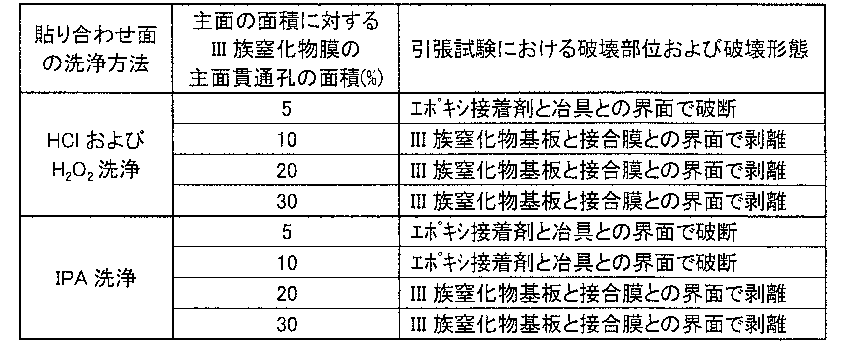
表2を参照して、IPA洗浄を行なったものが、III族窒化物膜の主面貫通孔の面積が主面の面積の10%以下において、接合強度が高かった。また、HClおよびH2O2洗浄ならびにIPA洗浄を行なった接合膜の貼り合わせ面における金属を含む不純物の濃度を、TXRF(全反射蛍光X線)分析により測定した。HClおよびH2O2洗浄を行なったものは、Fe濃度およびNi濃度いずれも1×1010cm-2以下であった。IPA洗浄を行なったものは、Fe濃度が5.7×1011cm-2で、Ni濃度が1.5×1011cm-2であった。
(比較例1)
III族窒化物膜として、導電性向上不純物であるO(酸素)原子が6×1017cm-3の濃度にドーピングされ、両主面が鏡面に研磨された、直径2インチ(5.08cm)で厚さが400μmのGaN膜を1枚準備した。かかるIII族窒化物膜のN原子面である主面に、当該主面から約0.7μmの深さの位置にH(水素)イオンを注入した。Hイオン注入は、加速電圧が100keVで、ドーズ量が5×1017cm-2で行なった。Hイオンを注入したIII族窒化物膜のHイオンが注入された側の主面と、直径が2インチ(5.08cm)で厚さが500μmのムライト基板とを、実施例1と同様の手順で貼り合わせてアニールすることにより、Hイオンが注入された部分でIII族窒化物膜を分離することにより、ムライト基板上に厚さが0.3μmのIII族窒化物膜を有するIII族窒化物複合基板を得た。得られたIII族窒化物複合基板のシート抵抗は、1×10¹⁰Ω/sq以上であった。
III族窒化物膜として、導電性向上不純物であるO(酸素)原子が6×1017cm-3の濃度にドーピングされ、両主面が鏡面に研磨された、直径2インチ(5.08cm)で厚さが400μmのGaN膜を1枚準備した。かかるIII族窒化物膜のN原子面である主面に、当該主面から約0.7μmの深さの位置にH(水素)イオンを注入した。Hイオン注入は、加速電圧が100keVで、ドーズ量が5×1017cm-2で行なった。Hイオンを注入したIII族窒化物膜のHイオンが注入された側の主面と、直径が2インチ(5.08cm)で厚さが500μmのムライト基板とを、実施例1と同様の手順で貼り合わせてアニールすることにより、Hイオンが注入された部分でIII族窒化物膜を分離することにより、ムライト基板上に厚さが0.3μmのIII族窒化物膜を有するIII族窒化物複合基板を得た。得られたIII族窒化物複合基板のシート抵抗は、1×10¹⁰Ω/sq以上であった。
(比較例2)
支持基板として、両主面が鏡面に研磨された直径2インチ(5.08cm)で厚さが300μmのMo基板を用いたこと、Hイオンのドーズ量を3.5×1017cm-2としたこと以外は、比較例1と同様の手順で、Mo基板上に厚さが0.3μmのIII族窒化物膜を有するIII族窒化物複合基板を得た。得られたIII族窒化物複合基板を、N2ガス(窒素ガス)雰囲気中800℃で3時間さらに熱処理することにより、大部分の領域でシート抵抗が6700Ω/sqまで低くなったが、一部の領域では35000Ω/sqと高いままであった。
支持基板として、両主面が鏡面に研磨された直径2インチ(5.08cm)で厚さが300μmのMo基板を用いたこと、Hイオンのドーズ量を3.5×1017cm-2としたこと以外は、比較例1と同様の手順で、Mo基板上に厚さが0.3μmのIII族窒化物膜を有するIII族窒化物複合基板を得た。得られたIII族窒化物複合基板を、N2ガス(窒素ガス)雰囲気中800℃で3時間さらに熱処理することにより、大部分の領域でシート抵抗が6700Ω/sqまで低くなったが、一部の領域では35000Ω/sqと高いままであった。
参考発明Iにかかる参考例I-A~参考例I-Iについて以下に示す。
(参考例I-A)
1.III族窒化物複合基板の作製
図12(A)を参照して、支持基板11として直径75mmのムライト基板を準備し、支持基板11の両主面をダイヤモンド砥粒と銅系定盤を用いた粗研磨、ダイヤモンド砥粒とスズ定盤を用いた中間研磨、不織布研磨パッドを用いた仕上げ研磨によりRMS(二乗平均平方根粗さ)を5nm以下に鏡面化した後、その上に厚さ800nmのSiO2膜をLP-CVD(減圧-化学気相堆積)法により成長させ、平均粒径が40nmのコロイダルシルカ砥粒を含みpHが10のスラリーを用いたCMPにより、主面のRMSが0.3nm以下に平坦化された厚さ400nmの接合膜12aを形成した。CMPで用いた砥粒を除去するために、KOH水溶液による無砥粒ポリシング洗浄および純水による洗浄を行なった。
図12(B)を参照して、III族窒化物膜ドナー基板13Dとして直径75mmで厚さ8mmのGaN結晶体を準備し、III族窒化物膜ドナー基板13Dの貼り合わせ面を機械研磨およびCMPによりRMSを2nm以下に鏡面化した後、その上に厚さ800nmのSiO2膜をLP-CVD(減圧-化学気相堆積)法により成長させ、平均粒径が40nmのコロイダルシルカ砥粒を含みpHが10のスラリーを用いたCMPにより、主面がRMSで0.3nm以下に平坦化された厚さ500nmの接合膜12bを形成した。CMPに用いた砥粒を除去するために、KOH水溶液による無砥粒ポリシング洗浄および純水による洗浄を行なった。ここで、III族窒化物膜ドナー基板13Dは、下地基板としてGaAs基板を用いて、HVPE法により成長させたものであった。
図12(C)を参照して、接合膜12aと接合膜12bとを貼り合わせることにより、支持基板11とIII族窒化物膜13とを接合膜12を介在させて貼り合わせた接合基板1Lを得た。貼り合わせ後に、接合基板1Lを窒素ガス雰囲気中で800℃まで昇温することによりアニールして接合強度を高めた。
図12(D)を参照して、接合基板1LのIII族窒化物膜ドナー基板13Dを接合膜12との貼り合わせ面から内部に180μmの距離の深さに位置する面でワイヤーソーにより切断することにより、支持基板11とIII族窒化物膜13であるGaN膜とが接合膜12を介在させて貼り合わされたIII族窒化物複合基板1を得た。ワイヤーは、ダイヤモンド砥粒を電着した固定砥粒ワイヤーを用いた。切断抵抗を低減して厚さの精度および平坦性を高めるために、切断方式としてはワイヤーを揺動させ、それに同期してIII族窒化物膜ドナー基板13Dを振動させる方式とした。ワイヤーソー切断の抵抗係数は、4200Nとした。切断後に、III族窒化物複合基板1のIII族窒化物膜13を機械研磨およびCMPを行なった。III族窒化物膜13の厚さ、オフ角の均一化のため、CMPでの複合基板の装置への取り付けには、予備的に真空チャック吸着で基板形状を矯正した後に、装置に吸着固定する方式とした。
得られたIII族窒化物複合基板1について、III族窒化物膜13の厚さの平均値mtに対する厚さの標準偏差stの比st/mtおよびIII族窒化物膜13の主面13mの(0001)面に対するオフ角の絶対値の平均値moに対するオフ角の絶対値の標準偏差soの比so/moを表1に示した。ここで、厚さの平均値mt、厚さの標準偏差st、オフ角の絶対値の平均値mo、およびオフ角の絶対値の標準偏差stは、図7に示すIII族窒化物膜13の主面13m上において、1つの中心点PCと、その中心点PCから互いに直角な4方向上でかつ外縁から5mm内側にある4つの外側点POと、1つの中心点PCと4つの外側点POとの中間に位置する4つの点および4つの外側点の互いの中間に位置する4つの点をあわせた8つの中間点PMとで構成される13点の測定点PにおけるIII族窒化物膜13の厚さおよびオフ角の絶対値から算出した。
2.III族窒化物半導体デバイスの作製
図15(A)を参照して、III族窒化物複合基板1のIII族窒化物膜13上に、MOVPE法により、III族窒化物層20として、III族窒化物膜13上に、厚さ5μmのn-GaN層21、厚さ50nmのn-In0.05Ga0.95N層22、厚さ3nmのIn0.14Ga0.86N井戸層と厚さ15nmのGaN障壁層とで構成される3周期の多重量子井戸構造を有する活性層23、厚さ20nmのp-Al0.09Ga0.91N層24、および厚さ150nmのp-GaN層25を順にエピタキシャル成長させることにより、積層III族窒化物複合基板2を得た。その後、RTA(高速熱処理装置)によりアニールして活性化させた。
図15(A)を参照して、III族窒化物複合基板1のIII族窒化物膜13上に、MOVPE法により、III族窒化物層20として、III族窒化物膜13上に、厚さ5μmのn-GaN層21、厚さ50nmのn-In0.05Ga0.95N層22、厚さ3nmのIn0.14Ga0.86N井戸層と厚さ15nmのGaN障壁層とで構成される3周期の多重量子井戸構造を有する活性層23、厚さ20nmのp-Al0.09Ga0.91N層24、および厚さ150nmのp-GaN層25を順にエピタキシャル成長させることにより、積層III族窒化物複合基板2を得た。その後、RTA(高速熱処理装置)によりアニールして活性化させた。
図15(B)を参照して、積層III族窒化物複合基板2のIII族窒化物層20の最上層であるp-GaN層25上に、EB(電子線)蒸着法により、厚さ4nmのNi層および厚さ200nmのAu層を順次形成し、アニールにより合金化することにより第1電極30を形成した。第1電極30上に、EB蒸着法により、厚さ200nmのTi層、厚さ100nmのPt層、および厚さ1000nmのAu層を順次形成することによりパッド電極33を形成した。
また、デバイス支持基板40としてCuW基板を準備し、デバイス支持基板40上に、EB蒸着法により、厚さ200nmのTi層、厚さ100nmのPt層、および厚さ1000nmのAu層を順次形成することによりパッド電極43を形成した。パッド電極43上に、接合金属膜44としてAuSnはんだ膜を形成した。
次に、パッド電極33に接合金属膜44を貼り合わせることにより、積層基板3を得た。
図15(C)を参照して、積層基板3から、III族窒化物複合基板1の支持基板11および接合膜12を、フッ化水素酸を用いて、エッチングにより除去した。
図15(D)を参照して、積層基板3から支持基板11および接合膜12が除去されて露出したIII族窒化物膜13上に、EB蒸着法により、厚さ20nmのTi層、厚さ200nmのAl層、および厚さ300nmのAu層を順次形成し、アニールすることにより、第2電極50を形成した。また、デバイス支持基板40上に、EB蒸着法により、厚さ20nmのTi層、および厚さ300nmのAu層を順次形成し、アニールすることにより、デバイス支持基板電極45を形成した。こうして、III族窒化物半導体デバイス4が得られた。
得られたIII族窒化物半導体デバイス4について、光出力を、積分球を用いて、注入電流4Aの条件で測定した。発光素子の光出力は、以下のように測定した。すなわち、積分球内に載置された発光素子に所定の電流を注入し、その発光素子から集光された光を受けるディテクタによって光出力を測定した。そして、光出力が2W以上の基準に適合したものを良品、適合しなかったものを不良品とし、良品を表品と不良品との合計で除したものの百分率を歩留率とした。III族窒化物半導体デバイスの歩留率を表3にまとめた。
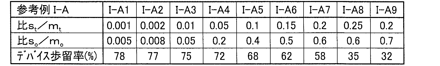
表3を参照して、厚さ150μmのIII族窒化物膜を有する直径75mmのIII族窒化物複合基板であって、III族窒化物膜の厚さの平均値mtに対する厚さの標準偏差stの比st/mtが0.001以上0.2以下であり、III族窒化物膜の主面の(0001)面に対するオフ角の絶対値の平均値moに対するオフ角の絶対値の標準偏差soの比so/moが0.005以上0.6以下のIII族窒化物複合基板を用いて作製されたIII族窒化物半導体デバイスの歩留が高かった。なお、参考例I-A1においては、厚さ分布およびオフ角分布を低減するために、切断および研磨の際に高度な制御が必要となり、切断および研磨に長時間を要した。
(参考例I-B)
図12および図15を参照して、支持基板11としてムライト-YSZ基板(基板全体に対してムライトが70質量%でYSZが30質量%であり、YSZに対してZrO2が90モル%でY2O3が10モル%である)を用いて、直径がそれぞれ75mm、100mm、125mm、および150mmのIII族窒化物複合基板1を作製したこと以外は、参考例I-Aと同様にして、III族窒化物複合基板1およびIII族窒化物半導体デバイス4を作製した。
図12および図15を参照して、支持基板11としてムライト-YSZ基板(基板全体に対してムライトが70質量%でYSZが30質量%であり、YSZに対してZrO2が90モル%でY2O3が10モル%である)を用いて、直径がそれぞれ75mm、100mm、125mm、および150mmのIII族窒化物複合基板1を作製したこと以外は、参考例I-Aと同様にして、III族窒化物複合基板1およびIII族窒化物半導体デバイス4を作製した。
参考例I-Aと同様にして、III族窒化物複合基板1について、III族窒化物膜13の厚さの平均値mtに対する厚さの標準偏差stの比st/mtおよびIII族窒化物膜の主面の(0001)面に対するオフ角の絶対値の平均値moに対するオフ角の絶対値の標準偏差soの比so/moを算出して、表2にまとめた。また、参考例I-Aと同様にして、III族窒化物半導体デバイス4の歩留率を算出して、表4にまとめた。
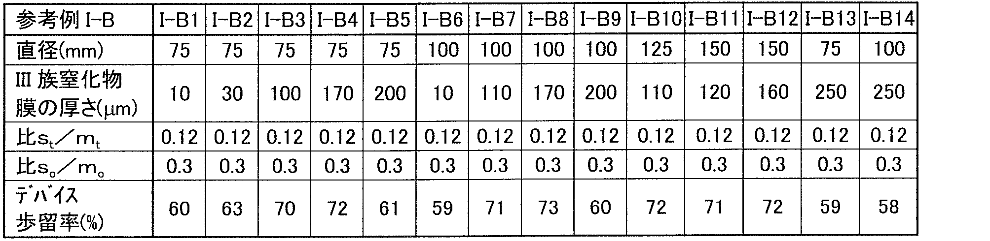
表4を参照して、厚さ10μm~250μmのIII族窒化物膜を有する直径75mm~150mmのIII族窒化物複合基板であって、III族窒化物膜の厚さの平均値mtに対する厚さの標準偏差stの比st/mtが0.001以上0.2以下の0.12であり、III族窒化物膜の主面の(0001)面に対するオフ角の絶対値の平均値moに対するオフ角の絶対値の標準偏差soの比so/moが0.005以上0.6以下の0.3であるIII族窒化物複合基板を用いて作製されたIII族窒化物半導体デバイスの歩留が高かった。
(参考例I-C)
半導体デバイス用基板として、III族窒化物自立基板(以下、FS基板ともいう)、イオン注入法により作製されたIII族窒化物複合基板(以下、BP基板ともいう)、および本発明の参考形態I-4により作製されたIII族窒化物複合基板(以下、BS基板ともいう)を準備した。
半導体デバイス用基板として、III族窒化物自立基板(以下、FS基板ともいう)、イオン注入法により作製されたIII族窒化物複合基板(以下、BP基板ともいう)、および本発明の参考形態I-4により作製されたIII族窒化物複合基板(以下、BS基板ともいう)を準備した。
FS基板は、所定の直径を有するGaN結晶体をワイヤーソーで切断し研磨することにより表3に示す直径および厚さの基板とした。
BP基板は、図17(B)に示すように、III族窒化物膜ドナー基板13Dである所定の直径を有するGaN結晶体にその主面から内部に所定の深さの位置に水素イオンを注入することによりイオン注入領域13iを形成した後、図17(C)に示すように、支持基板11とIII族窒化物膜ドナー基板13Dのイオン注入領域13i側とを接合膜12を介在させて貼り合わせた後、図17(D)に示すように、850℃でアニールすることにより、III族窒化物膜ドナー基板13Dをそのイオン注入領域13iで分離することにより、表5に示す直径およびIII族窒化物膜の厚さの基板とした。ここで、支持基板11としては、ムライト基板を用いた。
BS基板は、支持基板としてムライト基板を用いたこと以外は、参考例I-Bと同様にして、表3に示す直径およびIII族窒化物膜の厚さの基板とした。
上記のFS基板、BP基板、およびBS基板を用いたこと以外は、参考例I-Bと同様にして、III族窒化物複合基板1およびIII族窒化物半導体デバイス4を作製した。
参考例I-Aと同様にして、III族窒化物複合基板1について、III族窒化物膜13の厚さの平均値mtに対する厚さの標準偏差stの比st/mtおよびIII族窒化物膜の主面の(0001)面に対するオフ角の絶対値の平均値moに対するオフ角の絶対値の標準偏差soの比so/moを算出して、表5にまとめた。また、参考例I-Aと同様にして、III族窒化物半導体デバイス4の歩留率を算出して、表5にまとめた。

表5を参照して、直径50mm~125mmで厚さ200μm~500μmのFS基板を用いて作製したIII族窒化物半導体デバイスは、直径が大きく厚さが小さいものは反りが大きくまた割れが発生しやすく、いずれも歩留率が60%に満たなかった。
また、直径が75mm~125mmでIII族窒化物膜の厚さが0.5μmのBP基板を用いて作製したIII族窒化物半導体デバイスは、III族窒化物膜の厚さが小さいため、良好なデバイス特性が発現せず、歩留率が低下した。
これらに対して、BS基板を用いて作製したIII族窒化物半導体デバイスは、歩留率が65%以上と高かった。
(参考例I-D)
支持基板としてAl2O3-SiO2複合酸化物基板(基板全体に対してAl2O3が85質量%でSiO2が15質量%である)を用いたこと以外は、参考例I-Bと同様の要領で作製した複数のIII族窒化物複合基板の反りおよびTTVを測定したところ、表6に示すとおりであった。ここで、III族窒化物複合基板の反りおよびTTVは、光干渉式のフラットネステスターにより測定した。
支持基板としてAl2O3-SiO2複合酸化物基板(基板全体に対してAl2O3が85質量%でSiO2が15質量%である)を用いたこと以外は、参考例I-Bと同様の要領で作製した複数のIII族窒化物複合基板の反りおよびTTVを測定したところ、表6に示すとおりであった。ここで、III族窒化物複合基板の反りおよびTTVは、光干渉式のフラットネステスターにより測定した。
これらのIII族窒化物複合基板を用いて、参考例I-Bと同様にして、III族窒化物半導体デバイスを作製した。
III族窒化物複合基板について、III族窒化物膜の厚さの平均値mtに対する厚さの標準偏差stの比st/mtおよびIII族窒化物膜の主面の(0001)面に対するオフ角の絶対値の平均値moに対するオフ角の絶対値の標準偏差soの比so/mo、ならびにIII族窒化物複合基板の反りおよびTTVを表6にまとめた。また、参考例I-Aと同様にして、III族窒化物半導体デバイス4の歩留率を算出して、表6にまとめた。
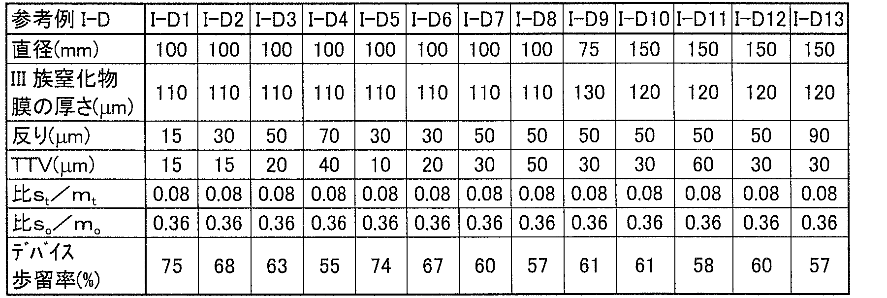
表6を参照して、III族窒化物膜側の主面における反りが50μm以下であり、TTVが30μm以下であるIII族窒化物複合基板を用いて作製したIII族窒化物半導体デバイスは、歩留率が高かった。
(参考例I-E)
支持基板の熱膨張係数αSに対するIII族窒化物膜の熱膨張係数αIII-Nの比αIII-N/αSが異なり、かつ、支持基板の厚さtSに対するIII族窒化物膜の厚さtIII-Nの比tIII-N/tSが異なる複数のIII族窒化物複合基板を用いたこと以外は、参考例I-Bと同様にして、III族窒化物半導体デバイスを作製した。ここで、上記の比を変化させるために、下地基板として厚さの異なるムライト基板、ムライト-YSZ基板、Al2O3-SiO2複合酸化物基板を用いた。
支持基板の熱膨張係数αSに対するIII族窒化物膜の熱膨張係数αIII-Nの比αIII-N/αSが異なり、かつ、支持基板の厚さtSに対するIII族窒化物膜の厚さtIII-Nの比tIII-N/tSが異なる複数のIII族窒化物複合基板を用いたこと以外は、参考例I-Bと同様にして、III族窒化物半導体デバイスを作製した。ここで、上記の比を変化させるために、下地基板として厚さの異なるムライト基板、ムライト-YSZ基板、Al2O3-SiO2複合酸化物基板を用いた。
支持基板の熱膨張係数αSに対するIII族窒化物膜の熱膨張係数αIII-Nの比αIII-N/αSおよび支持基板の厚さtSに対するIII族窒化物膜の厚さtIII-Nの比tIII-N/tS、ならびにIII族窒化物半導体デバイスの歩留率を表7にまとめた。

表7を参照して、支持基板の熱膨張係数αSに対するIII族窒化物膜の熱膨張係数αIII-Nの比αIII-N/αSが0.75以上1.25以下であり、支持基板の厚さtSに対するIII族窒化物膜の厚さtIII-Nの比tIII-N/tSが0.02以上1以下であるIII族窒化物複合基板を用いて作製したIII族窒化物半導体デバイスの歩留率は高かった。
(参考例I-F)
洗浄条件を調節することによって、III族窒化物膜の表面における不純物金属原子の量を調整したこと以外は、参考例I-Bと同様にして、III族窒化物複合基板およびIII族窒化物半導体デバイスを作製した。III族窒化物複合基板の直径およびIII族窒化物膜の表面における不純物金属原子の量、ならびにIII族窒化物半導体デバイスの歩留率を表8にまとめた。ここで、III族窒化物膜の表面における不純物金属原子の量は、TXRF(全反射蛍光X線)法により測定した。ここで、TXRF法による測定は、タングステン(W)線源を用いて、0.05°の入射角の条件で行なった。
洗浄条件を調節することによって、III族窒化物膜の表面における不純物金属原子の量を調整したこと以外は、参考例I-Bと同様にして、III族窒化物複合基板およびIII族窒化物半導体デバイスを作製した。III族窒化物複合基板の直径およびIII族窒化物膜の表面における不純物金属原子の量、ならびにIII族窒化物半導体デバイスの歩留率を表8にまとめた。ここで、III族窒化物膜の表面における不純物金属原子の量は、TXRF(全反射蛍光X線)法により測定した。ここで、TXRF法による測定は、タングステン(W)線源を用いて、0.05°の入射角の条件で行なった。
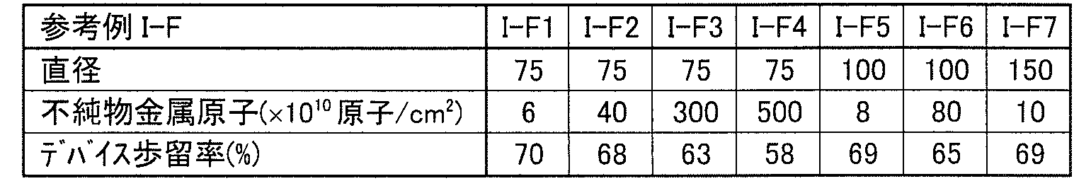
表8を参照して、III族窒化物膜の主面における不純物金属原子が3×10¹²原子/cm2以下であるIII族窒化物複合基板を用いた作製したIII族窒化物半導体デバイスの歩留率は高かった。
(参考例I-G)
支持基板としてムライト基板を用い、III族窒化物膜ドナー基板として、ドーパントとしてOおよびSiが添加され、転位密度が4×106cm-2でキャリア濃度が2×1018cm-3である、転位集中領域のない均一なGaN結晶体を用いたこと以外は、参考例I-Bと同様にして、III族窒化物複合基板およびIII族窒化物半導体デバイスを作製した。ここで、研磨条件を調整することにより、III族窒化物膜および支持基板の主面の最大RMSを調整した。
支持基板としてムライト基板を用い、III族窒化物膜ドナー基板として、ドーパントとしてOおよびSiが添加され、転位密度が4×106cm-2でキャリア濃度が2×1018cm-3である、転位集中領域のない均一なGaN結晶体を用いたこと以外は、参考例I-Bと同様にして、III族窒化物複合基板およびIII族窒化物半導体デバイスを作製した。ここで、研磨条件を調整することにより、III族窒化物膜および支持基板の主面の最大RMSを調整した。
III族窒化物複合基板におけるIII族窒化物膜および支持基板の主面の最大RMS、ならびにIII族窒化物半導体デバイスの歩留率を表9にまとめた。
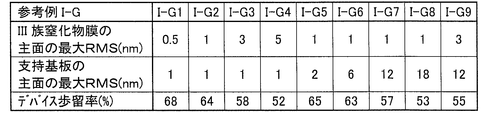
表9を参照して、III族窒化物膜の主面のRMSが3nm以下であり、支持基板の主面のRMSが12nm以下であるIII族窒化物複合基板を用いて作製したIII族窒化物半導体デバイスの歩留率は高かった。
(参考例I-H)
支持基板としてAl2O3-SiO2複合酸化物基板(基板全体に対してAl2O3が82質量%でSiO2が18質量%である)を用い、III族窒化物膜ドナー基板として、ドーパントとしてFeが添加され比抵抗が1×10⁷Ωcmである半絶縁性のGaN結晶体を用いたこと以外は、参考例I-Bと同様にして、III族窒化物複合基板を作製した。ここで、研磨条件を調整することにより、III族窒化物複合基板のIII族窒化物膜の主面のRMSの平均値mIII-Nおよび標準偏差sIII-N、ならびに支持基板の主面のRMSの平均値mSおよび標準偏差sSを調整した。
支持基板としてAl2O3-SiO2複合酸化物基板(基板全体に対してAl2O3が82質量%でSiO2が18質量%である)を用い、III族窒化物膜ドナー基板として、ドーパントとしてFeが添加され比抵抗が1×10⁷Ωcmである半絶縁性のGaN結晶体を用いたこと以外は、参考例I-Bと同様にして、III族窒化物複合基板を作製した。ここで、研磨条件を調整することにより、III族窒化物複合基板のIII族窒化物膜の主面のRMSの平均値mIII-Nおよび標準偏差sIII-N、ならびに支持基板の主面のRMSの平均値mSおよび標準偏差sSを調整した。
さらに、図10を参照して、以下のようにして、III族窒化物半導体デバイス4として、HEMTを作製した。
まず、III族窒化物複合基板1のIII族窒化物膜13上に、MOVPE法により、III族窒化物層20として、厚さ1.5μmのGaN層26、厚さ30nmのAl0.2Ga0.8N層27を順にエピタキシャル成長させることにより、積層III族窒化物複合基板2を得た。
次に、Al0.2Ga0.8N層27上にフォトリソグラフィ、EB蒸着、およびリフトオフによって、ソース電極60およびドレイン電極70を作製した。これらの電極には、厚さ20nmのTi層、厚さ100nmのAl層、厚さ20nmのTi層、および厚さ300nmのAu層を順次形成し、リフトオフした後、600℃で1分間のアニールにより合金化した。
次に、ソース電極60およびドレイン電極70の作製と同様の工程により、ゲート電極80を作製した。ゲート電極80の作製においては、厚さ50nmNi層および厚さ500nmのAu層を順次形成した。ゲート長は2μmとした。
こうして得られたIII族窒化物半導体デバイス4であるHEMTは、III族窒化物複合基板1のIII族窒化物膜13上に、少なくとも1層のIII族窒化物層20としてGaN層26およびAl0.2Ga0.8N層27が形成され、Al0.2Ga0.8N層27上にソース電極60、ドレイン電極70、およびゲート電極80が、お互いに分離され、かつ、ゲート電極80がソース電極60とドレイン電極70との間に位置するように、配置されていた。
得られたHEMTのリークするゲート電流密度を検査した。具体的には、5Vのゲート電圧を与えたときに、リークしたゲート電流密度が1×10⁻⁶A/cm2以下の基準に適合したものを良品、適合しなかったものを不良品とし、良品を良品と不良品の合計で除したものの百分率を歩留率とした。
III族窒化物複合基板におけるIII族窒化物膜の主面のRMSの平均値mIII-Nおよび標準偏差sIII-N、および支持基板の主面のRMSの平均値mSおよび標準偏差sS、ならびにIII族窒化物半導体デバイスの歩留率を表10にまとめた。

表10を参照して、III族窒化物膜の主面は、そのRMSの平均値mIII-Nが0.1nm以上2nm以下でありそのRMSの標準偏差sIII-Nが0.4nm以下であり、支持基板の主面は、そのRMSの平均値mSが0.3nm以上10nm以下であり、そのRMSの標準偏差sSが3nm以下であるIII族窒化物複合基板を用いて作製したIII族窒化物半導体デバイスの歩留率は高かった。
(参考例I-I)
1.III族窒化物複合基板の作製
図14(A)~(C)を参照して、支持基板11として直径100mmのAl2O3-SiO2複合酸化物基板(基板全体に対してAl2O3が88質量%でSiO2が12質量%である)を準備したこと、III族窒化物膜ドナー基板13Dとして直径100mmで厚さが400μmのGaN結晶基板を準備したこと、支持基板11およびIII族窒化物膜ドナー基板13Dのそれぞれの主面上にPE-CVD法により厚さ500nmのSiO2膜を成長させた後、平均粒径が20nmのコロイダルシリカを含みpHが9のスラリー用いたCMPにより主面がRMSで0.15nm以下に平坦化された厚さ250nmの接合膜12a,12bを形成したこと、純水による洗浄として純水とPVA(ポリビニルアルコール)製スポンジとを用いたスクラブ洗浄を行なったこと、以外は参考例I-Aと同様にして接合基板1Lを得た。
図14(D)を参照して、接合基板1LのIII族窒化物膜ドナー基板13Dの貼り合わせ主面と反対側の主面から研削および研磨を行なった。研削においては、平均粒径が25μm~35μmのダイヤモンド砥粒を含むビトリファイド砥石を用いた。研磨においては、平均粒径が3μm、2μm、0.25μmのダイヤモンド砥粒をそれぞれ含むスラリーを用いて段階的に機械研磨を実施した。かかる研磨は、厚み分布およびオフ角分布を低減するため、予備的に機械加圧で基板の反りを矯正した状態で保持プレートに貼り付けて実施した。研磨後にICP-RIE(誘導結合プラズマ-反応性イオンエッチング)法により発生させた塩素ガスプラズマによるドライエッチング処理を実施した。なお、参考例I-I8については、上記の研削の代わりに平均粒径が9μmのダイヤモンド砥粒を用いた粗研磨を実施した。こうして、厚さが150μmのIII族窒化物膜13を含むIII族窒化物複合基板1を得た。
2.III族窒化物半導体デバイスの作製
図15を参照して、本参考例におけるIII族窒化物複合基板1を用いたこと、積層基板3からの支持基板11および接合膜12の除去を平均粒径が35μm~45μmのダイヤモンド砥粒を含むビトリファイド砥石を用いた研削により実施したこと、特に参考例I-I9については平均粒径が15μmのダイヤモンド砥粒を用いた研磨により実施したこと、かかる研削および/または研磨後に接合膜及び支持基板の残渣の除去のため、フッ化水素酸によるエッチング洗浄したこと以外は、参考例I-Aと同様にしてIII族窒化物半導体デバイス4を得た。
図15を参照して、本参考例におけるIII族窒化物複合基板1を用いたこと、積層基板3からの支持基板11および接合膜12の除去を平均粒径が35μm~45μmのダイヤモンド砥粒を含むビトリファイド砥石を用いた研削により実施したこと、特に参考例I-I9については平均粒径が15μmのダイヤモンド砥粒を用いた研磨により実施したこと、かかる研削および/または研磨後に接合膜及び支持基板の残渣の除去のため、フッ化水素酸によるエッチング洗浄したこと以外は、参考例I-Aと同様にしてIII族窒化物半導体デバイス4を得た。
参考例I-Aと同様にして、III族窒化物複合基板1について、III族窒化物膜13の厚さの平均値mtに対する厚さの標準偏差stの比st/mtおよびIII族窒化物膜の主面の(0001)面に対するオフ角の絶対値の平均値moに対するオフ角の絶対値の標準偏差soの比so/moを算出して、表11にまとめた。また、参考例I-Aと同様にして、III族窒化物半導体デバイス4の歩留率を算出して、表11にまとめた。

表11を参照して、III族窒化物膜の厚さの平均値mtに対する厚さの標準偏差stの比st/mtが0.001以上0.2以下であり、III族窒化物膜の主面の(0001)面に対するオフ角の絶対値の平均値moに対するオフ角の絶対値の標準偏差soの比so/moが0.005以上0.6以下であるIII族窒化物複合基板を用いて作製されたIII族窒化物半導体デバイスの歩留が高かった。なお、参考例I-I1においては、厚さ分布およびオフ角分布を低減するために、研削および研磨の際に高度な制御が必要となり、研削および研磨に長時間を要した。
参考発明IIにかかる参考例II-A~参考例II-Hについて以下に示す。
(参考例II-A)
1.III族窒化物複合基板の作製
図12(A)を参照して、支持基板11として直径75mmで厚さ300μmのAl2O3-SiO2複合酸化物基板(基板全体に対してAl2O3が85質量%でSiO2が15質量%である)を準備した。支持基板11は、その熱伝導率が10W・m-1・K-1であり、そのヤング率が250GPaであった。支持基板11の両側の主面11m,11nを、研磨剤としてダイヤモンドスラリーを用いて、銅系定盤により粗研磨、スズ定盤により中間研磨、格子溝を形成した不織布研磨パッドにより仕上げ研磨を行なった。仕上げ研磨においては、作用係数FEが4×10-17m2/s以上1×10-16m2/s以下の条件で研磨した。
次に、支持基板11の仕上げ研磨後の主面11m上に、厚さ800nmのSiO2膜をPE-CVD(プラズマ援用-化学気相堆積)法により成長させ、窒素雰囲気中で800℃で1時間のアニールを行なった後に、平均粒径40nmのコロイダルシリカ砥粒を含みpHが10のスラリーを用いたCMP(化学機械的研磨)により、主面12amがRMS(二乗平均平方根粗さ)で0.3nm以下に鏡面化された厚さ400nmの接合膜12aを形成した。次いで、CMPで用いたコロイダルシリカ砥粒を除去するために、KOH水溶液による無砥粒ポリシング洗浄、純水によるポリシング洗浄、および純水によるメガソニック洗浄(500kHz~5MHzのメガソニック帯域の周波数の超音波を用いた洗浄)を行なった。
また、図12(B)を参照して、III族窒化物膜ドナー基板13Dとして直径75mmで厚さ8mmのGaN結晶体を準備し、III族窒化物膜ドナー基板13Dの貼り合わせ面を機械研磨およびCMPによりRMSを2nm以下に平坦化した後、その上に厚さ800nmのSiO2膜をPE-CVD法により成長させ、窒素雰囲気中で800℃で1時間のアニールを行なった後に、平均粒径が40nmのコロイダルシルカ砥粒を含みpHが10のスラリーを用いたCMPにより、主面12bnがRMSで0.3nm以下に鏡面化された厚さ500nmの接合膜12bを形成した。次いで、CMPで用いたコロイダルシリカ砥粒を除去するために、KOH水溶液による無砥粒ポリシング洗浄、純水によるポリシング洗浄、および純水によるメガソニック洗浄(500kHz~5MHzのメガソニック帯域の周波数の超音波を用いた洗浄)を行なった。ここで、III族窒化物膜ドナー基板13Dは、下地基板としてGaAs基板を用いて、HVPE法により成長させたものであった。III族窒化物膜ドナー基板13Dは、その導電型がn型で、その転位密度が1×108cm-2で、そのキャリア濃度が1×10¹⁷であった。
次に、図12(C)を参照して、接合膜12aの主面12amと接合膜12bの主面12bnとを貼り合わせることにより、支持基板11とIII族窒化物膜13とを接合膜12を介在させて貼り合わせた接合基板1Lを得た。貼り合わせ後に、接合基板1Lを窒素ガス雰囲気中で800℃まで昇温することによりアニールして接合強度を高めた。
次に、図12(D)を参照して、接合基板1LのIII族窒化物膜ドナー基板13Dを接合膜12との貼り合わせ面から内部に150μmの距離の深さに位置する面でワイヤーソーにより切断することにより、支持基板11とIII族窒化物膜13であるGaN膜とが接合膜12を介在させて貼り合わされたIII族窒化物複合基板1を得た。ワイヤーは、ダイヤモンド砥粒を電着した線径180μmの固定砥粒ワイヤーを用いた。切断抵抗を低減して厚さの精度および平坦性を高めるために、切断方式としてはワイヤーを揺動させ、それに同期してIII族窒化物膜ドナー基板13Dを振動させる方式とした。ワイヤーソー切断の抵抗係数は、4200Nとした。切断後に、III族窒化物複合基板1のIII族窒化物膜13を機械研磨およびCMPを行なった。III族窒化物膜13の厚さの均一化のため、CMPでの複合基板の装置への取り付けには、予備的に真空チャック吸着で基板形状を矯正した後に、装置に吸着固定する方式とした。
次に、得られたIII族窒化物複合基板1のIII族窒化物膜13側の主面13mを、研磨剤としてダイヤモンドスラリーを用いて、銅系定盤により粗研磨、スズ定盤により中間研磨を実施した。さらに、研磨剤としてコロイダルシリカ砥粒を含むpHが11のスラリーを用いて不織布研磨パッドにより仕上げ研磨を行なった。仕上げ研磨においては、作用係数FEが6×10-14m2/sの条件で研磨した。仕上げ研磨後のIII族窒化物膜13の厚さは110μmであった。
上記仕上げ研磨後のIII族窒化物複合基板1について、支持基板11側の主面11nのRMSの平均値mS、支持基板11側の主面11nのRMSの平均値mSに対するRMSの標準偏差sSの比sS/mSを表12にまとめた。
ここで、RMSの平均値mSおよびRMSの平均値mSに対するRMSの標準偏差sSの比sS/mSは、図7に示す支持基板11側の主面11n上において、1つの中心点PCと、その中心点PCから互いに直角な4方向上でかつ外縁から5mm内側にある4つの外側点POと、1つの中心点PCと4つの外側点POとの中間に位置する4つの点および4つの外側点の互いの中間に位置する4つの点をあわせた8つの中間点PMとで構成される13点の測定点Pにおける支持基板11側の主面11nのRMSから算出した。
2.III族窒化物半導体デバイスの作製
図15(A)を参照して、III族窒化物複合基板1のIII族窒化物膜13側の主面13m上に、MOVPE法により、III族窒化物層20として、III族窒化物膜13上に、厚さ5μmのn-GaN層21、厚さ50nmのn-In0.05Ga0.95N層22、厚さ3nmのIn0.14Ga0.86N井戸層と厚さ15nmのGaN障壁層とで構成される3周期の多重量子井戸構造を有する活性層23、厚さ20nmのp-Al0.09Ga0.91N層24、および厚さ150nmのp-GaN層25を順にエピタキシャル成長させることにより、積層III族窒化物複合基板2を得た。その後、RTA(高速熱処理装置)によりアニールして活性化させた。
図15(A)を参照して、III族窒化物複合基板1のIII族窒化物膜13側の主面13m上に、MOVPE法により、III族窒化物層20として、III族窒化物膜13上に、厚さ5μmのn-GaN層21、厚さ50nmのn-In0.05Ga0.95N層22、厚さ3nmのIn0.14Ga0.86N井戸層と厚さ15nmのGaN障壁層とで構成される3周期の多重量子井戸構造を有する活性層23、厚さ20nmのp-Al0.09Ga0.91N層24、および厚さ150nmのp-GaN層25を順にエピタキシャル成長させることにより、積層III族窒化物複合基板2を得た。その後、RTA(高速熱処理装置)によりアニールして活性化させた。
図15(B)を参照して、積層III族窒化物複合基板2のIII族窒化物層20の最上層であるp-GaN層25上に、EB(電子線)蒸着法により、厚さ4nmのNi層および厚さ200nmのAu層を順次形成し、アニールにより合金化することにより第1電極30を形成した。第1電極30上に、EB蒸着法により、厚さ200nmのTi層、厚さ100nmのPt層、および厚さ1000nmのAu層を順次形成することによりパッド電極33を形成した。
また、デバイス支持基板40としてCuW基板を準備し、デバイス支持基板40上に、EB蒸着法により、厚さ200nmのTi層、厚さ100nmのPt層、および厚さ1000nmのAu層を順次形成することによりパッド電極43を形成した。パッド電極43上に、接合金属膜44としてAuSnはんだ膜を形成した。
次に、パッド電極33に接合金属膜44を貼り合わせることにより、積層基板3を得た。
図15(C)を参照して、積層基板3から、III族窒化物複合基板1の支持基板11および接合膜12を、フッ化水素酸を用いて、エッチングにより除去した。
図15(D)を参照して、積層基板3から支持基板11および接合膜12が除去された露出したIII族窒化物膜13上に、EB蒸着法により、厚さ20nmのTi層、厚さ200nmのAl層、および厚さ300nmのAu層を順次形成し、アニールすることにより、第2電極50を形成した。また、デバイス支持基板40上に、EB蒸着法により、厚さ20nmのTi層、および厚さ300nmのAu層を順次形成し、アニールすることにより、デバイス支持基板電極45を形成した。こうして、III族窒化物半導体デバイス4が得られた。
得られたIII族窒化物半導体デバイス4について、光出力を、積分球を用いて、注入電流4Aの条件で測定した。発光素子の光出力は、以下のように測定した。すなわち、積分球内に載置された発光素子に所定の電流を注入し、その発光素子から集光された光を受けるディテクタによって光出力を測定した。そして、光出力が2W以上の基準に適合したものを良品、適合しなかったものを不良品とし、良品を表品と不良品との合計で除したものの百分率を歩留率とした。III族窒化物半導体デバイスの歩留率を表12にまとめた。
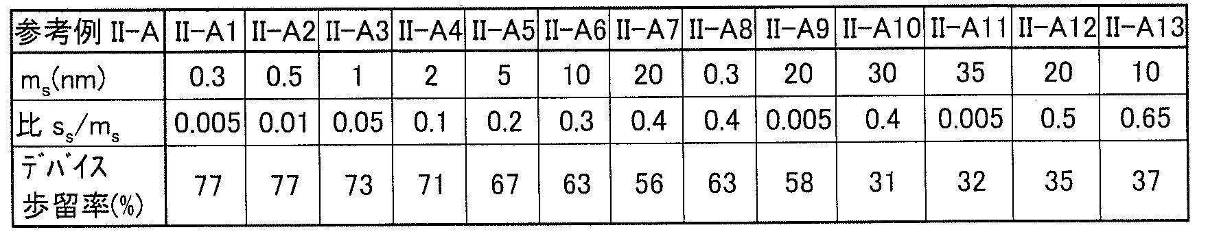
表12を参照して、支持基板と、厚さ110μm(この値は10μm以上250μm以下)のIII族窒化物膜と、を有する直径75mm(この値は75mm以上)のIII族窒化物複合基板であって、支持基板側の主面のRMSの平均値mSが0.3nm以上20nm以下であり、前記支持基板側の主面のRMSの平均値mSに対するRMSの標準偏差sSの比sS/mSが0.005以上0.4以下であるIII族窒化物複合基板を用いて作製されたIII族窒化物半導体デバイスの歩留が高かった。
(参考例II-B)
図12および図15を参照して、支持基板11としてムライト-YSZ基板(基板全体に対してムライトが70質量%でYSZが30質量%であり、ムライトに対してAl2O3が60モル%でSiO2が40モル%であり、YSZに対してZrO2が90モル%でY2O3が10モル%である)を用いたこと、直径をそれぞれ75mm~150mmの間で変動させ、支持基板11側の主面11nの仕上げ研磨においては作用係数FEが6.2×10⁻¹⁷m2/sの条件で研磨したこと、仕上げ研磨後のIII族窒化物膜13の厚さをそれぞれ10μm~250μmの間で変動させた1III族窒化物複合基板1を作製したこと、以外は、参考例II-Aと同様にして、III族窒化物複合基板1およびIII族窒化物半導体デバイス4を作製した。支持基板11は、熱伝導率が30W・m-1・K-1で、ヤング率が150GPaであった。
図12および図15を参照して、支持基板11としてムライト-YSZ基板(基板全体に対してムライトが70質量%でYSZが30質量%であり、ムライトに対してAl2O3が60モル%でSiO2が40モル%であり、YSZに対してZrO2が90モル%でY2O3が10モル%である)を用いたこと、直径をそれぞれ75mm~150mmの間で変動させ、支持基板11側の主面11nの仕上げ研磨においては作用係数FEが6.2×10⁻¹⁷m2/sの条件で研磨したこと、仕上げ研磨後のIII族窒化物膜13の厚さをそれぞれ10μm~250μmの間で変動させた1III族窒化物複合基板1を作製したこと、以外は、参考例II-Aと同様にして、III族窒化物複合基板1およびIII族窒化物半導体デバイス4を作製した。支持基板11は、熱伝導率が30W・m-1・K-1で、ヤング率が150GPaであった。
参考例II-Aと同様にして、III族窒化物複合基板1について、支持基板11側の主面11nのRMSの平均値mS、支持基板11側の主面11nのRMSの平均値mSに対するRMSの標準偏差sSの比sS/mSを算出して、表13にまとめた。また、参考例II-Aと同様にして、III族窒化物半導体デバイス4の歩留率を算出して、表13にまとめた。

表13を参照して、厚さ10μm~250μmのIII族窒化物膜を有する直径75mm~150mmのIII族窒化物複合基板であって、支持基板側の主面のRMSの平均値mSが6nm(この値は0.3nm以上20nm以下)であり、支持基板側の主面のRMSの平均値mSに対するRMSの標準偏差sSの比sS/mSが0.23(この値は0.005以上0.4以下)であるIII族窒化物複合基板を用いて作製されたIII族窒化物半導体デバイスの歩留が高かった。
(参考例II-C)
半導体デバイス用基板として、III族窒化物自立基板(以下、FS基板ともいう)、イオン注入法により作製されたIII族窒化物複合基板(以下、BP基板ともいう)、および参考発明IIの参考形態II-4により作製されたIII族窒化物複合基板(以下、BS基板ともいう)を準備した。
半導体デバイス用基板として、III族窒化物自立基板(以下、FS基板ともいう)、イオン注入法により作製されたIII族窒化物複合基板(以下、BP基板ともいう)、および参考発明IIの参考形態II-4により作製されたIII族窒化物複合基板(以下、BS基板ともいう)を準備した。
FS基板は、所定の直径を有するGaN結晶体をワイヤーソーで切断し研磨することにより表3に示す直径および厚さの基板とした。
BP基板は、図17(B)に示すように、III族窒化物膜ドナー基板13Dである所定の直径を有するGaN結晶体にその主面13nから内部に所定の深さの位置に水素イオンを注入することによりイオン注入領域13iを形成した後、図17(C)に示すように、支持基板11とIII族窒化物膜ドナー基板13Dのイオン注入領域13i側とを接合膜12を介在させて貼り合わせた後、図17(D)に示すように、700℃でアニールすることにより、III族窒化物膜ドナー基板13Dをそのイオン注入領域13iで分離することにより、表14に示す直径およびIII族窒化物膜の厚さの基板とした。ここで、支持基板11としては、Al2O3-SiO2複合酸化物基板(基板全体に対してAl2O3が85質量%でSiO2が15質量%である)を用いた。
BS基板は、支持基板としてAl2O3-SiO2複合酸化物基板(基板全体に対してAl2O3が85質量%でSiO2が15質量%である)を用いたこと以外は、参考例II-Bと同様にして、表14に示す直径およびIII族窒化物膜の厚さの基板とした。
上記のFS基板、BP基板、およびBS基板を用いたこと、支持基板11側の主面11nの仕上げ研磨においては作用係数FEが4.0×10⁻¹⁷m2/sの条件で研磨したこと以外は、参考例II-Bと同様にして、III族窒化物複合基板1およびIII族窒化物半導体デバイス4を作製した。
参考例II-Aと同様にして、III族窒化物複合基板1であるBP基板およびBS基板について、反りW、比W/D、支持基板11側の主面11nのRMSの平均値mS、支持基板11側の主面11nのRMSの平均値mSに対するRMSの標準偏差sSの比sS/mSを算出して、表14にまとめた。また、FS基板について、反りW、比W/D、その裏面側の主面のRMSの平均値mS、裏面側の主面11nのRMSの平均値mSに対するRMSの標準偏差sSの比sS/mSを算出して、表14にまとめた。さらに、参考例II-Aと同様にして、III族窒化物半導体デバイス4の歩留率を算出して、表14にまとめた。
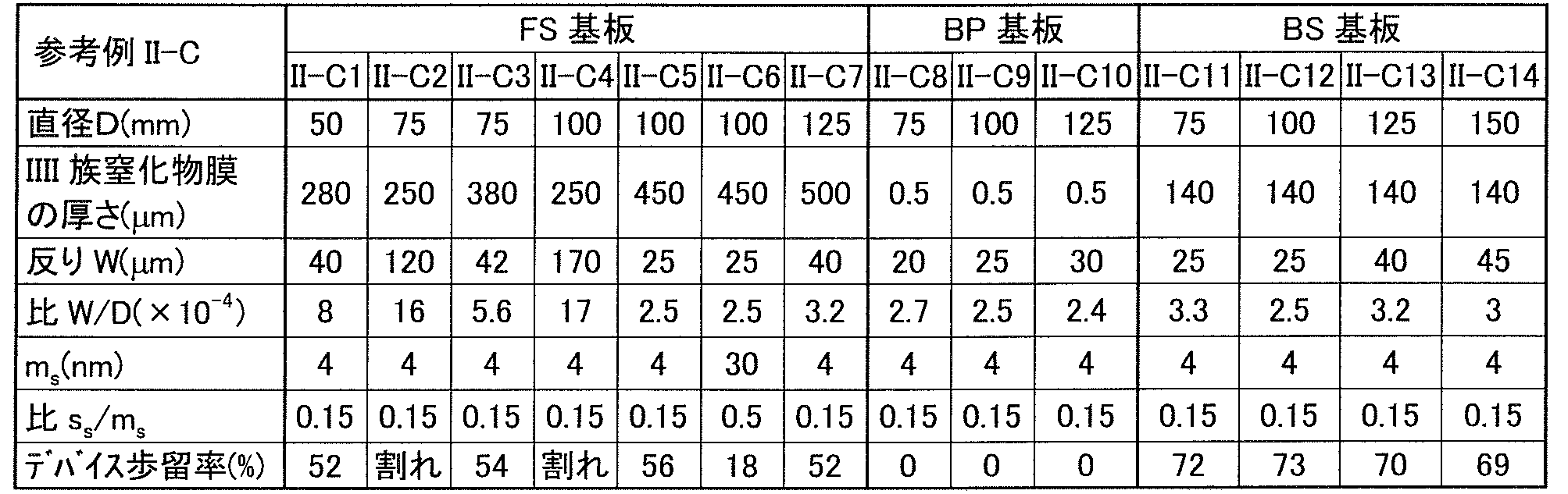
表14を参照して、直径50mm~125mmで厚さ250μm~500μmのFS基板を用いて作製したIII族窒化物半導体デバイスは、直径が大きく厚さが小さいものは反りが大きくまた割れが発生しやすく、いずれも歩留率が60%に満たなかった。
また、直径が75mm~125mmでIII族窒化物膜の厚さが0.5μmのBP基板を用いて作製したIII族窒化物半導体デバイスは、III族窒化物膜の厚さが小さいため、良好なデバイス特性が発現せず、歩留率が低下した。
これらに対して、BS基板を用いて作製したIII族窒化物半導体デバイスは、歩留率が69%以上と高かった。BS基板は、BP基板に比べてIII族窒化物膜が厚く十分に電流が広がること、BP基板とは異なりイオン注入によるIII族窒化物膜の結晶品質の低下がないことにより、良好な特性が得られた。
(参考例II-D)
図12および図15を参照して、支持基板11としてAl2O3-SiO2複合酸化物基板(基板全体に対してAl2O3が82質量%でSiO2が18質量%である)基板を用いたこと、直径をそれぞれ75mm~150mmの間で変動させ、接合膜12であるSiO2膜をAP-CVD(常圧-化学気相堆積)法により成長させ、支持基板11側の主面11nの仕上げ研磨においては作用係数FEが8.5×10⁻¹⁷m2/sの条件で研磨したこと、仕上げ研磨後のIII族窒化物膜13の厚さをそれぞれ110μm~130μmの間で変動させた1III族窒化物複合基板1を作製したこと、以外は、参考例II-Aと同様にして、III族窒化物複合基板1およびIII族窒化物半導体デバイス4を作製した。支持基板11は、熱伝導率が5W・m-1・K-1で、ヤング率が230GPaであった。
図12および図15を参照して、支持基板11としてAl2O3-SiO2複合酸化物基板(基板全体に対してAl2O3が82質量%でSiO2が18質量%である)基板を用いたこと、直径をそれぞれ75mm~150mmの間で変動させ、接合膜12であるSiO2膜をAP-CVD(常圧-化学気相堆積)法により成長させ、支持基板11側の主面11nの仕上げ研磨においては作用係数FEが8.5×10⁻¹⁷m2/sの条件で研磨したこと、仕上げ研磨後のIII族窒化物膜13の厚さをそれぞれ110μm~130μmの間で変動させた1III族窒化物複合基板1を作製したこと、以外は、参考例II-Aと同様にして、III族窒化物複合基板1およびIII族窒化物半導体デバイス4を作製した。支持基板11は、熱伝導率が5W・m-1・K-1で、ヤング率が230GPaであった。
参考例II-Aと同様にして、III族窒化物複合基板1について、支持基板11側の主面11nのRMSの平均値mS、支持基板11側の主面11nのRMSの平均値mSに対するRMSの標準偏差sSの比sS/mS、支持基板11側の主面11nの反りW、および直径Dに対する支持基板11側の主面11nの反りWの比W/Dを算出して、表15にまとめた。また、参考例II-Aと同様にして、III族窒化物半導体デバイス4の歩留率を算出して、表15にまとめた。

表15を参照して、厚さ110μm~130μm(この値は10μm以上250μm以下)のIII族窒化物膜を有する直径75mm~150mm(この値は75mm以上)のIII族窒化物複合基板であって、支持基板側の主面のRMSの平均値mSが3nm(この値は0.3nm以上20nm以下)であり、支持基板側の主面のRMSの平均値mSに対するRMSの標準偏差sSの比sS/mSが0.1(この値は0.005以上0.4以下)であり、直径Dに対する支持基板11側の主面11nの反りWの比W/Dが-7×10-4以上8×10-4以下であるIII族窒化物複合基板を用いて作製されたIII族窒化物半導体デバイスの歩留が高かった。
(参考例II-E)
図12および図15を参照して、支持基板11としてムライト基板(ムライト基板全体に対してAl2O3が60モル%でSiO2が40モル%である)を用いたこと、III族窒化物膜ドナー基板13DとしてO(酸素)原子およびSi(ケイ素)原子がドーピングされ転位集中領域がなく転位密度が5×106cm-2で均一でありキャリア濃度が2×1018cm-3の導電性が高いGaN基板を用いたこと、支持基板11側の主面11nの仕上げ研磨においては作用係数FEが8.3×10⁻¹⁷m2/sの条件で研磨したこと、III族窒化物膜ドナー基板13Dの切断を放電ワイヤー加工で実施したこと、III族窒化物膜13側の主面13mの仕上げ研磨の際に粒径が20nm~400nmのコロイダルシリカを含むスラリーを用いて作用係数FEを4×10-14以上1×10-13以下としたこと、以外は、参考例II-Aと同様にして、III族窒化物複合基板1およびIII族窒化物半導体デバイス4を作製した。支持基板11は、熱伝導率が3W・m-1・K-1で、ヤング率が200GPaであった。
図12および図15を参照して、支持基板11としてムライト基板(ムライト基板全体に対してAl2O3が60モル%でSiO2が40モル%である)を用いたこと、III族窒化物膜ドナー基板13DとしてO(酸素)原子およびSi(ケイ素)原子がドーピングされ転位集中領域がなく転位密度が5×106cm-2で均一でありキャリア濃度が2×1018cm-3の導電性が高いGaN基板を用いたこと、支持基板11側の主面11nの仕上げ研磨においては作用係数FEが8.3×10⁻¹⁷m2/sの条件で研磨したこと、III族窒化物膜ドナー基板13Dの切断を放電ワイヤー加工で実施したこと、III族窒化物膜13側の主面13mの仕上げ研磨の際に粒径が20nm~400nmのコロイダルシリカを含むスラリーを用いて作用係数FEを4×10-14以上1×10-13以下としたこと、以外は、参考例II-Aと同様にして、III族窒化物複合基板1およびIII族窒化物半導体デバイス4を作製した。支持基板11は、熱伝導率が3W・m-1・K-1で、ヤング率が200GPaであった。
参考例II-Aと同様にして、仕上げ研磨後のIII族窒化物複合基板1について、支持基板11側の主面11nのRMSの平均値mS、支持基板11側の主面11nのRMSの平均値mSに対するRMSの標準偏差sSの比sS/mSを算出して、表16にまとめた。
また、仕上げ研磨後のIII族窒化物複合基板1について、III族窒化物膜13側の主面13mのRMSの平均値mIII-N、III族窒化物膜13側の主面13mのRMSの平均値mIII-Nに対するRMSの標準偏差sIII-Nの比sIII-N/mIII-Nを表16にまとめた。ここで、RMSの平均値mIII-NおよびRMSの平均値mIII-Nに対するRMSの標準偏差sIII-Nの比sIII-N/mIII-Nは、図7に示すIII族窒化物膜13側の主面13m上において、1つの中心点PCと、その中心点PCから互いに直角な4方向上でかつ外縁から5mm内側にある4つの外側点POと、1つの中心点PCと4つの外側点POとの中間に位置する4つの点および4つの外側点の互いの中間に位置する4つの点をあわせた8つの中間点PMとで構成される13点の測定点PにおけるIII族窒化物膜13側の主面13mのRMSから算出した。
さらに、参考例II-Aと同様にして、III族窒化物半導体デバイス4の歩留率を算出して、表16にまとめた。
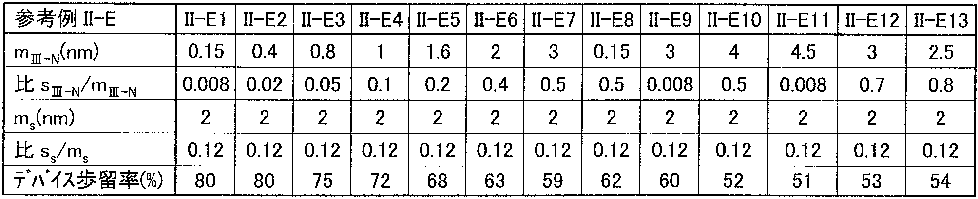
表16を参照して、厚さ110μm(この値は10μm以上250μm以下)のIII族窒化物膜を有する直径75mm(この値は75mm以上)のIII族窒化物複合基板であって、支持基板側の主面のRMSの平均値mSが2nm(この値は0.3nm以上20nm以下)であり、支持基板側の主面のRMSの平均値mSに対するRMSの標準偏差sSの比sS/mSが0.12(この値は0.005以上0.4以下)であり、III族窒化物膜側の主面のRMSの平均値mIII-Nが0.15nm以上3nm以下であり、III族窒化物膜側の主面のRMSの平均値mIII-Nに対する標準偏差sIII-Nの比sIII-N/mIII-Nが0.008以上0.5以下であるIII族窒化物複合基板を用いて作製されたIII族窒化物半導体デバイスの歩留が高かった。
(参考例II-F)
1.III族窒化物複合基板の作製
図12を参照して、支持基板11として、Al2O3-SiO2複合酸化物基板、ムライト基板(基板全体に対してAl2O3が60モル%でSiO2が40モル%である)、ムライト-YSZ基板(基板全体に対してムライトが70質量%でYSZが30質量%であり、ムライトに対してAl2O3が60モル%でSiO2が40モル%であり、YSZに対してZrO2が90モル%でY2O3が10モル%である)を用いたこと、III族窒化物膜ドナー基板13DとしてFe(鉄)原子をドーピングした電気抵抗率(比抵抗ともいう。)が2×10⁵Ωcmの半絶縁性のGaN基板を用いたこと、III族窒化物膜ドナー基板の切断を遊離砥粒を用いたワイヤーソーで実施したこと、支持基板11側の主面11nの仕上げ研磨においては作用係数FEが8.7×10⁻¹⁷m2/sの条件で研磨したこと、直径をそれぞれ75mm~150mmの間で変動させたIII族窒化物複合基板を作製したこと以外は、参考例II-Aと同様にして、III族窒化物複合基板1を作製した。
2.III族窒化物半導体デバイスの作製
図10を参照して、本参考例においては、III族窒化物半導体デバイス4として、HEMTを作製した。III族窒化物複合基板1のIII族窒化物膜13の主面13m上に、MOVPE法により、III族窒化物層20として、厚さ1.5μmのGaN層26、厚さ30nmのAl0.2Ga0.8N層27を順にエピタキシャル成長させることにより、積層III族窒化物複合基板2を得た。
図10を参照して、本参考例においては、III族窒化物半導体デバイス4として、HEMTを作製した。III族窒化物複合基板1のIII族窒化物膜13の主面13m上に、MOVPE法により、III族窒化物層20として、厚さ1.5μmのGaN層26、厚さ30nmのAl0.2Ga0.8N層27を順にエピタキシャル成長させることにより、積層III族窒化物複合基板2を得た。
次に、Al0.2Ga0.8N層27上にフォトリソグラフィ、EB蒸着、およびリフトオフによって、ソース電極60およびドレイン電極70を形成した。これらの電極の形成は、厚さ20nmのTi層、厚さ100nmのAl層、厚さ20nmのTi層、および厚さ300nmのAu層を順次形成し、リフトオフした後、600℃で1分間アニールすることにより合金化することにより行なった。
次に、ソース電極60およびドレイン電極70の形成と同様の工程により、ゲート電極80を形成した。ゲート電極80の形成は、厚さ50nmNi層および厚さ500nmのAu層を順次形成することにより行なった。ゲート長は2μmとした。
こうして得られたIII族窒化物半導体デバイス4であるHEMTは、III族窒化物複合基板1のIII族窒化物膜13上に、少なくとも1層の1層のIII族窒化物層20としてGaN層26およびAl0.2Ga0.8N層27が形成され、Al0.2Ga0.8N層27上にソース電極60、ドレイン電極70、およびゲート電極80が、お互いに分離され、かつ、ゲート電極80がソース電極60とドレイン電極70との間に位置するように、配置されていた。
参考例II-Aと同様にして、III族窒化物複合基板1について、支持基板11側の主面11nのRMSの平均値mS、支持基板11側の主面11nのRMSの平均値mSに対するRMSの標準偏差sSの比sS/mSを算出して、表17にまとめた。さらに、支持基板11の熱膨張係数αSおよびIII族窒化物膜13の熱膨張係数αIII-Nを熱機械分析装置により測定し、支持基板の熱膨張係数αSに対するIII族窒化物膜の熱膨張係数αIII-Nの比αIII-N/αSを算出して、結果を表17にまとめた。さらに、支持基板11の厚さtSおよびIII族窒化物膜13の厚さtIII-Nを、デジタルインジケーターにより測定し、支持基板11の厚さtSに対するIII族窒化物膜13の厚さtIII-Nの比tIII-N/tSを算出して、結果を表17にまとめた。
また、以下のようにして、III族窒化物半導体デバイス4の歩留率を算出した。すなわち、III族窒化物半導体デバイス4であるHEMTに5Vのゲート電圧を与えたときに、そのHEMTからリークしたゲート電流密度が1×10⁻⁶A/cm2以下の基準に適合したものを良品、適合しなかったものを不良品とし、良品を良品と不良品の合計で除したものの百分率を歩留率とした。

表17を参照して、III族窒化物複合基板であれば、支持基板11としてAl2O3-SiO2複合酸化物基板、ムライト基板、およびムライト-YSZ基板のいずれかを有するIII族窒化物複合基板1を用いても、そのIII族窒化物膜の厚さが110μm(この値は10μm~250μm)とし、直径が75mm~150mmであり、支持基板側の主面のRMSの平均値mSが1.5nm(この値は0.3nm以上20nm以下)であり、支持基板側の主面のRMSの平均値mSに対するRMSの標準偏差sSの比sS/mSが0.1(この値は0.005以上0.4以下)であるIII族窒化物複合基板1を用いて作製されたIII族窒化物半導体デバイスの歩留が高かった。また、支持基板11の熱膨張係数αSに対するIII族窒化物膜13の熱膨張係数αIII-Nの比αIII-N/αSが0.75以上1.25以下である場合、支持基板11の厚さtSに対するIII族窒化物膜の厚さtIII-Nの比tIII-N/tSが0.02以上1以下である場合に、作製されたIII族窒化物半導体デバイスの歩留が高かった。
(参考例II-G)
図12を参照して、支持基板11としてAl2O3-SiO2複合酸化物基板(基板全体に対してAl2O3が88質量%でSiO2が12質量%である)基板を用いたこと、研削および作用係数FEが5.9×10⁻¹⁷m2/sの仕上げ研磨により支持基板11の厚さを250μmとしたこと、直径をそれぞれ75mm~150mmの間で変動させた1III族窒化物複合基板1を作製したこと、得られたIII族窒化物複合基板1をさらに洗浄したこと以外は、参考例II-Aと同様にして、III族窒化物複合基板1を作製した。ここで、支持基板11は、熱伝導率が15W・m-1・K-1で、ヤング率が270GPaであった。また、洗浄方法は、界面活性剤と純水とを用いたスクラブ洗浄、塩酸またはTMAH(水酸化テトラメチルアンモニウム)と純水とを用いた二流体洗浄、ならびに塩酸またはTMAHと純水とを用いたメガソニック洗浄を組み合わせることにより実施した。
図12を参照して、支持基板11としてAl2O3-SiO2複合酸化物基板(基板全体に対してAl2O3が88質量%でSiO2が12質量%である)基板を用いたこと、研削および作用係数FEが5.9×10⁻¹⁷m2/sの仕上げ研磨により支持基板11の厚さを250μmとしたこと、直径をそれぞれ75mm~150mmの間で変動させた1III族窒化物複合基板1を作製したこと、得られたIII族窒化物複合基板1をさらに洗浄したこと以外は、参考例II-Aと同様にして、III族窒化物複合基板1を作製した。ここで、支持基板11は、熱伝導率が15W・m-1・K-1で、ヤング率が270GPaであった。また、洗浄方法は、界面活性剤と純水とを用いたスクラブ洗浄、塩酸またはTMAH(水酸化テトラメチルアンモニウム)と純水とを用いた二流体洗浄、ならびに塩酸またはTMAHと純水とを用いたメガソニック洗浄を組み合わせることにより実施した。
2.III族窒化物半導体デバイスの作製
図11を参照して、本参考例においては、III族窒化物半導体デバイス4として、SBDを作製した。図6に示すIII族窒化物複合基板1のIII族窒化物膜13の主面13m上に、MOVPE法により、III族窒化物層20として、厚さ2μmのn+-GaN層28(キャリア濃度が2×1018cm-3)、厚さ7μmのn--GaN層29(キャリア濃度が5×1015cm-3)を順にエピタキシャル成長させることにより、積層III族窒化物複合基板を得た。
図11を参照して、本参考例においては、III族窒化物半導体デバイス4として、SBDを作製した。図6に示すIII族窒化物複合基板1のIII族窒化物膜13の主面13m上に、MOVPE法により、III族窒化物層20として、厚さ2μmのn+-GaN層28(キャリア濃度が2×1018cm-3)、厚さ7μmのn--GaN層29(キャリア濃度が5×1015cm-3)を順にエピタキシャル成長させることにより、積層III族窒化物複合基板を得た。
次に、n--GaN層29上にEB(電子線)蒸着法により、厚さ4nmのNi層および厚さ200nmのAu層を順次形成し、アニールにより合金化することによりショットキー電極である第1電極30を形成した。電極径は200μmとした。第1電極30上に、EB蒸着法により、厚さ200nmのTi層、厚さ100nmのPt層、および厚さ1000nmのAu層を順次形成することによりパッド電極(図示せず)を形成した。
積層III族窒化物複合基板から支持基板および接合膜を研削により除去した。研削には平均粒径が40μm~50μmのダイヤモンド砥粒を用いたビトリファイド砥石を用いた。
図11を参照して、積層III族窒化物基板から支持基板および接合膜が除去された露出したIII族窒化物膜13の主面13n上に、EB蒸着法により、厚さ20nmのTi層、厚さ200nmのAl層、および厚さ300nmのAu層を順次形成し、アニールすることにより、オーミック電極である第2電極50を形成した。こうして、SBDとしてのIII族窒化物半導体デバイス4が得られた。
参考例II-Aと同様にして、III族窒化物複合基板1について、支持基板11側の主面11nのRMSの平均値mSを算出して、表18にまとめた。さらに、III族窒化物複合基板1について、III族窒化物膜13側の主面13mにおける不純物金属原子の濃度を、TXRF(全反射蛍光X分析)法により測定して、表18にまとめた。ここで、TXRF法による測定は、W(タングステン)線源を用いて、0.05°の入射角で行なった。
また、以下のようにして、III族窒化物半導体デバイス4の歩留率を算出した。すなわち、III族窒化物半導体デバイス4であるSBDについて逆方向の電流―電圧特性を測定し、そのSBDの耐圧が300V以上の基準に適合したものを良品、適合しなかったものを不良品とし、良品を表品と不良品との合計で除したものの百分率を歩留率とした。III族窒化物半導体デバイスの歩留率を表18にまとめた。

表18を参照して、厚さ110μmのIII族窒化物膜を有する直径75mm(この値は75mm以上)のIII族窒化物複合基板であって、III族窒化物膜側の主面における不純物金属原子の濃度が3×10¹²原子/cm2以下であるIII族窒化物複合基板を用いて作製されたIII族窒化物半導体デバイスの歩留が高かった。
(参考例II-H)
図14および図15を参照して、支持基板11として熱伝導率が2W・m-1・K-1~300W・m-1・K-1の間にある直径75mmの基板を用いたこと、直径75mmのIII族窒化物膜ドナー基板13Dの貼り合わせ主面と反対側の主面13mから研削および研磨を行なってIII族窒化物膜13の厚さを110μmとしたこと、支持基板11側の主面11nの仕上げ研磨においては作用係数FEが9.0×10⁻¹⁷m2/sの条件で研磨したこと、以外は、参考例II-Aと同様にして、III族窒化物複合基板1およびIII族窒化物半導体デバイス4を作製した。ここで、III族窒化物膜ドナー基板13Dの研削には、平均砥粒が25μm~35μmのダイヤモンド砥粒を含むビトリファイド砥粒を用いた。また、支持基板11の熱伝導率は、酸化物原料の配合比率、および焼成条件を調整することにより行なった。
図14および図15を参照して、支持基板11として熱伝導率が2W・m-1・K-1~300W・m-1・K-1の間にある直径75mmの基板を用いたこと、直径75mmのIII族窒化物膜ドナー基板13Dの貼り合わせ主面と反対側の主面13mから研削および研磨を行なってIII族窒化物膜13の厚さを110μmとしたこと、支持基板11側の主面11nの仕上げ研磨においては作用係数FEが9.0×10⁻¹⁷m2/sの条件で研磨したこと、以外は、参考例II-Aと同様にして、III族窒化物複合基板1およびIII族窒化物半導体デバイス4を作製した。ここで、III族窒化物膜ドナー基板13Dの研削には、平均砥粒が25μm~35μmのダイヤモンド砥粒を含むビトリファイド砥粒を用いた。また、支持基板11の熱伝導率は、酸化物原料の配合比率、および焼成条件を調整することにより行なった。
参考例II-Aと同様にして、III族窒化物半導体デバイス4の歩留率を算出して、表19にまとめた。

表19を参照して、厚さ110μm(この値は10μm以上250μm以下)のIII族窒化物膜を有する直径75mm(この値は75mm以上)のIII族窒化物複合基板であって、熱伝導率が3W・m-1・K-1以上280W・m-1・K-1以下である支持基板を有するIII族窒化物複合基板を用いて作製されたIII族窒化物半導体デバイスの歩留が高かった。
参考発明IIIにかかる参考例III-A~参考例III-Dについて以下に示す。
[(1) III族窒化物複合基板の作製]
(参考例III-A)
以下、図12を参照して、参考例に係るIII族窒化物複合基板を説明する。
[(1) III族窒化物複合基板の作製]
(参考例III-A)
以下、図12を参照して、参考例に係るIII族窒化物複合基板を説明する。
まず、図12(A)に示すように、支持基板11として直径75mmで厚さ300μmのAl2O3-SiO2複合酸化物基板(基板全体に対してAl2O3が85質量%であり、SiO2が15質量%である複合酸化物基板)を準備した。この支持基板11は、熱伝導率が10W・m-1・K-1であり、ヤング率が250GPaであった。
次いで、支持基板11の両側の主面11m,11nを、研磨剤としてダイヤモンドスラリーを用いて、銅系定盤により粗研磨、スズ系定盤により中間研磨、不織布研磨パッドにより仕上げ研磨を行なった。仕上げ研磨においては、作用係数FEが4×10-17m2/s以上1×10-16m2/s以下の条件で研磨した。
次に、支持基板11の仕上げ研磨後の主面11m上に、厚さ800nmのSiO2膜をPE-CVD(プラズマ援用-化学気相堆積)法により成長させ、窒素雰囲気中で800℃で1時間のアニールを行なった。
次に、平均粒径40nmのコロイダルシリカ砥粒を含みpHが10のスラリーを用いたCMPにより、主面12amがRMS(二乗平均平方根粗さ)で0.3nm以下に鏡面化された厚さ400nmの接合膜12aを形成した。次いで、CMPの際に用いたコロイダルシリカ砥粒を除去するために、KOH水溶液による無砥粒ポリシング洗浄、純水によるポリシング洗浄、および純水によるメガソニック洗浄(500kHz~5MHzのメガソニック帯域の周波数の超音波を用いた洗浄)を行なった。
また、図12(B)に示すように、III族窒化物膜ドナー基板13Dとして直径75mmで厚さ8mmのGaN結晶体を準備した。次いで、III族窒化物膜ドナー基板13Dの貼り合わせ面を機械研磨およびCMPによりRMSを2nm以下に平坦化し、その上に厚さ800nmのSiO2膜をPE-CVD法により成長させ、窒素雰囲気中、800℃で1時間のアニール行なった。続いて、平均粒径が40nmのコロイダルシリカ砥粒を含みpHが10のスラリーを用いたCMPにより、主面12bnがRMSで0.3nm以下に鏡面化された厚さ500nmの接合膜12bを形成した。次いで、CMPの際に用いたコロイダルシリカ砥粒を除去するために、KOH水溶液による無砥粒ポリシング洗浄、純水によるポリシング洗浄、および純水によるメガソニック洗浄を行なった。
なお、ここで、III族窒化物膜ドナー基板13Dは、下地基板としてGaAs基板を用いて、HVPE法により成長させたものであった。III族窒化物膜ドナー基板13Dは、n型の導電型であり、転移密度が1×108cm-2であり、キャリア濃度が1×1017cm-3であった。
次に、図12(C)に示すように、接合膜12aの主面12amと接合膜12bの主面12bnとを貼り合わせることにより、支持基板11とIII族窒化物膜13とを接合膜12を介在させて貼り合わせた接合基板1Lを得た。貼り合わせた後に、接合基板1Lを窒素雰囲気中で800℃まで昇温することによりアニールして接合強度を高めた。
次に、図12(D)に示すように、接合基板1LのIII族窒化物膜ドナー基板13Dを接合膜12との貼り合わせ面から内部に40μmの距離の深さに位置する面でワイヤーソーにより切断することによって、支持基板11とGaN薄膜であるIII族窒化物膜13とが接合膜12を介在させて貼り合わされたIII族窒化物複合基板1を得た。
なお、ここで、ワイヤーとしては、ダイヤモンド砥粒を電着させた線径180μmの固定砥粒ワイヤーを用いた。また、切断抵抗を低減して厚さの精度および切断面の平坦性を高めるために、切断方式としては、ワイヤーを揺動させ、それに同期してIII族窒化物膜ドナー基板13Dを振動させる方式を採用した。そして、ワイヤーソー切断の抵抗係数は4200Nとした。
さらに、切断後には、III族窒化物複合基板1のIII族窒化物膜13に対して機械研磨およびCMPを行なった。このとき、研磨材としてはダイヤモンドスラリーを用いて、銅系定盤により粗研磨、スズ系定盤により中間研磨を実施した。さらに、pH11のコロイダルシリカスラリー(平均粒径60nmのコロイダルシリカ砥粒を含みpH11のスラリー)を用いて、不織布研磨パッドにより仕上げ研磨を行なった。なお、III族窒化物膜13の厚さの均一化のため、CMPにおける複合基板の装置への取り付けには、予備的に真空チャック吸着によって基板形状を矯正した後に、該基板を装置に吸着固定する方式を採用した。また、仕上げ研磨の際の作用係数FEは7×10-14m2/sとした。仕上げ研磨後のIII族窒化物膜13の厚さは110μmであった。
[(2) III族窒化物半導体デバイスの作製]
以下、図16を参照して、参考例に係るIII族窒化物半導体デバイスであるSBD(ショットキーバリアダイオード)を説明する。
以下、図16を参照して、参考例に係るIII族窒化物半導体デバイスであるSBD(ショットキーバリアダイオード)を説明する。
まず、図16(A)に示すように、III族窒化物複合基板1のIII族窒化物膜13側の主面13m上に、MOVPE法により、III族窒化物層20として、厚さ2μmのn+-GaN層28(キャリア濃度が2×1018cm-3)、厚さ7μmのn--GaN層29(キャリア濃度が5×1015cm-3)を、この順序でエピタキシャル成長させることにより、積層III族窒化物複合基板2を得た。
次に、図16(B)に示すように、積層III族窒化物複合基板2のIII族窒化物層20の最上層であるn--GaN層29上に、電子線蒸着法(以下、EB(Electron Beam)蒸着法とも記す)により、厚さ4nmのNi層と厚さ200nmのAu層とを順次形成し、アニールにより合金化することによってショットキー電極である第1電極30を形成した。なお、このとき、第1電極30の径は200μmとした。さらに、第1電極30上に、EB蒸着法により、厚さ200nmのTi層と、厚さ100nmのPt層と、厚さ1000nmのAu層とを順次形成することによりパッド電極33を形成した。
また、デバイス支持基板40としてMo基板を準備し、デバイス支持基板40上にEB蒸着法により、厚さ200nmのTi層と、厚さ100nmのPt層と、厚さ1000nmのAu層とを順次形成することによりパッド電極43を形成した。そして、パッド電極43上に、接合金属膜44として、AuSnはんだ膜を形成した。
次に、パッド電極33に接合金属膜44を貼り合わせることにより、積層基板3を得た。
次に、図16(C)に示すように、積層基板3から、III族窒化物複合基板1の支持基板11および接合膜12を、フッ化水素酸を用いたエッチングにより除去した。
次に、図16(D)に示すように、積層基板3から支持基板11および接合膜12が除去されることによって露出したIII族窒化物膜13上に、EB蒸着法により、厚さ20nmのTi層と、厚さ200nmのAl層と、厚さ300nmのAu層とを順次形成し、アニールすることにより、オーミック電極である第2電極50を形成した。また、デバイス支持基板40上に、EB蒸着により、厚さ20nmのTi層と、厚さ300nmのAu層とを順次形成し、アニールすることにより、デバイス支持基板電極45を形成した。こうして、SBDであるIII族窒化物半導体デバイス4が得られた。
以上のようにして得られたIII族窒化物半導体デバイス4の歩留率は、以下のようにして算出した。すなわち、SBDについて逆方向の電流-電圧特性を測定し、耐電圧が250V以上の基準に適合したものを良品とし、適合しなかったものを不良品として、良品数を、良品数と不良品数との合計で除した値の百分率を歩留率とした。
以上に説明した方法により、表1に示す厚さ分布を有する接合膜を含むIII族窒化物複合基板、および、それらを用いたIII族窒化物半導体デバイスを作製した。
これらのIII族窒化物複合基板は、支持基板と、厚さが110μm(すなわち、10μm以上250μm以下)のIII族窒化物膜と、が貼り合わされた直径が75mm(すなわち、75mm以上)の複合基板であった。
接合膜の厚さ分布と、前述の方法により算出したIII族窒化物半導体デバイスの歩留率との関係を表20に示した。

表20より明らかなように、接合膜の厚さ分布が2%以上40%以下であるIII族窒化物複合基板を用いた半導体デバイス(III-A2~III-A6)は、かかる条件を満たさないIII族窒化物複合基板を用いた半導体デバイス(III-A1およびIII-A7)に比べて、歩留率が良好であった。
(参考例III-B)
参考例III-Aと同様にして、表21に示すせん断接合強度および接合面積率で、支持基板とIII族窒化物膜とが接合されたIII族窒化物複合基板、および、それらを用いたIII族窒化物半導体デバイスを作製した。
参考例III-Aと同様にして、表21に示すせん断接合強度および接合面積率で、支持基板とIII族窒化物膜とが接合されたIII族窒化物複合基板、および、それらを用いたIII族窒化物半導体デバイスを作製した。
これらのIII族窒化物複合基板は、支持基板と、厚さが110μm(すなわち、10μm以上250μm以下)のIII族窒化物膜と、が貼り合わされた直径が75mm(すなわち、75mm以上)の複合基板である。
せん断接合強度および接合面積率と、前述の方法により算出したIII族窒化物半導体デバイスの歩留率との関係を表21に示す。
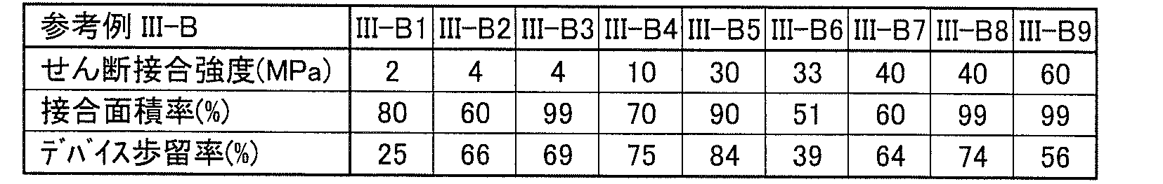
表21より明らかなように、支持基板とIII族窒化物膜とのせん断接合強度が4MPa以上40MPa以下であり、支持基板とIII族窒化物膜との接合面積率が60%以上99%以下であるIII族窒化物複合基板を用いた半導体デバイス(III-B2~III-B5、III-B7およびIII-B8)は、かかる条件を満たさないIII族窒化物複合基板を用いた半導体デバイス(III-B1、III-B6およびIII-B9)に比べて、歩留率が良好であった。
(参考例III-C)
以下の(i)~(v)以外の条件は、参考例III-Aと同様にして、参考例III-Cに係るIII族窒化物複合基板、および、それらを用いたIII族窒化物半導体デバイスを作製した。
(i)支持基板11として、Al2O3-SiO2複合酸化物基板(基板全体に対してAl2O3が82質量%であり、SiO2が18質量%である複合酸化物基板)、ムライト-YSZ、およびムライトから選択される複合酸化物基板を用いたこと
(ii)直径をそれぞれ75mm~150mmの間で変動させたこと
(iii)接合膜12をAP-CVD(常圧-化学気相堆積)法により成長させたこと
(iv)支持基板11側の主面11mの仕上げ研磨の際に作用係数FEが8.5×10⁻¹⁷m2/s以上1×10-16m2/s以下の条件で研磨したこと
(v)仕上げ研磨後のIII族窒化物膜13の厚さをそれぞれ10μm~250μmの間で変動させたこと
なお、参考例III-Cに係るIII族窒化物複合基板の接合膜の厚さ分布はすべて5%(すなわち、2%以上40%以下)とした。
参考例III-Cに係るIII族窒化物複合基板の構成と、それらを用いたIII族半導体デバイスの歩留率との関係を表22に示す。

表22中、αIII-N/αSは支持基板の熱膨張係数αSに対するIII族窒化物膜の熱膨張係数αIII-Nの比を示し、tIII-N/tSは支持基板の厚さtSに対するIII族窒化物膜の厚さtIII-Nの比を示している。
表22より明らかなように、支持基板と、厚さが10μm以上250μm以下のIII族窒化物膜と、が貼り合わされた直径が75mm以上のIII族窒化物複合基板であり、接合膜の厚さ分布が5%(すなわち、2%以上40%以下)であるIII族窒化物複合基板のうち、tIII-N/tSが0.02以上1以下である複合基板を用いたIII族窒化物半導体デバイスは特に高い歩留率で製造することができた。
上記に加えて、αIII-N/αSが0.75以上1.25以下である複合基板には、割れが全く発生しておらず、歩留まりも良好であった。
(参考例III-D)
表23に示す熱伝導率λsを有する支持基板を使用した以外は、参考例III-Aと同様にして、III族窒化物複合基板、および、それらを用いたIII族窒化物半導体デバイスを作製した。
表23に示す熱伝導率λsを有する支持基板を使用した以外は、参考例III-Aと同様にして、III族窒化物複合基板、および、それらを用いたIII族窒化物半導体デバイスを作製した。
支持基板の熱伝導率λsとIII族窒化物半導体デバイスの歩留率との関係を表23に示す。
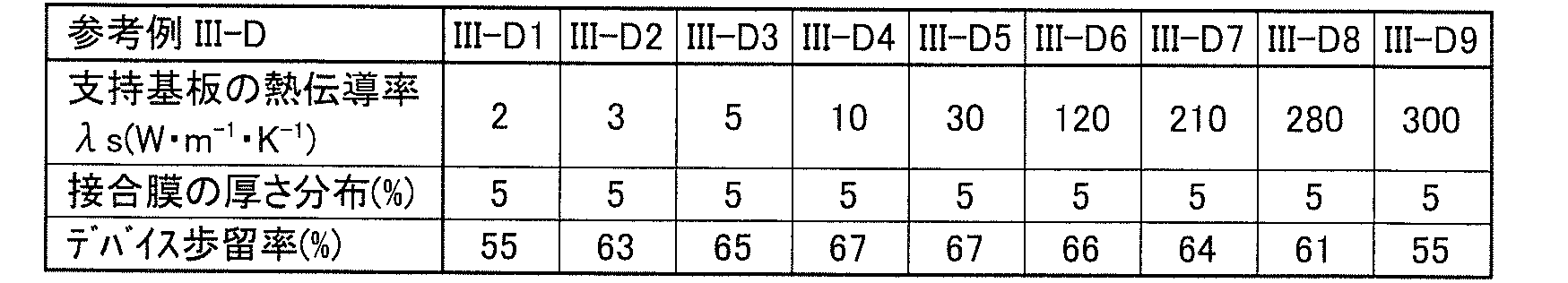
表23より明らかなように、支持基板と、厚さが110μm(すなわち、10μm以上250μm以下)のIII族窒化物膜と、が貼り合わされた直径が75mm(すなわち、75mm以上)のIII族窒化物複合基板であり、接合膜の厚さ分布が5%(すなわち、2%以上40%以下)であるIII族窒化物複合基板のうち、熱伝導率λSが3W・m-1・K-1以上280W・m-1・K-1以下である複合基板を用いたIII族窒化物半導体デバイスは特に高い歩留率で製造することができた。
今回開示された実施の形態および実施例はすべての点で例示であって制限的なものではないと考えられるべきである。本発明の範囲は上記した説明ではなくて請求の範囲によって示され、請求の範囲と均等の意味および範囲内でのすべての変更が含まれることが意図される。
1 III族窒化物複合基板、1L,1LS 接合基板、2 積層III族窒化物複合基板、3 積層基板、4 III族窒化物半導体デバイス、5D,5Dr 支持体付III族窒化物膜ドナー基板、11 支持基板、11m,11n,12am,12bn,13m,13n 主面、12,12a,12b,14 接合膜、13 III族窒化物膜、13D,13Dr III族窒化物膜ドナー基板、13h 主面貫通孔、13i イオン注入領域、15 III族窒化物膜ドナー基板支持体、20 III族窒化物層、21 n-GaN層、22 n-In0.05Ga0.95N層、23 活性層、24 p-Al0.09Ga0.91N層、25 p-GaN層、26 GaN層、27 Al0.2Ga0.8N層、28 n+-GaN層、29 n--GaN層、30 第1電極、33,43 パッド電極、40 デバイス支持基板、44 接合金属膜、45 デバイス支持基板電極、50 第2電極、60 ソース電極、70 ドレイン電極、80 ゲート電極、100 接合界面、100b 接合領域、100n 非接合領域、111n,112n,121n,122n 非接合部分領域、201 第1導電型GaN層、202 第1導電型AlsGa1-sN層、203 発光層、204 第2導電型AltGa1-tN層、205 第2導電型GaN層。
Claims (10)
- III族窒化物膜と、前記III族窒化物膜と化学組成の異なる材料で形成されている支持基板と、を含み、
前記III族窒化物膜は、前記支持基板に直接的および間接的のいずれかの形態で接合され、
前記III族窒化物膜の厚さが10μm以上であり、
前記III族窒化物膜側の主面におけるシート抵抗が200Ω/sq以下であるIII族窒化物複合基板。 - 前記III族窒化物膜と前記支持基板との接合領域の面積が主面の面積の70%以上であり、
前記III族窒化物膜と前記支持基板との非接合領域は少なくとも1つの非接合部分領域を含み、前記非接合部分領域はその最大径が20mm未満の小型の非接合部分領域である請求項1に記載のIII族窒化物複合基板。 - [規則91に基づく訂正 09.01.2014]
前記III族窒化物膜と前記支持基板との非接合領域は少なくとも1つの非接合部分領域を含み、前記非接合部分領域は主面の外周に接していない内側の非接合部分領域である請求項1に記載のIII族窒化物複合基板。 - 前記III族窒化物膜は主面貫通孔を有し、前記主面貫通孔の面積は主面の面積の10%以下である請求項1に記載のIII族窒化物複合基板。
- 前記III族窒化物膜と前記支持基板との接合界面に金属を含む不純物を含み、前記不純物の濃度が1×1010cm-2以上である請求項1に記載のIII族窒化物複合基板。
- 前記III族窒化物膜の熱膨張係数が前記支持基板の熱膨張係数に比べて0.7倍より大きく1.4倍より小さい請求項1に記載のIII族窒化物複合基板。
- 前記支持基板の破壊靭性が1MNm-2/3以上であり、前記支持基板の厚さが50μm以上である請求項1に記載のIII族窒化物複合基板。
- 前記間接的な形態は、前記III族窒化物膜と前記支持基板との間に接合膜を介在させた形態である請求項1に記載のIII族窒化物複合基板。
- 請求項1に記載のIII族窒化物複合基板の製造方法であって、
前記III族窒化物膜と前記支持基板とを、直接的および間接的のいずれかの形態で、貼り合わせる工程と、
貼り合わされた前記III族窒化物膜および前記支持基板の少なくとも1つの厚さを小さくする工程と、を含むIII族窒化物複合基板の製造方法。 - 請求項1に記載のIII族窒化物複合基板を用いたIII族窒化物半導体デバイスの製造方法であって、
前記III族窒化物複合基板を準備する工程と、
前記III族窒化物複合基板の前記III族窒化物膜側の主面上に少なくとも1層のIII族窒化物層を成長させる工程と、を含むIII族窒化物半導体デバイスの製造方法。
Priority Applications (6)
| Application Number | Priority Date | Filing Date | Title |
|---|---|---|---|
| EP13845267.7A EP2908330B1 (en) | 2012-10-12 | 2013-09-04 | Group iii nitride composite substrate, manufacturing method therefor, and group iii nitride semiconductor device manufacturing method |
| CN201380046378.9A CN104641453B (zh) | 2012-10-12 | 2013-09-04 | Iii族氮化物复合衬底及其制造方法以及制造iii族氮化物半导体器件的方法 |
| CN201810174097.6A CN108281378B (zh) | 2012-10-12 | 2013-09-04 | Iii族氮化物复合衬底、半导体器件及它们的制造方法 |
| US14/419,315 US9917004B2 (en) | 2012-10-12 | 2013-09-04 | Group III nitride composite substrate and method for manufacturing the same, and method for manufacturing group III nitride semiconductor device |
| US15/879,018 US10600676B2 (en) | 2012-10-12 | 2018-01-24 | Group III nitride composite substrate and method for manufacturing the same, and method for manufacturing group III nitride semiconductor device |
| US16/787,700 US11094537B2 (en) | 2012-10-12 | 2020-02-11 | Group III nitride composite substrate and method for manufacturing the same, and method for manufacturing group III nitride semiconductor device |
Applications Claiming Priority (16)
| Application Number | Priority Date | Filing Date | Title |
|---|---|---|---|
| US201261712967P | 2012-10-12 | 2012-10-12 | |
| JP2012226777 | 2012-10-12 | ||
| JP2012-226777 | 2012-10-12 | ||
| US61/712,967 | 2012-10-12 | ||
| JP2012-263090 | 2012-11-30 | ||
| JP2012263090 | 2012-11-30 | ||
| US201361762407P | 2013-02-08 | 2013-02-08 | |
| US61/762,407 | 2013-02-08 | ||
| JP2013029114A JP6248395B2 (ja) | 2013-02-18 | 2013-02-18 | Iii族窒化物複合基板およびその製造方法、積層iii族窒化物複合基板、ならびにiii族窒化物半導体デバイスおよびその製造方法 |
| JP2013-029114 | 2013-02-18 | ||
| JP2013029115A JP6322890B2 (ja) | 2013-02-18 | 2013-02-18 | Iii族窒化物複合基板およびその製造方法、ならびにiii族窒化物半導体デバイスの製造方法 |
| JP2013-029115 | 2013-02-18 | ||
| JP2013029125A JP6146042B2 (ja) | 2013-02-18 | 2013-02-18 | Iii族窒化物複合基板およびその製造方法、積層iii族窒化物複合基板、ならびにiii族窒化物半導体デバイスおよびその製造方法 |
| JP2013-029125 | 2013-02-18 | ||
| JP2013179839A JP6232853B2 (ja) | 2012-10-12 | 2013-08-30 | Iii族窒化物複合基板およびその製造方法、積層iii族窒化物複合基板、ならびにiii族窒化物半導体デバイスおよびその製造方法 |
| JP2013-179839 | 2013-08-30 |
Related Child Applications (2)
| Application Number | Title | Priority Date | Filing Date |
|---|---|---|---|
| US14/419,315 A-371-Of-International US9917004B2 (en) | 2012-10-12 | 2013-09-04 | Group III nitride composite substrate and method for manufacturing the same, and method for manufacturing group III nitride semiconductor device |
| US15/879,018 Continuation US10600676B2 (en) | 2012-10-12 | 2018-01-24 | Group III nitride composite substrate and method for manufacturing the same, and method for manufacturing group III nitride semiconductor device |
Publications (1)
| Publication Number | Publication Date |
|---|---|
| WO2014057748A1 true WO2014057748A1 (ja) | 2014-04-17 |
Family
ID=53218596
Family Applications (1)
| Application Number | Title | Priority Date | Filing Date |
|---|---|---|---|
| PCT/JP2013/073805 Ceased WO2014057748A1 (ja) | 2012-10-12 | 2013-09-04 | Iii族窒化物複合基板およびその製造方法、ならびにiii族窒化物半導体デバイスの製造方法 |
Country Status (5)
| Country | Link |
|---|---|
| US (3) | US9917004B2 (ja) |
| EP (1) | EP2908330B1 (ja) |
| CN (2) | CN108281378B (ja) |
| TW (2) | TWI646635B (ja) |
| WO (1) | WO2014057748A1 (ja) |
Cited By (3)
| Publication number | Priority date | Publication date | Assignee | Title |
|---|---|---|---|---|
| US20160351750A1 (en) * | 2014-05-21 | 2016-12-01 | Xiamen Sanan Optoelectronics Technology Co., Ltd. | Fabrication Method of Nitride Light Emitting Diodes |
| CN106415846A (zh) * | 2014-06-13 | 2017-02-15 | 英特尔公司 | 通过层转移在反向极化衬底上的高电子迁移率晶体管制造工艺 |
| CN115398605A (zh) * | 2020-04-14 | 2022-11-25 | 株式会社田村制作所 | 半导体膜及其制造方法 |
Families Citing this family (20)
| Publication number | Priority date | Publication date | Assignee | Title |
|---|---|---|---|---|
| JP6322890B2 (ja) | 2013-02-18 | 2018-05-16 | 住友電気工業株式会社 | Iii族窒化物複合基板およびその製造方法、ならびにiii族窒化物半導体デバイスの製造方法 |
| CN108281378B (zh) | 2012-10-12 | 2022-06-24 | 住友电气工业株式会社 | Iii族氮化物复合衬底、半导体器件及它们的制造方法 |
| CN104995713A (zh) | 2013-02-18 | 2015-10-21 | 住友电气工业株式会社 | Iii族氮化物复合衬底及其制造方法,层叠的iii族氮化物复合衬底,以及iii族氮化物半导体器件及其制造方法 |
| JP6606879B2 (ja) * | 2015-06-15 | 2019-11-20 | 富士電機株式会社 | 窒化物半導体装置の製造方法 |
| US9770688B2 (en) * | 2015-10-22 | 2017-09-26 | King Fahd University Of Petroleum And Minerals | Si—Y nanocomposite membrane and methods of making and use thereof |
| KR20170110500A (ko) * | 2016-03-22 | 2017-10-11 | 스미토모덴키고교가부시키가이샤 | 세라믹 기판, 적층체 및 saw 디바이스 |
| JP6662160B2 (ja) * | 2016-04-07 | 2020-03-11 | 住友電気工業株式会社 | 多結晶セラミック基板、接合層付き多結晶セラミック基板および積層基板 |
| CN109417020A (zh) * | 2016-04-12 | 2019-03-01 | 璐米斯塔尔有限公司 | 包括半绝缘氮化物半导体层的氮化物半导体基板的制造方法及利用该方法制造的氮化物半导体基板 |
| KR101914289B1 (ko) * | 2016-08-18 | 2018-11-01 | 주식회사 티씨케이 | 투과도가 다른 복수 개의 층을 갖는 SiC 반도체 제조용 부품 및 그 제조방법 |
| US10438792B2 (en) * | 2016-10-20 | 2019-10-08 | QROMIS, Inc. | Methods for integration of elemental and compound semiconductors on a ceramic substrate |
| JP6761322B2 (ja) * | 2016-10-21 | 2020-09-23 | 株式会社サイオクス | Iii族窒化物基板の製造方法およびiii族窒化物基板 |
| KR102680861B1 (ko) * | 2016-12-15 | 2024-07-03 | 삼성전자주식회사 | 질화 갈륨 기판의 제조 방법 |
| JP7039684B2 (ja) * | 2017-07-20 | 2022-03-22 | スウェガン、アクチボラグ | 高電子移動度トランジスタのためのヘテロ構造及びその製造方法 |
| JP6783990B2 (ja) * | 2017-09-07 | 2020-11-11 | 豊田合成株式会社 | Iii族窒化物半導体素子の製造方法および基板の製造方法 |
| JP6512369B1 (ja) * | 2017-09-21 | 2019-05-15 | 住友電気工業株式会社 | 半絶縁性化合物半導体基板および半絶縁性化合物半導体単結晶 |
| US11031167B2 (en) * | 2017-11-21 | 2021-06-08 | University Of New Hampshire | Giant perpendicular magnetic anisotropy in Fe/GaN thin films for data storage and memory devices |
| CN109508786B (zh) * | 2018-09-29 | 2022-04-08 | 南京邮电大学 | 一种学习、记忆和判决识别的光子类脑器件及其制备方法 |
| JP7262027B2 (ja) * | 2019-05-17 | 2023-04-21 | パナソニックIpマネジメント株式会社 | Iii族窒化物半導体の製造方法 |
| CN110718453B (zh) * | 2019-11-15 | 2021-08-20 | 武汉新芯集成电路制造有限公司 | 半导体器件及其制造方法 |
| FR3114909B1 (fr) * | 2020-10-06 | 2023-03-17 | Soitec Silicon On Insulator | Procédé de fabrication d’un substrat pour la croissance épitaxiale d’une couche d’un alliage III-N à base de gallium |
Citations (6)
| Publication number | Priority date | Publication date | Assignee | Title |
|---|---|---|---|---|
| JP2002319545A (ja) * | 2001-04-20 | 2002-10-31 | Mitsubishi Cable Ind Ltd | GaN系結晶の製造方法および結晶成長用基材 |
| JP2006210660A (ja) | 2005-01-28 | 2006-08-10 | Hitachi Cable Ltd | 半導体基板の製造方法 |
| JP2008010766A (ja) | 2006-06-30 | 2008-01-17 | Sumitomo Electric Ind Ltd | GaN薄膜貼り合わせ基板およびその製造方法、ならびにGaN系半導体デバイスおよびその製造方法 |
| JP2008166646A (ja) * | 2007-01-04 | 2008-07-17 | Covalent Materials Corp | 半導体基板の製造方法 |
| JP2009126722A (ja) | 2007-11-20 | 2009-06-11 | Sumitomo Electric Ind Ltd | Iii族窒化物半導体結晶基板および半導体デバイス |
| JP2010182936A (ja) | 2009-02-06 | 2010-08-19 | Sumitomo Electric Ind Ltd | 複合基板、エピタキシャル基板、半導体デバイス及び複合基板の製造方法 |
Family Cites Families (187)
| Publication number | Priority date | Publication date | Assignee | Title |
|---|---|---|---|---|
| US1960014A (en) | 1930-06-30 | 1934-05-22 | Johnston Edwin Lloyd | Float valve |
| JP3026087B2 (ja) * | 1989-03-01 | 2000-03-27 | 豊田合成株式会社 | 窒化ガリウム系化合物半導体の気相成長方法 |
| US5290393A (en) * | 1991-01-31 | 1994-03-01 | Nichia Kagaku Kogyo K.K. | Crystal growth method for gallium nitride-based compound semiconductor |
| US5406123A (en) * | 1992-06-11 | 1995-04-11 | Engineering Research Ctr., North Carolina State Univ. | Single crystal titanium nitride epitaxial on silicon |
| US5679152A (en) * | 1994-01-27 | 1997-10-21 | Advanced Technology Materials, Inc. | Method of making a single crystals Ga*N article |
| JPH09219540A (ja) * | 1996-02-07 | 1997-08-19 | Rikagaku Kenkyusho | GaN薄膜の形成方法 |
| JP3306578B2 (ja) * | 1996-10-24 | 2002-07-24 | 昭和電工株式会社 | 化合物半導体エピタキシャルウエハ |
| US5741724A (en) * | 1996-12-27 | 1998-04-21 | Motorola | Method of growing gallium nitride on a spinel substrate |
| US6091083A (en) * | 1997-06-02 | 2000-07-18 | Sharp Kabushiki Kaisha | Gallium nitride type compound semiconductor light-emitting device having buffer layer with non-flat surface |
| CA2311132C (en) * | 1997-10-30 | 2004-12-07 | Sumitomo Electric Industries, Ltd. | Gan single crystalline substrate and method of producing the same |
| US6194742B1 (en) * | 1998-06-05 | 2001-02-27 | Lumileds Lighting, U.S., Llc | Strain engineered and impurity controlled III-V nitride semiconductor films and optoelectronic devices |
| TW417315B (en) * | 1998-06-18 | 2001-01-01 | Sumitomo Electric Industries | GaN single crystal substrate and its manufacture method of the same |
| TW418549B (en) * | 1998-06-26 | 2001-01-11 | Sharp Kk | Crystal growth method for nitride semiconductor, nitride semiconductor light emitting device, and method for producing the same |
| US6713789B1 (en) * | 1999-03-31 | 2004-03-30 | Toyoda Gosei Co., Ltd. | Group III nitride compound semiconductor device and method of producing the same |
| US6563144B2 (en) * | 1999-09-01 | 2003-05-13 | The Regents Of The University Of California | Process for growing epitaxial gallium nitride and composite wafers |
| US6521514B1 (en) * | 1999-11-17 | 2003-02-18 | North Carolina State University | Pendeoepitaxial methods of fabricating gallium nitride semiconductor layers on sapphire substrates |
| JP4547746B2 (ja) * | 1999-12-01 | 2010-09-22 | ソニー株式会社 | 窒化物系iii−v族化合物の結晶製造方法 |
| FR2810159B1 (fr) * | 2000-06-09 | 2005-04-08 | Centre Nat Rech Scient | Couche epaisse de nitrure de gallium ou de nitrure mixte de gallium et d'un autre metal, procede de preparation, et dispositif electronique ou optoelectronique comprenant une telle couche |
| JP5145617B2 (ja) * | 2000-07-03 | 2013-02-20 | 日亜化学工業株式会社 | n型窒化物半導体積層体およびそれを用いる半導体素子 |
| EP1307903A1 (en) * | 2000-08-04 | 2003-05-07 | The Regents Of The University Of California | Method of controlling stress in gallium nitride films deposited on substrates |
| US6673149B1 (en) * | 2000-09-06 | 2004-01-06 | Matsushita Electric Industrial Co., Ltd | Production of low defect, crack-free epitaxial films on a thermally and/or lattice mismatched substrate |
| US6391748B1 (en) * | 2000-10-03 | 2002-05-21 | Texas Tech University | Method of epitaxial growth of high quality nitride layers on silicon substrates |
| JP2002222771A (ja) * | 2000-11-21 | 2002-08-09 | Ngk Insulators Ltd | Iii族窒化物膜の製造方法、iii族窒化物膜の製造用下地膜、及びその下地膜の製造方法 |
| US6649287B2 (en) * | 2000-12-14 | 2003-11-18 | Nitronex Corporation | Gallium nitride materials and methods |
| JP2002274996A (ja) * | 2001-01-15 | 2002-09-25 | Ngk Insulators Ltd | エピタキシャル下地基板及びエピタキシャル基板 |
| US6497763B2 (en) * | 2001-01-19 | 2002-12-24 | The United States Of America As Represented By The Secretary Of The Navy | Electronic device with composite substrate |
| AU2002306436A1 (en) * | 2001-02-12 | 2002-10-15 | Asm America, Inc. | Improved process for deposition of semiconductor films |
| JP2002343717A (ja) * | 2001-05-18 | 2002-11-29 | Matsushita Electric Ind Co Ltd | 半導体結晶の製造方法 |
| US6488767B1 (en) * | 2001-06-08 | 2002-12-03 | Advanced Technology Materials, Inc. | High surface quality GaN wafer and method of fabricating same |
| JP2003063897A (ja) * | 2001-08-28 | 2003-03-05 | Sony Corp | 窒化物系iii−v族化合物半導体基板およびその製造方法ならびに半導体発光素子の製造方法ならびに半導体装置の製造方法 |
| JP3856750B2 (ja) * | 2001-11-13 | 2006-12-13 | 松下電器産業株式会社 | 半導体装置及びその製造方法 |
| JP2003165798A (ja) | 2001-11-28 | 2003-06-10 | Hitachi Cable Ltd | 窒化ガリウム単結晶基板の製造方法、窒化ガリウム単結晶のエピタキシャル成長自立基板、及びその上に形成したデバイス素子 |
| JP2003197961A (ja) * | 2001-12-27 | 2003-07-11 | Toyoda Gosei Co Ltd | Iii族窒化物系化合物半導体発光素子 |
| JP3878868B2 (ja) * | 2002-03-01 | 2007-02-07 | シャープ株式会社 | GaN系レーザ素子 |
| US6812471B2 (en) | 2002-03-13 | 2004-11-02 | Applied Materials, Inc. | Method of surface texturizing |
| JP2003327497A (ja) * | 2002-05-13 | 2003-11-19 | Sumitomo Electric Ind Ltd | GaN単結晶基板、窒化物系半導体エピタキシャル基板、窒化物系半導体素子及びその製造方法 |
| KR100952015B1 (ko) * | 2002-12-10 | 2010-04-08 | 엘지이노텍 주식회사 | 반도체 소자 제조방법 |
| US7427555B2 (en) * | 2002-12-16 | 2008-09-23 | The Regents Of The University Of California | Growth of planar, non-polar gallium nitride by hydride vapor phase epitaxy |
| US20060169996A1 (en) * | 2002-12-27 | 2006-08-03 | General Electric Company | Crystalline composition, wafer, and semi-conductor structure |
| US7786503B2 (en) * | 2002-12-27 | 2010-08-31 | Momentive Performance Materials Inc. | Gallium nitride crystals and wafers and method of making |
| US6989314B2 (en) * | 2003-02-12 | 2006-01-24 | S.O.I.Tec Silicon On Insulator Technologies S.A. | Semiconductor structure and method of making same |
| JP2004247412A (ja) * | 2003-02-12 | 2004-09-02 | Yamaha Corp | 半導体積層構造及びその製造方法並びにそれを備えた半導体装置 |
| GB2398672A (en) * | 2003-02-19 | 2004-08-25 | Qinetiq Ltd | Group IIIA nitride buffer layers |
| KR20040078211A (ko) * | 2003-03-03 | 2004-09-10 | 엘지전자 주식회사 | 질화갈륨 기판 제조 방법 |
| JP4052150B2 (ja) * | 2003-03-05 | 2008-02-27 | 住友電気工業株式会社 | 窒化物系半導体装置の製造方法 |
| KR100550491B1 (ko) | 2003-05-06 | 2006-02-09 | 스미토모덴키고교가부시키가이샤 | 질화물 반도체 기판 및 질화물 반도체 기판의 가공 방법 |
| JP3760997B2 (ja) * | 2003-05-21 | 2006-03-29 | サンケン電気株式会社 | 半導体基体 |
| JP3913194B2 (ja) * | 2003-05-30 | 2007-05-09 | シャープ株式会社 | 窒化物半導体発光素子 |
| US7125801B2 (en) * | 2003-08-06 | 2006-10-24 | Matsushita Electric Industrial Co., Ltd. | Method of manufacturing Group III nitride crystal substrate, etchant used in the method, Group III nitride crystal substrate, and semiconductor device including the same |
| WO2005043604A2 (en) * | 2003-10-23 | 2005-05-12 | North Carolina State University | Growth and integration of epitaxial gallium nitride films with silicon-based devices |
| JP4380294B2 (ja) * | 2003-10-29 | 2009-12-09 | 日立電線株式会社 | Iii−v族窒化物系半導体基板 |
| US7276779B2 (en) * | 2003-11-04 | 2007-10-02 | Hitachi Cable, Ltd. | III-V group nitride system semiconductor substrate |
| US7323256B2 (en) * | 2003-11-13 | 2008-01-29 | Cree, Inc. | Large area, uniformly low dislocation density GaN substrate and process for making the same |
| US7118813B2 (en) * | 2003-11-14 | 2006-10-10 | Cree, Inc. | Vicinal gallium nitride substrate for high quality homoepitaxy |
| JP3894191B2 (ja) * | 2003-11-26 | 2007-03-14 | 住友電気工業株式会社 | 窒化ガリウム系半導体膜を形成する方法、および半導体基板生産物 |
| FR2864970B1 (fr) * | 2004-01-09 | 2006-03-03 | Soitec Silicon On Insulator | Substrat a support a coefficient de dilatation thermique determine |
| EP1709670B1 (en) * | 2004-01-26 | 2012-09-12 | Showa Denko K.K. | Group iii nitride semiconductor multilayer structure |
| JP5194334B2 (ja) * | 2004-05-18 | 2013-05-08 | 住友電気工業株式会社 | Iii族窒化物半導体デバイスの製造方法 |
| JP4622720B2 (ja) | 2004-07-21 | 2011-02-02 | 日亜化学工業株式会社 | 窒化物半導体ウエハ又は窒化物半導体素子の製造方法 |
| TW200610150A (en) * | 2004-08-30 | 2006-03-16 | Kyocera Corp | Sapphire baseplate, epitaxial substrate and semiconductor device |
| TWI375994B (en) * | 2004-09-01 | 2012-11-01 | Sumitomo Electric Industries | Epitaxial substrate and semiconductor element |
| US7633097B2 (en) * | 2004-09-23 | 2009-12-15 | Philips Lumileds Lighting Company, Llc | Growth of III-nitride light emitting devices on textured substrates |
| JP2006193348A (ja) * | 2005-01-11 | 2006-07-27 | Sumitomo Electric Ind Ltd | Iii族窒化物半導体基板およびその製造方法 |
| US20060175681A1 (en) * | 2005-02-08 | 2006-08-10 | Jing Li | Method to grow III-nitride materials using no buffer layer |
| WO2006087958A1 (ja) * | 2005-02-21 | 2006-08-24 | Mitsubishi Chemical Corporation | 窒化物半導体材料および窒化物半導体結晶の製造方法 |
| KR100631905B1 (ko) * | 2005-02-22 | 2006-10-11 | 삼성전기주식회사 | 질화물 단결정 기판 제조방법 및 이를 이용한 질화물 반도체 발광소자 제조방법 |
| JP4818732B2 (ja) * | 2005-03-18 | 2011-11-16 | シャープ株式会社 | 窒化物半導体素子の製造方法 |
| US7422634B2 (en) * | 2005-04-07 | 2008-09-09 | Cree, Inc. | Three inch silicon carbide wafer with low warp, bow, and TTV |
| JP2006290677A (ja) * | 2005-04-11 | 2006-10-26 | Hitachi Cable Ltd | 窒化物系化合物半導体結晶の製造方法及び窒化物系化合物半導体基板の製造方法 |
| KR100669142B1 (ko) * | 2005-04-20 | 2007-01-15 | (주)더리즈 | 발광 소자와 이의 제조 방법 |
| JP4432827B2 (ja) * | 2005-04-26 | 2010-03-17 | 住友電気工業株式会社 | Iii族窒化物半導体素子およびエピタキシャル基板 |
| JP4792802B2 (ja) * | 2005-04-26 | 2011-10-12 | 住友電気工業株式会社 | Iii族窒化物結晶の表面処理方法 |
| US7365374B2 (en) * | 2005-05-03 | 2008-04-29 | Nitronex Corporation | Gallium nitride material structures including substrates and methods associated with the same |
| JP5283502B2 (ja) * | 2005-05-11 | 2013-09-04 | ノース・キャロライナ・ステイト・ユニヴァーシティ | 極性が制御されたiii族窒化物薄膜及びその製法 |
| US20060267043A1 (en) * | 2005-05-27 | 2006-11-30 | Emerson David T | Deep ultraviolet light emitting devices and methods of fabricating deep ultraviolet light emitting devices |
| US7405430B2 (en) * | 2005-06-10 | 2008-07-29 | Cree, Inc. | Highly uniform group III nitride epitaxial layers on 100 millimeter diameter silicon carbide substrates |
| KR100638869B1 (ko) * | 2005-06-21 | 2006-10-27 | 삼성전기주식회사 | 질화물계 화합물층을 형성하는 방법 및 이를 이용한 GaN기판 및 수직구조 질화물계 반도체 발광소자를 제조하는방법 |
| FR2888402B1 (fr) * | 2005-07-06 | 2007-12-21 | Commissariat Energie Atomique | Procede d'assemblage de substrats par depot d'une couche mince de collage d'oxyde ou de nitrure et structure ainsi assemblee |
| JP2007059850A (ja) * | 2005-08-26 | 2007-03-08 | Ngk Insulators Ltd | Iii族窒化物成膜用基板及びその製造方法並びにそれを用いた半導体装置 |
| JP4529846B2 (ja) * | 2005-09-06 | 2010-08-25 | 日立電線株式会社 | Iii−v族窒化物系半導体基板及びその製造方法 |
| US8334155B2 (en) * | 2005-09-27 | 2012-12-18 | Philips Lumileds Lighting Company Llc | Substrate for growing a III-V light emitting device |
| JP4720441B2 (ja) | 2005-11-02 | 2011-07-13 | 日立電線株式会社 | 青色発光ダイオード用GaN基板 |
| US20070138505A1 (en) * | 2005-12-12 | 2007-06-21 | Kyma Technologies, Inc. | Low defect group III nitride films useful for electronic and optoelectronic devices and methods for making the same |
| JP2007242853A (ja) * | 2006-03-08 | 2007-09-20 | Sanken Electric Co Ltd | 半導体基体及びこれを使用した半導体装置 |
| JP2007246331A (ja) * | 2006-03-15 | 2007-09-27 | Hitachi Cable Ltd | Iii−v族窒化物系半導体基板及びその製造方法 |
| JP2007273590A (ja) * | 2006-03-30 | 2007-10-18 | Rohm Co Ltd | 窒化物半導体素子及び窒化物半導体素子の製造方法 |
| JP2008010835A (ja) | 2006-05-31 | 2008-01-17 | Sumitomo Electric Ind Ltd | 窒化物結晶の表面処理方法、窒化物結晶基板、エピタキシャル層付窒化物結晶基板および半導体デバイス、ならびにエピタキシャル層付窒化物結晶基板および半導体デバイスの製造方法 |
| US7585772B2 (en) * | 2006-07-26 | 2009-09-08 | Freiberger Compound Materials Gmbh | Process for smoothening III-N substrates |
| US7755103B2 (en) * | 2006-08-03 | 2010-07-13 | Sumitomo Electric Industries, Ltd. | Nitride gallium semiconductor substrate and nitride semiconductor epitaxial substrate |
| JP2008127252A (ja) * | 2006-11-22 | 2008-06-05 | Hitachi Cable Ltd | 窒化物半導体インゴット及びこれから得られる窒化物半導体基板並びに窒化物半導体インゴットの製造方法 |
| FR2910179B1 (fr) * | 2006-12-19 | 2009-03-13 | Commissariat Energie Atomique | PROCEDE DE FABRICATION DE COUCHES MINCES DE GaN PAR IMPLANTATION ET RECYCLAGE D'UN SUBSTRAT DE DEPART |
| JP5125098B2 (ja) * | 2006-12-26 | 2013-01-23 | 信越半導体株式会社 | 窒化物半導体自立基板の製造方法 |
| KR101137909B1 (ko) * | 2007-01-10 | 2012-05-03 | 삼성코닝정밀소재 주식회사 | 질화갈륨 기판 및 그 제조 방법 |
| JP4259591B2 (ja) | 2007-01-16 | 2009-04-30 | 住友電気工業株式会社 | Iii族窒化物結晶の製造方法、iii族窒化物結晶基板およびiii族窒化物半導体デバイス |
| US20080258165A1 (en) * | 2007-04-23 | 2008-10-23 | Goldeneye, Inc. | Light emitting diode chip |
| JP4458116B2 (ja) * | 2007-05-30 | 2010-04-28 | 住友電気工業株式会社 | エピタキシャル層成長用iii族窒化物半導体層貼り合わせ基板および半導体デバイス |
| US20090278233A1 (en) | 2007-07-26 | 2009-11-12 | Pinnington Thomas Henry | Bonded intermediate substrate and method of making same |
| US20090048659A1 (en) | 2007-08-17 | 2009-02-19 | Boston Scientific Scimed, Inc. | Medical devices having sol-gel derived ceramic regions with molded submicron surface features |
| JP5388068B2 (ja) * | 2007-09-04 | 2014-01-15 | 宇部興産株式会社 | 発光素子形成用複合基板及びその製造方法 |
| US20100320506A1 (en) | 2007-11-27 | 2010-12-23 | Nanocrystal Corporation | Ultra-Low Dislocation Density Group III - Nitride Semiconductor Substrates Grown Via Nano- Or Micro-Particle Film |
| KR101144846B1 (ko) * | 2007-12-18 | 2012-05-16 | 삼성코닝정밀소재 주식회사 | 질화갈륨 웨이퍼 제조 방법 |
| KR101137911B1 (ko) * | 2007-12-18 | 2012-05-03 | 삼성코닝정밀소재 주식회사 | 질화갈륨 기판의 제조 방법 |
| JP5276852B2 (ja) * | 2008-02-08 | 2013-08-28 | 昭和電工株式会社 | Iii族窒化物半導体エピタキシャル基板の製造方法 |
| JP2009283785A (ja) * | 2008-05-23 | 2009-12-03 | Showa Denko Kk | Iii族窒化物半導体積層構造体およびその製造方法 |
| US8395168B2 (en) * | 2008-06-06 | 2013-03-12 | Hong Kong Applied Science And Technology Research Institute Co. Ltd. | Semiconductor wafers and semiconductor devices with polishing stops and method of making the same |
| JP5108641B2 (ja) | 2008-06-12 | 2012-12-26 | 住友電気工業株式会社 | GaN単結晶基板、窒化物系半導体エピタキシャル基板、及び、窒化物系半導体素子 |
| US20120000415A1 (en) * | 2010-06-18 | 2012-01-05 | Soraa, Inc. | Large Area Nitride Crystal and Method for Making It |
| JP4631946B2 (ja) * | 2008-08-11 | 2011-02-16 | 住友電気工業株式会社 | Iii族窒化物半導体層貼り合わせ基板の製造方法 |
| JP5465469B2 (ja) * | 2008-09-04 | 2014-04-09 | 日本碍子株式会社 | エピタキシャル基板、半導体デバイス基板、およびhemt素子 |
| WO2010032423A1 (ja) * | 2008-09-16 | 2010-03-25 | 昭和電工株式会社 | Iii族窒化物半導体発光素子の製造方法、iii族窒化物半導体発光素子並びにランプ |
| US8592240B2 (en) * | 2008-10-03 | 2013-11-26 | Toyoda Gosei Co., Ltd. | Method for manufacturing semiconductor light-emitting element |
| JP2010109015A (ja) * | 2008-10-28 | 2010-05-13 | Panasonic Electric Works Co Ltd | 半導体発光素子の製造方法 |
| JP5453780B2 (ja) * | 2008-11-20 | 2014-03-26 | 三菱化学株式会社 | 窒化物半導体 |
| JP4519196B2 (ja) * | 2008-11-27 | 2010-08-04 | Dowaエレクトロニクス株式会社 | 電子デバイス用エピタキシャル基板およびその製造方法 |
| JP2010157604A (ja) * | 2008-12-26 | 2010-07-15 | Showa Denko Kk | 半導体発光素子の製造方法 |
| JP2010165927A (ja) * | 2009-01-16 | 2010-07-29 | Sumitomo Electric Ind Ltd | 発光素子用基板 |
| JP2010192872A (ja) * | 2009-01-23 | 2010-09-02 | Sumitomo Electric Ind Ltd | 半導体基板の製造方法、半導体デバイスの製造方法、半導体基板および半導体デバイス |
| JP2010180081A (ja) * | 2009-02-04 | 2010-08-19 | Sumitomo Electric Ind Ltd | GaN基板およびその製造方法、GaN層接合基板の製造方法、ならびに半導体デバイスの製造方法 |
| JP2010232625A (ja) * | 2009-03-03 | 2010-10-14 | Sumitomo Electric Ind Ltd | 貼り合わせ基板の製造方法 |
| FR2942911B1 (fr) | 2009-03-09 | 2011-05-13 | Soitec Silicon On Insulator | Procede de realisation d'une heterostructure avec adaptation locale de coefficient de dilatation thermique |
| JP2010232609A (ja) | 2009-03-30 | 2010-10-14 | Hitachi Cable Ltd | Iii族窒化物半導体複合基板、iii族窒化物半導体基板、及びiii族窒化物半導体複合基板の製造方法 |
| JP5071427B2 (ja) * | 2009-04-13 | 2012-11-14 | 日立電線株式会社 | 窒化物半導体基板 |
| JP5491065B2 (ja) * | 2009-04-30 | 2014-05-14 | 住友電気工業株式会社 | ウエハ生産物を作製する方法、及び窒化ガリウム系半導体光素子を作製する方法 |
| JP2009182341A (ja) | 2009-05-07 | 2009-08-13 | Sumitomo Electric Ind Ltd | GaN基板の保存方法、保存された基板ならびに半導体デバイスおよびその製造方法 |
| JP2010269970A (ja) * | 2009-05-21 | 2010-12-02 | Hitachi Cable Ltd | 窒化物半導体基板 |
| FR2947098A1 (fr) * | 2009-06-18 | 2010-12-24 | Commissariat Energie Atomique | Procede de transfert d'une couche mince sur un substrat cible ayant un coefficient de dilatation thermique different de celui de la couche mince |
| US20110057213A1 (en) * | 2009-09-08 | 2011-03-10 | Koninklijke Philips Electronics N.V. | Iii-nitride light emitting device with curvat1jre control layer |
| JP2011061084A (ja) | 2009-09-11 | 2011-03-24 | Sumitomo Electric Ind Ltd | 貼り合わせ基板の製造方法 |
| US20110101502A1 (en) * | 2009-11-05 | 2011-05-05 | Fairfield Crystal Technology, Llc | Composite wafers and substrates for iii-nitride epitaxy and devices and methods therefor |
| JP5866088B2 (ja) | 2009-11-24 | 2016-02-17 | 株式会社半導体エネルギー研究所 | Soi基板の作製方法 |
| FR2953328B1 (fr) * | 2009-12-01 | 2012-03-30 | S O I Tec Silicon On Insulator Tech | Heterostructure pour composants electroniques de puissance, composants optoelectroniques ou photovoltaiques |
| US8187901B2 (en) * | 2009-12-07 | 2012-05-29 | Micron Technology, Inc. | Epitaxial formation support structures and associated methods |
| EP2942823B1 (en) | 2009-12-09 | 2021-05-05 | LG Innotek Co., Ltd. | Light emitting device, light emitting package, and lighting system |
| US20110177638A1 (en) * | 2010-01-15 | 2011-07-21 | Koninklijke Philips Electronics N.V. | Semiconductor light emitting device with curvature control layer |
| JP5737189B2 (ja) * | 2010-01-15 | 2015-06-17 | 三菱化学株式会社 | 単結晶基板、それを用いて得られるiii族窒化物結晶及びiii族窒化物結晶の製造方法 |
| WO2011093481A1 (ja) | 2010-02-01 | 2011-08-04 | Jx日鉱日石金属株式会社 | 窒化物系化合物半導体基板の製造方法及び窒化物系化合物半導体自立基板 |
| TWI525664B (zh) * | 2010-03-05 | 2016-03-11 | 並木精密寶石股份有限公司 | A crystalline film, a device, and a method for producing a crystalline film or device |
| KR101420232B1 (ko) * | 2010-08-20 | 2014-07-21 | 서강대학교산학협력단 | 홀을 가지는 다공성 박막 및 그의 제조 방법 |
| US8592292B2 (en) * | 2010-09-02 | 2013-11-26 | National Semiconductor Corporation | Growth of multi-layer group III-nitride buffers on large-area silicon substrates and other substrates |
| KR20120032329A (ko) * | 2010-09-28 | 2012-04-05 | 삼성전자주식회사 | 반도체 소자 |
| US8765509B2 (en) * | 2010-09-30 | 2014-07-01 | Toyoda Gosei Co., Ltd. | Method for producing group III nitride semiconductor light-emitting device |
| JP2012116741A (ja) | 2010-11-12 | 2012-06-21 | Sumitomo Electric Ind Ltd | Iii族窒化物複合基板 |
| US20120118222A1 (en) * | 2010-11-15 | 2012-05-17 | Sumitomo Electric Industries, Ltd. | METHOD OF MANUFACTURING GaN-BASED FILM |
| JP5938871B2 (ja) * | 2010-11-15 | 2016-06-22 | 住友電気工業株式会社 | GaN系膜の製造方法 |
| US8697564B2 (en) * | 2010-11-16 | 2014-04-15 | Sumitomo Electric Industries, Ltd. | Method of manufacturing GaN-based film |
| FR2967813B1 (fr) | 2010-11-18 | 2013-10-04 | Soitec Silicon On Insulator | Procédé de réalisation d'une structure a couche métallique enterrée |
| JP5681937B2 (ja) | 2010-11-25 | 2015-03-11 | 株式会社パウデック | 半導体素子およびその製造方法 |
| JP6018360B2 (ja) * | 2010-12-02 | 2016-11-02 | 富士通株式会社 | 化合物半導体装置及びその製造方法 |
| JP2012124257A (ja) * | 2010-12-07 | 2012-06-28 | Toshiba Corp | 半導体発光素子及びその製造方法 |
| JP5752933B2 (ja) * | 2010-12-17 | 2015-07-22 | 株式会社ディスコ | 光デバイスウエーハの加工方法 |
| US9024310B2 (en) * | 2011-01-12 | 2015-05-05 | Tsinghua University | Epitaxial structure |
| JP2012156253A (ja) * | 2011-01-25 | 2012-08-16 | Sumitomo Electric Ind Ltd | 窒化物半導体素子の製造方法 |
| CN102157638A (zh) | 2011-01-31 | 2011-08-17 | 杭州士兰明芯科技有限公司 | 一种用于GaN外延生长的衬底制备方法 |
| US9082948B2 (en) | 2011-02-03 | 2015-07-14 | Soitec | Methods of fabricating semiconductor structures using thermal spray processes, and semiconductor structures fabricated using such methods |
| JP2012204540A (ja) * | 2011-03-24 | 2012-10-22 | Toshiba Corp | 半導体装置およびその製造方法 |
| US9236530B2 (en) * | 2011-04-01 | 2016-01-12 | Soraa, Inc. | Miscut bulk substrates |
| JP2012230969A (ja) | 2011-04-25 | 2012-11-22 | Sumitomo Electric Ind Ltd | GaN系半導体デバイスの製造方法 |
| FR2975222A1 (fr) * | 2011-05-10 | 2012-11-16 | Soitec Silicon On Insulator | Procede de fabrication d'un substrat semiconducteur |
| JP2012243792A (ja) | 2011-05-16 | 2012-12-10 | Sumitomo Electric Ind Ltd | GaN薄膜貼り合わせ基板およびその製造方法、ならびにGaN系高電子移動度トランジスタおよびその製造方法 |
| US9284656B2 (en) * | 2011-06-06 | 2016-03-15 | International Business Machines Corporation | Use of metal phosphorus in metallization of photovoltaic devices and method of fabricating same |
| US8906727B2 (en) | 2011-06-16 | 2014-12-09 | Varian Semiconductor Equipment Associates, Inc. | Heteroepitaxial growth using ion implantation |
| JP5799604B2 (ja) * | 2011-06-21 | 2015-10-28 | 住友電気工業株式会社 | 半導体装置 |
| DE112012003260T5 (de) | 2011-08-05 | 2014-05-15 | Sumitomo Electric Industries, Ltd. | Substrat, Halbleitervorrichtung und Verfahren zur Herstellung derselben |
| CN102304760A (zh) * | 2011-08-12 | 2012-01-04 | 青岛铝镓光电半导体有限公司 | 复合衬底及其制造方法、异质外延制备单晶厚膜的方法 |
| US9012921B2 (en) | 2011-09-29 | 2015-04-21 | Kabushiki Kaisha Toshiba | Light emitting devices having light coupling layers |
| US20130082274A1 (en) | 2011-09-29 | 2013-04-04 | Bridgelux, Inc. | Light emitting devices having dislocation density maintaining buffer layers |
| WO2013051163A1 (ja) * | 2011-10-07 | 2013-04-11 | 住友電気工業株式会社 | GaN系膜の製造方法およびそれに用いられる複合基板 |
| US9397260B2 (en) * | 2011-10-10 | 2016-07-19 | Sensor Electronic Technology, Inc. | Patterned layer design for group III nitride layer growth |
| TWI563539B (en) * | 2012-01-18 | 2016-12-21 | Sino American Silicon Prod Inc | Composite substrate, manufacturing method thereof and light emitting device having the same |
| CN102560676B (zh) * | 2012-01-18 | 2014-08-06 | 山东大学 | 一种使用减薄键合结构进行GaN单晶生长的方法 |
| US9165766B2 (en) * | 2012-02-03 | 2015-10-20 | Transphorm Inc. | Buffer layer structures suited for III-nitride devices with foreign substrates |
| CN103367556B (zh) * | 2012-03-28 | 2016-01-20 | 清华大学 | 外延衬底 |
| JP5874495B2 (ja) * | 2012-03-29 | 2016-03-02 | 豊田合成株式会社 | Gaを含むIII族窒化物半導体の製造方法 |
| US8728938B2 (en) * | 2012-06-13 | 2014-05-20 | Ostendo Technologies, Inc. | Method for substrate pretreatment to achieve high-quality III-nitride epitaxy |
| JP2014009156A (ja) * | 2012-06-29 | 2014-01-20 | Samsung Corning Precision Materials Co Ltd | 窒化ガリウム基板の製造方法および該方法により製造された窒化ガリウム基板 |
| DE102012109460B4 (de) * | 2012-10-04 | 2024-03-07 | OSRAM Opto Semiconductors Gesellschaft mit beschränkter Haftung | Verfahren zur Herstellung eines Leuchtdioden-Displays und Leuchtdioden-Display |
| US20140097442A1 (en) * | 2012-10-09 | 2014-04-10 | Industrial Technology Research Institute | Nitride semiconductor device |
| US9136337B2 (en) | 2012-10-12 | 2015-09-15 | Sumitomo Electric Industries, Ltd. | Group III nitride composite substrate and method for manufacturing the same, laminated group III nitride composite substrate, and group III nitride semiconductor device and method for manufacturing the same |
| CN108281378B (zh) | 2012-10-12 | 2022-06-24 | 住友电气工业株式会社 | Iii族氮化物复合衬底、半导体器件及它们的制造方法 |
| JP6322890B2 (ja) | 2013-02-18 | 2018-05-16 | 住友電気工業株式会社 | Iii族窒化物複合基板およびその製造方法、ならびにiii族窒化物半導体デバイスの製造方法 |
| TWI529964B (zh) * | 2012-12-31 | 2016-04-11 | 聖戈班晶體探測器公司 | 具有薄緩衝層的iii-v族基材及其製備方法 |
| CN104995713A (zh) * | 2013-02-18 | 2015-10-21 | 住友电气工业株式会社 | Iii族氮化物复合衬底及其制造方法,层叠的iii族氮化物复合衬底,以及iii族氮化物半导体器件及其制造方法 |
| KR102036110B1 (ko) * | 2013-02-22 | 2019-10-24 | 엘지전자 주식회사 | 성장 기판, 질화물 반도체 소자 및 그 제조 방법 |
| EP2779213B1 (en) * | 2013-03-12 | 2015-05-06 | Siltronic AG | Semiconductor wafer with a layer of AlzGa1-zN and process for producing it |
| US9337274B2 (en) * | 2013-05-15 | 2016-05-10 | Globalfoundries Inc. | Formation of large scale single crystalline graphene |
| WO2015053127A1 (ja) | 2013-10-10 | 2015-04-16 | 住友電気工業株式会社 | Iii族窒化物複合基板およびその製造方法、積層iii族窒化物複合基板、ならびにiii族窒化物半導体デバイスおよびその製造方法 |
| JP6176069B2 (ja) * | 2013-11-13 | 2017-08-09 | 住友電気工業株式会社 | Iii族窒化物複合基板およびその製造方法、積層iii族窒化物複合基板、ならびにiii族窒化物半導体デバイスおよびその製造方法 |
-
2013
- 2013-09-04 CN CN201810174097.6A patent/CN108281378B/zh not_active Expired - Fee Related
- 2013-09-04 WO PCT/JP2013/073805 patent/WO2014057748A1/ja not_active Ceased
- 2013-09-04 US US14/419,315 patent/US9917004B2/en not_active Expired - Fee Related
- 2013-09-04 EP EP13845267.7A patent/EP2908330B1/en active Active
- 2013-09-04 CN CN201380046378.9A patent/CN104641453B/zh not_active Expired - Fee Related
- 2013-09-16 TW TW107106394A patent/TWI646635B/zh not_active IP Right Cessation
- 2013-09-16 TW TW102133515A patent/TWI644346B/zh not_active IP Right Cessation
-
2018
- 2018-01-24 US US15/879,018 patent/US10600676B2/en not_active Expired - Fee Related
-
2020
- 2020-02-11 US US16/787,700 patent/US11094537B2/en not_active Expired - Fee Related
Patent Citations (6)
| Publication number | Priority date | Publication date | Assignee | Title |
|---|---|---|---|---|
| JP2002319545A (ja) * | 2001-04-20 | 2002-10-31 | Mitsubishi Cable Ind Ltd | GaN系結晶の製造方法および結晶成長用基材 |
| JP2006210660A (ja) | 2005-01-28 | 2006-08-10 | Hitachi Cable Ltd | 半導体基板の製造方法 |
| JP2008010766A (ja) | 2006-06-30 | 2008-01-17 | Sumitomo Electric Ind Ltd | GaN薄膜貼り合わせ基板およびその製造方法、ならびにGaN系半導体デバイスおよびその製造方法 |
| JP2008166646A (ja) * | 2007-01-04 | 2008-07-17 | Covalent Materials Corp | 半導体基板の製造方法 |
| JP2009126722A (ja) | 2007-11-20 | 2009-06-11 | Sumitomo Electric Ind Ltd | Iii族窒化物半導体結晶基板および半導体デバイス |
| JP2010182936A (ja) | 2009-02-06 | 2010-08-19 | Sumitomo Electric Ind Ltd | 複合基板、エピタキシャル基板、半導体デバイス及び複合基板の製造方法 |
Cited By (3)
| Publication number | Priority date | Publication date | Assignee | Title |
|---|---|---|---|---|
| US20160351750A1 (en) * | 2014-05-21 | 2016-12-01 | Xiamen Sanan Optoelectronics Technology Co., Ltd. | Fabrication Method of Nitride Light Emitting Diodes |
| CN106415846A (zh) * | 2014-06-13 | 2017-02-15 | 英特尔公司 | 通过层转移在反向极化衬底上的高电子迁移率晶体管制造工艺 |
| CN115398605A (zh) * | 2020-04-14 | 2022-11-25 | 株式会社田村制作所 | 半导体膜及其制造方法 |
Also Published As
| Publication number | Publication date |
|---|---|
| TW201820548A (zh) | 2018-06-01 |
| US20180166325A1 (en) | 2018-06-14 |
| TWI644346B (zh) | 2018-12-11 |
| CN108281378B (zh) | 2022-06-24 |
| US11094537B2 (en) | 2021-08-17 |
| TWI646635B (zh) | 2019-01-01 |
| EP2908330B1 (en) | 2021-05-19 |
| US10600676B2 (en) | 2020-03-24 |
| TW201417148A (zh) | 2014-05-01 |
| CN104641453A (zh) | 2015-05-20 |
| EP2908330A1 (en) | 2015-08-19 |
| US9917004B2 (en) | 2018-03-13 |
| US20200176305A1 (en) | 2020-06-04 |
| CN104641453B (zh) | 2018-03-30 |
| EP2908330A4 (en) | 2016-06-01 |
| CN108281378A (zh) | 2018-07-13 |
| US20150194442A1 (en) | 2015-07-09 |
Similar Documents
| Publication | Publication Date | Title |
|---|---|---|
| US11094537B2 (en) | Group III nitride composite substrate and method for manufacturing the same, and method for manufacturing group III nitride semiconductor device | |
| TWI600178B (zh) | III -nitride composite substrate, a method of manufacturing the same, a laminated III-nitride compound substrate, a group III nitride semiconductor device, and a method of fabricating the same | |
| JP5407385B2 (ja) | 複合基板、エピタキシャル基板、半導体デバイス及び複合基板の製造方法 | |
| US9136337B2 (en) | Group III nitride composite substrate and method for manufacturing the same, laminated group III nitride composite substrate, and group III nitride semiconductor device and method for manufacturing the same | |
| US9312340B2 (en) | Group III nitride composite substrate and method for manufacturing the same, laminated group III nitride composite substrate, and group III nitride semiconductor device and method for manufacturing the same | |
| JP6232853B2 (ja) | Iii族窒化物複合基板およびその製造方法、積層iii族窒化物複合基板、ならびにiii族窒化物半導体デバイスおよびその製造方法 | |
| JP6322890B2 (ja) | Iii族窒化物複合基板およびその製造方法、ならびにiii族窒化物半導体デバイスの製造方法 | |
| JP6146042B2 (ja) | Iii族窒化物複合基板およびその製造方法、積層iii族窒化物複合基板、ならびにiii族窒化物半導体デバイスおよびその製造方法 | |
| JP5682651B2 (ja) | 半導体デバイス及びその製造方法 | |
| WO2015053127A1 (ja) | Iii族窒化物複合基板およびその製造方法、積層iii族窒化物複合基板、ならびにiii族窒化物半導体デバイスおよびその製造方法 | |
| JP6248395B2 (ja) | Iii族窒化物複合基板およびその製造方法、積層iii族窒化物複合基板、ならびにiii族窒化物半導体デバイスおよびその製造方法 | |
| JP2014157983A (ja) | Iii族窒化物複合基板およびその製造方法、積層iii族窒化物複合基板、ならびにiii族窒化物半導体デバイスおよびその製造方法 | |
| JP2014157979A (ja) | Iii族窒化物複合基板およびその製造方法、積層iii族窒化物複合基板、ならびにiii族窒化物半導体デバイスおよびその製造方法 | |
| JP6146041B2 (ja) | Iii族窒化物複合基板および積層iii族窒化物複合基板、ならびにiii族窒化物半導体デバイスおよびその製造方法 |
Legal Events
| Date | Code | Title | Description |
|---|---|---|---|
| 121 | Ep: the epo has been informed by wipo that ep was designated in this application |
Ref document number: 13845267 Country of ref document: EP Kind code of ref document: A1 |
|
| WWE | Wipo information: entry into national phase |
Ref document number: 2013845267 Country of ref document: EP |
|
| WWE | Wipo information: entry into national phase |
Ref document number: 14419315 Country of ref document: US |
|
| NENP | Non-entry into the national phase |
Ref country code: DE |