EP0079211A2 - Packung für Halbleiteranordnung und Verfahren zu deren Herstellung - Google Patents
Packung für Halbleiteranordnung und Verfahren zu deren Herstellung Download PDFInfo
- Publication number
- EP0079211A2 EP0079211A2 EP82305890A EP82305890A EP0079211A2 EP 0079211 A2 EP0079211 A2 EP 0079211A2 EP 82305890 A EP82305890 A EP 82305890A EP 82305890 A EP82305890 A EP 82305890A EP 0079211 A2 EP0079211 A2 EP 0079211A2
- Authority
- EP
- European Patent Office
- Prior art keywords
- chip
- window
- marks
- sheet
- package
- Prior art date
- Legal status (The legal status is an assumption and is not a legal conclusion. Google has not performed a legal analysis and makes no representation as to the accuracy of the status listed.)
- Granted
Links
Images


Classifications
-
- H—ELECTRICITY
- H10—SEMICONDUCTOR DEVICES; ELECTRIC SOLID-STATE DEVICES NOT OTHERWISE PROVIDED FOR
- H10W—GENERIC PACKAGES, INTERCONNECTIONS, CONNECTORS OR OTHER CONSTRUCTIONAL DETAILS OF DEVICES COVERED BY CLASS H10
- H10W46/00—Marks applied to devices, e.g. for alignment or identification
-
- H—ELECTRICITY
- H10—SEMICONDUCTOR DEVICES; ELECTRIC SOLID-STATE DEVICES NOT OTHERWISE PROVIDED FOR
- H10W—GENERIC PACKAGES, INTERCONNECTIONS, CONNECTORS OR OTHER CONSTRUCTIONAL DETAILS OF DEVICES COVERED BY CLASS H10
- H10W70/00—Package substrates; Interposers; Redistribution layers [RDL]
- H10W70/60—Insulating or insulated package substrates; Interposers; Redistribution layers
- H10W70/67—Insulating or insulated package substrates; Interposers; Redistribution layers characterised by their insulating layers or insulating parts
- H10W70/68—Shapes or dispositions thereof
- H10W70/685—Shapes or dispositions thereof comprising multiple insulating layers
-
- H—ELECTRICITY
- H10—SEMICONDUCTOR DEVICES; ELECTRIC SOLID-STATE DEVICES NOT OTHERWISE PROVIDED FOR
- H10W—GENERIC PACKAGES, INTERCONNECTIONS, CONNECTORS OR OTHER CONSTRUCTIONAL DETAILS OF DEVICES COVERED BY CLASS H10
- H10W76/00—Containers; Fillings or auxiliary members therefor; Seals
- H10W76/10—Containers or parts thereof
- H10W76/12—Containers or parts thereof characterised by their shape
- H10W76/15—Containers comprising an insulating or insulated base
- H10W76/157—Containers comprising an insulating or insulated base having interconnections parallel to the insulating or insulated base
-
- H—ELECTRICITY
- H10—SEMICONDUCTOR DEVICES; ELECTRIC SOLID-STATE DEVICES NOT OTHERWISE PROVIDED FOR
- H10W—GENERIC PACKAGES, INTERCONNECTIONS, CONNECTORS OR OTHER CONSTRUCTIONAL DETAILS OF DEVICES COVERED BY CLASS H10
- H10W95/00—Packaging processes not covered by the other groups of this subclass
-
- H—ELECTRICITY
- H10—SEMICONDUCTOR DEVICES; ELECTRIC SOLID-STATE DEVICES NOT OTHERWISE PROVIDED FOR
- H10W—GENERIC PACKAGES, INTERCONNECTIONS, CONNECTORS OR OTHER CONSTRUCTIONAL DETAILS OF DEVICES COVERED BY CLASS H10
- H10W46/00—Marks applied to devices, e.g. for alignment or identification
- H10W46/601—Marks applied to devices, e.g. for alignment or identification for use after dicing
-
- H—ELECTRICITY
- H10—SEMICONDUCTOR DEVICES; ELECTRIC SOLID-STATE DEVICES NOT OTHERWISE PROVIDED FOR
- H10W—GENERIC PACKAGES, INTERCONNECTIONS, CONNECTORS OR OTHER CONSTRUCTIONAL DETAILS OF DEVICES COVERED BY CLASS H10
- H10W70/00—Package substrates; Interposers; Redistribution layers [RDL]
- H10W70/60—Insulating or insulated package substrates; Interposers; Redistribution layers
- H10W70/62—Insulating or insulated package substrates; Interposers; Redistribution layers characterised by their interconnections
- H10W70/65—Shapes or dispositions of interconnections
- H10W70/654—Top-view layouts
- H10W70/655—Fan-out layouts
-
- H—ELECTRICITY
- H10—SEMICONDUCTOR DEVICES; ELECTRIC SOLID-STATE DEVICES NOT OTHERWISE PROVIDED FOR
- H10W—GENERIC PACKAGES, INTERCONNECTIONS, CONNECTORS OR OTHER CONSTRUCTIONAL DETAILS OF DEVICES COVERED BY CLASS H10
- H10W70/00—Package substrates; Interposers; Redistribution layers [RDL]
- H10W70/60—Insulating or insulated package substrates; Interposers; Redistribution layers
- H10W70/67—Insulating or insulated package substrates; Interposers; Redistribution layers characterised by their insulating layers or insulating parts
- H10W70/68—Shapes or dispositions thereof
- H10W70/682—Shapes or dispositions thereof comprising holes having chips therein
-
- H—ELECTRICITY
- H10—SEMICONDUCTOR DEVICES; ELECTRIC SOLID-STATE DEVICES NOT OTHERWISE PROVIDED FOR
- H10W—GENERIC PACKAGES, INTERCONNECTIONS, CONNECTORS OR OTHER CONSTRUCTIONAL DETAILS OF DEVICES COVERED BY CLASS H10
- H10W72/00—Interconnections or connectors in packages
- H10W72/071—Connecting or disconnecting
- H10W72/073—Connecting or disconnecting of die-attach connectors
-
- H—ELECTRICITY
- H10—SEMICONDUCTOR DEVICES; ELECTRIC SOLID-STATE DEVICES NOT OTHERWISE PROVIDED FOR
- H10W—GENERIC PACKAGES, INTERCONNECTIONS, CONNECTORS OR OTHER CONSTRUCTIONAL DETAILS OF DEVICES COVERED BY CLASS H10
- H10W72/00—Interconnections or connectors in packages
- H10W72/071—Connecting or disconnecting
- H10W72/073—Connecting or disconnecting of die-attach connectors
- H10W72/07331—Connecting techniques
- H10W72/07337—Connecting techniques using a polymer adhesive, e.g. an adhesive based on silicone or epoxy
-
- H—ELECTRICITY
- H10—SEMICONDUCTOR DEVICES; ELECTRIC SOLID-STATE DEVICES NOT OTHERWISE PROVIDED FOR
- H10W—GENERIC PACKAGES, INTERCONNECTIONS, CONNECTORS OR OTHER CONSTRUCTIONAL DETAILS OF DEVICES COVERED BY CLASS H10
- H10W72/00—Interconnections or connectors in packages
- H10W72/30—Die-attach connectors
- H10W72/351—Materials of die-attach connectors
- H10W72/352—Materials of die-attach connectors comprising metals or metalloids, e.g. solders
-
- Y—GENERAL TAGGING OF NEW TECHNOLOGICAL DEVELOPMENTS; GENERAL TAGGING OF CROSS-SECTIONAL TECHNOLOGIES SPANNING OVER SEVERAL SECTIONS OF THE IPC; TECHNICAL SUBJECTS COVERED BY FORMER USPC CROSS-REFERENCE ART COLLECTIONS [XRACs] AND DIGESTS
- Y10—TECHNICAL SUBJECTS COVERED BY FORMER USPC
- Y10T—TECHNICAL SUBJECTS COVERED BY FORMER US CLASSIFICATION
- Y10T156/00—Adhesive bonding and miscellaneous chemical manufacture
- Y10T156/10—Methods of surface bonding and/or assembly therefor
- Y10T156/1052—Methods of surface bonding and/or assembly therefor with cutting, punching, tearing or severing
-
- Y—GENERAL TAGGING OF NEW TECHNOLOGICAL DEVELOPMENTS; GENERAL TAGGING OF CROSS-SECTIONAL TECHNOLOGIES SPANNING OVER SEVERAL SECTIONS OF THE IPC; TECHNICAL SUBJECTS COVERED BY FORMER USPC CROSS-REFERENCE ART COLLECTIONS [XRACs] AND DIGESTS
- Y10—TECHNICAL SUBJECTS COVERED BY FORMER USPC
- Y10T—TECHNICAL SUBJECTS COVERED BY FORMER US CLASSIFICATION
- Y10T156/00—Adhesive bonding and miscellaneous chemical manufacture
- Y10T156/10—Methods of surface bonding and/or assembly therefor
- Y10T156/1052—Methods of surface bonding and/or assembly therefor with cutting, punching, tearing or severing
- Y10T156/1056—Perforating lamina
Definitions
- the present invention relates to a package for a semiconductor device, particularly a mark structure for recognizing the location of a chip cavity, and to a method for producing such a package.
- a semiconductor chip is mounted in a chip cavity of a ceramic package for a semiconductor device.
- the size of the chip cavity is limited by the size of the package. Consequently, it is necessary that the clearance between the chip and the chip cavity be extraordinarily small in cases where a large scale integrated circuit chip is mounted on a conventional package.
- marks are generally provided on the ceramic sheet of the package,
- alignment and “mal-alignment” described hereinafter refer to the locational relationship between the chip cavity and the marks for recognizing the chip cavity; in other words, to the relationship between the location of the produced marks and the designated location of the marks in respect to the location of the chip cavity, i.e., the window.
- a method of producing a package for a semi-conductor comprises the steps of sequentially laminating three green ceramic sheets and firing the laminated green ceramic sheets, the lamination comprising the steps of providing a chip stage on an upper surface of the first sheet;
- the first chip-inserting window and the marks for recognizing the location of the first chip-inserting window are formed simultaneously.
- a package for a semi-conductor device comprises three sequentially laminated sheets including a first ceramic. sheet provided with a chip stage on its upper surface;
- the marks are punched through the second green ceramic sheet.
- the marks are intaglio pressed on the second green ceramic sheet.
- the first chip-inserting window is foursided the marks being located on a diagonal of the first chip-inserting window.
- the package may be a dual in line type package, a plug in type package, or a leadless chip carrier type package or have external leads on one side or on all four sides.
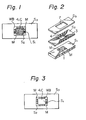
- Two types of mark structures are known for recognizing the location of a cavity provided in a semi- conductor package.
- marks M are formed within a metallized chip stage 1 on a first sheet S l , in a chip cavity C.
- a first window 4 is opened in a second sheet S 2 , on which an internal conductor pattern 3 is metallized so as to form a wire-bonding area WB.
- a second window is opened in a third sheet S 3 .
- the first window 4 and the second window 7 constitute the chip cavity C.
- the marks M are formed witnin the wire-bonding,area WB on the second sheet S 2 , in the chip cavity C ( Figure 3).
- the marks M and the internal conductor pattern 3 are printed simultaneously on the second sheet S 2 .
- the first window 4 is punched through the second sheet S 2 . Therefore, due to inappropriate registration between the printing and the punching, the mal-alignment of the marks in respect to the first window 4 amounts to ⁇ 0.1 mm.
- the clearance between the chip and the chip-cavity is inevitably limited by the amount of mal-alignment, i.e. ⁇ 0.1 0.2 mm.
- Figure 4 illustrates a plan of an example of a package according to the present invention.
- Figure 5 is a sectional view taken along the arrows "A" and "A"' in Figure 4.
- the package comprises three ceramic sheets 12, 16, and 19.
- the first sheet 12 is provided with a metallized chip stage 11, e.g., of gold.
- the second sheet 16 is provided with a metallized internal conductor pattern 13, e.g. of gold,a first chip-inserting window 14, and marks 15a and 15b for recognizing the location of the first chip-inserting window 14.
- the marks 15a and 15b are punched at the same time that the first chip-inserting window 14, which exposes the chip stage 11, is punched, the marks 15a and 15b and the window 14 being punched by the same mold.
- the third sheet 19 is provided with a cap-brazing frame 18, e.g., of Au-Sn, and a second chip-inserting window 17, which exposes a portion of the internal conductor pattern 13 and the first window 14. This exposed portion of the pattern 13 constitutes a wire-bonding area, which surrounds the first window 14.
- the cap-brazing frame 18 surrounds the second window 17.
- the first and the second chip-inserting windows 14 and 17 constitute the chip-cavity, in which a chip is to be mounted.
- External leads 21 are fixed to a brazing material 20, e.g., of silver and are superposed on the extended portions of the internal conductor pattern 13.
- marks 15a and 15b for recognizing the location of the first window 14 are formed in the wire-bonding area.
- the exposed surfaces of the external leads 21, the internal conductor pattern 13, and the chip stage 11 are usually plated, e.g., with gold.
- the package for semiconductor devices comprises three ceramic sheets.
- the first sheet has a conventional structure and is provided with the chip stage 11 and the metallized layer 22 in a conventional manner.
- the second sheet 16 is provided with the internal conductor pattern 13, the chip-inserting window 14, and the marks 15a and 15b.
- the window 14 and the marks 15a and 15b are simultaneously punched with the same mold through the second sheet 16.
- the third sheet 19 is provided with the second chip-inserting window 17 and the cap-brazing frame 18 metallized around the window 17 in a conventional manner.
Landscapes
- Die Bonding (AREA)
- Wire Bonding (AREA)
Applications Claiming Priority (2)
| Application Number | Priority Date | Filing Date | Title |
|---|---|---|---|
| JP56177888A JPS6038868B2 (ja) | 1981-11-06 | 1981-11-06 | 半導体パツケ−ジ |
| JP177888/81 | 1981-11-06 |
Publications (3)
| Publication Number | Publication Date |
|---|---|
| EP0079211A2 true EP0079211A2 (de) | 1983-05-18 |
| EP0079211A3 EP0079211A3 (en) | 1985-05-22 |
| EP0079211B1 EP0079211B1 (de) | 1989-01-18 |
Family
ID=16038808
Family Applications (1)
| Application Number | Title | Priority Date | Filing Date |
|---|---|---|---|
| EP82305890A Expired EP0079211B1 (de) | 1981-11-06 | 1982-11-05 | Packung für Halbleiteranordnung und Verfahren zu deren Herstellung |
Country Status (4)
| Country | Link |
|---|---|
| US (1) | US4710250A (de) |
| EP (1) | EP0079211B1 (de) |
| JP (1) | JPS6038868B2 (de) |
| DE (1) | DE3279378D1 (de) |
Cited By (2)
| Publication number | Priority date | Publication date | Assignee | Title |
|---|---|---|---|---|
| EP0415343A3 (en) * | 1989-08-28 | 1992-08-05 | Sumitomo Electric Industries, Limited | Integrated circuit device and method for manufacturing the same |
| US5196918A (en) * | 1989-08-28 | 1993-03-23 | Sumitomo Electric Industries, Ltd. | Integrated circuit device and method for manufacturing the same |
Families Citing this family (14)
| Publication number | Priority date | Publication date | Assignee | Title |
|---|---|---|---|---|
| JPS63191638U (de) * | 1987-05-28 | 1988-12-09 | ||
| JPH073874B2 (ja) * | 1987-07-22 | 1995-01-18 | 工業技術院長 | 半導体装置 |
| JPH0744234B2 (ja) * | 1987-09-30 | 1995-05-15 | 株式会社東芝 | 半導体装置用パッケージ |
| US5061428A (en) * | 1990-01-04 | 1991-10-29 | Davidson Textron Inc. | Method for plastic coating foam molding insert |
| FR2688929B1 (fr) * | 1992-03-23 | 1994-05-20 | Xeram | Procede d'obtention d'inserts ceramiques isolants par empilement multicouches. |
| US5455385A (en) * | 1993-06-28 | 1995-10-03 | Harris Corporation | Multilayer LTCC tub architecture for hermetically sealing semiconductor die, external electrical access for which is provided by way of sidewall recesses |
| US5478420A (en) * | 1994-07-28 | 1995-12-26 | International Business Machines Corporation | Process for forming open-centered multilayer ceramic substrates |
| US5728244A (en) * | 1995-05-26 | 1998-03-17 | Ngk Insulators, Ltd. | Process for production of ceramic member having fine throughholes |
| JP3420391B2 (ja) * | 1995-06-20 | 2003-06-23 | キヤノン株式会社 | 電気回路基板におけるアライメントマーク構造 |
| JP2803717B2 (ja) * | 1996-03-21 | 1998-09-24 | 日本電気株式会社 | チップ状遮断部品及びその回路修復装置 |
| US5858145A (en) * | 1996-10-15 | 1999-01-12 | Sarnoff Corporation | Method to control cavity dimensions of fired multilayer circuit boards on a support |
| US7975343B2 (en) * | 2002-09-20 | 2011-07-12 | Colgate-Palmolive Company | Toothbrush |
| FR2913529B1 (fr) * | 2007-03-09 | 2009-04-24 | E2V Semiconductors Soc Par Act | Boitier de circuit integre,notamment pour capteur d'image, et procede de positionnement |
| JP5430496B2 (ja) * | 2010-05-27 | 2014-02-26 | 京セラ株式会社 | 電子部品搭載用パッケージ |
Family Cites Families (9)
| Publication number | Priority date | Publication date | Assignee | Title |
|---|---|---|---|---|
| US3518756A (en) * | 1967-08-22 | 1970-07-07 | Ibm | Fabrication of multilevel ceramic,microelectronic structures |
| US3770529A (en) * | 1970-08-25 | 1973-11-06 | Ibm | Method of fabricating multilayer circuits |
| US3778686A (en) * | 1972-08-18 | 1973-12-11 | Motorola Inc | Carrier for beam lead integrated circuits |
| US4007479A (en) * | 1976-03-29 | 1977-02-08 | Honeywell Information Systems, Inc. | Fixture for an integrated circuit chip |
| US4066485A (en) * | 1977-01-21 | 1978-01-03 | Rca Corporation | Method of fabricating a semiconductor device |
| JPS5419360A (en) * | 1977-07-14 | 1979-02-14 | Oki Electric Ind Co Ltd | Ic case with resistors |
| WO1981000172A1 (en) * | 1979-07-04 | 1981-01-22 | Westinghouse Brake & Signal | Semiconductor contact shim and attachment method |
| US4288841A (en) * | 1979-09-20 | 1981-09-08 | Bell Telephone Laboratories, Incorporated | Double cavity semiconductor chip carrier |
| JPS5893862U (ja) * | 1981-12-21 | 1983-06-25 | 日本特殊陶業株式会社 | 酸素センサ |
-
1981
- 1981-11-06 JP JP56177888A patent/JPS6038868B2/ja not_active Expired
-
1982
- 1982-11-05 EP EP82305890A patent/EP0079211B1/de not_active Expired
- 1982-11-05 DE DE8282305890T patent/DE3279378D1/de not_active Expired
-
1986
- 1986-02-11 US US06/809,796 patent/US4710250A/en not_active Expired - Fee Related
Cited By (3)
| Publication number | Priority date | Publication date | Assignee | Title |
|---|---|---|---|---|
| EP0415343A3 (en) * | 1989-08-28 | 1992-08-05 | Sumitomo Electric Industries, Limited | Integrated circuit device and method for manufacturing the same |
| US5196918A (en) * | 1989-08-28 | 1993-03-23 | Sumitomo Electric Industries, Ltd. | Integrated circuit device and method for manufacturing the same |
| US5306669A (en) * | 1989-08-28 | 1994-04-26 | Sumitomo Electric Industries, Ltd. | Integrated circuit device and method for manufacturing the same |
Also Published As
| Publication number | Publication date |
|---|---|
| JPS5879725A (ja) | 1983-05-13 |
| EP0079211B1 (de) | 1989-01-18 |
| DE3279378D1 (en) | 1989-02-23 |
| JPS6038868B2 (ja) | 1985-09-03 |
| US4710250A (en) | 1987-12-01 |
| EP0079211A3 (en) | 1985-05-22 |
Similar Documents
| Publication | Publication Date | Title |
|---|---|---|
| EP0079211B1 (de) | Packung für Halbleiteranordnung und Verfahren zu deren Herstellung | |
| US5369545A (en) | De-coupling capacitor on the top of the silicon die by eutectic flip bonding | |
| US5006673A (en) | Fabrication of pad array carriers from a universal interconnect structure | |
| KR20030044838A (ko) | 반도체장치 | |
| US6879034B1 (en) | Semiconductor package including low temperature co-fired ceramic substrate | |
| US5953594A (en) | Method of making a circuitized substrate for chip carrier structure | |
| JP3093960B2 (ja) | 半導体回路素子搭載基板フレームの製造方法 | |
| EP3367764A1 (de) | Mehrschichtiger keramikträger und verfahren zur herstellung davon | |
| US6225028B1 (en) | Method of making an enhanced organic chip carrier package | |
| US5496967A (en) | Package for holding IC chip | |
| US6476470B1 (en) | Integrated circuit packaging | |
| JP3988250B2 (ja) | 多層回路基板の製造方法 | |
| JPH05206308A (ja) | 表面実装部品 | |
| JP3488826B2 (ja) | 配線基板用多数個取り基板 | |
| JPH0992780A (ja) | 多層配線基板及び表面実装型電子部品の実装方法 | |
| US5429859A (en) | LTCC alignment marks for mechanical parts placement | |
| JP2943773B2 (ja) | Icパッケージ | |
| KR100519813B1 (ko) | 다층기판의 단자구조 및 그 형성방법 | |
| JPH07112107B2 (ja) | プリント配線板及びその製造方法 | |
| EP0698921B1 (de) | Anordnung mit einer mehrschichtigen Leiterplatte und einem Träger | |
| EP0100727B1 (de) | Halbleiteranordnung mit einem keramischen Träger | |
| JP2004111849A (ja) | セラミック配線基板、それを用いた部品実装済み配線基板、及びそれらの製造方法 | |
| JP3104680B2 (ja) | 半導体装置の封止用キャップ及びその製造方法 | |
| US20020027011A1 (en) | Multi-chip module made of a low temperature co-fired ceramic and mounting method thereof | |
| JPH06326471A (ja) | 多層配線基板 |
Legal Events
| Date | Code | Title | Description |
|---|---|---|---|
| PUAI | Public reference made under article 153(3) epc to a published international application that has entered the european phase |
Free format text: ORIGINAL CODE: 0009012 |
|
| AK | Designated contracting states |
Designated state(s): DE FR GB |
|
| PUAL | Search report despatched |
Free format text: ORIGINAL CODE: 0009013 |
|
| AK | Designated contracting states |
Designated state(s): DE FR GB |
|
| 17P | Request for examination filed |
Effective date: 19851111 |
|
| 17Q | First examination report despatched |
Effective date: 19870615 |
|
| GRAA | (expected) grant |
Free format text: ORIGINAL CODE: 0009210 |
|
| AK | Designated contracting states |
Kind code of ref document: B1 Designated state(s): DE FR GB |
|
| REF | Corresponds to: |
Ref document number: 3279378 Country of ref document: DE Date of ref document: 19890223 |
|
| ET | Fr: translation filed | ||
| PLBE | No opposition filed within time limit |
Free format text: ORIGINAL CODE: 0009261 |
|
| STAA | Information on the status of an ep patent application or granted ep patent |
Free format text: STATUS: NO OPPOSITION FILED WITHIN TIME LIMIT |
|
| 26N | No opposition filed | ||
| PGFP | Annual fee paid to national office [announced via postgrant information from national office to epo] |
Ref country code: GB Payment date: 19921026 Year of fee payment: 11 |
|
| PGFP | Annual fee paid to national office [announced via postgrant information from national office to epo] |
Ref country code: FR Payment date: 19921127 Year of fee payment: 11 |
|
| PGFP | Annual fee paid to national office [announced via postgrant information from national office to epo] |
Ref country code: DE Payment date: 19930129 Year of fee payment: 11 |
|
| PG25 | Lapsed in a contracting state [announced via postgrant information from national office to epo] |
Ref country code: GB Effective date: 19931105 |
|
| GBPC | Gb: european patent ceased through non-payment of renewal fee |
Effective date: 19931105 |
|
| PG25 | Lapsed in a contracting state [announced via postgrant information from national office to epo] |
Ref country code: FR Effective date: 19940729 |
|
| PG25 | Lapsed in a contracting state [announced via postgrant information from national office to epo] |
Ref country code: DE Effective date: 19940802 |
|
| REG | Reference to a national code |
Ref country code: FR Ref legal event code: ST |