EP0097918B1 - Halbleiteranordnung und Verfahren zu ihrer Herstellung - Google Patents
Halbleiteranordnung und Verfahren zu ihrer Herstellung Download PDFInfo
- Publication number
- EP0097918B1 EP0097918B1 EP83106119A EP83106119A EP0097918B1 EP 0097918 B1 EP0097918 B1 EP 0097918B1 EP 83106119 A EP83106119 A EP 83106119A EP 83106119 A EP83106119 A EP 83106119A EP 0097918 B1 EP0097918 B1 EP 0097918B1
- Authority
- EP
- European Patent Office
- Prior art keywords
- film
- forming
- substrate
- polycrystalline silicon
- polycrystalline
- Prior art date
- Legal status (The legal status is an assumption and is not a legal conclusion. Google has not performed a legal analysis and makes no representation as to the accuracy of the status listed.)
- Expired
Links
Images



Classifications
-
- H—ELECTRICITY
- H10—SEMICONDUCTOR DEVICES; ELECTRIC SOLID-STATE DEVICES NOT OTHERWISE PROVIDED FOR
- H10W—GENERIC PACKAGES, INTERCONNECTIONS, CONNECTORS OR OTHER CONSTRUCTIONAL DETAILS OF DEVICES COVERED BY CLASS H10
- H10W20/00—Interconnections in chips, wafers or substrates
- H10W20/01—Manufacture or treatment
- H10W20/031—Manufacture or treatment of conductive parts of the interconnections
- H10W20/064—Manufacture or treatment of conductive parts of the interconnections by modifying the conductivity of conductive parts, e.g. by alloying
- H10W20/066—Manufacture or treatment of conductive parts of the interconnections by modifying the conductivity of conductive parts, e.g. by alloying by forming silicides of refractory metals
-
- H—ELECTRICITY
- H10—SEMICONDUCTOR DEVICES; ELECTRIC SOLID-STATE DEVICES NOT OTHERWISE PROVIDED FOR
- H10D—INORGANIC ELECTRIC SEMICONDUCTOR DEVICES
- H10D30/00—Field-effect transistors [FET]
- H10D30/60—Insulated-gate field-effect transistors [IGFET]
-
- H—ELECTRICITY
- H10—SEMICONDUCTOR DEVICES; ELECTRIC SOLID-STATE DEVICES NOT OTHERWISE PROVIDED FOR
- H10W—GENERIC PACKAGES, INTERCONNECTIONS, CONNECTORS OR OTHER CONSTRUCTIONAL DETAILS OF DEVICES COVERED BY CLASS H10
- H10W20/00—Interconnections in chips, wafers or substrates
- H10W20/01—Manufacture or treatment
- H10W20/031—Manufacture or treatment of conductive parts of the interconnections
- H10W20/056—Manufacture or treatment of conductive parts of the interconnections by filling conductive material into holes, grooves or trenches
- H10W20/057—Manufacture or treatment of conductive parts of the interconnections by filling conductive material into holes, grooves or trenches by selectively depositing, e.g. by using selective CVD or plating
-
- H—ELECTRICITY
- H10—SEMICONDUCTOR DEVICES; ELECTRIC SOLID-STATE DEVICES NOT OTHERWISE PROVIDED FOR
- H10W—GENERIC PACKAGES, INTERCONNECTIONS, CONNECTORS OR OTHER CONSTRUCTIONAL DETAILS OF DEVICES COVERED BY CLASS H10
- H10W20/00—Interconnections in chips, wafers or substrates
- H10W20/40—Interconnections external to wafers or substrates, e.g. back-end-of-line [BEOL] metallisations or vias connecting to gate electrodes
- H10W20/41—Interconnections external to wafers or substrates, e.g. back-end-of-line [BEOL] metallisations or vias connecting to gate electrodes characterised by their conductive parts
- H10W20/44—Conductive materials thereof
- H10W20/4403—Conductive materials thereof based on metals, e.g. alloys, metal silicides
- H10W20/4437—Conductive materials thereof based on metals, e.g. alloys, metal silicides the principal metal being a transition metal
- H10W20/4441—Conductive materials thereof based on metals, e.g. alloys, metal silicides the principal metal being a transition metal the principal metal being a refractory metal
-
- H—ELECTRICITY
- H10—SEMICONDUCTOR DEVICES; ELECTRIC SOLID-STATE DEVICES NOT OTHERWISE PROVIDED FOR
- H10W—GENERIC PACKAGES, INTERCONNECTIONS, CONNECTORS OR OTHER CONSTRUCTIONAL DETAILS OF DEVICES COVERED BY CLASS H10
- H10W20/00—Interconnections in chips, wafers or substrates
- H10W20/40—Interconnections external to wafers or substrates, e.g. back-end-of-line [BEOL] metallisations or vias connecting to gate electrodes
- H10W20/41—Interconnections external to wafers or substrates, e.g. back-end-of-line [BEOL] metallisations or vias connecting to gate electrodes characterised by their conductive parts
- H10W20/44—Conductive materials thereof
- H10W20/4451—Semiconductor materials, e.g. polysilicon
-
- Y—GENERAL TAGGING OF NEW TECHNOLOGICAL DEVELOPMENTS; GENERAL TAGGING OF CROSS-SECTIONAL TECHNOLOGIES SPANNING OVER SEVERAL SECTIONS OF THE IPC; TECHNICAL SUBJECTS COVERED BY FORMER USPC CROSS-REFERENCE ART COLLECTIONS [XRACs] AND DIGESTS
- Y10—TECHNICAL SUBJECTS COVERED BY FORMER USPC
- Y10S—TECHNICAL SUBJECTS COVERED BY FORMER USPC CROSS-REFERENCE ART COLLECTIONS [XRACs] AND DIGESTS
- Y10S148/00—Metal treatment
- Y10S148/02—Contacts, special
Definitions
- the present invention relates to a method for making a semiconductor device.
- the present invention specially concerns a method for making a semiconductor device principally comprising MOS FET intending to achieve higher integration and lower wiring resistance.
- MOS IC or MOS LSI polycrystalline silicon pattern and aluminum wiring pattern provided on a substrate with an insulation film in between together with combined diffused regions formed in the substrate are widely used.
- wiring between them and interconnection between the wirings become more difficult, and the wiring and the unit devices are likely to be destroyed durcing the wiring process, and this forms shortcoming in the manufacturing of the semiconductor IC or LSI.
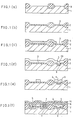
- FIG. 1(a) to Fig. 1(f) show prior art steps of manufacturing an N-channel silicon gate MOS LSI as an example embodying the prior art connections between polycrystalline silicon layer and diffused region.
- Fig. 1(a) on a principal surface of a P-type silicon substrate, isolation regions of thick film of oxide of silicon are formed by known selective oxidation method. Then, as shown in Fig. 1 (b), gate-oxide film 3 shown in Fig. 1 (b) is formed by, for instance, thermal oxidation. Nextly, as shown in Fig. 1(c), photoresist film of a desired mask pattern for forming the gate-oxide film 3 is formed in order to make an opening 39 on the gate-oxide film 3, by chemical etching by using fluoric acid-fluoroammonium mixed solution is carried out.
- the photoresist film 4 is removed by known method, and as shown in Fig. 1 (d), a polycrystalline silicon layer 5 is formed thereon. Thereafter, phosphorus is diffused on the polycrystalline layer 5 by known thermal diffusion method thereby to increase electric conductivity. Simultaneously, phosphorus is diffused in the substrate 1 to form N +- diffused region 6, which is to be connected to the polycrystalline layer 5. Then, as shown in Fig. 1(e), the polycrystalline silicon layer 5 is etched to a predetermined pattern. And then as shown in Fig.
- N +- diffusion regions 7 to become source and drain are formed in the substrate 1 by ion- implanting phosphorus or arsenic by known method, and thereon an interlayer insulation film 8 is formed. After forming electrode contact openings on the insulation films 8, 3, aluminum alloy electrodes 9 is formed therein, and then protection film 10 is formed thereon.
- connections between the first polycrystalline silicon layer and the diffused region on the substrate and connection between the second polycrystalline silicon layer and the diffused region in the substrate and connection between the first polycrystalline layer and the second polycrystalline layer would be made in accordance with the preceding prior art example. Accordingly, in such double-layered polycrystalline silicon structure, steps of forming opening in the insulation film becomes necessarily twice.
- the prior art making of the MOS FET uses lithographic etching of the gate-oxide film, and therefore when the photoresist film has a pinhole or the like defect the obtained gate-oxide film has a pinhole or defect, thereby the gate-oxide film resultantly has a pinhole, to shortcircuit the substrate and the polycrystalline silicon film. Furthermore, removing of the photoresist film after the etching is made by immersing the substrate into fuming nitric acid or the like to be used for the resist removal or by applying oxygen plasma etching, accordingly, the gate-oxide film is likely to be polluted with heavy metal or the like impurities in the etching agent or in the photoresist.
- the prior art method makes thin oxide film of about 1 nm on the surface of the silicon substrate, accordingly, there is a necessity of a step of removing the thin oxide film by chemical etching by fluoric acid prior to formation of polycrystalline silicon layer on the substrate before the formation of polycrystalline silicon layer. And at this step the gate-oxide film is also etched to some extent, and therefore irregular parts may be formed on the surface of the gate-oxide film and such influence is especially adverse when the gate-oxide film becomes thinner as the individual element of the IC or LSI becomes designed more and more small.
- the present invention has the purpose to remove the above-mentioned shortcoming, and provides an easier and reliable method for making a semiconductor device comprising wirings formed by polycrystalline silicon layers, diffused regions and their interconnections without lowering the reliability of connections.
- the method for making the semiconductor device in accordance with the present invention comprises the steps of:
- Fig. 2 is a sectional elevation view of a semiconductor device of N-channel MOS FET made in accordance with the method of the present invention.
- the parts corresponding to the device shown in Fig. 1 are designated with the same numerals as those of Fig. 1.
- the semiconductor device comprises on a semiconductor substrate 1 of a first conductivity type, at least an impurity-diffused region 11 e.g. of a second conductivity type such as opposite to said first conductivity type, at least a polycrystalline semiconductor layer 5 formed on an insulation film 3 on the substrate 1 to surround said impurity diffused region 11, and a conductive film 12, such as tungsten film formed by chemical vapor deposition (hereinafter referred to CVD), formed to connect said impurity diffused region 11 exposed from an opening 31 formed through the insulation film 3 and said polycrystalline semiconductor layer 5 in the above-mentioned configuration.
- CVD chemical vapor deposition
- the diffused region 11 is formed by known thermal diffusion method through opening 51 formed on the polycrystalline silicon layer 5, which is formed on the insulation film 3, such as silicon dioxide film formed simultaneously with the forming of the gate oxide film. Therefore, the diffused region 11 is formed in self-alignment relation with the opening 51 of the polycrystalline silicon layer 5.
- the other part of the polycrystalline silicon layer 5, which is formed on, for instance, a part to become a gate oxide film 3' of the insulation film serves as a gate electrode 5' and is connected with the previously said polycrystalline silicon layer 5 around and above the diffused region 11.
- the diffused region 11 and the polycrystalline silicon layer 5 are connected by the CVD-formed conductive film 12 and also connected to the gate electrode 5' by the polycrystalline silicon layer in between.
- This semiconductor device can be made without undesirable direct chemical etching of gate oxide film through a photoresist mask, accordingly the quality of the gate oxide film is not lowered by the direct chemical etching. Since tungsten film 12 which is about 200 nm and has such a low sheet resistance of about 1 0/D, the conductivity between the diffused region 11 and the polycrystalline silicon layer 5 is sufficiently low, thereby providing a satisfactory IC performance.
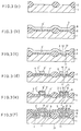
- Fig. 3(a), Fig. 3(b), Fig. 3(c), Fig. 3(d), Fig. 3(e) and Fig. 3(f) show manufacturing steps of the semiconductor device of Fig. 2.
- a thick oxide film 2 is selectively formed on a principal face of a p-type silicon substrate by means of selective oxidation method so as to form isolation regions between unit devices on the IC.
- gate oxide film 3 is formed on the substrate surface by a known method, and thereon a polycrystalline silicon layer 5 is formed to a thickness of 0.5 pm (5000 A).
- a complex opening 31, 51 is formed on the polycrystalline silicon layer 5 and the underlying silicon dioxide film 3.
- the polycrystalline silicon layer 5 is etched to a predetermined pattern as shown in Fig. 3(d). That is, the polycrystalline silicon layer 5 is retained in a ring shape on the insulation film 3 which is on the substrate 1 and around the diffused region 11, and also the polycrystalline silicon layer 5' is retained on the oxide film 3' which is to become a gate oxide film.
- a tungsten film 12 is formed by means of known low pressure vapor desposition method utilizing tungstenhexafluoride and hydrogen gas.
- the tungsten film 12 is not formed on silicon dioxide film, and grows only on the surfaces of polycrystalline silicon layer 5 and exposed surface of the silicon substrate 1. Therefore, as shown in Fig. 3(e), the polycrystalline silicon layer 5 and the diffused region 11 are connected by the tungsten film formed in self-alignment way. Then, as shown in Fig. 3(f), a silicon nitride film 8 as interlayer insulation film is formed by known plasma growth method. Nextly, openings for electrode connection are formed and electrodes 9 are formed by means of known aluminum alloy, and thereon a known passivation film 10 is formed by known method.
- Example 2
- Fig. 4(a), Fig. 4(b), Fig. 4(c), Fig. 4(d), Fig. 4(e), Fig. 4(f) and Fig. 4(g) shown manufacturing steps of a second example semiconductor device, wherein double layers of polycrystalline regions are comprised.
- a thick oxide film 2 is formed on a principal face of a substrate 1 to serve as isolation regions.
- gate oxide film 3 is formed by known method on the principal face of the substrate 1, and thereon a polycrystalline silicon layer 5 is formed with specified pattern produced by known photolithographic method.
- a polycrystalline silicon layer 5 is formed with specified pattern produced by known photolithographic method.
- Fig. 4(c) by forming the diffused regions 7 and 7' for source and drain regions by ion-implantation of P or As utilizing the polycrystalline silicon layer 5 as mask, followed by thermal treatment. Then by oxidizing the surface of the polycrystalline silicon layer 5, inter-layer insulation film 13 is formed, and simultaneously, the oxide films 14 on the diffused regions 7 and 7' are formed. And thereon, a second polycrystalline silicon layer 15 is formed.
- the second polycrystalline silicon layer 15 is etched to form a predetermined pattern.
- a first complex opening 151, 131 at the rightest part of Fig. 4(e) is formed to expose the first polycrystalline silicon buried layer 5; also, a second complex opening 131', 5T, 141 to expose the diffused region 16 on the leftest part of Fig. 4(e), and a third complex opening 151' 14' to expose the diffused regions 7 at the central part of Fig. 4(e) are formed by known photolithographic method.
- etchings to form complex openings are formed by using one photoresist mask having three openings for the first complex opening, the second complex opening and the third complex opening. And the etchings for forming three complex openings are made substantially at the same time. That is, firstly the interlayer insulation film 13 is etched to form the opening and thereafter the polycrystalline silicon layer 15 and 5 are etched, and thereafter, the intelayer insulation film 13 or 3 is etched. Then, P or As as impurity is introduced on the first polycrystalline silicon layer 5 and exposed region 16 to make them N +- type conductivity wiring and N +- type diffused region 16. Thereafter, as shown in Fig.
- tungsten electrodes 12 are deposited by a low-pressure chemical vapor deposition selec- tiely on the surfaces of the second polycrystalline silicon layer 15 and in three complex openings. Then, after forming an interlayer insulation film 8 by known plasma growth method followed by forming of known A1-alloy electrodes (not shown) to contact the diffused region 16 and the tungsten film 12 on the polycrystalline film 15, 5 as wirings in the part not shown in Fig. 4(g), the semiconductor device is completed.
- the semiconductor device made in accordance with the present invention elucidated in the above-mentioned examples can be manufactured by utilizing a single mask for boring the openings for connection between the polycrystalline silicon layers or between the polycrystalline silicon layer and impurity diffused regions, in contradistinction to the problematic conventional method which utilizes two separate photoresist masks.
- any other conductive substance which has a selective deposition characteristic with respect to the silicon is usable.
- the semiconductor device made in accordance with the present invention especially a MOS device, has a superior stability and high production yield as a result of elimination of direct chemical etching of the gate oxide film, since such etching is made indirectly with the polycrystalline silicon layer formed over it, preventing pollution and generation of pin-holes of the gate oxide film.
Landscapes
- Internal Circuitry In Semiconductor Integrated Circuit Devices (AREA)
- Electrodes Of Semiconductors (AREA)
Claims (3)
Applications Claiming Priority (2)
| Application Number | Priority Date | Filing Date | Title |
|---|---|---|---|
| JP110176/82 | 1982-06-25 | ||
| JP57110176A JPH0618213B2 (ja) | 1982-06-25 | 1982-06-25 | 半導体装置の製造方法 |
Publications (2)
| Publication Number | Publication Date |
|---|---|
| EP0097918A1 EP0097918A1 (de) | 1984-01-11 |
| EP0097918B1 true EP0097918B1 (de) | 1988-03-16 |
Family
ID=14528970
Family Applications (1)
| Application Number | Title | Priority Date | Filing Date |
|---|---|---|---|
| EP83106119A Expired EP0097918B1 (de) | 1982-06-25 | 1983-06-22 | Halbleiteranordnung und Verfahren zu ihrer Herstellung |
Country Status (4)
| Country | Link |
|---|---|
| US (1) | US4948756A (de) |
| EP (1) | EP0097918B1 (de) |
| JP (1) | JPH0618213B2 (de) |
| DE (1) | DE3376043D1 (de) |
Families Citing this family (14)
| Publication number | Priority date | Publication date | Assignee | Title |
|---|---|---|---|---|
| JPS60138940A (ja) * | 1983-12-27 | 1985-07-23 | Toshiba Corp | 半導体装置の製造方法 |
| DE3569172D1 (en) * | 1984-08-23 | 1989-05-03 | Toshiba Kk | Semiconductor memory device having a polycrystalline silicon layer |
| EP0201250B1 (de) * | 1985-04-26 | 1992-01-29 | Fujitsu Limited | Verfahren zur Herstellung einer Kontaktanordnung für eine Halbleiteranordnung |
| JPS63187580U (de) * | 1987-05-22 | 1988-12-01 | ||
| JP2757927B2 (ja) * | 1990-06-28 | 1998-05-25 | インターナショナル・ビジネス・マシーンズ・コーポレイション | 半導体基板上の隔置されたシリコン領域の相互接続方法 |
| KR920010759A (ko) * | 1990-11-16 | 1992-06-27 | 원본미기재 | 저 저항 접점을 제조하는 방법 |
| US5124280A (en) * | 1991-01-31 | 1992-06-23 | Sgs-Thomson Microelectronics, Inc. | Local interconnect for integrated circuits |
| US5332913A (en) * | 1991-12-17 | 1994-07-26 | Intel Corporation | Buried interconnect structure for semiconductor devices |
| KR950011555B1 (ko) * | 1992-06-16 | 1995-10-06 | 현대전자산업주식회사 | 반도체 접속장치 및 그 제조방법 |
| JP2658899B2 (ja) * | 1994-09-22 | 1997-09-30 | 日本電気株式会社 | 半導体装置の製造方法 |
| US6740573B2 (en) * | 1995-02-17 | 2004-05-25 | Micron Technology, Inc. | Method for forming an integrated circuit interconnect using a dual poly process |
| US5640859C1 (en) * | 1996-01-24 | 2001-11-27 | Wayne G Fromm | Tie-dyeing kit |
| US6010935A (en) * | 1997-08-21 | 2000-01-04 | Micron Technology, Inc. | Self aligned contacts |
| US7309906B1 (en) * | 2004-04-01 | 2007-12-18 | Altera Corporation | Apparatus and methods for providing highly effective and area efficient decoupling capacitance in programmable logic devices |
Citations (5)
| Publication number | Priority date | Publication date | Assignee | Title |
|---|---|---|---|---|
| US3544399A (en) * | 1966-10-26 | 1970-12-01 | Hughes Aircraft Co | Insulated gate field-effect transistor (igfet) with semiconductor gate electrode |
| US3750268A (en) * | 1971-09-10 | 1973-08-07 | Motorola Inc | Poly-silicon electrodes for c-igfets |
| EP0008774A1 (de) * | 1978-09-01 | 1980-03-19 | Teletype Corporation | Verfahren zum Herstellen einer Vorrichtung in einer Siliziumscheibe |
| EP0032195A1 (de) * | 1979-12-28 | 1981-07-22 | International Business Machines Corporation | Schottky-Sperrschichtdiode und Verfahren zu deren Herstellung |
| EP0054163A2 (de) * | 1980-12-05 | 1982-06-23 | International Business Machines Corporation | Verfahren zur Herstellung eines elektrischen Kontakts zu einem Siliziumsubstrat durch eine auf einer Substratoberfläche angebrachte, verhältnismässig dünne Schicht aus Siliziumdioxyd und Verfahren zur Herstellung eines Feldeffekttransistors |
Family Cites Families (11)
| Publication number | Priority date | Publication date | Assignee | Title |
|---|---|---|---|---|
| US3266127A (en) * | 1964-01-27 | 1966-08-16 | Ibm | Method of forming contacts on semiconductors |
| JPS5451783A (en) * | 1977-09-30 | 1979-04-23 | Matsushita Electric Ind Co Ltd | Manufacture of mos-type semiconductor device |
| JPS6055988B2 (ja) * | 1979-01-26 | 1985-12-07 | 株式会社日立製作所 | 半導体装置の製法 |
| US4305200A (en) * | 1979-11-06 | 1981-12-15 | Hewlett-Packard Company | Method of forming self-registering source, drain, and gate contacts for FET transistor structures |
| JPS5736844A (en) * | 1980-08-15 | 1982-02-27 | Hitachi Ltd | Semiconductor device |
| US4374700A (en) * | 1981-05-29 | 1983-02-22 | Texas Instruments Incorporated | Method of manufacturing silicide contacts for CMOS devices |
| JPS59220952A (ja) * | 1983-05-31 | 1984-12-12 | Toshiba Corp | 半導体装置の製造方法 |
| US4441247A (en) * | 1981-06-29 | 1984-04-10 | Intel Corporation | Method of making MOS device by forming self-aligned polysilicon and tungsten composite gate |
| JPS584924A (ja) * | 1981-07-01 | 1983-01-12 | Hitachi Ltd | 半導体装置の電極形成方法 |
| JPS58175846A (ja) * | 1982-04-08 | 1983-10-15 | Toshiba Corp | 半導体装置の製造方法 |
| JPH02886A (ja) * | 1988-02-08 | 1990-01-05 | Minolta Camera Co Ltd | 画像形成装置の駆動方法 |
-
1982
- 1982-06-25 JP JP57110176A patent/JPH0618213B2/ja not_active Expired - Lifetime
-
1983
- 1983-06-22 DE DE8383106119T patent/DE3376043D1/de not_active Expired
- 1983-06-22 EP EP83106119A patent/EP0097918B1/de not_active Expired
-
1988
- 1988-10-28 US US07/265,355 patent/US4948756A/en not_active Expired - Lifetime
Patent Citations (5)
| Publication number | Priority date | Publication date | Assignee | Title |
|---|---|---|---|---|
| US3544399A (en) * | 1966-10-26 | 1970-12-01 | Hughes Aircraft Co | Insulated gate field-effect transistor (igfet) with semiconductor gate electrode |
| US3750268A (en) * | 1971-09-10 | 1973-08-07 | Motorola Inc | Poly-silicon electrodes for c-igfets |
| EP0008774A1 (de) * | 1978-09-01 | 1980-03-19 | Teletype Corporation | Verfahren zum Herstellen einer Vorrichtung in einer Siliziumscheibe |
| EP0032195A1 (de) * | 1979-12-28 | 1981-07-22 | International Business Machines Corporation | Schottky-Sperrschichtdiode und Verfahren zu deren Herstellung |
| EP0054163A2 (de) * | 1980-12-05 | 1982-06-23 | International Business Machines Corporation | Verfahren zur Herstellung eines elektrischen Kontakts zu einem Siliziumsubstrat durch eine auf einer Substratoberfläche angebrachte, verhältnismässig dünne Schicht aus Siliziumdioxyd und Verfahren zur Herstellung eines Feldeffekttransistors |
Also Published As
| Publication number | Publication date |
|---|---|
| DE3376043D1 (en) | 1988-04-21 |
| EP0097918A1 (de) | 1984-01-11 |
| JPS59965A (ja) | 1984-01-06 |
| US4948756A (en) | 1990-08-14 |
| JPH0618213B2 (ja) | 1994-03-09 |
Similar Documents
| Publication | Publication Date | Title |
|---|---|---|
| US6614098B1 (en) | Semiconductor devices and fabrication thereof | |
| US4528744A (en) | Method of manufacturing a semiconductor device | |
| EP0097918B1 (de) | Halbleiteranordnung und Verfahren zu ihrer Herstellung | |
| JPH0228902B2 (de) | ||
| KR910006674B1 (ko) | 반도체 장치의 제조방법 | |
| US3967364A (en) | Method of manufacturing semiconductor devices | |
| JPS5922342A (ja) | 半導体装置の製造方法 | |
| JPS61183967A (ja) | 半導体装置の製造方法 | |
| JPS6138858B2 (de) | ||
| JPH0127589B2 (de) | ||
| JPS63147318A (ja) | 半導体装置及びその製造方法 | |
| JPH0554263B2 (de) | ||
| JPS6197825A (ja) | 半導体装置の製造方法 | |
| JPS62122173A (ja) | 半導体装置 | |
| JPS61256672A (ja) | 半導体装置の製造方法 | |
| JPS61166143A (ja) | 半導体装置の製造方法 | |
| JPS58191466A (ja) | Mos型トランジスタの製造方法 | |
| JPS61154150A (ja) | 半導体装置の製造方法 | |
| JPS6161546B2 (de) | ||
| JPH0410620A (ja) | 半導体装置の製造方法 | |
| JPH0629288A (ja) | 半導体装置及びその製造方法 | |
| JPH09171974A (ja) | 半導体装置の製造方法 | |
| JPH0547938A (ja) | 半導体装置およびその製造方法 | |
| JPH0312768B2 (de) | ||
| JPS6255702B2 (de) |
Legal Events
| Date | Code | Title | Description |
|---|---|---|---|
| PUAI | Public reference made under article 153(3) epc to a published international application that has entered the european phase |
Free format text: ORIGINAL CODE: 0009012 |
|
| AK | Designated contracting states |
Designated state(s): DE FR GB |
|
| 17P | Request for examination filed |
Effective date: 19840319 |
|
| GRAA | (expected) grant |
Free format text: ORIGINAL CODE: 0009210 |
|
| AK | Designated contracting states |
Kind code of ref document: B1 Designated state(s): DE FR GB |
|
| REF | Corresponds to: |
Ref document number: 3376043 Country of ref document: DE Date of ref document: 19880421 |
|
| ET | Fr: translation filed | ||
| PLBE | No opposition filed within time limit |
Free format text: ORIGINAL CODE: 0009261 |
|
| STAA | Information on the status of an ep patent application or granted ep patent |
Free format text: STATUS: NO OPPOSITION FILED WITHIN TIME LIMIT |
|
| 26N | No opposition filed | ||
| PGFP | Annual fee paid to national office [announced via postgrant information from national office to epo] |
Ref country code: FR Payment date: 19970610 Year of fee payment: 15 |
|
| PGFP | Annual fee paid to national office [announced via postgrant information from national office to epo] |
Ref country code: GB Payment date: 19970613 Year of fee payment: 15 |
|
| PGFP | Annual fee paid to national office [announced via postgrant information from national office to epo] |
Ref country code: DE Payment date: 19970630 Year of fee payment: 15 |
|
| PG25 | Lapsed in a contracting state [announced via postgrant information from national office to epo] |
Ref country code: GB Free format text: LAPSE BECAUSE OF NON-PAYMENT OF DUE FEES Effective date: 19980622 |
|
| GBPC | Gb: european patent ceased through non-payment of renewal fee |
Effective date: 19980622 |
|
| PG25 | Lapsed in a contracting state [announced via postgrant information from national office to epo] |
Ref country code: FR Free format text: LAPSE BECAUSE OF NON-PAYMENT OF DUE FEES Effective date: 19990226 |
|
| PG25 | Lapsed in a contracting state [announced via postgrant information from national office to epo] |
Ref country code: DE Free format text: LAPSE BECAUSE OF NON-PAYMENT OF DUE FEES Effective date: 19990401 |
|
| REG | Reference to a national code |
Ref country code: FR Ref legal event code: ST |