EP0152116A2 - Transistor bipolaire latéral et son procédé de fabrication - Google Patents
Transistor bipolaire latéral et son procédé de fabrication Download PDFInfo
- Publication number
- EP0152116A2 EP0152116A2 EP85101688A EP85101688A EP0152116A2 EP 0152116 A2 EP0152116 A2 EP 0152116A2 EP 85101688 A EP85101688 A EP 85101688A EP 85101688 A EP85101688 A EP 85101688A EP 0152116 A2 EP0152116 A2 EP 0152116A2
- Authority
- EP
- European Patent Office
- Prior art keywords
- region
- conductivity type
- single crystal
- bipolar transistor
- lateral bipolar
- Prior art date
- Legal status (The legal status is an assumption and is not a legal conclusion. Google has not performed a legal analysis and makes no representation as to the accuracy of the status listed.)
- Granted
Links
Images




Classifications
-
- H—ELECTRICITY
- H10—SEMICONDUCTOR DEVICES; ELECTRIC SOLID-STATE DEVICES NOT OTHERWISE PROVIDED FOR
- H10D—INORGANIC ELECTRIC SEMICONDUCTOR DEVICES
- H10D64/00—Electrodes of devices having potential barriers
- H10D64/01—Manufacture or treatment
- H10D64/011—Manufacture or treatment of electrodes ohmically coupled to a semiconductor
- H10D64/0111—Manufacture or treatment of electrodes ohmically coupled to a semiconductor to Group IV semiconductors
- H10D64/0113—Manufacture or treatment of electrodes ohmically coupled to a semiconductor to Group IV semiconductors the conductive layers comprising highly doped semiconductor materials, e.g. polysilicon layers or amorphous silicon layers
-
- H—ELECTRICITY
- H10—SEMICONDUCTOR DEVICES; ELECTRIC SOLID-STATE DEVICES NOT OTHERWISE PROVIDED FOR
- H10D—INORGANIC ELECTRIC SEMICONDUCTOR DEVICES
- H10D10/00—Bipolar junction transistors [BJT]
- H10D10/60—Lateral BJTs
-
- H—ELECTRICITY
- H10—SEMICONDUCTOR DEVICES; ELECTRIC SOLID-STATE DEVICES NOT OTHERWISE PROVIDED FOR
- H10D—INORGANIC ELECTRIC SEMICONDUCTOR DEVICES
- H10D62/00—Semiconductor bodies, or regions thereof, of devices having potential barriers
- H10D62/10—Shapes, relative sizes or dispositions of the regions of the semiconductor bodies; Shapes of the semiconductor bodies
- H10D62/17—Semiconductor regions connected to electrodes not carrying current to be rectified, amplified or switched, e.g. channel regions
- H10D62/177—Base regions of bipolar transistors, e.g. BJTs or IGBTs
- H10D62/184—Base regions of bipolar transistors, e.g. BJTs or IGBTs of lateral BJTs
-
- H—ELECTRICITY
- H10—SEMICONDUCTOR DEVICES; ELECTRIC SOLID-STATE DEVICES NOT OTHERWISE PROVIDED FOR
- H10P—GENERIC PROCESSES OR APPARATUS FOR THE MANUFACTURE OR TREATMENT OF DEVICES COVERED BY CLASS H10
- H10P32/00—Diffusion of dopants within, into or out of wafers, substrates or parts of devices
- H10P32/10—Diffusion of dopants within, into or out of semiconductor bodies or layers
- H10P32/14—Diffusion of dopants within, into or out of semiconductor bodies or layers within a single semiconductor body or layer in a solid phase; between different semiconductor bodies or layers, both in a solid phase
- H10P32/1408—Diffusion of dopants within, into or out of semiconductor bodies or layers within a single semiconductor body or layer in a solid phase; between different semiconductor bodies or layers, both in a solid phase from or through or into an external applied layer, e.g. photoresist or nitride layers
- H10P32/1414—Diffusion of dopants within, into or out of semiconductor bodies or layers within a single semiconductor body or layer in a solid phase; between different semiconductor bodies or layers, both in a solid phase from or through or into an external applied layer, e.g. photoresist or nitride layers the applied layer being silicon, silicide or SIPOS, e.g. polysilicon or porous silicon
-
- H—ELECTRICITY
- H10—SEMICONDUCTOR DEVICES; ELECTRIC SOLID-STATE DEVICES NOT OTHERWISE PROVIDED FOR
- H10P—GENERIC PROCESSES OR APPARATUS FOR THE MANUFACTURE OR TREATMENT OF DEVICES COVERED BY CLASS H10
- H10P32/00—Diffusion of dopants within, into or out of wafers, substrates or parts of devices
- H10P32/10—Diffusion of dopants within, into or out of semiconductor bodies or layers
- H10P32/17—Diffusion of dopants within, into or out of semiconductor bodies or layers characterised by the semiconductor material
- H10P32/171—Diffusion of dopants within, into or out of semiconductor bodies or layers characterised by the semiconductor material being group IV material
Definitions
- the present invention relates to the structure of a semiconductor device, and more particularly to high-density lateral bipolar transistors having the performances of high operating speed and low power dissipation.
- Fig. 1 shows a sectional structural view of a prior-art lateral p-n-p transistor.
- An impurity is diffused selectively into the surface of a p-type substrate 11, to form an n +- type buried layer 14.
- an n-type epitaxial layer 15 is grown and is doped with boron from its surface so as to form p-type regions 12 and 13. Further, it is doped with phosphorus to form an n +- type layer 16.
- the portion 12 is used as an emitter layer, the portion 15 as a base layer, and the portion 13 as a collector layer.
- the diffused layers 14 and 16 are used as a low resistivity layer for leading out the base region to an electrode 17B.
- symbol 17E denotes an emitter electrode
- symbol 17C a collector electrode
- symbol 17B the base electrode
- numeral 10 an insulator.
- the prior-art p-n-p transistor shown in Fig. 1 is extensively employed owing to a simple fabrication process, but it has disadvantages to be mentioned below:
- Fig. 2 shows a plan view of another prior-art lateral p-n-p transistor devised in order to eliminate the above disadvantages
- Fig. 3 shows a structural sectional view taken along II - II' in Fig. 2.
- An impurity is diffused into the surface of a p-type substrate 11, thereby to form an n +- type region 14.
- the whole surface is thereafter oxidized to form a thermal oxide film 22.
- an epitaxial layer is grown on the whole surface.
- a single crystal layer 15 is grown on a part 20 at which the substrate is exposed, while a polycrystalline silicon layer 21 (21E, 21C) is grown on the insulator 22.
- regions 21E, 21C, 12 and 13 are selectively doped with boron, to form the emitter diffused region 12 and the collector diffused region 13.
- the unnecessary part of the polycrystalline silicon not to be used for the transistor is selectively removed by employing a mask.
- the lateral p-n-p transistor in Figs. 2 - and 3 is formed.
- the portion 21E underneath an emitter electrode 17E and the portion 21C underneath a collector electrode 17C are electrically insulated from the substrate 11 or diffused layer 14 by the silicon oxide film 22, so that the emitter-base junction capacitance and the collector-base junction capacitance decrease.
- An object of the present invention is to eliminate the disadvantages stated above, and to provide a lateral bipolar transistor of favorable controllability, high performance and very small size.
- the construction of the present invention for accomplishing the object consists in disposing an insulator at a part of the interface between a single crystal silicon region and a polycrystalline silicon region.
- the single crystal region and the polycrystalline silicon region are simultaneously formed, and it is therefore impossible to form an insulator at the interface between them.
- the inventors have developed a new technique in which a single crystal region is formed first, whereupon a polycrystalline silicon layer is deposited and is connected with the single crystal layer.
- a - base lead-out electrode can be disposed just above a base region in order to stabilize a base potential.
- Embodiment 1
- Fig. 4 shows a plan view of a lateral p-n-p transistor which is one embodiment of the present invention.
- Fig. 5 shows a structural sectional view along IV - IV' in Fig. 4
- Fig. 6 shows a structural sectional view along V - V' in Fig. 4.
- the same symbols as those used in Figs. 1 and 2 on the prior-art examples stated before shall indicate identical or equivalent portions unless otherwise specified.
- emitter and collector diffused regions 12 and 13 are formed by the diffusion of a p-type impurity into single crystal silicon 15 from polycrystalline silicon 21 containing the p-type impurity at a high concentration.
- the entrance of the p-type impurity into the single crystal layer is limited to only the openings of silicon oxide films 61, and the length L of the openings determines the base length of the lateral p-n-p transistor. Of course, the base length becomes larger than the opening length L. This is attributed to the diffusion.
- the silicon oxide films 61 are formed by thermal oxidation or the like after the formation of the single crystal region 15, and they are selectively etched with a good controllability. Thereafter, the polycrystalline silicon layer 21 is formed.
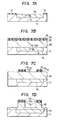
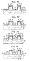
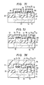
- Figs. 7A - 7R show one example of a manufacturing process for realizing the semiconductor device of the present invention, and illustrate the situations before the structure of Figs. 4 - 6 is formed. Hereunder, the producing steps will be explained in accordance with the figures.
- Fig. 7A A p-type semiconductor substrate 11 is prepared. Although an n-type substrate may be employed, impurities to be mentioned below must have the opposite conductivity types in that case. Unlike the substrate used as an electric conductor, a substrate in a broad sense in the form in which a conductor is placed on an insulator may well be employed. It is represented by SOI (Silicon on Insulator), SOS (Silicon on Sapphire) ' or the like.
- the inventors selected as the substrate, one containing an impurity of the p-type and having an impurity concentration of 5 x 10 14 cm -3
- the substrate is thermally oxidized to form a thin silicon oxide film 71 on the surface thereof.
- the inventors obtained the silicon oxide film 71 of 600 nm by performing a heat treatment at 1000 °C for 150 minutes.
- an opening for forming an n + -type buried layer 14 is provided in the silicon oxide film 71 by employing photolithography as in the prior art.
- the n + -type buried layer 14 having a desired concentration is provided through the opening.
- Fig. 7B The silicon oxide film 71 is subsequently removed to expose the substrate surface, whereupon an n-type single crystal layer 15 is formed by the epitaxial growth.
- the epitaxial layer 15 can be formed to a desired thickness, depending upon a period of time, a temperature etc. for or during the growth.
- the inventors obtained the epitaxial grown layer 15 of 1 pm.
- the oxide film 72 may well be formed by deposition.
- a silicon nitride film 73 is formed by deposition. Further, a silicon oxide film 74 is formed by deposition.
- the inventors formed the three-layer film consisting of the oxide film 72, nitride film 73 and oxide film 74 which were 50 nm, 120 nm and 900 nm thick respectively.
- Fig. 7C The whole surface is coated with a photoresist which is then patterned, and parts of the three-layer film 72, 73, 74 are removed using the photoresist as a mask. Thereafter, the photoresist is removed.
- Fig. 7D Subsequently, using the three-layer film as a mask, the epitaxial grown layer is etched to form convex regions. Since anisotropic dry etching is used for the formation, side etching scarcely arises.
- Fig. 7E A thermal oxide film 75 is formed again. It may well be formed by deposition. In this case, however, the shape is somewhat different. Further, a silicon nitride film 76 is formed thereon by deposition. The inventors formed the silicon oxide film and the silicon nitride film which were 50 nm and 120 nm thick respectively.
- Fig. 7F Subsequently, the resultant structure is etched by anisotropic dry etching so as to leave the silicon nitride film 76 on only the side surfaces of the convex regions. Since the anisotropic dry etching is used, this step does not require any photo-mask for the etching.
- Fig. 7G Subsequently, using the silicon nitride film 76 as a mask, thermal oxidation is performed to form a thick oxide film 22.
- the inventors formed the oxide film of 700 nm.
- Fig. 7H Subsequently, the silicon nitride film . 76 is removed, and further, the silicon oxide film 75 is removed. In removing the silicon oxide film, it is covered with a resist as a photo-mask in order that the oxide films may be left at the parts 61 of the side surfaces of the convex region as shown in Fig. 4. Therefore, the silicon oxide films 61 at the covered parts are not removed.
- Fig. 71 Polycrystalline silicon 21 is deposited on the whole surface, and further, a silicon oxide film 761 is formed by deposition.
- the inventors deposited the polycrystalline silicon in two operations, in each of which it was deposited by 350 nm, to a total thickness of 700 nm, and formed the silicon oxide film by 200 nm.
- Fig. 7J The whole surface is coated with a resist 77, and that part of the resist which is somewhat larger than the convex regions is removed by a photo-mask step.
- the inventors removed the resist in the part which was 1 pm outside one side of each convex region.
- Fig. 7K A photoresist 78 separate from the photoresist 77 is applied to the whole area, and its surface is flattened.
- F i g. 7L Sputter etching is performed in an 0 2 atmosphere, to uniformly remove the photoresist 78 until the oxide film 76 is exposed.
- Fig. 7M The exposed oxide film is removed by wet etching, and the exposed parts of the polycrystalline silicon layer are removed by dry etching.
- Fig. 7N The photoresist layers 77, 78 and the oxide film 761 are removed.
- Fig. 70 A silicon oxide film 79 is formed on the surface of the polycrystalline silicon 21 by thermal oxidation, and a silicon nitride film 80 is deposited on the whole surface. Thereafter, parts of the silicon nitride film and the silicon oxide film are selectively removed by photo-mask steps.
- the polycrystalline silicon layer 21 is etched by dry etching so as to reduce its thickness. This step is performed in order to flatten the surface of the element later, but it may well be omitted.
- Fig. 7P Using the silicon nitride film 80 as a mask, the polycrystalline silicon is selectively oxidized to form an oxide film 51. Thereafter, the silicon nitride film 80 is removed, and the polycrystalline silicon is doped with boron by ion implantation.
- Fig. 7Q The silicon oxide films 74 and 79 are removed.
- Fig. 7R Using the silicon nitride film 73 as a mask, the surface of the polycrystalline silicon layer is oxidized to form a silicon oxide film 81. During this thermal step, the boron having been implanted by the step of Fig. 7P diffuses into the polycrystalline layer 15, so that the p-type regions 12 and 13 are formed.
- the diffusion windows of the p-type regions are determined by the selective etching of the side wall oxide films 75 having been performed in Fig. 7H.-Thereafter, the silicon nitride film 73 is removed.
- a metal such as aluminum (Al) is deposited, and 4 is photo-etched into a desired pattern. It forms an emitter electrode 17E, a collector electrode 17C and a base electrode 17B.
- Examples of the metal other than the aforementioned aluminum are tungsten (W), titanium (Ti) and their compounds with silicon (silicides).
- a passivation film for protection is further formed.
- Figs. 8 and 9 show the base length-dependence of a collector saturation current, and Fig. 9 that of a base saturation current.
- the base length L is equal to the etching width of the side wall oxide films shown in Fig. 4.
- the currents flowing through the device are substantially proportional to L as illustrated in Figs. 8 and 9, and it is understood that the operation is performed stably and precisely.
- the device of the present invention becomes smaller to about 1/3 as compared with the prior-art semiconductor device in Fig. 1 and to about 1/5 as compared with the semiconductor device in Fig. 2, and it has the structure suited to s microminiaturization.
- Fig. 10 is a sectional structural view showing the second embodiment of the semiconductor device of the present invention.
- the bipolar transistor of the present invention indicated by the embodiment has an n + - type layer 105 on the surface of an n-type convex region 15 (including regions 12 and 13) and is provided with a base electrode 17B on the surface of the n -type layer. Therefore, a buried layer does not exist between the real base region and the base electrode. This brings forth the effect that the device is not affected by the state of the buried layer, so the dispersion of a collector current is avoided.
- the dispersion of the voltage between the base and the emitter of the transistor is minimized, and the element having stable characteristics can be provided.
- the dispersion of the collector current of a transistor is determined by the dispersion of a voltage applied to the transistor.
- a voltage V B to be applied to the real base of the lateral p-n-p transistor is obtained in such a way that a voltage drop AV B in the buried layer extending from the base electrode to the real base region is subtracted from the voltage V B ' applied to the base electrode.
- R denotes the resistance (10 2 -10 3 ⁇ ) of the buried layer
- I B the current flowing through the buried layer.
- a base electrode is disposed directly over a real base region, whereby a voltage to be applied to the base electrode is equalized. That is, since a base current flows to the electrode portion directly without passing a buried layer, a voltage drop across the buried layer forming the cause of a dispersion is not involved.
- Fig. 11 is a sectional view showing a third embodiment of the present invention.
- the first embodiment is employed for a lateral transistor portion, while a vertical transistor portion has a p +- type region 101 lying in direct contact with p-type regions 43 and is connected with the lateral transistor by a polycrystalline silicon layer 21C.
- an injector is led out by an electrode 17I through a polycrystalline silicon layer 21C, and a base by an electrode 17B through the polycrystalline silicon layer '21C.
- the ground is led out by an electrode 17G, and a collector by an electrode 17C.
- the ground terminal 17G of the I 2 L circuit exists on the surface of the active region of the lateral transistor. Therefore, even when the I 2 L circuit of Fig. 11 is applied to a large-scale integrated circuit, the dispersion of the injector currents of the individual 1 2 L circuits is minimized, along with the effect of microminiaturization.
- Embodiment 1 This embodiment is obtained by combining Embodiment 1 with Embodiment 2 or 3 described before.
- the base length is precisely controlled by the insulator film 61. Besides, since the base lead-out electrode is disposed directly over the base region, the voltage drop attributed to the resistance of the buried layer is not involved. Therefore, the base potential can be rendered constant without being influenced by the length of the buried layer.
Landscapes
- Bipolar Transistors (AREA)
Applications Claiming Priority (2)
| Application Number | Priority Date | Filing Date | Title |
|---|---|---|---|
| JP25029/84 | 1984-02-15 | ||
| JP59025029A JPH0618198B2 (ja) | 1984-02-15 | 1984-02-15 | 半導体装置 |
Publications (3)
| Publication Number | Publication Date |
|---|---|
| EP0152116A2 true EP0152116A2 (fr) | 1985-08-21 |
| EP0152116A3 EP0152116A3 (en) | 1986-12-30 |
| EP0152116B1 EP0152116B1 (fr) | 1991-01-23 |
Family
ID=12154481
Family Applications (1)
| Application Number | Title | Priority Date | Filing Date |
|---|---|---|---|
| EP85101688A Expired EP0152116B1 (fr) | 1984-02-15 | 1985-02-15 | Transistor bipolaire latéral et son procédé de fabrication |
Country Status (4)
| Country | Link |
|---|---|
| US (1) | US4769687A (fr) |
| EP (1) | EP0152116B1 (fr) |
| JP (1) | JPH0618198B2 (fr) |
| DE (1) | DE3581417D1 (fr) |
Cited By (3)
| Publication number | Priority date | Publication date | Assignee | Title |
|---|---|---|---|---|
| EP0300514A1 (fr) * | 1987-03-18 | 1989-01-25 | Koninklijke Philips Electronics N.V. | Dispositif semi-conducteur ayant une structure de contact latérale et son procédé de fabrication |
| US5043786A (en) * | 1989-04-13 | 1991-08-27 | International Business Machines Corporation | Lateral transistor and method of making same |
| EP0392954A3 (fr) * | 1989-04-13 | 1992-08-12 | International Business Machines Corporation | Transistor latéral et procédé pour sa fabrication |
Families Citing this family (19)
| Publication number | Priority date | Publication date | Assignee | Title |
|---|---|---|---|---|
| JPS561556A (en) * | 1979-06-18 | 1981-01-09 | Hitachi Ltd | Semiconductor device |
| US6372596B1 (en) * | 1985-01-30 | 2002-04-16 | Texas Instruments Incorporated | Method of making horizontal bipolar transistor with insulated base structure |
| DE3545244A1 (de) * | 1985-12-20 | 1987-06-25 | Licentia Gmbh | Strukturierter halbleiterkoerper |
| JP2503460B2 (ja) * | 1986-12-01 | 1996-06-05 | 三菱電機株式会社 | バイポ−ラトランジスタおよびその製造方法 |
| DE3681291D1 (de) * | 1986-12-18 | 1991-10-10 | Itt Ind Gmbh Deutsche | Kollektorkontakt eines integrierten bipolartransistors. |
| JPS63292673A (ja) * | 1987-05-25 | 1988-11-29 | Nec Corp | 横型バイポ−ラトランジスタ |
| US4860077A (en) * | 1987-09-28 | 1989-08-22 | Motorola, Inc. | Vertical semiconductor device having a sidewall emitter |
| US4939474A (en) * | 1988-08-26 | 1990-07-03 | At&T Bell Laboratories | Semiconductor optical amplifier with shortened gain recovery time |
| GB2230134A (en) * | 1989-04-05 | 1990-10-10 | Philips Nv | A method of manufacturing a semiconductor device |
| US5289024A (en) * | 1990-08-07 | 1994-02-22 | National Semiconductor Corporation | Bipolar transistor with diffusion compensation |
| JP3202460B2 (ja) * | 1993-12-21 | 2001-08-27 | 株式会社東芝 | 半導体装置およびその製造方法 |
| US6232649B1 (en) * | 1994-12-12 | 2001-05-15 | Hyundai Electronics America | Bipolar silicon-on-insulator structure and process |
| DE19741972C1 (de) | 1997-09-23 | 1998-09-17 | Siemens Ag | SOI-Zelle und Verfahren zu deren Herstellung |
| US6853048B1 (en) * | 2000-08-11 | 2005-02-08 | Agere Systems Inc. | Bipolar transistor having an isolation structure located under the base, emitter and collector and a method of manufacture thereof |
| US6864547B2 (en) | 2001-06-15 | 2005-03-08 | Agere Systems Inc. | Semiconductor device having a ghost source/drain region and a method of manufacture therefor |
| US6958518B2 (en) * | 2001-06-15 | 2005-10-25 | Agere Systems Inc. | Semiconductor device having at least one source/drain region formed on an isolation region and a method of manufacture therefor |
| US6809386B2 (en) * | 2002-08-29 | 2004-10-26 | Micron Technology, Inc. | Cascode I/O driver with improved ESD operation |
| US7692483B2 (en) * | 2007-10-10 | 2010-04-06 | Atmel Corporation | Apparatus and method for preventing snap back in integrated circuits |
| US8085604B2 (en) * | 2008-12-12 | 2011-12-27 | Atmel Corporation | Snap-back tolerant integrated circuits |
Family Cites Families (6)
| Publication number | Priority date | Publication date | Assignee | Title |
|---|---|---|---|---|
| US3600651A (en) * | 1969-12-08 | 1971-08-17 | Fairchild Camera Instr Co | Bipolar and field-effect transistor using polycrystalline epitaxial deposited silicon |
| JPS5244186A (en) * | 1975-10-06 | 1977-04-06 | Hitachi Ltd | Semiconductor intergrated circuit device |
| US4333227A (en) * | 1979-11-29 | 1982-06-08 | International Business Machines Corporation | Process for fabricating a self-aligned micrometer bipolar transistor device |
| US4338138A (en) * | 1980-03-03 | 1982-07-06 | International Business Machines Corporation | Process for fabricating a bipolar transistor |
| US4339767A (en) * | 1980-05-05 | 1982-07-13 | International Business Machines Corporation | High performance PNP and NPN transistor structure |
| US4508579A (en) * | 1981-03-30 | 1985-04-02 | International Business Machines Corporation | Lateral device structures using self-aligned fabrication techniques |
-
1984
- 1984-02-15 JP JP59025029A patent/JPH0618198B2/ja not_active Expired - Lifetime
-
1985
- 1985-02-15 EP EP85101688A patent/EP0152116B1/fr not_active Expired
- 1985-02-15 DE DE8585101688T patent/DE3581417D1/de not_active Expired - Lifetime
-
1987
- 1987-04-20 US US07/040,125 patent/US4769687A/en not_active Expired - Fee Related
Cited By (3)
| Publication number | Priority date | Publication date | Assignee | Title |
|---|---|---|---|---|
| EP0300514A1 (fr) * | 1987-03-18 | 1989-01-25 | Koninklijke Philips Electronics N.V. | Dispositif semi-conducteur ayant une structure de contact latérale et son procédé de fabrication |
| US5043786A (en) * | 1989-04-13 | 1991-08-27 | International Business Machines Corporation | Lateral transistor and method of making same |
| EP0392954A3 (fr) * | 1989-04-13 | 1992-08-12 | International Business Machines Corporation | Transistor latéral et procédé pour sa fabrication |
Also Published As
| Publication number | Publication date |
|---|---|
| EP0152116B1 (fr) | 1991-01-23 |
| EP0152116A3 (en) | 1986-12-30 |
| JPS60170257A (ja) | 1985-09-03 |
| JPH0618198B2 (ja) | 1994-03-09 |
| DE3581417D1 (de) | 1991-02-28 |
| US4769687A (en) | 1988-09-06 |
Similar Documents
| Publication | Publication Date | Title |
|---|---|---|
| US4769687A (en) | Lateral bipolar transistor and method of producing the same | |
| US4486942A (en) | Method of manufacturing semiconductor integrated circuit BI-MOS device | |
| EP0064466B1 (fr) | Structure logique utilisant des diodes Schottky en silicium polycristallin | |
| US4057894A (en) | Controllably valued resistor | |
| EP0058124B1 (fr) | Matrice de diodes Schottky en silicium polycristallin et procédé de fabrication | |
| US5061645A (en) | Method of manufacturing a bipolar transistor | |
| JPH0123949B2 (fr) | ||
| EP0183624A2 (fr) | Procédé de fabrication de circuits intégrés bipolaires analogiques à haute densité d'intégration à grande vitesse | |
| EP0030147B1 (fr) | Procédé de fabrication d'un circuit intégré à semi-conducteur | |
| EP0078220B1 (fr) | Interférences de silicium polycristallin pour transistors bipolaires en circuit flip-flop | |
| US4835588A (en) | Transistor | |
| US4584594A (en) | Logic structure utilizing polycrystalline silicon Schottky diodes | |
| US4631568A (en) | Bipolar transistor construction | |
| US4949151A (en) | Bipolar transistor having side wall base and collector contacts | |
| EP0264309B1 (fr) | Shunt de base auto-aligné pour un transistor | |
| EP0032016B1 (fr) | Procédé de fabrication d'un dispositif semiconducteur | |
| US5317168A (en) | Superconducting field effect transistor | |
| JPH05343413A (ja) | バイポーラトランジスタとその製造方法 | |
| JPS6025254A (ja) | 集積回路の製造方法 | |
| KR910009740B1 (ko) | 산화막을 이용하여 자기 정합된 바이폴라 트랜지스터의 제조방법 | |
| JPH04291926A (ja) | 半導体装置とその製造方法 | |
| JPH0195555A (ja) | バイポーラ型半導体集積回路装置の製造方法 | |
| JPS58107645A (ja) | 半導体装置の製法 | |
| JPS6022828B2 (ja) | 半導体装置の製造方法 | |
| JPH0361343B2 (fr) |
Legal Events
| Date | Code | Title | Description |
|---|---|---|---|
| PUAI | Public reference made under article 153(3) epc to a published international application that has entered the european phase |
Free format text: ORIGINAL CODE: 0009012 |
|
| AK | Designated contracting states |
Designated state(s): DE FR IT |
|
| PUAL | Search report despatched |
Free format text: ORIGINAL CODE: 0009013 |
|
| AK | Designated contracting states |
Kind code of ref document: A3 Designated state(s): DE FR IT |
|
| 17P | Request for examination filed |
Effective date: 19870108 |
|
| 17Q | First examination report despatched |
Effective date: 19880718 |
|
| RBV | Designated contracting states (corrected) |
Designated state(s): DE |
|
| GRAA | (expected) grant |
Free format text: ORIGINAL CODE: 0009210 |
|
| AK | Designated contracting states |
Kind code of ref document: B1 Designated state(s): DE |
|
| REF | Corresponds to: |
Ref document number: 3581417 Country of ref document: DE Date of ref document: 19910228 |
|
| PLBE | No opposition filed within time limit |
Free format text: ORIGINAL CODE: 0009261 |
|
| STAA | Information on the status of an ep patent application or granted ep patent |
Free format text: STATUS: NO OPPOSITION FILED WITHIN TIME LIMIT |
|
| 26N | No opposition filed | ||
| PGFP | Annual fee paid to national office [announced via postgrant information from national office to epo] |
Ref country code: DE Payment date: 19950428 Year of fee payment: 11 |
|
| PG25 | Lapsed in a contracting state [announced via postgrant information from national office to epo] |
Ref country code: DE Effective date: 19961101 |