EP0164449A2 - Procédé pour fabriquer un dispositif à circuit intégré semi-conducteur comportant un élément du type MISFET - Google Patents
Procédé pour fabriquer un dispositif à circuit intégré semi-conducteur comportant un élément du type MISFET Download PDFInfo
- Publication number
- EP0164449A2 EP0164449A2 EP84116283A EP84116283A EP0164449A2 EP 0164449 A2 EP0164449 A2 EP 0164449A2 EP 84116283 A EP84116283 A EP 84116283A EP 84116283 A EP84116283 A EP 84116283A EP 0164449 A2 EP0164449 A2 EP 0164449A2
- Authority
- EP
- European Patent Office
- Prior art keywords
- gate electrode
- channel
- misfet
- semiconductor region
- semiconductor
- Prior art date
- Legal status (The legal status is an assumption and is not a legal conclusion. Google has not performed a legal analysis and makes no representation as to the accuracy of the status listed.)
- Granted
Links
Images


Classifications
-
- H—ELECTRICITY
- H10—SEMICONDUCTOR DEVICES; ELECTRIC SOLID-STATE DEVICES NOT OTHERWISE PROVIDED FOR
- H10D—INORGANIC ELECTRIC SEMICONDUCTOR DEVICES
- H10D30/00—Field-effect transistors [FET]
- H10D30/01—Manufacture or treatment
- H10D30/021—Manufacture or treatment of FETs having insulated gates [IGFET]
-
- H—ELECTRICITY
- H10—SEMICONDUCTOR DEVICES; ELECTRIC SOLID-STATE DEVICES NOT OTHERWISE PROVIDED FOR
- H10D—INORGANIC ELECTRIC SEMICONDUCTOR DEVICES
- H10D30/00—Field-effect transistors [FET]
- H10D30/60—Insulated-gate field-effect transistors [IGFET]
-
- H—ELECTRICITY
- H10—SEMICONDUCTOR DEVICES; ELECTRIC SOLID-STATE DEVICES NOT OTHERWISE PROVIDED FOR
- H10D—INORGANIC ELECTRIC SEMICONDUCTOR DEVICES
- H10D64/00—Electrodes of devices having potential barriers
- H10D64/01—Manufacture or treatment
- H10D64/021—Manufacture or treatment using multiple gate spacer layers, e.g. bilayered sidewall spacers
-
- H—ELECTRICITY
- H10—SEMICONDUCTOR DEVICES; ELECTRIC SOLID-STATE DEVICES NOT OTHERWISE PROVIDED FOR
- H10D—INORGANIC ELECTRIC SEMICONDUCTOR DEVICES
- H10D64/00—Electrodes of devices having potential barriers
- H10D64/20—Electrodes characterised by their shapes, relative sizes or dispositions
- H10D64/27—Electrodes not carrying the current to be rectified, amplified, oscillated or switched, e.g. gates
- H10D64/311—Gate electrodes for field-effect devices
- H10D64/411—Gate electrodes for field-effect devices for FETs
- H10D64/511—Gate electrodes for field-effect devices for FETs for IGFETs
-
- H—ELECTRICITY
- H10—SEMICONDUCTOR DEVICES; ELECTRIC SOLID-STATE DEVICES NOT OTHERWISE PROVIDED FOR
- H10D—INORGANIC ELECTRIC SEMICONDUCTOR DEVICES
- H10D84/00—Integrated devices formed in or on semiconductor substrates that comprise only semiconducting layers, e.g. on Si wafers or on GaAs-on-Si wafers
- H10D84/01—Manufacture or treatment
- H10D84/0123—Integrating together multiple components covered by H10D12/00 or H10D30/00, e.g. integrating multiple IGBTs
- H10D84/0126—Integrating together multiple components covered by H10D12/00 or H10D30/00, e.g. integrating multiple IGBTs the components including insulated gates, e.g. IGFETs
- H10D84/0165—Integrating together multiple components covered by H10D12/00 or H10D30/00, e.g. integrating multiple IGBTs the components including insulated gates, e.g. IGFETs the components including complementary IGFETs, e.g. CMOS devices
- H10D84/0184—Manufacturing their gate sidewall spacers
-
- H—ELECTRICITY
- H10—SEMICONDUCTOR DEVICES; ELECTRIC SOLID-STATE DEVICES NOT OTHERWISE PROVIDED FOR
- H10D—INORGANIC ELECTRIC SEMICONDUCTOR DEVICES
- H10D84/00—Integrated devices formed in or on semiconductor substrates that comprise only semiconducting layers, e.g. on Si wafers or on GaAs-on-Si wafers
- H10D84/01—Manufacture or treatment
- H10D84/02—Manufacture or treatment characterised by using material-based technologies
- H10D84/03—Manufacture or treatment characterised by using material-based technologies using Group IV technology, e.g. silicon technology or silicon-carbide [SiC] technology
- H10D84/038—Manufacture or treatment characterised by using material-based technologies using Group IV technology, e.g. silicon technology or silicon-carbide [SiC] technology using silicon technology, e.g. SiGe
Definitions
- the present invention relates to a technique which is effective for application to a semiconductor integrated circuit device, hereafter referred to as an "IC", and more particularly, to a fabrication technique which is effective for application to an IC provided with a gate insulated field effect transistor hereafter referred to as a "MISFET".
- IC semiconductor integrated circuit device
- MISFET gate insulated field effect transistor
- an impurity implanted With an annealing treatment after the implantation, an impurity implanted will diffuse below the gate electrode, i.e., into a channel region. As a result,the effective channel length is reduced to induce a short channel effect.
- An object of the present invention is to provide a technique which enables an IC provided with a P-channel MISFET to retain a sufficient effective channel length for the P-channel MISFET thereby to prevent the short channel effect.
- Another object of the present invention is to provide a technique which enables an IC provided with an N-channel MISFET and a P-channel MISFET to retain a sufficient effective channel length for the P-channel MISFET thereby to prevent the short channel effect.
- Still another object of the present invention is to provide a technique which enables an IC provided with an N-channel MISFET and a P-type MISFET to retain sufficient effective channel lengths for the N-channel and P-channel MISFETs thereby to prevent the short channel effect.
- An impurity for forming the drain or source region of the P-channel MISFET is introduced into a semiconductor substrate by using as a mask the gate electrode and side wall spacers formed at both the sides of the gate electrode.
- the source or drain region is sup- pressed from extending around to the region to be formed with the channel.
- the effective channel length can be retained at a sufficient value to prevent the short channel effect of the MISFET.
- the present invention will be described in case it is applied to an IC provided with complementary MISFETs.
- Fig. 1 is a sectional view showing an essential portion of an IC provided with the CMIS for explaining a first embodiment of the present invention.
- reference numeral 1 indicates an N - type semiconductor substrate hereafter referred to as a "substrate", which is made of single crystal of silicon for forming a part of the IC.
- Indicated at numeral 13 is a P -type well region which is formed in a predetermined main surface portion of the substrate 1 to form a part of an N-channel MISFET.
- Indicated at numeral 2 is a field insulating film which is formed on the main surface of the substrate 1 between the regions, which are to be formed with semiconductor elements such as MISFETs, thereby to electrically separate the semiconductor elements.
- Indicated at numeral 3 is a P-type channel stopper region which is formed in the well region 13 below the field insulating film 2 thereby to prevent the leaking phenomena between the semiconductor elements by a parasitic MISFET.
- Indicated at numeral 4 is an insulating film which is formed on the main surface of the substrate 1 in the region to be formed with a MISFET.
- This insulating film 4 is used mainly-as a gate insulating film to form a part of the MISFET.
- a first level conducting layer 5 is formed on the insulating film 4 and used mainly as the gate electrode thereby to form a part of the MISFET.
- insulating side walls, or side wall spacers which are formed on the gate insulating film 4 mainly at both the sides of the first level conducting layer 5 ,i.e., the gate electrode, and in self-alignment with the gate electrode.
- the side walls 6 space farther the paired semiconductor regions, which are used as drain or source regions, to retain a sufficient effective channel length.
- N -type first semiconductor regions the end portions of which at the side of the region to be formed with the channel are formed in the main surface of the substrate 1 at or outside the end portion of the first level conducting layer or the gate electrode 5.
- the semiconductor regions 7 are used as the source region and the drain region thereby to form parts of the MISFET.
- Indicated at numeral 8 are.
- N -type second semiconductor regions which are formed to cover the first semiconductor regions 7.
- the semiconductor regions 8 weaken the electric field, which is established in the vicinity of the boundary between the region to be formed with the channel of the main surface of the substrate 1 and the first semiconductor regions,i.e., the drain and source regions 7 thereby to suppress fluctuations of the threshold voltage of the MISFET by hot carriers.
- the N-channel MISFET is constructed of the substrate 1, the insulating film 4, the first level conducting layer 5 and paired semiconductor regions 7 and 8.
- P t- type third semiconductor regions which are formed in the main surface portion of the substrate 1 at both the sides of the conducting region 5 of the region to be formed with a P-channel MISFET and which are used as the drain region and the source region thereby to form parts of the MI SFE T.
- the P-channel MISFET is constructed of the well region 13, the insulating film 4, the conducting layer 5 and the paired semiconductor regions 15.
- Indicated at numeral 9 is an insulating film which is formed on the substrate 1 in a manner to cover the semiconductor elements thereby to electrically separate mainly the second level conducting layer formed in the upper portion thereof and the semiconductor element.
- the insulating film 9 on the predetermined first semiconductor region 7 is locally removed to form a contact hole 9A. This contact hole 9A is provided to electrically connect the first semiconductor region 7 and the second level conducting layer.
- Indicated at numeral 10 is the second level conducting layer which is electrically connected with the predetermined first semiconductor region 7 through the contact hole 9A and formed to extend on the insulating film 9 thereby to electrically connect the semiconductor elements, for example.
- Indicated at numeral 11 is an insulating film which is formed on the insulating film 9 in a manner to cover the second level conducting layer 10 thereby to electrically-separate the second level conducting layer 10 and a third level conducting layer, although not shown.
- Indicated at numeral 12 is a passivation film which is formed on the insulating film 11 in a manner to cover the third level conducting layer thereby to protect mainly the third level conducting layer against the surrounding atmosphere.
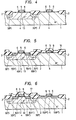
- Figs. 2 to 7 are sectional views showing essential portions of the IC at the respective fabrication steps for l explaining the first embodiment of the present invention.
- the substrate 1 is prepared. And, the P -type well region 13 is formed locally in that substrate 1. Specifically, boron ions are introduced by the ion implantation into the substrate 1 in the state when the surface of the substrate 1 other than the portion to be formed with the well region 13 is covered with a mask such as a silicon nitride film or a resist film. After this, the boron ions thus implanted are thermally diffused to form the well region 13.
- the boron ions are introduced by ion implantation locally into the surface of the well region 13.
- the field insulating film 2 is formed by local oxidization of the substrate 1 using the silicon nitride film as the mask. Simultaneously with this, boron is diffused to form a P-channel stopper region 3.
- the field insulating film 2 is made of a silicon dioxide film having a thickness of 600 to 800 nm.
- the insulating film 4 is formed.
- This insulating film 4 is formed to have a thickness of 30 to 40 nm comprising the silicon dioxide film which is prepared by thermally oxidizing the surface of the substrate 1.
- a tungsten alloy e.g., tungsten silicide layer is formed to have a thickness of about 300 nm by the sputtering method.
- the tungsten silicide layer is patterned by the anisotropic etching technique to form the first level conducting layer 5, as shown in Fig. 2.
- a silicon dioxide film 6A is formed to cover the conducting layer 5.
- This silicon dioxide film 6A is made to have a flat portion thickness of about 300 nm like that of the aforementioned conducting layer 5 by chemical vapor deposition hereafter referred to as "CVD" which can provide a generally even thickness.
- CVD chemical vapor deposition
- the silicon dioxide film 6A is removed from its surface to provide an even thickness by the reactive ion etching technique hereafter referred to as an "RIE".
- RIE reactive ion etching technique
- the side walls 6 which have a width of 0.2 to 0.4 pm.
- the side walls 6 may be formed at a fabrication step similar to the aforementioned one by using a phosphosilicate glass film, which is prepared by the CVD, or a silicon dioxide or nitride film which is prepared by the plasma CVD.
- an impurity for forming the N-channel MISFET is introduced into the well region 13.
- an N-type impurity is introduced into the substrate 1 by using the conducting layer 5 and the side walls 6 as a mask for impurity introduction.
- phosphor ions in a concentration of 0.5 x 10 16 atoms / cm 2 are implanted into the main surface of the substrate 1 through the insulating film 4 by an energy of about 80 KeV.
- arsenic ions in a concentration of about 10 17 to 10 18 atoms/cm 2 are implanted into the main surface of the substrate 1 through the insulating film 4 by an energy of about 50 to 80 KeV.
- the aforementioned impurities are diffused to form the N +- type first semiconductor region 7 and the N -type second semiconductor region 8, as shown in Fig. 5.
- the second semiconductor region 8 is formed to cover the first semiconductor region 7 because the phosphor ions have a higher diffusion velocity than the arsenic ions.
- the first semiconductor regions 7 and the second semiconductor regions 8 are less allowed to extend around to the region to be formed with the channel.
- the source region and the drain region of the MISFET constructed of the first semiconductor region s 7 and the second semiconductor regions 8 can be spaced from each other so that a sufficient effective channel length can be retained to prevent the short channel effect.
- the first semiconductor regicns7 and the second semiconductor regions 8 have their depth differences (xj) as small as 0.1 to 0.2 pm, because their depths are determined by the diffusion velocities of the impurities. As a result, mutual conductance during the operation of the MISFET can be prevented from falling off, thereby speeding up the operation of the IC.
- the region formed with the N-channel MISFET i.e., the well region 13 is covered with a mask such as a silicon nitride film 17.
- a mask such as a silicon nitride film 17.
- an impurity for forming the P-channel MISFET is introduced into the substrate 1.
- a P-type impurity such as boron (B) is introduced into the main surface of the substrate 1 through the insulating film 4 by using ion implantation.
- the P -type source and drain regions 15 are formed, as shown in Fig. 6.
- the diffusion velocity of the boron ions for forming the P -type semiconductor regions 15 is higher than that the phosphor ions for forming the second semiconductor regions 8. As a result, the P-channel MISFET is liable to induce the short channel effect.
- the conducting layer 5 and the side walls 6 are used as the mask for the impurity introduction even in the P-channel MISFET, like in the aforementioned N-channel MISFET.
- the third semiconductor regiors15 can be less allowed to extend around to the portion to be formed with the channel, thereby to retain sufficient effective channel length of the P-channel MISFET so that the short channel effect can be prevented.
- the insulating film 9 is formed to cover the conducting layer 5.
- This insulating film 9 is formed of a phosphosilicate glass film to have a thickness of 500 to 600 nm by the CVD, for example. Moreover, the insulating film 9 on the predetermined first semiconductor region 7 is locally removed to form the contact hole 9A.
- the second level conducting layer 10 is formed on the insulating film 9 such that it is electrically connected with the first conductor region 7 through the contact hole 9A.
- This second level conducting layer 10 is formed of a conducting layer, which is made of aluminum or its alloy by the sputtering method, for example, to have a thickness of 300 to 400 nm.
- the insulating film 11 is formed.
- This insulating film 11 is formed of a phosphosilicate glass film, which is prepared by the CVD, to have a thickness of about 800 to 900 nm.
- the passivation film 12 is formed, as shown in Fig. 1.
- This passivation film 12 is formed of the phosphosilicate glass, which is prepared by the CVD, for example, to have a thickness of about 800 to 900 nm.
- the IC according to the first embodiment is completed by the series of fabricating steps thus far described.
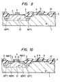
- Fig. 8 is a sectional view showing an essential portion of the IC provided with a CMIS for explaining a second embodiment of the present invention.
- the N-channel MISFET adopts an LDD (i.e., lightly doped drain) structure.
- LDD lightly doped drain
- This LDD structure is disclosed in IEEE TRANSACTIONS ON ELECTRON DEVICES, VOL.ED-29, No. 4, pp. 590 - pp. 596 by Paul J. Tsang et al. According to this LDD structure, it is possible to prevent fluctuations of the threshold voltage by hot carriers.
- the source and drain regiorsof the N-channel MISFET of Fig. 8 are formed of fourth semiconductor regiors 18 having a high impurity concentration (of N + -type), and fifth semiconductor regions19 which have a lower impurity concentration (of N -type) than the former and which are formed between the fourth semiconductor regiorsl8 and a region to be formed with a channel.
- P -type well region 13 the field insulating film 2, the channel stopper region 3, the gate insulating film 4 and the gate electrode 5 are formed at steps similar to those of the first embodiment.
- the region to be formed with the P-channel MISFET is covered with a mask such as a resist film 20.
- a mask such as a resist film 20.
- an N-type impurity such as phosphor is introduced into the well region 13 by the ion implantation using the gate electrode 5 as the mask.
- the side walls 6 made of a silicon dioxide film are formed in accordance with the steps shown in Figs. 3 and 4.
- the region to be formed with the P-channel MISFET is covered again with a mask such as a silicon nitride film 21.
- a mask such as a silicon nitride film 21.
- an N-type impurity such as arsenic is introduced into the well region 13 by the ion implantation using the gate electrode 5 and the side walls 6 as the mask.
- the phosphor and arsenic thus introduced are thermally diffused to form the N -type semiconductor regions19 and the N -type semiconductor regions18, as shown in Fig. 10.
- the P-channel MISFET is formed at the same step as in the first embodiment.
- the impurities are introduced by forming the side walls at both the sides of the gate electrode so that the source region and the drain region can be prevented from extending around to the region to be formed with the channel.
- the effective channel length of the P-channel MISFET can be retained at a sufficient level.
- the MISFETs can have their sizes reduced to improve the integration of the IC.
- the introduction of those impurities is performed by the ion implantation but may be effected by the thermal diffusion to form the source or drain regions of the MISFETs.
- the present invention can also be applied to the IC which is formed with an N-channel MISFET in a P-type semiconductor substrate and a P-channel MISFET in an N-type well region.
Landscapes
- Metal-Oxide And Bipolar Metal-Oxide Semiconductor Integrated Circuits (AREA)
- Insulated Gate Type Field-Effect Transistor (AREA)
- Electrodes Of Semiconductors (AREA)
Applications Claiming Priority (2)
| Application Number | Priority Date | Filing Date | Title |
|---|---|---|---|
| JP59049042A JPH0693494B2 (ja) | 1984-03-16 | 1984-03-16 | 半導体集積回路装置の製造方法 |
| JP49042/84 | 1984-03-16 |
Publications (3)
| Publication Number | Publication Date |
|---|---|
| EP0164449A2 true EP0164449A2 (fr) | 1985-12-18 |
| EP0164449A3 EP0164449A3 (en) | 1987-01-07 |
| EP0164449B1 EP0164449B1 (fr) | 1990-10-31 |
Family
ID=12820022
Family Applications (1)
| Application Number | Title | Priority Date | Filing Date |
|---|---|---|---|
| EP84116283A Expired - Lifetime EP0164449B1 (fr) | 1984-03-16 | 1984-12-24 | Procédé pour fabriquer un dispositif à circuit intégré semi-conducteur comportant un élément du type MISFET |
Country Status (7)
| Country | Link |
|---|---|
| US (1) | US4637124A (fr) |
| EP (1) | EP0164449B1 (fr) |
| JP (1) | JPH0693494B2 (fr) |
| KR (1) | KR850006656A (fr) |
| DE (1) | DE3483531D1 (fr) |
| HK (1) | HK20993A (fr) |
| SG (1) | SG102592G (fr) |
Cited By (7)
| Publication number | Priority date | Publication date | Assignee | Title |
|---|---|---|---|---|
| EP0166167A3 (en) * | 1984-05-16 | 1987-01-28 | Hitachi, Ltd. | Semiconductor device comprising misfets and a process for manufacturing the same |
| EP0206481A3 (fr) * | 1985-05-07 | 1987-08-26 | Hitachi, Ltd. | Dispositif semi-conducteur comprenant des connexions multi-couches |
| EP0228815A3 (en) * | 1985-12-04 | 1988-09-07 | Advanced Micro Devices, Inc. | Field effect transistors |
| EP0322665A3 (en) * | 1987-12-21 | 1990-02-14 | Sgs-Thomson Microelectronics S.R.L. | Process for manufacturing cmos integrated devices with reduced gate lengths |
| EP0405293A1 (fr) * | 1989-06-27 | 1991-01-02 | National Semiconductor Corporation | ProcÀ©dé CMOS compatible avec les siliciures utilisant un masque d'implantation formé par oxydation différentielle |
| DE4112044A1 (de) * | 1990-05-30 | 1991-12-05 | Mitsubishi Electric Corp | Halbleitereinrichtung mit wenigstens zwei feldeffekttransistoren und herstellungsverfahren fuer diese |
| GB2314973A (en) * | 1996-06-29 | 1998-01-14 | Hyundai Electronics Ind | Semiconductor device with low threshold voltage |
Families Citing this family (23)
| Publication number | Priority date | Publication date | Assignee | Title |
|---|---|---|---|---|
| US5610089A (en) * | 1983-12-26 | 1997-03-11 | Hitachi, Ltd. | Method of fabrication of semiconductor integrated circuit device |
| JPH0695563B2 (ja) * | 1985-02-01 | 1994-11-24 | 株式会社日立製作所 | 半導体装置 |
| US5276346A (en) * | 1983-12-26 | 1994-01-04 | Hitachi, Ltd. | Semiconductor integrated circuit device having protective/output elements and internal circuits |
| US4843023A (en) * | 1985-09-25 | 1989-06-27 | Hewlett-Packard Company | Process for forming lightly-doped-drain (LDD) without extra masking steps |
| US4735911A (en) * | 1985-12-17 | 1988-04-05 | Siemens Aktiengesellschaft | Process for the simultaneous production of bipolar and complementary MOS transistors on a common silicon substrate |
| JPH0831602B2 (ja) * | 1986-06-30 | 1996-03-27 | 沖電気工業株式会社 | Mis型電界効果トランジスタの製造方法 |
| US5215936A (en) * | 1986-10-09 | 1993-06-01 | Kabushiki Kaisha Toshiba | Method of fabricating a semiconductor device having a lightly-doped drain structure |
| US4978628A (en) * | 1986-11-19 | 1990-12-18 | Teledyne Industries, Inc. | Drail-well/extension high voltage MOS transistor structure and method of fabrication |
| US4801555A (en) * | 1987-01-14 | 1989-01-31 | Motorola, Inc. | Double-implant process for forming graded source/drain regions |
| JPS63302565A (ja) * | 1987-06-02 | 1988-12-09 | Sanyo Electric Co Ltd | Mos半導体装置の製造方法 |
| JPS63302566A (ja) * | 1987-06-02 | 1988-12-09 | Sanyo Electric Co Ltd | Mos半導体装置の製造方法 |
| JPS63302567A (ja) * | 1987-06-02 | 1988-12-09 | Sanyo Electric Co Ltd | Mos半導体装置の製造方法 |
| JPS63302568A (ja) * | 1987-06-02 | 1988-12-09 | Sanyo Electric Co Ltd | Mos半導体装置の製造方法 |
| US4771014A (en) * | 1987-09-18 | 1988-09-13 | Sgs-Thomson Microelectronics, Inc. | Process for manufacturing LDD CMOS devices |
| JPH01175260A (ja) * | 1987-12-29 | 1989-07-11 | Nec Corp | 絶縁ゲート電界効果トランジスタの製造方法 |
| JPH01189962A (ja) * | 1988-01-26 | 1989-07-31 | Seiko Instr & Electron Ltd | 半導体集積回路装置の製造方法 |
| US5075249A (en) * | 1988-04-04 | 1991-12-24 | Fujitsu Limited | Method of making a bic memory cell having contact openings with straight sidewalls and sharp-edge rims |
| US5006477A (en) * | 1988-11-25 | 1991-04-09 | Hughes Aircraft Company | Method of making a latch up free, high voltage, CMOS bulk process for sub-half micron devices |
| USH986H (en) | 1989-06-09 | 1991-11-05 | International Business Machines Corporation | Field effect-transistor with asymmetrical structure |
| US5021353A (en) * | 1990-02-26 | 1991-06-04 | Micron Technology, Inc. | Split-polysilicon CMOS process incorporating self-aligned silicidation of conductive regions |
| US5943565A (en) * | 1997-09-05 | 1999-08-24 | Advanced Micro Devices, Inc. | CMOS processing employing separate spacers for independently optimized transistor performance |
| US7880173B2 (en) * | 2002-06-28 | 2011-02-01 | National Institute Of Advanced Industrial Science And Technology | Semiconductor device and method of manufacturing same |
| US9293577B2 (en) * | 2010-03-30 | 2016-03-22 | Volterra Semiconductor LLC | LDMOS with no reverse recovery |
Family Cites Families (9)
| Publication number | Priority date | Publication date | Assignee | Title |
|---|---|---|---|---|
| US4356623A (en) * | 1980-09-15 | 1982-11-02 | Texas Instruments Incorporated | Fabrication of submicron semiconductor devices |
| US4366613A (en) * | 1980-12-17 | 1983-01-04 | Ibm Corporation | Method of fabricating an MOS dynamic RAM with lightly doped drain |
| JPS5879766A (ja) * | 1981-11-06 | 1983-05-13 | Nec Corp | Mos型半導体装置の製造法 |
| JPS58159345A (ja) * | 1982-03-18 | 1983-09-21 | Toshiba Corp | 半導体装置及びその製造方法 |
| JPS58201362A (ja) * | 1982-05-20 | 1983-11-24 | Toshiba Corp | 半導体装置の製造方法 |
| JPS5952849A (ja) * | 1982-09-20 | 1984-03-27 | Fujitsu Ltd | 半導体装置の製造方法 |
| US4536944A (en) * | 1982-12-29 | 1985-08-27 | International Business Machines Corporation | Method of making ROM/PLA semiconductor device by late stage personalization |
| JPS59138379A (ja) * | 1983-01-27 | 1984-08-08 | Toshiba Corp | 半導体装置の製造方法 |
| DE3314450A1 (de) * | 1983-04-21 | 1984-10-25 | Siemens AG, 1000 Berlin und 8000 München | Verfahren zum herstellen von hochintegrierten komplementaeren mos-feldeffekttransistorschaltungen |
-
1984
- 1984-03-16 JP JP59049042A patent/JPH0693494B2/ja not_active Expired - Lifetime
- 1984-12-24 DE DE8484116283T patent/DE3483531D1/de not_active Expired - Lifetime
- 1984-12-24 EP EP84116283A patent/EP0164449B1/fr not_active Expired - Lifetime
-
1985
- 1985-02-25 KR KR1019850001158A patent/KR850006656A/ko not_active Ceased
- 1985-03-18 US US06/712,760 patent/US4637124A/en not_active Expired - Lifetime
-
1992
- 1992-10-07 SG SG1025/92A patent/SG102592G/en unknown
-
1993
- 1993-03-11 HK HK209/93A patent/HK20993A/en not_active IP Right Cessation
Cited By (10)
| Publication number | Priority date | Publication date | Assignee | Title |
|---|---|---|---|---|
| EP0166167A3 (en) * | 1984-05-16 | 1987-01-28 | Hitachi, Ltd. | Semiconductor device comprising misfets and a process for manufacturing the same |
| EP0206481A3 (fr) * | 1985-05-07 | 1987-08-26 | Hitachi, Ltd. | Dispositif semi-conducteur comprenant des connexions multi-couches |
| EP0228815A3 (en) * | 1985-12-04 | 1988-09-07 | Advanced Micro Devices, Inc. | Field effect transistors |
| EP0322665A3 (en) * | 1987-12-21 | 1990-02-14 | Sgs-Thomson Microelectronics S.R.L. | Process for manufacturing cmos integrated devices with reduced gate lengths |
| EP0405293A1 (fr) * | 1989-06-27 | 1991-01-02 | National Semiconductor Corporation | ProcÀ©dé CMOS compatible avec les siliciures utilisant un masque d'implantation formé par oxydation différentielle |
| US5399513A (en) * | 1989-06-27 | 1995-03-21 | National Semiconductor Corporation | Salicide compatible CMOS process with a differential oxide implant mask |
| DE4112044A1 (de) * | 1990-05-30 | 1991-12-05 | Mitsubishi Electric Corp | Halbleitereinrichtung mit wenigstens zwei feldeffekttransistoren und herstellungsverfahren fuer diese |
| US5212542A (en) * | 1990-05-30 | 1993-05-18 | Mitsubishi Denki Kabushiki Kaisha | Semiconductor device having at least two field effect transistors and method of manufacturing the same |
| GB2314973A (en) * | 1996-06-29 | 1998-01-14 | Hyundai Electronics Ind | Semiconductor device with low threshold voltage |
| GB2314973B (en) * | 1996-06-29 | 2001-09-19 | Hyundai Electronics Ind | Semiconductor device and its manufacturing method |
Also Published As
| Publication number | Publication date |
|---|---|
| HK20993A (en) | 1993-03-19 |
| EP0164449A3 (en) | 1987-01-07 |
| JPS60194568A (ja) | 1985-10-03 |
| EP0164449B1 (fr) | 1990-10-31 |
| DE3483531D1 (de) | 1990-12-06 |
| JPH0693494B2 (ja) | 1994-11-16 |
| US4637124A (en) | 1987-01-20 |
| KR850006656A (ko) | 1985-10-14 |
| SG102592G (en) | 1992-12-24 |
Similar Documents
| Publication | Publication Date | Title |
|---|---|---|
| EP0164449A2 (fr) | Procédé pour fabriquer un dispositif à circuit intégré semi-conducteur comportant un élément du type MISFET | |
| US6518623B1 (en) | Semiconductor device having a buried-channel MOS structure | |
| US5548143A (en) | Metal oxide semiconductor transistor and a method for manufacturing the same | |
| US6316302B1 (en) | Isotropically etching sidewall spacers to be used for both an NMOS source/drain implant and a PMOS LDD implant | |
| US6046472A (en) | Graded LDD implant process for sub-half-micron MOS devices | |
| US5510279A (en) | Method of fabricating an asymmetric lightly doped drain transistor device | |
| EP0208935B1 (fr) | TEC à canal étroit | |
| KR970000535B1 (ko) | Mos 전계효과 트랜지스터 및 그 회로 제조방법 | |
| EP0166167B1 (fr) | Procédé pour fabriquer un dispositif à semi-conducteur comportant des MISFETs à canal-n et à canal-p | |
| US5552329A (en) | Method of making metal oxide semiconductor transistors | |
| KR0130376B1 (ko) | 반도체소자 제조방법 | |
| US5712503A (en) | Metal oxide semiconductor and method of making the same | |
| EP1280191A2 (fr) | Méthode pour former des régions de source/drain saillantes avec des espaceurs en polysilicium | |
| KR100276744B1 (ko) | Ldd구조를 갖는 반도체 장치와 그 제조방법 | |
| EP0019119A2 (fr) | Procédé de fabrication d'un transistor à effet de champ à canal court et transistor à effet de champ fabriqué selon ce procédé | |
| US6008100A (en) | Metal-oxide semiconductor field effect transistor device fabrication process | |
| US5504024A (en) | Method for fabricating MOS transistors | |
| US4197630A (en) | Method of fabricating MNOS transistors having implanted channels | |
| EP0401577B1 (fr) | Dispositif semi-conducteur métal-oxyde et sa méthode de fabrication | |
| JPH09223797A (ja) | 半導体装置の製造方法 | |
| JPH06268057A (ja) | 半導体装置の製造方法 | |
| JPH08172139A (ja) | 半導体装置製造方法 | |
| KR100415191B1 (ko) | 비대칭형 씨모스 트랜지스터의 제조 방법 | |
| US6207520B1 (en) | Rapid thermal anneal with a gaseous dopant species for formation of lightly doped regions | |
| JPS61139070A (ja) | 半導体装置 |
Legal Events
| Date | Code | Title | Description |
|---|---|---|---|
| PUAI | Public reference made under article 153(3) epc to a published international application that has entered the european phase |
Free format text: ORIGINAL CODE: 0009012 |
|
| 17P | Request for examination filed |
Effective date: 19841224 |
|
| AK | Designated contracting states |
Designated state(s): DE FR GB IT |
|
| PUAL | Search report despatched |
Free format text: ORIGINAL CODE: 0009013 |
|
| AK | Designated contracting states |
Kind code of ref document: A3 Designated state(s): DE FR GB IT |
|
| 17Q | First examination report despatched |
Effective date: 19890119 |
|
| GRAA | (expected) grant |
Free format text: ORIGINAL CODE: 0009210 |
|
| AK | Designated contracting states |
Kind code of ref document: B1 Designated state(s): DE FR GB IT |
|
| REF | Corresponds to: |
Ref document number: 3483531 Country of ref document: DE Date of ref document: 19901206 |
|
| ITTA | It: last paid annual fee | ||
| ET | Fr: translation filed | ||
| ITF | It: translation for a ep patent filed | ||
| PLBI | Opposition filed |
Free format text: ORIGINAL CODE: 0009260 |
|
| 26 | Opposition filed |
Opponent name: TELEFUNKEN ELECTRONIC GMBH Effective date: 19910719 |
|
| PLBN | Opposition rejected |
Free format text: ORIGINAL CODE: 0009273 |
|
| STAA | Information on the status of an ep patent application or granted ep patent |
Free format text: STATUS: OPPOSITION REJECTED |
|
| 27O | Opposition rejected |
Effective date: 19920905 |
|
| PGFP | Annual fee paid to national office [announced via postgrant information from national office to epo] |
Ref country code: GB Payment date: 19980930 Year of fee payment: 15 |
|
| PGFP | Annual fee paid to national office [announced via postgrant information from national office to epo] |
Ref country code: FR Payment date: 19981217 Year of fee payment: 15 |
|
| PGFP | Annual fee paid to national office [announced via postgrant information from national office to epo] |
Ref country code: DE Payment date: 19990223 Year of fee payment: 15 |
|
| PG25 | Lapsed in a contracting state [announced via postgrant information from national office to epo] |
Ref country code: GB Free format text: LAPSE BECAUSE OF NON-PAYMENT OF DUE FEES Effective date: 19991224 |
|
| GBPC | Gb: european patent ceased through non-payment of renewal fee |
Effective date: 19991224 |
|
| PG25 | Lapsed in a contracting state [announced via postgrant information from national office to epo] |
Ref country code: FR Free format text: LAPSE BECAUSE OF NON-PAYMENT OF DUE FEES Effective date: 20000831 |
|
| PG25 | Lapsed in a contracting state [announced via postgrant information from national office to epo] |
Ref country code: DE Free format text: LAPSE BECAUSE OF NON-PAYMENT OF DUE FEES Effective date: 20001003 |
|
| REG | Reference to a national code |
Ref country code: FR Ref legal event code: ST |