EP0185529A2 - Dynamischer Halbleiterspeicher mit einer statischen Datenspeicherzelle - Google Patents
Dynamischer Halbleiterspeicher mit einer statischen Datenspeicherzelle Download PDFInfo
- Publication number
- EP0185529A2 EP0185529A2 EP85309118A EP85309118A EP0185529A2 EP 0185529 A2 EP0185529 A2 EP 0185529A2 EP 85309118 A EP85309118 A EP 85309118A EP 85309118 A EP85309118 A EP 85309118A EP 0185529 A2 EP0185529 A2 EP 0185529A2
- Authority
- EP
- European Patent Office
- Prior art keywords
- memory cell
- bit lines
- data
- lines
- memory cells
- Prior art date
- Legal status (The legal status is an assumption and is not a legal conclusion. Google has not performed a legal analysis and makes no representation as to the accuracy of the status listed.)
- Granted
Links
Images



Classifications
-
- G—PHYSICS
- G11—INFORMATION STORAGE
- G11C—STATIC STORES
- G11C11/00—Digital stores characterised by the use of particular electric or magnetic storage elements; Storage elements therefor
- G11C11/21—Digital stores characterised by the use of particular electric or magnetic storage elements; Storage elements therefor using electric elements
- G11C11/34—Digital stores characterised by the use of particular electric or magnetic storage elements; Storage elements therefor using electric elements using semiconductor devices
- G11C11/40—Digital stores characterised by the use of particular electric or magnetic storage elements; Storage elements therefor using electric elements using semiconductor devices using transistors
-
- G—PHYSICS
- G11—INFORMATION STORAGE
- G11C—STATIC STORES
- G11C7/00—Arrangements for writing information into, or reading information out from, a digital store
- G11C7/10—Input/output [I/O] data interface arrangements, e.g. I/O data control circuits, I/O data buffers
- G11C7/1051—Data output circuits, e.g. read-out amplifiers, data output buffers, data output registers, data output level conversion circuits
- G11C7/106—Data output latches
-
- G—PHYSICS
- G11—INFORMATION STORAGE
- G11C—STATIC STORES
- G11C11/00—Digital stores characterised by the use of particular electric or magnetic storage elements; Storage elements therefor
- G11C11/005—Digital stores characterised by the use of particular electric or magnetic storage elements; Storage elements therefor comprising combined but independently operative RAM-ROM, RAM-PROM, RAM-EPROM cells
-
- G—PHYSICS
- G11—INFORMATION STORAGE
- G11C—STATIC STORES
- G11C11/00—Digital stores characterised by the use of particular electric or magnetic storage elements; Storage elements therefor
- G11C11/21—Digital stores characterised by the use of particular electric or magnetic storage elements; Storage elements therefor using electric elements
- G11C11/34—Digital stores characterised by the use of particular electric or magnetic storage elements; Storage elements therefor using electric elements using semiconductor devices
- G11C11/40—Digital stores characterised by the use of particular electric or magnetic storage elements; Storage elements therefor using electric elements using semiconductor devices using transistors
- G11C11/401—Digital stores characterised by the use of particular electric or magnetic storage elements; Storage elements therefor using electric elements using semiconductor devices using transistors forming cells needing refreshing or charge regeneration, i.e. dynamic cells
- G11C11/4063—Auxiliary circuits, e.g. for addressing, decoding, driving, writing, sensing or timing
- G11C11/407—Auxiliary circuits, e.g. for addressing, decoding, driving, writing, sensing or timing for memory cells of the field-effect type
- G11C11/409—Read-write [R-W] circuits
- G11C11/4096—Input/output [I/O] data management or control circuits, e.g. reading or writing circuits, I/O drivers or bit-line switches
-
- G—PHYSICS
- G11—INFORMATION STORAGE
- G11C—STATIC STORES
- G11C7/00—Arrangements for writing information into, or reading information out from, a digital store
- G11C7/10—Input/output [I/O] data interface arrangements, e.g. I/O data control circuits, I/O data buffers
- G11C7/1051—Data output circuits, e.g. read-out amplifiers, data output buffers, data output registers, data output level conversion circuits
-
- G—PHYSICS
- G11—INFORMATION STORAGE
- G11C—STATIC STORES
- G11C7/00—Arrangements for writing information into, or reading information out from, a digital store
- G11C7/10—Input/output [I/O] data interface arrangements, e.g. I/O data control circuits, I/O data buffers
- G11C7/1078—Data input circuits, e.g. write amplifiers, data input buffers, data input registers, data input level conversion circuits
-
- G—PHYSICS
- G11—INFORMATION STORAGE
- G11C—STATIC STORES
- G11C7/00—Arrangements for writing information into, or reading information out from, a digital store
- G11C7/10—Input/output [I/O] data interface arrangements, e.g. I/O data control circuits, I/O data buffers
- G11C7/1078—Data input circuits, e.g. write amplifiers, data input buffers, data input registers, data input level conversion circuits
- G11C7/1087—Data input latches
Definitions
- the present invention relates to a semiconductor memory device, and, more particularly, to a dynamic random access memory wherein each memory cell comprises one transistor and one capacitor, and data can be randomly read/written.
- dRAM dynamic random access memory
- a page mode dRAM has been proposed.
- a dRAM of this type unlike a conventional memory wherein row and column address lines (i.e., word and bit lines) must be reset and pre-charged every time selection of one cell is completed, even after a cell is selected, word lines connected to the selected cell are not reset but are continuously activated.
- the readout mode of this dRAM after a desired cell is selected the word line connected thereto is left activated. Therefore, when another desired cell is designated by using only a bit line from the other cells connected to this word line, high-speed selection can be achieved. As a result, the data access speed of the page mode dRAM can be increased to twice that of a normal mode dRAM.
- a dRAM can be driven in a nibble mode.
- cell selection is performed so that four cells (i.e., 4 bits) connected to intersections between two adjacent word lines and two adjacent bit lines are used as one unit.
- the two word lines are continuously activated.
- a desired cell is designated by a shiftregister from the designated four cells.
- the two bit lines need not be pre-charged in order to designate one desired cell from four cells. Therefore, the data access speed of the dRAM can be further improved as compared to the page mode dRAM.
- the pre-charge operation cannot be completely eliminated from all the operation modes.
- presence of a pre-charge period means degradation in improvement in data access speed. This is because during the pre-charge period data accessing cannot be performed, with the pre-charge time undesirably protracting the time needed for data accessing. Therefore, even though the above method is used, data access speed of a dRAM is limited and cannot cope with demand for further improvement.
- the page mode dRAM requires a pre-charge operation when data accessing is shifted from one word line to another word line, a pre-charge operation that takes the same period of time as in a normal mode dRAM.
- an object of the present invention to provide a new and improved dynamic semiconductor memory device which can read/write data during a pre-charge period; therefore greatly improving data access speed.
- a plurality of bit lines are formed parallel to each other on a substrate.
- a plurality of memory cell word lines are provided substantially perpendicular to the bit lines.
- a memory cell is provided at each intersection between the bit and word lines.
- Static auxiliary memory cells are connected to the bit lines through transfer gates. When a desired word line is selected, the static auxiliary memory cells receive data voltages stored in the memory cells connected to the selected word line and temporarily and statically hold them.
- the data voltages are stored in auxiliary memory cells until another word line is selected. Therefore, during the pre-charge period, arbitrary data in the stored data can be read out or rewritten in the corresponding memory cell. As a result, wasteful standby time in data accessing can be effectively eliminated and operation speed of the dRAM improved.
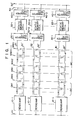
- a dynamic random access memory (to be referred to as a "dRAM” hereinafter) according to one preferred embodiment of the present invention will be described with reference to Figs. 1 and 2 (wherein a chip substrate is omitted from these figures for the sake of simplifying the drawings).
- the dRAM has a so-called folded-bit-line configuration.
- bit line pairs Bl, Bl', B2, B2',..., Bi, Bi',... are formed parallel to each other on a substrate.
- a pair of word lines for dummy cells (to be referred to as “dummy cell word lines” hereinafter) DW1 and DW2 and a plurality of word lines for memory cells (to be referred to as “memory cell word lines” hereinafter) MW1, MW2,..., MW(n-I), MWn run substantially perpendicular to these bit lines B and B'.
- Dummy cells DC are provided at intersections between the bit lines B and B t and the dummy cell word lines DW in a known manner.
- Memory cells MC are provided at intersections between the bit lines B and B' and the memory cell word lines MW in a known manner.
- Each cell comprises a switching transistor and a capacitor.
- Sense-amplifiers 10-1, 10-2,..., 10-i,... are connected to the bit line pairs B1, B1', B2, B2',..., Bi, Bi',... at first ends thereof.
- Static memory cells 20-1, 20-2,..., 20-i are connected to second ends of the bit line pairs B1, B1', B2, B2',..., Bi, Bi',... through corresponding first transfer gate sections 30-1, 30-2,..., 30-i, respectively.
- each static memory cell 20 comprises a latch memory cell and serves as an auxiliary memory cell.
- Each static auxiliary memory cell 20 is connected to an input/output line pair 50 and 50' through corresponding second transfer gate sections 40-1, 40-2,..., 40-i.
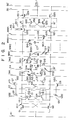
- the sense-amplifier 10-i (to be indicated by "10" hereinafter for the sake of simplicity, something applicable to other components as well) is connected to an ith pair of the bit lines Bi and Bi'.
- the sense-amplifier 10 includes metal oxide semiconductor field effect transistors (MOSFETs) Ql and Q2 and a pull-up circuit 12.
- MOSFETs Ql and Q2 are connected to the bit lines Bi and Bi', respectively.
- the sources of the MOSFETs Ql and Q2 are commonly connected to each other, and are connected to a sense-clock line K1. In these MOSFETs Ql and Q2 the gate of one MOSFET is connected to the drain of the other MOSFET, thereby constituting a driver circuit.
- the pull-up circuit 12 is provided between the bit lines Bi and Bi'.
- the pull-up circuit 12 includes MOSFETs Q3 and Q4 and pull-up capacitors (MOS capacitors) Cl and C2, corresponding thereto in a known manner. More specifically, a series circuit of the capacitor Cl and the FET Q3 is connected between the bit line Bi and a clock line K2, while a series circuit of the capacitor C2 and the FET Q4 is connected between the other bit line Bi' and the clock line K2. In the FETs Q3 and Q4 the gate of one MOSFET is connected to the drain of the other MOSFET.
- MOSFETs Q5 and Q6 are connected to the bit lines Bi and Bi', respectively.
- the drains of the MOSFETs Q5 and Q6 are connected to a power supply voltage Vdd so as to serve as an active pull-up load.
- the gates of the MOSFETs Q5 and Q6 are connected to nodes between the FET-capacitor pairs (i.e., Q3 and Cl; Q4 and C2) in the pull-up circuit 12.
- MOSFETs Q7 and Q8 are provided to switch the gates of the MOSFETs Q5 and Q6 so as to control the pre-charge operation. Therefore, the FET Q7 is connected between the gate of the FET Q5 and the power supply voltage Vdd, while the FET Q8 is connected between the gate of the FET Q6 and the power supply voltage Vdd.
- MOSFETs Q9, Q10 and Qll are provided so as to pre-charge the bit lines Bi and Bi' and to activate the sense-amplifier 10.
- the gates of the FETs Q9, Q10 and Qll are connected in common to a pre-charge clock line K3.
- the clock line K3 is also connected to the gates of the FETs Q7 and Q8.
- the source and drain of the FET Q9 are connected between the bit lines Bi and Bi'.
- the sources of the FETs Q10 and Qll are connected to the bit lines Bi and Bi', respectively, and the drains thereof are connected to the power supply voltage Vdd.
- the dummy cell DC1 is provided at an intersection of the dummy cell word line DW1 and the bit line Bi
- the dummy cell DC2 is provided at an intersection of the dummy cell word line DW2 and the bit line Bi'.
- a switching MOSFET Q12 is connected to the dummy cell word line DW1 and the bit line Bi.
- the data storing capacitor C3 is connected to the source of the MOSFET Q12.
- a switching MOSFET Q13 is connected to the dummy cell word line DW2 and the bit line Bi'.
- the data storing capacitor C4 is connected to the source of the MOSFET Q13.
- the MOSFETs Q12 and Q13 of these dummy cells can be selected by the dummy cell word lines DW.
- the MOSFETs Q12 and Q13 are further connected to the ground potential Vss through MOSFETs Q14 and Q15.
- the gates of the MOSFETs Q14 and Q15 are connected to the dummy cell clock line K4. Therefore, the MOSFETs Q14 and Q15 are simultaneously selected by a dummy cell clock signal supplied onto the clock line.
- the potential at reference terminals (illustrated like free terminals in Fig. 2) of the dummy cell capacitors C3 and C4 is set to be equal to the power supply voltage Vdd, the ground potential Vss, or half of the voltage Vdd (i.e., 1 2 Vdd).
- Fig. 2 illustrates four memory cells MC1, MC2, MC(n-l) and MCn provided at intersections of the four memory cell word lines MWl, MW2, MW(n-l) and MWn with respect to the ith bit line pair Bi and Bi'. More specifically, the memory cell MC1 is provided at the intersection of the memory cell word line MW1 and the bit line Bi, and the memory cell MC2 is provided at the intersection of the memory cell word line MWl and the bit line Bi'.
- the memory cells MC(n-l) and MCn are connected in the same manner as described above.
- Each memory cell MC has a MOSFET and a data storing capacitor, as in a dummy cell.
- the memory cell MC1 comprises a switching MOSFET Q16 connected to the word line MW1 and the bit line Bi, and a data storing capacitor C5 connected to the MOSFET Q16.
- the memory cell MC2 comprises a switching MOSFET Q17 connected to the word line MW2 and the bit line Bi', and a data storing capacitor C6.
- the memory cells MC(n-l) and MCn respectively comprise MOSFETs Q18 and Q19 and capacitors C7 and C8, which are connected in the same manner as described above.
- the power supply voltage Vdd, ground potential Vss or half of the voltage Vdd i.e., 2 Vdd
- reference potential terminals illustrated like free terminals in Fig. 2 Vdd
- the latch memory cell 20 serves as an auxiliary memory cell for statically holding a data voltage.
- the above-mentioned memory cell MC can be called a dynamic memory cell so as to distinguish it from the static memory cell 20, as needed.
- the latch memory cell 20 is connected to the bit lines Bi and Bi', constituting the ith bit line pair, through the first transfer gate section 30-i.
- the latch memory cell 20 comprises a static flip-flop circuit as in other latch memory cells (not shown). As shown in Fig. 2, a pair of lines Ai and Ai' are connected to the bit lines Bi and Bi' through MOSFETs Q20 and Q21, constituting a transfer gate 30. The gates of the MOSFETs Q20 and Q21 are connected to a clock line K5.
- the flip-flop circuit is provided between the lines Ai and Ai'.
- the flip-flop circuit is comprised of two connected MOSFETs Q22 and Q23, as shown in Fig. 2.
- the gate of one of the MOSFETs Q22 and Q23 is connected to the drain of the other FET.
- the sources of the MOSFETs Q22 and Q23 are grounded.
- the drains of the MOSFETs Q22 and Q23 are connected to the lines Ai and Ai', respectively.
- the second transfer gate section 40-i is provided at the stage next to the latch memory cell 20 (this also applies to other second transfer gate sections).
- the second transfer gate 40 has two MOSFETs Q24 and Q25.
- the MOSFET Q24 is connected between the line Ai and a signal input/output line 50
- the MOSFET Q25 is connected between the line Ai' and a signal input/output line 50'.
- the gates of the FETs Q24 and Q25 are connected in common to each other, and are connected to a corresponding ith column select line CSLi.
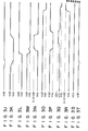
- the node N2 of the dummy cell capacitor is held at the voltage Vss (Fig. 3S). Assuming that the latch memory cell 20 stores bit data at logic level "0", initial potentials of the node lines Ai and Ai' are set at Vss and Vdd, respectively.
- the memory cell word line MW1 and the dummy cell word line DW2 are selected.
- the potential of the lines MW1 and DW2 rises from the voltage Vss to the voltage 1 Vdd, as shown in Figs. 3G and 3H, the MOSFETs Q16 and Q13 which are included in the cells MC1 and DC1 connected to the lines MWl and DW2 are rendered conductive.
- the capacitors C5 and C4 are electrically connected to the bit lines Bi and Bi' through the conductive MOSFETs Q16 and Q13, respectively. Therefore, electrical storage contents of the capacitors C5 and C4 are transferred onto the bit lines Bi and Bi'.
- the sense clock signal supplied to the clock line Kl for the sense-amplifier 10 gradually drops from a voltage difference between the voltages Vdd and Vth (indicated by "Vdd-Vth" in Fig. 31), to the ground potential Vss, as shown in Fig. 31.
- the sense-amplifier 10 is activated.
- Figs. 3J and 3K show changes in the potential of bit lines Bi and Bi'.
- the potential of the bit line Bi which reads out the "1" data from the memory cell MC1, is held at Vdd. At this time, the potential of the bit line Bi falls slightly and temporarily due to coupling and racing, with respect to the bit line Bi' as shown in Fig. 3J. However, this change in level is soon recovered, and the potential of the bit line Bi is constantly maintained at the voltage Vdd. This is because the clock signal supplied to the clock line K2, which is connected to the pull-up circuit 12, rises from the voltage Vss to the voltage Vdd, as shown in Fig. 3C, to start the pull-up operation of the circuit 12. Upon start of the active pull-up operation of the circuit 12, the FET Q5 is rendered conductive, thereby supplying the voltage Vdd to the bit line Bi through the FET Q5.
- the transfer gate FETs Q20 and Q21 are rendered conductive, and the first transfer gate 20-i is set in an "open" state.
- the bit lines Bi and Bi' are electrically connected to the node lines Ai and Ai', respectively.
- the readout data potentials appearing on the bit lines Bi and Bi' are transferred to the node lines Ai and Ai'.
- the potential of the lines A i and Ai' is changed, as shown in Figs. 3L and 3M. That is, the potential of the node line Ai, which is connected to the bit line Bi (i.e., the memory cell MC1), is changed from the ground potential Vss to the power supply voltage Vdd, as shown in Fig. 3L.
- the potential of the line Ai', which is connected to the bit line Bi' i.e., the dummy cell DC2
- the potentials of these lines, after the drop in potential, are statically held by the static flip-flop circuit.
- the other latch memory cells i.e., the static memory cells 20-1, 20-2,... shown in Fig. 1 are operated in the same manner as described above. Therefore, the potentials of all the memory cells connected to the designated memory cell word line (in this case, the line MW1) and those of the dummy cells connected to the dummy cell word line (in this case, the line DW2) are transferred to and held in the node line pairs A and A' of the corresponding latch memory cells. In other words, the storage contents of all the memory cells connected to a designated memory cell word line are statically stored in the corresponding latch memory cells 20-1, 20-2,..., 20-i,....
- Figs. 4A to 4T are waveform charts of electrical signals generated from the main parts of the dRAM of the embodiment when data held in the specific latch memory cell is to be written in the corresponding memory cell in the dRAM.
- Figs. 4A to 4T correspond to Figs. 3A to 3T.
- Figs. 4A and 4B show waveforms of the RAS and CAS signals.
- Figs. 4C to 4F show waveforms of the clock signals supplied to the clock lines K2 to K5. Figs.
- FIG. 41 shows a waveform of the clock signal supplied to the clock line Kl which is connected to the sense-amplifier 10.
- Figs. 4J and 4K show changes in potential of the ith bit line pair Bi and Bi'.
- Figs. 4L and 4M show changes in potential of the node line pair Ai and Ai' of the latch memory cell connected to the lines Bi and Bi'.
- Fig. 4N shows the waveform of the column select signal CSLi.
- Figs. 40 and 4P show changes in potential of the input/output line pair 50 and 50' .
- Fig. 4Q shows an output data potential.
- Fig. 41 shows a waveform of the clock signal supplied to the clock line Kl which is connected to the sense-amplifier 10.
- Figs. 4J and 4K show changes in potential of the ith bit line pair Bi and Bi'.
- Figs. 4L and 4M show changes in potential of the node line pair Ai and Ai' of the latch memory cell connected to the
- FIG. 4R shows the waveform of a column select signal CSLj (not shown in Fig. 2) supplied to the jth bit line pair.
- Figs. 4S and 4T show changes in potential of the capacitor nodes N2 and N1 of the dummy cell DC2 and the memory cell MC1 which are connected to the ith bit line pair.
- the pre-charge clock signal K3 falls from the voltage 3 2 Vdd to the voltage Vss (see Fig. 4D), thereby electrically floating the bit lines.
- the FETs Q14 and Q13 are rendered nonconductive. Therefore, the nodes N2 and N3 of the capacitors are insulated from the ground potential.
- the potential of the transfer gate drive clock signal K5 is changed from the voltage Vss to the voltage 1 V dd, as shown in Fig. 4F.
- the first transfer gate 30-i is set in the "open" state, and the latch memory cell 20-i is electrically connected to the bit lines Bi and Bi'.
- the latch memory cell 20 can statically store the data of the previously selected memory cell MC1 continuously even during the pre-charge period of the bit lines.
- the FETs Q20 and Q21 included in the first transfer gate section 30 are rendered conductive in response to the transfer gate drive clock signal K5
- the potentials of the node lines Ai and Ai' of the latch memory cell are transferred to the corresponding ith bit line pair Bi and Bi' through the transfer gate 20-i.
- the potential level of the bit line Bi falls from the voltage Vdd to the voltage Vss, as shown in Fig. 4J, and at the same time, the potential level of the bit line Bi' is continuously held at the power supply voltage Vdd, as shown in Fig. 4K.
- the dRAM with the auxiliary static cells of the present invention storage data of all the memory cells connected to a selected memory word line are supplied to the corresponding latch memory cells (20), and are statically held thereby. Such static data storage in the latch memory cells is continuously performed until the next word line is designated. Therefore, during the pre-charge period of the bit lines, performed in the above operation, if storage data in another memory cell must be read out from the memory cells connected to the selected word line, the latch memory cell corresponding to the certain memory cell can be designated so as to read out the data therefrom. If necessary, accessing of storage data of the latch memory cell can be repeated even in the pre-charge period until the next word line is designated. As for the memory cells connected to the selected word line, data accessing therebetween is not limited to the pre-charging operation, and can be repeated a desired number of times. Therefore, data access speed of the dRAM can be greatly improved.
- the folded bit line configuration has been exemplified.
- the present invention can be applied to a dRAM of an open end bit line configuration.
- the present invention can also be applied to a static RAM.
Landscapes
- Engineering & Computer Science (AREA)
- Computer Hardware Design (AREA)
- Microelectronics & Electronic Packaging (AREA)
- Databases & Information Systems (AREA)
- Dram (AREA)
Priority Applications (1)
| Application Number | Priority Date | Filing Date | Title |
|---|---|---|---|
| EP94118563A EP0640977B1 (de) | 1984-12-13 | 1985-12-13 | Dynamischer Halbleiterspeicher mit einer statischen Datenspeicherzelle |
Applications Claiming Priority (2)
| Application Number | Priority Date | Filing Date | Title |
|---|---|---|---|
| JP59263304A JPH0793009B2 (ja) | 1984-12-13 | 1984-12-13 | 半導体記憶装置 |
| JP263304/84 | 1984-12-13 |
Related Child Applications (2)
| Application Number | Title | Priority Date | Filing Date |
|---|---|---|---|
| EP94118563A Division EP0640977B1 (de) | 1984-12-13 | 1985-12-13 | Dynamischer Halbleiterspeicher mit einer statischen Datenspeicherzelle |
| EP94118563.9 Division-Into | 1994-11-25 |
Publications (3)
| Publication Number | Publication Date |
|---|---|
| EP0185529A2 true EP0185529A2 (de) | 1986-06-25 |
| EP0185529A3 EP0185529A3 (en) | 1988-08-17 |
| EP0185529B1 EP0185529B1 (de) | 1995-07-19 |
Family
ID=17387614
Family Applications (2)
| Application Number | Title | Priority Date | Filing Date |
|---|---|---|---|
| EP85309118A Expired - Lifetime EP0185529B1 (de) | 1984-12-13 | 1985-12-13 | Dynamischer Halbleiterspeicher mit einer statischen Datenspeicherzelle |
| EP94118563A Expired - Lifetime EP0640977B1 (de) | 1984-12-13 | 1985-12-13 | Dynamischer Halbleiterspeicher mit einer statischen Datenspeicherzelle |
Family Applications After (1)
| Application Number | Title | Priority Date | Filing Date |
|---|---|---|---|
| EP94118563A Expired - Lifetime EP0640977B1 (de) | 1984-12-13 | 1985-12-13 | Dynamischer Halbleiterspeicher mit einer statischen Datenspeicherzelle |
Country Status (5)
| Country | Link |
|---|---|
| US (1) | US4758987A (de) |
| EP (2) | EP0185529B1 (de) |
| JP (1) | JPH0793009B2 (de) |
| KR (1) | KR910004188B1 (de) |
| DE (2) | DE3588042T2 (de) |
Cited By (4)
| Publication number | Priority date | Publication date | Assignee | Title |
|---|---|---|---|---|
| EP0498107A3 (en) * | 1991-02-07 | 1993-01-13 | Mitsubishi Denki Kabushiki Kaisha | A semiconductor memory device with an internal voltage generating circuit |
| EP0540115A3 (en) * | 1991-10-31 | 1993-12-15 | Ibm | Early row address strobe (ras) precharge |
| EP0444707A3 (de) * | 1990-03-02 | 1994-03-30 | Nec Corp | |
| EP0548964A3 (en) * | 1991-12-23 | 1994-08-10 | Texas Instruments Inc | Combination dram and sram memory array |
Families Citing this family (41)
| Publication number | Priority date | Publication date | Assignee | Title |
|---|---|---|---|---|
| JPS6240698A (ja) * | 1985-08-16 | 1987-02-21 | Fujitsu Ltd | 半導体記憶装置 |
| JPS62146491A (ja) * | 1985-12-20 | 1987-06-30 | Sanyo Electric Co Ltd | 半導体メモリ |
| JPS62245593A (ja) * | 1986-04-17 | 1987-10-26 | Sanyo Electric Co Ltd | ダイナミツクメモリのデ−タ書き込み方法 |
| EP0293933B1 (de) * | 1987-06-04 | 1993-10-13 | Nec Corporation | Dynamische Speicherschaltung mit einem Abfühlschema |
| US4875196A (en) * | 1987-09-08 | 1989-10-17 | Sharp Microelectronic Technology, Inc. | Method of operating data buffer apparatus |
| US5173878A (en) * | 1987-11-25 | 1992-12-22 | Kabushiki Kaisha Toshiba | Semiconductor memory including address multiplexing circuitry for changing the order of supplying row and column addresses between read and write cycles |
| JP2713929B2 (ja) * | 1987-11-25 | 1998-02-16 | 株式会社東芝 | 半導体記憶装置 |
| US4943944A (en) * | 1987-11-25 | 1990-07-24 | Kabushiki Kaisha Toshiba | Semiconductor memory using dynamic ram cells |
| JPH01138680A (ja) * | 1987-11-25 | 1989-05-31 | Toshiba Corp | 半導体記憶装置 |
| JP2599747B2 (ja) * | 1988-03-10 | 1997-04-16 | 沖電気工業株式会社 | 半導体メモリの制御方法 |
| JP2633645B2 (ja) * | 1988-09-13 | 1997-07-23 | 株式会社東芝 | 半導体メモリ装置 |
| JPH07101554B2 (ja) * | 1988-11-29 | 1995-11-01 | 三菱電機株式会社 | 半導体記憶装置およびそのデータ転送方法 |
| JP2860403B2 (ja) * | 1988-12-22 | 1999-02-24 | リチャード・チャールズ・フォス | ダイナミック型半導体記憶装置 |
| JP2646032B2 (ja) * | 1989-10-14 | 1997-08-25 | 三菱電機株式会社 | Lifo方式の半導体記憶装置およびその制御方法 |
| JP2662822B2 (ja) * | 1990-03-20 | 1997-10-15 | 三菱電機株式会社 | 半導体記憶装置 |
| JPH0834257B2 (ja) * | 1990-04-20 | 1996-03-29 | 株式会社東芝 | 半導体メモリセル |
| JPH0457282A (ja) * | 1990-06-22 | 1992-02-25 | Mitsubishi Electric Corp | 半導体メモリ装置 |
| JPH07122989B2 (ja) * | 1990-06-27 | 1995-12-25 | 株式会社東芝 | 半導体記憶装置 |
| JP2604276B2 (ja) * | 1990-11-20 | 1997-04-30 | 三菱電機株式会社 | 半導体記憶装置 |
| EP0811979B1 (de) | 1990-12-25 | 2004-02-11 | Mitsubishi Denki Kabushiki Kaisha | Halbleiterspeichervorrichtung |
| JP2660111B2 (ja) * | 1991-02-13 | 1997-10-08 | 株式会社東芝 | 半導体メモリセル |
| JP2564046B2 (ja) * | 1991-02-13 | 1996-12-18 | 株式会社東芝 | 半導体記憶装置 |
| DE69222793T2 (de) * | 1991-03-14 | 1998-03-12 | Toshiba Kawasaki Kk | Halbleiterspeicheranordnung |
| JP3181311B2 (ja) * | 1991-05-29 | 2001-07-03 | 株式会社東芝 | 半導体記憶装置 |
| JP3464803B2 (ja) * | 1991-11-27 | 2003-11-10 | 株式会社東芝 | 半導体メモリセル |
| US5291437A (en) * | 1992-06-25 | 1994-03-01 | Texas Instruments Incorporated | Shared dummy cell |
| US5617093A (en) * | 1994-09-30 | 1997-04-01 | Imp, Inc. | Switched capacitor analog circuits with low input capacitance |
| US5836007A (en) * | 1995-09-14 | 1998-11-10 | International Business Machines Corporation | Methods and systems for improving memory component size and access speed including splitting bit lines and alternate pre-charge/access cycles |
| US6167486A (en) * | 1996-11-18 | 2000-12-26 | Nec Electronics, Inc. | Parallel access virtual channel memory system with cacheable channels |
| US5936874A (en) | 1997-06-19 | 1999-08-10 | Micron Technology, Inc. | High density semiconductor memory and method of making |
| US5982700A (en) * | 1998-05-21 | 1999-11-09 | Integrated Device Technology, Inc. | Buffer memory arrays having nonlinear columns for providing parallel data access capability and methods of operating same |
| US5978307A (en) * | 1998-05-21 | 1999-11-02 | Integrated Device Technology, Inc. | Integrated circuit memory devices having partitioned multi-port memory arrays therein for increasing data bandwidth and methods of operating same |
| US6216205B1 (en) | 1998-05-21 | 2001-04-10 | Integrated Device Technology, Inc. | Methods of controlling memory buffers having tri-port cache arrays therein |
| US5999478A (en) * | 1998-05-21 | 1999-12-07 | Integrated Device Technology, Inc. | Highly integrated tri-port memory buffers having fast fall-through capability and methods of operating same |
| JP2000011640A (ja) * | 1998-06-23 | 2000-01-14 | Nec Corp | 半導体記憶装置 |
| US6072746A (en) | 1998-08-14 | 2000-06-06 | International Business Machines Corporation | Self-timed address decoder for register file and compare circuit of a multi-port CAM |
| JP2000293984A (ja) | 1999-04-01 | 2000-10-20 | Toshiba Microelectronics Corp | 半導体記憶装置 |
| US6708254B2 (en) | 1999-11-10 | 2004-03-16 | Nec Electronics America, Inc. | Parallel access virtual channel memory system |
| KR100368133B1 (ko) | 2000-03-28 | 2003-01-15 | 한국과학기술원 | 메모리 셀 정보 저장 방법 |
| US6546461B1 (en) | 2000-11-22 | 2003-04-08 | Integrated Device Technology, Inc. | Multi-port cache memory devices and FIFO memory devices having multi-port cache memory devices therein |
| US7042792B2 (en) * | 2004-01-14 | 2006-05-09 | Integrated Device Technology, Inc. | Multi-port memory cells for use in FIFO applications that support data transfers between cache and supplemental memory arrays |
Family Cites Families (16)
| Publication number | Priority date | Publication date | Assignee | Title |
|---|---|---|---|---|
| US3646525A (en) * | 1970-01-12 | 1972-02-29 | Ibm | Data regeneration scheme without using memory sense amplifiers |
| JPS5032090B2 (de) * | 1972-06-20 | 1975-10-17 | ||
| US4004284A (en) * | 1975-03-05 | 1977-01-18 | Teletype Corporation | Binary voltage-differential sensing circuits, and sense/refresh amplifier circuits for random-access memories |
| JPS51113545A (en) * | 1975-03-31 | 1976-10-06 | Hitachi Ltd | Memory |
| US4508980A (en) * | 1976-11-11 | 1985-04-02 | Signetics Corporation | Sense and refresh amplifier circuit |
| US4106109A (en) * | 1977-02-01 | 1978-08-08 | Ncr Corporation | Random access memory system providing high-speed digital data output |
| US4354255A (en) * | 1980-04-29 | 1982-10-12 | Rca Corporation | Random access memory with volatile and non-volatile storage |
| US4351034A (en) * | 1980-10-10 | 1982-09-21 | Inmos Corporation | Folded bit line-shared sense amplifiers |
| US4363110A (en) * | 1980-12-22 | 1982-12-07 | International Business Machines Corp. | Non-volatile dynamic RAM cell |
| JPS57167186A (en) * | 1981-04-08 | 1982-10-14 | Nec Corp | Memory circuit |
| JPS5940397A (ja) * | 1982-08-31 | 1984-03-06 | Toshiba Corp | デ−タ読み出し回路 |
| JPS5960794A (ja) * | 1982-09-29 | 1984-04-06 | Fujitsu Ltd | ダイナミツク型半導体記憶装置 |
| JPS59119591A (ja) * | 1982-12-27 | 1984-07-10 | Toshiba Corp | 半導体メモリ装置 |
| JPH069114B2 (ja) * | 1983-06-24 | 1994-02-02 | 株式会社東芝 | 半導体メモリ |
| JPS60209996A (ja) * | 1984-03-31 | 1985-10-22 | Toshiba Corp | 半導体記憶装置 |
| JPS6190396A (ja) * | 1984-10-09 | 1986-05-08 | Nec Corp | ダイナミツクmosメモリ回路 |
-
1984
- 1984-12-13 JP JP59263304A patent/JPH0793009B2/ja not_active Expired - Lifetime
-
1985
- 1985-12-06 KR KR1019850009184A patent/KR910004188B1/ko not_active Expired
- 1985-12-09 US US06/806,498 patent/US4758987A/en not_active Expired - Lifetime
- 1985-12-13 DE DE3588042T patent/DE3588042T2/de not_active Expired - Fee Related
- 1985-12-13 DE DE3588247T patent/DE3588247T2/de not_active Expired - Lifetime
- 1985-12-13 EP EP85309118A patent/EP0185529B1/de not_active Expired - Lifetime
- 1985-12-13 EP EP94118563A patent/EP0640977B1/de not_active Expired - Lifetime
Cited By (5)
| Publication number | Priority date | Publication date | Assignee | Title |
|---|---|---|---|---|
| EP0444707A3 (de) * | 1990-03-02 | 1994-03-30 | Nec Corp | |
| EP0498107A3 (en) * | 1991-02-07 | 1993-01-13 | Mitsubishi Denki Kabushiki Kaisha | A semiconductor memory device with an internal voltage generating circuit |
| US6333873B1 (en) | 1991-02-07 | 2001-12-25 | Mitsubishi Denki Kabushiki Kaisha | Semiconductor memory device with an internal voltage generating circuit |
| EP0540115A3 (en) * | 1991-10-31 | 1993-12-15 | Ibm | Early row address strobe (ras) precharge |
| EP0548964A3 (en) * | 1991-12-23 | 1994-08-10 | Texas Instruments Inc | Combination dram and sram memory array |
Also Published As
| Publication number | Publication date |
|---|---|
| KR860005370A (ko) | 1986-07-21 |
| EP0640977A1 (de) | 1995-03-01 |
| JPS61142592A (ja) | 1986-06-30 |
| DE3588247T2 (de) | 2004-04-22 |
| EP0640977B1 (de) | 2003-07-09 |
| JPH0793009B2 (ja) | 1995-10-09 |
| DE3588042D1 (de) | 1995-08-24 |
| EP0185529B1 (de) | 1995-07-19 |
| EP0185529A3 (en) | 1988-08-17 |
| DE3588247D1 (de) | 2003-08-14 |
| DE3588042T2 (de) | 1995-12-21 |
| US4758987A (en) | 1988-07-19 |
| KR910004188B1 (ko) | 1991-06-24 |
Similar Documents
| Publication | Publication Date | Title |
|---|---|---|
| US4758987A (en) | Dynamic semiconductor memory with static data storing cell unit | |
| US4943944A (en) | Semiconductor memory using dynamic ram cells | |
| US4567579A (en) | Dynamic memory with high speed nibble mode | |
| EP0069764B1 (de) | Schreib-lese-speichersystem mit regelmässigen hochgeschwindigkeitsdatenwegen | |
| US5555212A (en) | Method and apparatus for redundancy word line replacement in a semiconductor memory device | |
| US5479370A (en) | Semiconductor memory with bypass circuit | |
| US8441878B2 (en) | Embedded memory databus architecture | |
| US4817057A (en) | Semiconductor memory device having improved precharge scheme | |
| EP0166974A2 (de) | Dynamischer Direktzugriffspeicher | |
| US5933363A (en) | Associative memory having comparator for detecting data match signal | |
| EP0030245A1 (de) | Halbleiter-speichervorrichtung | |
| US5892724A (en) | NAND-type dynamic RAM having temporary storage register and sense amplifier coupled to multi-open bit lines | |
| US4241425A (en) | Organization for dynamic random access memory | |
| EP0499256B1 (de) | Halbleiterspeichereinrichtung | |
| Eaton et al. | A 100ns 64K dynamic RAM using redundancy techniques | |
| JPS61160898A (ja) | 半導体記憶装置 | |
| US6205069B1 (en) | Semiconductor memory device with fast input/output line precharge scheme and method of precharging input/output lines thereof | |
| US5317540A (en) | Semiconductor memory device | |
| US5359566A (en) | Dynamic random access memory | |
| EP0676767B1 (de) | Kopierverfahren für eine DRAM-Seite | |
| JP2823466B2 (ja) | 半導体記憶装置 | |
| US5654933A (en) | Equilibrated sam read transfer circuit | |
| EP0166642A2 (de) | Blockunterteiltes Halbleiterspeichergerät mit unterteilten Bitzeilen | |
| US5337287A (en) | Dual port semiconductor memory device | |
| JPS6142794A (ja) | 半導体記憶装置のセンスアンプ系 |
Legal Events
| Date | Code | Title | Description |
|---|---|---|---|
| PUAI | Public reference made under article 153(3) epc to a published international application that has entered the european phase |
Free format text: ORIGINAL CODE: 0009012 |
|
| AK | Designated contracting states |
Kind code of ref document: A2 Designated state(s): DE FR GB IT |
|
| 17P | Request for examination filed |
Effective date: 19861002 |
|
| PUAL | Search report despatched |
Free format text: ORIGINAL CODE: 0009013 |
|
| AK | Designated contracting states |
Kind code of ref document: A3 Designated state(s): DE FR GB IT |
|
| 17Q | First examination report despatched |
Effective date: 19900129 |
|
| RBV | Designated contracting states (corrected) |
Designated state(s): DE FR GB |
|
| GRAA | (expected) grant |
Free format text: ORIGINAL CODE: 0009210 |
|
| AK | Designated contracting states |
Kind code of ref document: B1 Designated state(s): DE FR GB |
|
| XX | Miscellaneous (additional remarks) |
Free format text: TEILANMELDUNG 94118563.9 EINGEREICHT AM 13/12/85. |
|
| REF | Corresponds to: |
Ref document number: 3588042 Country of ref document: DE Date of ref document: 19950824 |
|
| ET | Fr: translation filed | ||
| PLBE | No opposition filed within time limit |
Free format text: ORIGINAL CODE: 0009261 |
|
| STAA | Information on the status of an ep patent application or granted ep patent |
Free format text: STATUS: NO OPPOSITION FILED WITHIN TIME LIMIT |
|
| 26N | No opposition filed | ||
| PGFP | Annual fee paid to national office [announced via postgrant information from national office to epo] |
Ref country code: FR Payment date: 19971209 Year of fee payment: 13 |
|
| PGFP | Annual fee paid to national office [announced via postgrant information from national office to epo] |
Ref country code: DE Payment date: 19971222 Year of fee payment: 13 |
|
| REG | Reference to a national code |
Ref country code: GB Ref legal event code: 746 Effective date: 19980929 |
|
| PG25 | Lapsed in a contracting state [announced via postgrant information from national office to epo] |
Ref country code: FR Free format text: LAPSE BECAUSE OF NON-PAYMENT OF DUE FEES Effective date: 19990831 |
|
| REG | Reference to a national code |
Ref country code: FR Ref legal event code: ST |
|
| PG25 | Lapsed in a contracting state [announced via postgrant information from national office to epo] |
Ref country code: DE Free format text: LAPSE BECAUSE OF NON-PAYMENT OF DUE FEES Effective date: 19991001 |
|
| REG | Reference to a national code |
Ref country code: GB Ref legal event code: IF02 |
|
| PGFP | Annual fee paid to national office [announced via postgrant information from national office to epo] |
Ref country code: GB Payment date: 20041208 Year of fee payment: 20 |
|
| PG25 | Lapsed in a contracting state [announced via postgrant information from national office to epo] |
Ref country code: GB Free format text: LAPSE BECAUSE OF EXPIRATION OF PROTECTION Effective date: 20051212 |
|
| REG | Reference to a national code |
Ref country code: GB Ref legal event code: PE20 |