EP0185529B1 - Dynamischer Halbleiterspeicher mit einer statischen Datenspeicherzelle - Google Patents
Dynamischer Halbleiterspeicher mit einer statischen Datenspeicherzelle Download PDFInfo
- Publication number
- EP0185529B1 EP0185529B1 EP85309118A EP85309118A EP0185529B1 EP 0185529 B1 EP0185529 B1 EP 0185529B1 EP 85309118 A EP85309118 A EP 85309118A EP 85309118 A EP85309118 A EP 85309118A EP 0185529 B1 EP0185529 B1 EP 0185529B1
- Authority
- EP
- European Patent Office
- Prior art keywords
- memory cell
- lines
- data
- auxiliary memory
- bit lines
- Prior art date
- Legal status (The legal status is an assumption and is not a legal conclusion. Google has not performed a legal analysis and makes no representation as to the accuracy of the status listed.)
- Expired - Lifetime
Links
- 230000003068 static effect Effects 0.000 title claims description 19
- 239000004065 semiconductor Substances 0.000 title claims description 7
- 238000012546 transfer Methods 0.000 claims description 33
- 239000003990 capacitor Substances 0.000 claims description 25
- 230000004044 response Effects 0.000 claims description 8
- 230000008859 change Effects 0.000 claims description 6
- 238000000034 method Methods 0.000 claims description 5
- 239000000758 substrate Substances 0.000 claims description 4
- 238000013500 data storage Methods 0.000 description 2
- 238000010586 diagram Methods 0.000 description 2
- 230000006872 improvement Effects 0.000 description 2
- 230000015556 catabolic process Effects 0.000 description 1
- 230000008878 coupling Effects 0.000 description 1
- 238000010168 coupling process Methods 0.000 description 1
- 238000005859 coupling reaction Methods 0.000 description 1
- 238000006731 degradation reaction Methods 0.000 description 1
- 238000011161 development Methods 0.000 description 1
- 230000018109 developmental process Effects 0.000 description 1
- 230000005669 field effect Effects 0.000 description 1
- 229910044991 metal oxide Inorganic materials 0.000 description 1
- 150000004706 metal oxides Chemical class 0.000 description 1
- 238000012986 modification Methods 0.000 description 1
- 230000004048 modification Effects 0.000 description 1
- 238000000059 patterning Methods 0.000 description 1
- 238000012545 processing Methods 0.000 description 1
Images



Classifications
-
- G—PHYSICS
- G11—INFORMATION STORAGE
- G11C—STATIC STORES
- G11C11/00—Digital stores characterised by the use of particular electric or magnetic storage elements; Storage elements therefor
- G11C11/21—Digital stores characterised by the use of particular electric or magnetic storage elements; Storage elements therefor using electric elements
- G11C11/34—Digital stores characterised by the use of particular electric or magnetic storage elements; Storage elements therefor using electric elements using semiconductor devices
- G11C11/40—Digital stores characterised by the use of particular electric or magnetic storage elements; Storage elements therefor using electric elements using semiconductor devices using transistors
-
- G—PHYSICS
- G11—INFORMATION STORAGE
- G11C—STATIC STORES
- G11C7/00—Arrangements for writing information into, or reading information out from, a digital store
- G11C7/10—Input/output [I/O] data interface arrangements, e.g. I/O data control circuits, I/O data buffers
- G11C7/1051—Data output circuits, e.g. read-out amplifiers, data output buffers, data output registers, data output level conversion circuits
- G11C7/106—Data output latches
-
- G—PHYSICS
- G11—INFORMATION STORAGE
- G11C—STATIC STORES
- G11C11/00—Digital stores characterised by the use of particular electric or magnetic storage elements; Storage elements therefor
- G11C11/005—Digital stores characterised by the use of particular electric or magnetic storage elements; Storage elements therefor comprising combined but independently operative RAM-ROM, RAM-PROM, RAM-EPROM cells
-
- G—PHYSICS
- G11—INFORMATION STORAGE
- G11C—STATIC STORES
- G11C11/00—Digital stores characterised by the use of particular electric or magnetic storage elements; Storage elements therefor
- G11C11/21—Digital stores characterised by the use of particular electric or magnetic storage elements; Storage elements therefor using electric elements
- G11C11/34—Digital stores characterised by the use of particular electric or magnetic storage elements; Storage elements therefor using electric elements using semiconductor devices
- G11C11/40—Digital stores characterised by the use of particular electric or magnetic storage elements; Storage elements therefor using electric elements using semiconductor devices using transistors
- G11C11/401—Digital stores characterised by the use of particular electric or magnetic storage elements; Storage elements therefor using electric elements using semiconductor devices using transistors forming cells needing refreshing or charge regeneration, i.e. dynamic cells
- G11C11/4063—Auxiliary circuits, e.g. for addressing, decoding, driving, writing, sensing or timing
- G11C11/407—Auxiliary circuits, e.g. for addressing, decoding, driving, writing, sensing or timing for memory cells of the field-effect type
- G11C11/409—Read-write [R-W] circuits
- G11C11/4096—Input/output [I/O] data management or control circuits, e.g. reading or writing circuits, I/O drivers or bit-line switches
-
- G—PHYSICS
- G11—INFORMATION STORAGE
- G11C—STATIC STORES
- G11C7/00—Arrangements for writing information into, or reading information out from, a digital store
- G11C7/10—Input/output [I/O] data interface arrangements, e.g. I/O data control circuits, I/O data buffers
- G11C7/1051—Data output circuits, e.g. read-out amplifiers, data output buffers, data output registers, data output level conversion circuits
-
- G—PHYSICS
- G11—INFORMATION STORAGE
- G11C—STATIC STORES
- G11C7/00—Arrangements for writing information into, or reading information out from, a digital store
- G11C7/10—Input/output [I/O] data interface arrangements, e.g. I/O data control circuits, I/O data buffers
- G11C7/1078—Data input circuits, e.g. write amplifiers, data input buffers, data input registers, data input level conversion circuits
-
- G—PHYSICS
- G11—INFORMATION STORAGE
- G11C—STATIC STORES
- G11C7/00—Arrangements for writing information into, or reading information out from, a digital store
- G11C7/10—Input/output [I/O] data interface arrangements, e.g. I/O data control circuits, I/O data buffers
- G11C7/1078—Data input circuits, e.g. write amplifiers, data input buffers, data input registers, data input level conversion circuits
- G11C7/1087—Data input latches
Definitions
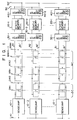
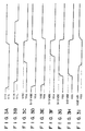
- the sense clock signal supplied to the clock line K1 for the sense-amplifier 10 gradually drops from a voltage difference between the voltages Vdd and Vth (indicated by "Vdd-Vth" in Fig. 3I), to the ground potential Vss, as shown in Fig. 31.
- the sense-amplifier 10 is activated.
- Figs. 3J and 3K show changes in the potential of bit lines Bi and Bi′.
- the folded bit line configuration has been exemplified.
- the present invention can be applied to a dRAM of an open end bit line configuration.
- the present invention can also be applied to a static RAM.
Landscapes
- Engineering & Computer Science (AREA)
- Computer Hardware Design (AREA)
- Microelectronics & Electronic Packaging (AREA)
- Databases & Information Systems (AREA)
- Dram (AREA)
Claims (6)
- Dynamische Halbleiterspeichervorrichtung mit:
zwei oder mehr parallelen Bitleitungen (B, B′), die auf einem Substrat gebildet sind,
zwei oder mehr parallelen Wortleitungen (MW1, MW2, ..., MW(n-1), MW), die im wesentlichen senkrecht zu den Bitleitungen vorgesehen sind,
einer oder mehr dynamischen Speicherzellen (MC1, MC2, ..., MC(n-1), MCn), die an Schnittstellen der Bitleitungen und der Wortleitungen vorgesehen sind,
einem Paar von Dateneingangs/ausgangsleitungen (50, 50′),
einer mit den Bitleitungen verbundenen Leseverstärkereinrichtung, um in einem Datenzugriffmodus der Speichervorrichtung eine in einer gewählten dynamischen Speicherzelle, die mit einer gewissen Wortleitung verbunden ist, gespeicherte Datenspannung abzutasten und zu verstärken,
einer mit den Bitleitungen verbundenen Hilfsspeicherzelleneinrichtung (20) zum statischen Speichern der darauf gespeisten Datenspannung,
einer mit den Bitleitungen, der Hilfsspeicherzelleneinrichtung und den Dateneingangs/ausgangsleitungen verbundenen Transfergattereinrichtung (30, 40), um Datenspannungen, die in dynamischen Speicherzellen gespeichert sind, die mit der gewissen Wortleitung verbunden sind, zu der Hilfsspeicherzelleneinrichtung zu übertragen und um selbst während einer Vorladeperiode elektrisch die Hilfsspeicherzelleneinrichtung mit den Dateneingangs/ausgangsleitungen zu verbinden, wodurch irgendeine der Datenspannungen zu den Dateneingangs/ausgangsleitungen selbst während der Vorladeperiode ausgelesen werden kann, wobei die Transfergattereinrichtung aufweist:
eine erste Transfergatterschaltungseinrichtung (30), die zwischen den Bitleitungen (B, B′) und der Hilfsspeicherzelleneinrichtung (20) vorgesehen ist, mit Transfertransistoren, die für jede Bitleitung einen Transfertransistor (Q20, Q21) umfassen, der allein zu der elektrischen Verbindung von der einen Bitleitung (B, B′) mit einer entsprechenden Hilfsspeicherzelleneinrichtung in dem Datenzugriffmodus und in dem Datenschreibmodus zugeordnet ist, um die Hilfsspeicherzelleneinrichtung von den Bitleitungen abhängig von einer Änderung in dem Potentialpegel eines Triggerimpulssignales zu trennen, das extern dort eingespeist ist, wodurch die Datenspannungen, die gerade in den dynamischen Speicherzellen gespeichert sind, die einer gewählten Wortleitung zugeordnet sind, im wesentlichen gleichzeitig zu der Hilfsspeicherzelleneinrichtung übertragen werden, wobei die Transfertransistoren durch eine gemeinsame Gattersteuerleitung (K5) gesteuert sind, und
eine zweite Transfergatterschaltungseinrichtung (40), die zwischen der Hilfsspeicherzelleneinrichtung und den Dateneingangs/ausgangsleitungen vorgesehen ist, um elektrisch die Hilfsspeicherzelleneinrichtung mit den Dateneingangs/ausgangsleitungen in dem Vorlademodus zu verbinden, so daß irgendeine der in der Hilfsspeicherzelleneinrichtung gespeicherten Datenspannungen auf die Dateneingangs/ausgangsleitungen ausgelesen werden kann. - Vorrichtung nach Anspruch 1, dadurch gekennzeichnet, daß die Hilfsspeicherzelleneinrichtung aufweist:
eine Array von statischen Speicherzellen (20), die jeweils mit den Bitleitungen (B, B′) verbunden sind, wobei jede der statischen Speicherzellen eine statische Flipflopschaltung umfaßt. - Vorrichtung nach Anspruch 2, dadurch gekennzeichnet, daß jede der Bitleitungen ein erstes Ende hat, mit welchem eine entsprechende Leseverstärkereinrichtung (10) verbunden ist, und daß jede Bitleitung ein zweites Ende aufweist, mit welchem eine entsprechende statische Speicherzelle (20) über die erste Transfergatterschaltungseinrichtung (30) verbunden ist.
- Vorrichtung nach Anspruch 3, dadurch gekennzeichnet, daß die ersten und zweiten Transfergatterschaltungseinrichtungen (30, 40) Schalttransistoren umfassen.
- Vorrichtung nach Anspruch 4, dadurch gekennzeichnet, daß jede der dynamischen Speicherzellen (MC) einen Schalttransistor (Q16, Q17, Q18, Q19) und einen Kondensator (C5, C5, C7, C8) umfaßt.
- Verfahren zum Betreiben einer dynamischen Halbleiterspeichervorrichtung nach einem der vorangehenden Ansprüche, umfassend ein Trennen der Hilfsspeicherzelleneinrichtung von den Bitleitungen abhängig von einer Änderung in dem Potentialpegel eines dort extern eingespeisten Strobe- oder Abtastsignales, um im wesentlichen gleichzeitig zu der Hilfsspeicherzelleneinrichtung die Datenspannungen zu übertragen, die in den dynamischen Speicherzellen gespeichert sind, die einer gewählten Wortleitung zugeordnet sind, und Betreiben der zweiten Transfergatterschaltungseinrichtung, um elektrisch die Hilfsspeicherzelleneinrichtung mit den Dateneingangs/ausgangsleitungen in dem Vorlademodus der Vorrichtung zu verbinden, damit eine der in der Hilfsspeicherzelleneinrichtung gespeicherten Datenspannungen auf die Dateneingangs/ausgangsleitungen ausgelesen werden.
Priority Applications (1)
| Application Number | Priority Date | Filing Date | Title |
|---|---|---|---|
| EP94118563A EP0640977B1 (de) | 1984-12-13 | 1985-12-13 | Dynamischer Halbleiterspeicher mit einer statischen Datenspeicherzelle |
Applications Claiming Priority (2)
| Application Number | Priority Date | Filing Date | Title |
|---|---|---|---|
| JP59263304A JPH0793009B2 (ja) | 1984-12-13 | 1984-12-13 | 半導体記憶装置 |
| JP263304/84 | 1984-12-13 |
Related Child Applications (2)
| Application Number | Title | Priority Date | Filing Date |
|---|---|---|---|
| EP94118563A Division EP0640977B1 (de) | 1984-12-13 | 1985-12-13 | Dynamischer Halbleiterspeicher mit einer statischen Datenspeicherzelle |
| EP94118563.9 Division-Into | 1994-11-25 |
Publications (3)
| Publication Number | Publication Date |
|---|---|
| EP0185529A2 EP0185529A2 (de) | 1986-06-25 |
| EP0185529A3 EP0185529A3 (en) | 1988-08-17 |
| EP0185529B1 true EP0185529B1 (de) | 1995-07-19 |
Family
ID=17387614
Family Applications (2)
| Application Number | Title | Priority Date | Filing Date |
|---|---|---|---|
| EP85309118A Expired - Lifetime EP0185529B1 (de) | 1984-12-13 | 1985-12-13 | Dynamischer Halbleiterspeicher mit einer statischen Datenspeicherzelle |
| EP94118563A Expired - Lifetime EP0640977B1 (de) | 1984-12-13 | 1985-12-13 | Dynamischer Halbleiterspeicher mit einer statischen Datenspeicherzelle |
Family Applications After (1)
| Application Number | Title | Priority Date | Filing Date |
|---|---|---|---|
| EP94118563A Expired - Lifetime EP0640977B1 (de) | 1984-12-13 | 1985-12-13 | Dynamischer Halbleiterspeicher mit einer statischen Datenspeicherzelle |
Country Status (5)
| Country | Link |
|---|---|
| US (1) | US4758987A (de) |
| EP (2) | EP0185529B1 (de) |
| JP (1) | JPH0793009B2 (de) |
| KR (1) | KR910004188B1 (de) |
| DE (2) | DE3588042T2 (de) |
Families Citing this family (45)
| Publication number | Priority date | Publication date | Assignee | Title |
|---|---|---|---|---|
| JPS6240698A (ja) * | 1985-08-16 | 1987-02-21 | Fujitsu Ltd | 半導体記憶装置 |
| JPS62146491A (ja) * | 1985-12-20 | 1987-06-30 | Sanyo Electric Co Ltd | 半導体メモリ |
| JPS62245593A (ja) * | 1986-04-17 | 1987-10-26 | Sanyo Electric Co Ltd | ダイナミツクメモリのデ−タ書き込み方法 |
| EP0293933B1 (de) * | 1987-06-04 | 1993-10-13 | Nec Corporation | Dynamische Speicherschaltung mit einem Abfühlschema |
| US4875196A (en) * | 1987-09-08 | 1989-10-17 | Sharp Microelectronic Technology, Inc. | Method of operating data buffer apparatus |
| US5173878A (en) * | 1987-11-25 | 1992-12-22 | Kabushiki Kaisha Toshiba | Semiconductor memory including address multiplexing circuitry for changing the order of supplying row and column addresses between read and write cycles |
| JP2713929B2 (ja) * | 1987-11-25 | 1998-02-16 | 株式会社東芝 | 半導体記憶装置 |
| US4943944A (en) * | 1987-11-25 | 1990-07-24 | Kabushiki Kaisha Toshiba | Semiconductor memory using dynamic ram cells |
| JPH01138680A (ja) * | 1987-11-25 | 1989-05-31 | Toshiba Corp | 半導体記憶装置 |
| JP2599747B2 (ja) * | 1988-03-10 | 1997-04-16 | 沖電気工業株式会社 | 半導体メモリの制御方法 |
| JP2633645B2 (ja) * | 1988-09-13 | 1997-07-23 | 株式会社東芝 | 半導体メモリ装置 |
| JPH07101554B2 (ja) * | 1988-11-29 | 1995-11-01 | 三菱電機株式会社 | 半導体記憶装置およびそのデータ転送方法 |
| JP2860403B2 (ja) * | 1988-12-22 | 1999-02-24 | リチャード・チャールズ・フォス | ダイナミック型半導体記憶装置 |
| JP2646032B2 (ja) * | 1989-10-14 | 1997-08-25 | 三菱電機株式会社 | Lifo方式の半導体記憶装置およびその制御方法 |
| JPH03252988A (ja) * | 1990-03-02 | 1991-11-12 | Nec Corp | ダイナミック型半導体メモリ |
| JP2662822B2 (ja) * | 1990-03-20 | 1997-10-15 | 三菱電機株式会社 | 半導体記憶装置 |
| JPH0834257B2 (ja) * | 1990-04-20 | 1996-03-29 | 株式会社東芝 | 半導体メモリセル |
| JPH0457282A (ja) * | 1990-06-22 | 1992-02-25 | Mitsubishi Electric Corp | 半導体メモリ装置 |
| JPH07122989B2 (ja) * | 1990-06-27 | 1995-12-25 | 株式会社東芝 | 半導体記憶装置 |
| JP2604276B2 (ja) * | 1990-11-20 | 1997-04-30 | 三菱電機株式会社 | 半導体記憶装置 |
| EP0811979B1 (de) | 1990-12-25 | 2004-02-11 | Mitsubishi Denki Kabushiki Kaisha | Halbleiterspeichervorrichtung |
| JPH04255989A (ja) | 1991-02-07 | 1992-09-10 | Mitsubishi Electric Corp | 半導体記憶装置および内部電圧発生方法 |
| JP2660111B2 (ja) * | 1991-02-13 | 1997-10-08 | 株式会社東芝 | 半導体メモリセル |
| JP2564046B2 (ja) * | 1991-02-13 | 1996-12-18 | 株式会社東芝 | 半導体記憶装置 |
| DE69222793T2 (de) * | 1991-03-14 | 1998-03-12 | Toshiba Kawasaki Kk | Halbleiterspeicheranordnung |
| JP3181311B2 (ja) * | 1991-05-29 | 2001-07-03 | 株式会社東芝 | 半導体記憶装置 |
| US5297091A (en) * | 1991-10-31 | 1994-03-22 | International Business Machines Corporation | Early row address strobe (RAS) precharge |
| JP3464803B2 (ja) * | 1991-11-27 | 2003-11-10 | 株式会社東芝 | 半導体メモリセル |
| US5291444A (en) * | 1991-12-23 | 1994-03-01 | Texas Instruments Incorporated | Combination DRAM and SRAM memory array |
| US5291437A (en) * | 1992-06-25 | 1994-03-01 | Texas Instruments Incorporated | Shared dummy cell |
| US5617093A (en) * | 1994-09-30 | 1997-04-01 | Imp, Inc. | Switched capacitor analog circuits with low input capacitance |
| US5836007A (en) * | 1995-09-14 | 1998-11-10 | International Business Machines Corporation | Methods and systems for improving memory component size and access speed including splitting bit lines and alternate pre-charge/access cycles |
| US6167486A (en) * | 1996-11-18 | 2000-12-26 | Nec Electronics, Inc. | Parallel access virtual channel memory system with cacheable channels |
| US5936874A (en) | 1997-06-19 | 1999-08-10 | Micron Technology, Inc. | High density semiconductor memory and method of making |
| US5982700A (en) * | 1998-05-21 | 1999-11-09 | Integrated Device Technology, Inc. | Buffer memory arrays having nonlinear columns for providing parallel data access capability and methods of operating same |
| US5978307A (en) * | 1998-05-21 | 1999-11-02 | Integrated Device Technology, Inc. | Integrated circuit memory devices having partitioned multi-port memory arrays therein for increasing data bandwidth and methods of operating same |
| US6216205B1 (en) | 1998-05-21 | 2001-04-10 | Integrated Device Technology, Inc. | Methods of controlling memory buffers having tri-port cache arrays therein |
| US5999478A (en) * | 1998-05-21 | 1999-12-07 | Integrated Device Technology, Inc. | Highly integrated tri-port memory buffers having fast fall-through capability and methods of operating same |
| JP2000011640A (ja) * | 1998-06-23 | 2000-01-14 | Nec Corp | 半導体記憶装置 |
| US6072746A (en) | 1998-08-14 | 2000-06-06 | International Business Machines Corporation | Self-timed address decoder for register file and compare circuit of a multi-port CAM |
| JP2000293984A (ja) | 1999-04-01 | 2000-10-20 | Toshiba Microelectronics Corp | 半導体記憶装置 |
| US6708254B2 (en) | 1999-11-10 | 2004-03-16 | Nec Electronics America, Inc. | Parallel access virtual channel memory system |
| KR100368133B1 (ko) | 2000-03-28 | 2003-01-15 | 한국과학기술원 | 메모리 셀 정보 저장 방법 |
| US6546461B1 (en) | 2000-11-22 | 2003-04-08 | Integrated Device Technology, Inc. | Multi-port cache memory devices and FIFO memory devices having multi-port cache memory devices therein |
| US7042792B2 (en) * | 2004-01-14 | 2006-05-09 | Integrated Device Technology, Inc. | Multi-port memory cells for use in FIFO applications that support data transfers between cache and supplemental memory arrays |
Family Cites Families (16)
| Publication number | Priority date | Publication date | Assignee | Title |
|---|---|---|---|---|
| US3646525A (en) * | 1970-01-12 | 1972-02-29 | Ibm | Data regeneration scheme without using memory sense amplifiers |
| JPS5032090B2 (de) * | 1972-06-20 | 1975-10-17 | ||
| US4004284A (en) * | 1975-03-05 | 1977-01-18 | Teletype Corporation | Binary voltage-differential sensing circuits, and sense/refresh amplifier circuits for random-access memories |
| JPS51113545A (en) * | 1975-03-31 | 1976-10-06 | Hitachi Ltd | Memory |
| US4508980A (en) * | 1976-11-11 | 1985-04-02 | Signetics Corporation | Sense and refresh amplifier circuit |
| US4106109A (en) * | 1977-02-01 | 1978-08-08 | Ncr Corporation | Random access memory system providing high-speed digital data output |
| US4354255A (en) * | 1980-04-29 | 1982-10-12 | Rca Corporation | Random access memory with volatile and non-volatile storage |
| US4351034A (en) * | 1980-10-10 | 1982-09-21 | Inmos Corporation | Folded bit line-shared sense amplifiers |
| US4363110A (en) * | 1980-12-22 | 1982-12-07 | International Business Machines Corp. | Non-volatile dynamic RAM cell |
| JPS57167186A (en) * | 1981-04-08 | 1982-10-14 | Nec Corp | Memory circuit |
| JPS5940397A (ja) * | 1982-08-31 | 1984-03-06 | Toshiba Corp | デ−タ読み出し回路 |
| JPS5960794A (ja) * | 1982-09-29 | 1984-04-06 | Fujitsu Ltd | ダイナミツク型半導体記憶装置 |
| JPS59119591A (ja) * | 1982-12-27 | 1984-07-10 | Toshiba Corp | 半導体メモリ装置 |
| JPH069114B2 (ja) * | 1983-06-24 | 1994-02-02 | 株式会社東芝 | 半導体メモリ |
| JPS60209996A (ja) * | 1984-03-31 | 1985-10-22 | Toshiba Corp | 半導体記憶装置 |
| JPS6190396A (ja) * | 1984-10-09 | 1986-05-08 | Nec Corp | ダイナミツクmosメモリ回路 |
-
1984
- 1984-12-13 JP JP59263304A patent/JPH0793009B2/ja not_active Expired - Lifetime
-
1985
- 1985-12-06 KR KR1019850009184A patent/KR910004188B1/ko not_active Expired
- 1985-12-09 US US06/806,498 patent/US4758987A/en not_active Expired - Lifetime
- 1985-12-13 DE DE3588042T patent/DE3588042T2/de not_active Expired - Fee Related
- 1985-12-13 DE DE3588247T patent/DE3588247T2/de not_active Expired - Lifetime
- 1985-12-13 EP EP85309118A patent/EP0185529B1/de not_active Expired - Lifetime
- 1985-12-13 EP EP94118563A patent/EP0640977B1/de not_active Expired - Lifetime
Also Published As
| Publication number | Publication date |
|---|---|
| KR860005370A (ko) | 1986-07-21 |
| EP0185529A2 (de) | 1986-06-25 |
| EP0640977A1 (de) | 1995-03-01 |
| JPS61142592A (ja) | 1986-06-30 |
| DE3588247T2 (de) | 2004-04-22 |
| EP0640977B1 (de) | 2003-07-09 |
| JPH0793009B2 (ja) | 1995-10-09 |
| DE3588042D1 (de) | 1995-08-24 |
| EP0185529A3 (en) | 1988-08-17 |
| DE3588247D1 (de) | 2003-08-14 |
| DE3588042T2 (de) | 1995-12-21 |
| US4758987A (en) | 1988-07-19 |
| KR910004188B1 (ko) | 1991-06-24 |
Similar Documents
| Publication | Publication Date | Title |
|---|---|---|
| EP0185529B1 (de) | Dynamischer Halbleiterspeicher mit einer statischen Datenspeicherzelle | |
| US4567579A (en) | Dynamic memory with high speed nibble mode | |
| EP0129651B1 (de) | Dynamischer Halbleiterspeicher mit Leseverstärkern | |
| EP0135940B1 (de) | Doppeltor-Speicheranordnung | |
| EP0069764B1 (de) | Schreib-lese-speichersystem mit regelmässigen hochgeschwindigkeitsdatenwegen | |
| KR970005283B1 (ko) | 반도체 기억장치 | |
| US5754486A (en) | Self-test circuit for memory integrated circuits | |
| US4473895A (en) | Semiconductor memory device | |
| US4817057A (en) | Semiconductor memory device having improved precharge scheme | |
| JPH01137491A (ja) | 半導体記憶装置 | |
| US5742544A (en) | Wide databus architecture | |
| US5274596A (en) | Dynamic semiconductor memory device having simultaneous operation of adjacent blocks | |
| JPS6374199A (ja) | 半導体記憶装置 | |
| EP0499256B1 (de) | Halbleiterspeichereinrichtung | |
| JPS61160898A (ja) | 半導体記憶装置 | |
| US6205069B1 (en) | Semiconductor memory device with fast input/output line precharge scheme and method of precharging input/output lines thereof | |
| US5317540A (en) | Semiconductor memory device | |
| JP3481263B2 (ja) | シリアル記憶装置 | |
| US4054865A (en) | Sense latch circuit for a bisectional memory array | |
| HK106193A (en) | Method and circuit arrangement for the parallel write-in of data in a semiconductor memory | |
| US5359566A (en) | Dynamic random access memory | |
| US4198697A (en) | Multiple dummy cell layout for MOS random access memory | |
| KR0139305B1 (ko) | 반도체 기억장치 | |
| EP0166642A2 (de) | Blockunterteiltes Halbleiterspeichergerät mit unterteilten Bitzeilen | |
| US5341332A (en) | Semiconductor memory device capable of flash writing and method of flash writing |
Legal Events
| Date | Code | Title | Description |
|---|---|---|---|
| PUAI | Public reference made under article 153(3) epc to a published international application that has entered the european phase |
Free format text: ORIGINAL CODE: 0009012 |
|
| AK | Designated contracting states |
Kind code of ref document: A2 Designated state(s): DE FR GB IT |
|
| 17P | Request for examination filed |
Effective date: 19861002 |
|
| PUAL | Search report despatched |
Free format text: ORIGINAL CODE: 0009013 |
|
| AK | Designated contracting states |
Kind code of ref document: A3 Designated state(s): DE FR GB IT |
|
| 17Q | First examination report despatched |
Effective date: 19900129 |
|
| RBV | Designated contracting states (corrected) |
Designated state(s): DE FR GB |
|
| GRAA | (expected) grant |
Free format text: ORIGINAL CODE: 0009210 |
|
| AK | Designated contracting states |
Kind code of ref document: B1 Designated state(s): DE FR GB |
|
| XX | Miscellaneous (additional remarks) |
Free format text: TEILANMELDUNG 94118563.9 EINGEREICHT AM 13/12/85. |
|
| REF | Corresponds to: |
Ref document number: 3588042 Country of ref document: DE Date of ref document: 19950824 |
|
| ET | Fr: translation filed | ||
| PLBE | No opposition filed within time limit |
Free format text: ORIGINAL CODE: 0009261 |
|
| STAA | Information on the status of an ep patent application or granted ep patent |
Free format text: STATUS: NO OPPOSITION FILED WITHIN TIME LIMIT |
|
| 26N | No opposition filed | ||
| PGFP | Annual fee paid to national office [announced via postgrant information from national office to epo] |
Ref country code: FR Payment date: 19971209 Year of fee payment: 13 |
|
| PGFP | Annual fee paid to national office [announced via postgrant information from national office to epo] |
Ref country code: DE Payment date: 19971222 Year of fee payment: 13 |
|
| REG | Reference to a national code |
Ref country code: GB Ref legal event code: 746 Effective date: 19980929 |
|
| PG25 | Lapsed in a contracting state [announced via postgrant information from national office to epo] |
Ref country code: FR Free format text: LAPSE BECAUSE OF NON-PAYMENT OF DUE FEES Effective date: 19990831 |
|
| REG | Reference to a national code |
Ref country code: FR Ref legal event code: ST |
|
| PG25 | Lapsed in a contracting state [announced via postgrant information from national office to epo] |
Ref country code: DE Free format text: LAPSE BECAUSE OF NON-PAYMENT OF DUE FEES Effective date: 19991001 |
|
| REG | Reference to a national code |
Ref country code: GB Ref legal event code: IF02 |
|
| PGFP | Annual fee paid to national office [announced via postgrant information from national office to epo] |
Ref country code: GB Payment date: 20041208 Year of fee payment: 20 |
|
| PG25 | Lapsed in a contracting state [announced via postgrant information from national office to epo] |
Ref country code: GB Free format text: LAPSE BECAUSE OF EXPIRATION OF PROTECTION Effective date: 20051212 |
|
| REG | Reference to a national code |
Ref country code: GB Ref legal event code: PE20 |