EP0324506A2 - Procédé et appareil pour la génération de données de dessins dégradés - Google Patents
Procédé et appareil pour la génération de données de dessins dégradés Download PDFInfo
- Publication number
- EP0324506A2 EP0324506A2 EP89100596A EP89100596A EP0324506A2 EP 0324506 A2 EP0324506 A2 EP 0324506A2 EP 89100596 A EP89100596 A EP 89100596A EP 89100596 A EP89100596 A EP 89100596A EP 0324506 A2 EP0324506 A2 EP 0324506A2
- Authority
- EP
- European Patent Office
- Prior art keywords
- line
- areas
- width
- image
- inv
- Prior art date
- Legal status (The legal status is an assumption and is not a legal conclusion. Google has not performed a legal analysis and makes no representation as to the accuracy of the status listed.)
- Granted
Links
Images


Classifications
-
- H—ELECTRICITY
- H04—ELECTRIC COMMUNICATION TECHNIQUE
- H04N—PICTORIAL COMMUNICATION, e.g. TELEVISION
- H04N1/00—Scanning, transmission or reproduction of documents or the like, e.g. facsimile transmission; Details thereof
- H04N1/46—Colour picture communication systems
Definitions
- the present invention relates to a method of and an apparatus for generating tint pattern data used for producing tint patterns by which a color print is reproduced.
- tint patterns producing respective uniform colors are printed on a same printing paper to produce a color print on which respective tint patterns are printed in contact with each other without a blank line between them.
- a line drawing is manually prepared by a designer, which line drawing defines outlines of different pattern areas to which respective uniform colors are assigned.
- a block copy of the line drawing is made and a positive picture of the block copy is taken as an original to be set for a process scanner.
- the process scanner reads the original picture to produce image data expressing the line drawing.
- An operater determines the respective uniform colors for the different pattern areas in the drawing, through inputting color-assigning data into the process scanner.
- the process scanner generates tint pattern data expressing the colors in respective pattern areas of the line drawing and produces halftone positives or halftone negatives of the tint patterns on the basis of the tint pattern data.
- tint pattern data are so generated as to express the colors only at the inside of the outlines
- a printed matter to be produced on the basis of the tint pattern data inlcudes blank lines, that is, white lines on which no inks are printed in place of the outlines.
- the tint patterns may be expanded to cover the areas on which the outlines are positions.
- the tint pattern data are modified to expand the tint patterns by a constant width all around under the condition that the constant width is smaller than the largest width of the outlines, some blank lines appears at some areas on a printed matter where parts of the outlines of larger width than the constant width are positioned.
- the constant width is larger than the smallest width of the outlines, two different color inks of the neighboring pattern areas are overlapped on areas where parts of the outlines of smaller width than the constant width are positioned.
- the present invention is directed to a method of and an apparatus for generating tint pattern data used for producing tint patterns by which a color print is reproduced, the method comprising the steps of: (a) preparing a first image data expressing a first image including a line having finite width, a first area and a second area, where the first and second areas are separeted from each other across the line, (b) executing a thinning process on the first image data in order to reduce width of the line to form a thinned line having a uniform width, to thereby obtain a second image data expressing a second image including the thinned line, an enlarged first area and an enlarged second area, where the enlarged first and second areas are separated from each other across the thinned line, (c) generating third and fourth image data expressing shapes of the enlarged first and second areas, respectively, (d) executing an expansion process on the third and fourth image data in order to expand the enlarged first and second areas by a constant width to form first and second expanded areas, respectively
- the first through sixth image data are formed as binary data assigned to each pixel, and the thinning process and the expansion process are performed through first and second logical processing, respectively, where a pixel cluster consisting of a plurality of pixels is previously defined, respective binary data for the plurality of the pixels are subjected to the first and second logical processings, and binary data of a central portion of the pixel cluster is replaced by respective results of said first and second logical processings in the pixel cluster, respectively.
- the thinning process is performed under the conditions of: (1) a first conditon that the line is not divided into pieces by the thinning process, (2) a second condition that the thinned line is formed at the central portion of the line, (3) a third condition that length of the thinned line is kept same with that of the line even if the line is formed as a segment, and (4) a fourth condition that arbitrary two pixels neighbouring each other are regarded as being continuous.
- a value of the third and fourth image data may be a first logical value at the inside of the enlarged first and second areas, respectively, and a second logical value at the outside of the enlarged first and second areas, respectively, and the second logical processing includes a logical summation among binary data of all pixels included in the pixel cluster.
- the constant width may be at least half of the uniform width.
- the constant width is preferably equal to the uniform width, and may be the same with a width of the pixel.
- an object of the present invention is to provide a method of and an apparatus for generating tint pattern data which are useful in producing tint patterns in contact with each other on a printed matter.
- Another object of the present invention is to prevent blank lines and overprinted areas from being caused on the printed matter.
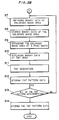
- Fig. 1 is a block diagram showing the structure of an image processing apparatus, to which a preferred embodiment of the present invention is applied.
- the image processing apparatus 110 comprises an image disc 111, a processing part 112 and a CPU 113.
- the image processing apparatus 110 first receives original image data D o of a line drawing from an input scanner 100.
- a variety of apparatuses such as a process scanner, a computer and the like, which generates the original image data D o , can be employed in place of the input scanner 100.
- the original image data D o which expresses shapes and densities of outlines in the line drawing, is stored in the image disc 111.
- the original image data D o is then transmitted from the image disc 111 to the processing part 112 to be subjected to data processing such as thinning processing on outline areas and processing for generating tint pattern data D t expressing tints to be laid on respective tint pattern areas.
- the tint pattern data D t is transmitted from the processing part 112 to the image disc 111 to be stored therein.
- the tint pattern data D t is then outputted from the image disc 111 to an output scanner 120, by which tint patterns are recorded as halftone positives or halftone negatives.
- the processing part 112 comprises an image memory 112a and a binary memory 112b.
- the image memory 112a temporarily stores a part of the original data D o to be processed in the processing part 112 and the binary memory 112b also temporarily stores binary data obtained through binarization of the original image data D o .
- the data processing in the processing part 112 is performed under the control by command signals delivered from the CPU 113.
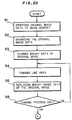
- Fig. 2 is a flow chart showing the procedure of the preferred embodiment of the present invention.
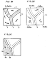
- Fig. 3 is a graph showing images at main steps of the preferred embodiments.
- an original image data D10 for an original image 10 shown in Fig. 3A is inputted from the image disc 111 to the image memory 112a at a step S1.
- the original image 10 has a shape of ten millimeter square, for example, and it is a part of a whole original image expressed by the original image data D o .
- the original image data D10 expresses the shape and the optical density of the line area 1.
- the original image 10 shown in Fig. 3A is an enlarged part of the whole original image and the line area 1 is consequently a part of outlines drawn on the whole original image.
- the original image may be either of a color picture and a line drawing of black and white.
- the original image data D10 is a density data assigned to each pixel for example.
- the original image data D10 is binarized by the CPU 113 at a step S2 with a prescribed threshold value. That is, if the density value of a pixel is higher than the threshold value, a binary data for the pixel is set at "1", and if the density value is lower than the threshold value, the binary data for the pixel is set at "0". If the image areas 2, 3 and 4 have their respective colors, the threshold value is set at a density higher than the respective colors and lower than that of the line area 1. Such a selection of the threshold value is possible since the line area 10 has been drawn with black or another deep color whose optical density is higher than those of the respective colors assigned to the areas 2, 3 and 4.
- the binary data B10 for the original image 10 thus obtained expresses the shape of the line area 1. If the original image data D10 itself is given as the binary data B10 and is transmitted from the image disc 111 to the image memory 112a at the step S1, the steps S2 is not necessary to be executed.
- the binary data B10 thus obtained is stored in both of the binary memory 112b and the image disc 111 at a step S3.
- the binary data B10 is subjected to a thinning process for reducing width of the line area 1 by a pixel width at a step S4.
- the thinning process will be described later in detail.
- a reduced binary data which expresses a shape of a reduced line area reduced by the pixel width from the line area 1, is obtained at the step S4.
- the binary data B10 stored in the binary memory 112b is replaced by the reduced binary data obtained at the step S4.
- the shape of the line area after the thinning process is compared with that before the thinning process at a step S6. If the shape of the line area is changed, the step S4 through S6 are excuted again. On the other hand, if the shape of the line area is found to be changed, the thinning process is ended. Consequently, binary data B 10a expressing an image 10a shown in Fig. 3B is obtained after repeating the steps S4-S6.
- the image 10a includes a thinned line area 1a whose width is equal to the pixel width, and enlarged image areas 2a, 3a and 4a which is expanded from the image areas 2, 3 and 4 shown in Fig. 3A.
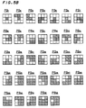
- the thinning process at the step S4 is performed with a (3 x 3) pixel cluster PC having nine pixels P0 through P8 as shown in Fig. 4.
- the center pixel P4 is sequentially positioned at each pixel in the original image 10, while performing logical processing on nine binary data assigned to the pixels P0 through P8 in the binary data B10 of the original image 10.
- the line area 1 is cut down by the pixel width ⁇ t at one side thereof.
- the width of the line area 1 is reduced by the pixel width ⁇ t after once of the thinning process at the step S4.
- the thinning process is repeated in order to reduce the line area 1 to the thinned line area 1a having the width equal to the pixel width ⁇ t.
- the content of the logical processing is determined under consideration of the following conditions:
- N1 a1 x INV(a3) x a4 x INV(a5) x a7
- N2 INV(a1) x a3 x a4 x a5 x INV(a7)
- N3 a1 x INV(a2) x INV(a3) x a4 x a5
- N4 a4 x a5 x a7 x INV(a8) x ⁇ INV(a1) + INV(a3) ⁇
- N5 INV(a1) x a3 x a4 x INV(a6)
- Fig. 5 is a schematic view showing patterns PA1-PA33 and PB1-PB33 of binary binary data in the pixel cluster PC, at which patterns the binary data a4 of the center pixel P4 is changed from "1" to "0” by the equations (1) and (3), respectively. Shaded pixels in the patterns PA1-PA33 and PB1-PB33 show that the initial binary data at the pixels are "1", and non-shaded pixels show that initial binary data at the pixels are "0". The shaded area is a part of the line area 1.
- the patterns PA1 through PA33 shown in Fig. 5A corresponds to the equation (1) and the patterns PB1 through PB33 shown in Fig. 5B corresponds to the equation (3).
- the equation (1) operates to eliminate the lower and right sides of the line area 1.
- the equation (3) operates to eliminate the upper left sides of the line area 1.
- the binary data a4 of the center pixel P4 is not changed by the equations (1) nor (3).
- a first logical processing with the equation (1) is first performed at the step S4, to thereby obtain a reduced binary data expressing a shape of a once-reduced line area whose width is reduced by the pixel width ⁇ t at the lower and right sides of the line area 1.
- a second logical processing with the equation (3) is performed, to thereby obtain a twice-reduced binary data expressing a shape of a twice-reduced line area whose width is reduced by the pixel width ⁇ t at the upper and left sides of the once-reduced line area.
- the first logical processing with the equation (1) and the second logical processing with the equation (3) are alternately performed at the step S4 until the thinned line area 1a having the pixel width ⁇ t is finally obtained.
- Fig. 6 is a view schematically showing the logical processing. If the pixel cluster PC is so positioned that the center pixel P4 is located at the edge of an initial area 5 as shown in Fig. 6A, the result of the first logical operation by the equation (1) becomes "0", whereby the binary data a4 of the center pixel P4 is replaced by the value of "0". After the first logical processing with the equation (1) for all the pixels included in the image, the right side of the line area 5 is eliminated. Then, the second logical processing with the equation (3) is performed. As a result, a thinned line area 5a of the pixel width ⁇ t is obtained as shown in Fig. 6B. However, segments 9a-9d remain in the enlarged image areas 2a, 3a and 4a shown in Fig. 3B at this time because of the condition C3 described before.
- binary data B 2a expressing a shape of the enlarged image area 2a is obtained.
- the image 10a shown in Fig. 3B is first displayed on image display means such as a cathode ray tube (CRT), then an operater designates one of the enlarged image areas 2a, 3a and 4a as a subject area with a stylus pen , a mouse or the like through pointing out some position in the enlarged image area 2a and specifies a color density of the designated image area 2a through inputting color density data with a keyboard or the like.
- image display means such as a cathode ray tube (CRT)
- an operater designates one of the enlarged image areas 2a, 3a and 4a as a subject area with a stylus pen , a mouse or the like through pointing out some position in the enlarged image area 2a and specifies a color density of the designated image area 2a through inputting color density data with a keyboard or the like.
- the processing part 112 recognizes that pixels having a value of "O" in the enlarged area 2a including the position pointed out by the operater and enclosed with the thinned line area 1a and the frame 11, are included in a single area.
- the binary data B 2a expressing the shape of the enlarged image area 2a shown in Fig. 3C is obtained. Namely, binary data of pixels included in the enlarged image area 2a are set at "1", and binary data of pixels out of the enlarged image area 2a in the image 10a are set at "O".
- binary data at the segments 9a and 9b which remain in the enlarged image area 2a as noise component and have values of "1" in the binary data B 10a at the step S4, are set at "O" in the binary data B 2a as noise component yet.
- the segments 9a and 9b are shown as non-shaded areas in Fig. 3c.
- the binary data B 2a is stored in the binary memory 112b at a step S8.
- logical processing is performed on the binary data B 2a for expanding the enlarged image area 2a by the pixel width ⁇ t toward the thinned line area 1a.
- Fig. 3D is an enlarged view showing the tint area 2b obtained through the expansion operation in the step S9.
- the expansion operation by the equation (5) so functions as to eliminate the segments 9a and 9b which remain in the enlarged image area 2a as noise component because the segments 9a and 9b are of the pixel width ⁇ t and are expressed with values of "O" in the binary data B 2a .
- binary data B 2b expressing the shape of the tint area 2b without the noise component is obtained at the step S9.
- the binary data B 2a stored in the binary memory 112b is replaced by the binary data B 2b for the tint area 2b at a step S10.
- tint-generation processing is performed on the binary data B 2b at a step S11.
- tint pattern data D 2b which expresses the shape and color of the tint area 2b, is generated on the basis of the binary data B 2b and a color density previously specified by an operator for the tint area 2b.
- the tint patter data D 2b thus obtained is stored in the image memory 112a at a step S12.
- tint pattern data D 3b for a tint area 3b shown in Fig. 3E is obtained at the steps S7 through S12 after returning to the step S7 from a step S13.
- the tint area 3b is an area expanded by a pixel width ⁇ t toward the thinned line area 1a from the enlarged image area 3a in the same way as that for the tint area 2b.
- the tint area 3b covers two parts 1c and 1d of the thinned line area 1a similarly to the tint area 2b.
- a part of the tint pattern data D 2b which corresponds to the part 1c of the thinned line area 1a included in both the tint areas 2b and 3b, is scratched and that part 1c is expressed by the tint pattern data D 3b which is generated later than the tint pattern data D 2b .
- the steps S7 through S13 are repeated in order to generate all the tint pattern data D 2b , D 3b and D 4b concerning the image areas 2, 3 and 4, which are all of the image area included in the original image 10 stored in the image memory 112a.
- Fig. 3F is a graph schematically showing final tint areas 2c, 3c and 4c expressed by final tint pattern data D 2c , D 3c and D 4c , respectively, which are finally obtained after the repetition of the steps S7 through S13.
- the final tint areas 2c, 3c and 4c are formed so as to contact each other and not to cause an overlap nor a blank between them.
- the final tint area 2c is the same with the enlarged image area 2a because two parts 1c and 1b of the thinned line area 1a included in the tint area 2b shown in Fig. 3D are expressed by the final pattern data D 3c and D 4c , respectively.
- the part 1c of the thinned line area 1a, which is positioned between the enlarged image area 2a and 3a is expressed by the final tint pattern data D 3c and the other part 1b of the thinned line area 1a is expressed by the final tint pattern data D 4c .
- the final tint pattern data D 4c is the same with the tint pattern data D 4b which is generated at the latest of all the tint pattern data D 2b , D 2c and D 4b .
- the final tint pattern data D 2c , D 3c and D 4c thus obtained are transmitted to the image disc 111 and stored therein at a step S14.
- the steps S1 through S14 are sequentially repeated for the other parts of the whole original image, whereby final tint pattern data concerning all of the image areas included in the whole original image are generated.
- the line area 1 is reduced to the thinned line area 1a having the width ⁇ t of one pixel.
- the line area 1 may be reduced to have a uniform width of N ⁇ t, where N is an integer, by the end of the step S6.
- final tint areas are also formed so as to contact each other and not to cause an overlap nor a blank between them if the amount of expansion at the step S9 is set at N ⁇ t.
- the amount of expansion may be set at a value of at leaset half of N ⁇ t in order for final tint areas to contact each other and not to cause an overlap nor a blank between them.
- blocks for the tint areas 2c, 3c and 4c are produced on the basis of the final tint pattern data D 2c , D 3c and D 4c , and a multicolor print with no line area of black color nor blank line is reproduced with the blocks.
- a multicolor print having the line area 1 of black color can be also reproduced through overprinting the line area 1, if necessary.
- image areas separated from each other with a line whose width is not constant can be easily transformed into tint areas contacting each other without casing an overlap nor a blank between them, and tint pattern data expressing respective shapes of the tint areas with prescribed colors can be easily generated.
Landscapes
- Engineering & Computer Science (AREA)
- Multimedia (AREA)
- Signal Processing (AREA)
- Editing Of Facsimile Originals (AREA)
- Image Processing (AREA)
- Facsimile Image Signal Circuits (AREA)
Applications Claiming Priority (2)
| Application Number | Priority Date | Filing Date | Title |
|---|---|---|---|
| JP63004698A JPH0693741B2 (ja) | 1988-01-14 | 1988-01-14 | 網伏せにおける画像整形方法 |
| JP4698/88 | 1988-01-14 |
Publications (3)
| Publication Number | Publication Date |
|---|---|
| EP0324506A2 true EP0324506A2 (fr) | 1989-07-19 |
| EP0324506A3 EP0324506A3 (en) | 1989-08-30 |
| EP0324506B1 EP0324506B1 (fr) | 1994-03-16 |
Family
ID=11591109
Family Applications (1)
| Application Number | Title | Priority Date | Filing Date |
|---|---|---|---|
| EP89100596A Expired - Lifetime EP0324506B1 (fr) | 1988-01-14 | 1989-01-13 | Procédé et appareil pour la génération de données de dessins dégradés |
Country Status (4)
| Country | Link |
|---|---|
| US (1) | US4922332A (fr) |
| EP (1) | EP0324506B1 (fr) |
| JP (1) | JPH0693741B2 (fr) |
| DE (1) | DE68913769T2 (fr) |
Cited By (3)
| Publication number | Priority date | Publication date | Assignee | Title |
|---|---|---|---|---|
| EP0391265A3 (fr) * | 1989-04-03 | 1991-03-13 | Honeywell Inc. | Procédé et appareil d'ombrage à densité linéaire variable pour un écran de cadre graphique |
| EP0397429A3 (fr) * | 1989-05-08 | 1992-01-29 | Canon Kabushiki Kaisha | Appareil et procédé de traitement d'images |
| US5206719A (en) * | 1989-05-10 | 1993-04-27 | Canon Kabushiki Kaisha | Image processing apparatus including means for extracting an outline |
Families Citing this family (16)
| Publication number | Priority date | Publication date | Assignee | Title |
|---|---|---|---|---|
| EP0398501B1 (fr) * | 1989-04-18 | 1996-09-04 | Canon Kabushiki Kaisha | Appareil de traitement d'images |
| JPH0831130B2 (ja) * | 1989-05-12 | 1996-03-27 | 大日本スクリーン製造株式会社 | 線画像の処理方法 |
| JP3152426B2 (ja) * | 1989-08-19 | 2001-04-03 | 株式会社リコー | 画像処理装置 |
| JP3056231B2 (ja) * | 1989-09-12 | 2000-06-26 | 株式会社リコー | 画像読取装置 |
| EP0463844B1 (fr) * | 1990-06-25 | 1997-06-04 | Canon Kabushiki Kaisha | Appareil et procédé de traitement d'images |
| US5289373A (en) * | 1991-11-29 | 1994-02-22 | General Electric Company | Method and apparatus for real-time tracking of catheter guide wires in fluoroscopic images during interventional radiological procedures |
| US5274551A (en) * | 1991-11-29 | 1993-12-28 | General Electric Company | Method and apparatus for real-time navigation assist in interventional radiological procedures |
| US5253169A (en) * | 1991-11-29 | 1993-10-12 | General Electric Company | Method and apparatus for reducing x-ray dosage during fluoroscopic examinations |
| US5537490A (en) * | 1992-06-04 | 1996-07-16 | Matsushita Electric Industrial Co., Ltd. | Line image processing method |
| JP3350822B2 (ja) * | 1992-08-04 | 2002-11-25 | アイシン精機株式会社 | 画像上のエッジ検出方法 |
| JPH08339449A (ja) * | 1995-04-11 | 1996-12-24 | Canon Inc | 画像処理装置及びその方法 |
| EP1345411B1 (fr) * | 2002-03-15 | 2018-11-21 | Canon Kabushiki Kaisha | Appareil et procédé de traitement d'images, et programme |
| JP3902967B2 (ja) * | 2002-03-15 | 2007-04-11 | キヤノン株式会社 | 画像処理装置、画像処理方法、プログラムおよび記憶媒体 |
| US7444141B2 (en) | 2003-06-12 | 2008-10-28 | Sergio Rivera | Method and system for programmable control of mobile communications units |
| JP5289066B2 (ja) * | 2009-01-05 | 2013-09-11 | キヤノン株式会社 | 画像処理方法、画像処理装置及びコンピュータプログラム |
| JP5543406B2 (ja) * | 2011-06-28 | 2014-07-09 | 京セラドキュメントソリューションズ株式会社 | 画像処理装置および画像形成装置 |
Family Cites Families (7)
| Publication number | Priority date | Publication date | Assignee | Title |
|---|---|---|---|---|
| US4204232A (en) * | 1977-07-08 | 1980-05-20 | Nippon Electric Co., Ltd. | Pattern transmission system comprising an encoder for encoding partial thinned patterns in two scanning lines along only one boundary line |
| GB2030823B (en) * | 1978-10-02 | 1982-11-03 | Ibm | Image data manipulation apparatus |
| JPS58127466A (ja) * | 1982-01-26 | 1983-07-29 | Fuji Xerox Co Ltd | 画像拡大縮小方式 |
| JPS5964846A (ja) * | 1982-10-05 | 1984-04-12 | Dainippon Screen Mfg Co Ltd | 絵柄と線画の同時記録方法 |
| JPS6165290A (ja) * | 1984-09-07 | 1986-04-03 | 株式会社日立製作所 | ベクトル文字フオントの作成装置 |
| JPS6180374A (ja) * | 1984-09-21 | 1986-04-23 | インタ−ナショナル ビジネス マシ−ンズ コ−ポレ−ション | 可変走査領域による細線化処理の方法及び装置 |
| JPS62216478A (ja) * | 1986-03-17 | 1987-09-24 | Dainippon Screen Mfg Co Ltd | 網ふせ装置 |
-
1988
- 1988-01-14 JP JP63004698A patent/JPH0693741B2/ja not_active Expired - Lifetime
-
1989
- 1989-01-13 EP EP89100596A patent/EP0324506B1/fr not_active Expired - Lifetime
- 1989-01-13 US US07/297,072 patent/US4922332A/en not_active Expired - Lifetime
- 1989-01-13 DE DE68913769T patent/DE68913769T2/de not_active Expired - Lifetime
Cited By (3)
| Publication number | Priority date | Publication date | Assignee | Title |
|---|---|---|---|---|
| EP0391265A3 (fr) * | 1989-04-03 | 1991-03-13 | Honeywell Inc. | Procédé et appareil d'ombrage à densité linéaire variable pour un écran de cadre graphique |
| EP0397429A3 (fr) * | 1989-05-08 | 1992-01-29 | Canon Kabushiki Kaisha | Appareil et procédé de traitement d'images |
| US5206719A (en) * | 1989-05-10 | 1993-04-27 | Canon Kabushiki Kaisha | Image processing apparatus including means for extracting an outline |
Also Published As
| Publication number | Publication date |
|---|---|
| US4922332A (en) | 1990-05-01 |
| DE68913769T2 (de) | 1994-07-28 |
| DE68913769D1 (de) | 1994-04-21 |
| JPH0693741B2 (ja) | 1994-11-16 |
| EP0324506B1 (fr) | 1994-03-16 |
| EP0324506A3 (en) | 1989-08-30 |
| JPH01181279A (ja) | 1989-07-19 |
Similar Documents
| Publication | Publication Date | Title |
|---|---|---|
| EP0324506A2 (fr) | Procédé et appareil pour la génération de données de dessins dégradés | |
| EP0322680B1 (fr) | Méthode et appareil pour corriger un patron de couleur dans un procédé multicolore | |
| US5048109A (en) | Detection of highlighted regions | |
| US5313570A (en) | Method for determining color boundaries for correcting for plate misregistration in color printing | |
| US5065437A (en) | Identification and segmentation of finely textured and solid regions of binary images | |
| EP0493962B1 (fr) | Procédé et appareil pour l'amélioration d'images des bits | |
| US5619592A (en) | Detection of highlighted regions | |
| EP0713329A1 (fr) | Procédé et appareil de segmentation automatique d'image par comparaison à des motifs standards | |
| US5359423A (en) | Method for statistical generation of density preserving templates for print enhancement | |
| EP0620534A1 (fr) | Procédé pour déterminer des bordures de couleur pour corriger une fausse régistration de plaque pour impression en couleur | |
| EP0618718A1 (fr) | Procédé et appareil pour corriger une fausse régistration de plaque pour impression en couleurs | |
| US5204918A (en) | Method of and apparatus for correcting contour of image | |
| EP0705024A2 (fr) | Procédé et appareil pour la génération d'images de séparation en couleurs | |
| KR950001543A (ko) | 화상 형성 장치 및 그 방법 | |
| US5724455A (en) | Automated template design method for print enhancement | |
| US5777758A (en) | Image processing apparatus and method for expanding color images based on block pixel and edge detection | |
| US4887228A (en) | Method for filling surface parts of an image with a surface pattern | |
| JP2003060918A (ja) | ランレングス符号化された画像データの形式で存在する印刷頁の色境界にトラッピングフレーム(3)を発生するための方法 | |
| JPH04296167A (ja) | デジタル中間調印刷装置 | |
| JPH07322057A (ja) | 2進入力画像の解像度の増大方法及びその増大装置、ならびに2進入力画像の外観の改良方法 | |
| EP0477904B1 (fr) | Méthode et appareil pour la génération d'images réduites | |
| EP0503606B1 (fr) | Procédé et appareil pour colorer une surface d'image | |
| EP0612182B1 (fr) | Processeur de conversion de format d'éléments d'images et de données pour gravure | |
| US7206463B2 (en) | Image processing method, device and system | |
| US5353359A (en) | Methods for generating character pattern data and making image |
Legal Events
| Date | Code | Title | Description |
|---|---|---|---|
| PUAI | Public reference made under article 153(3) epc to a published international application that has entered the european phase |
Free format text: ORIGINAL CODE: 0009012 |
|
| PUAL | Search report despatched |
Free format text: ORIGINAL CODE: 0009013 |
|
| AK | Designated contracting states |
Kind code of ref document: A2 Designated state(s): DE FR GB |
|
| AK | Designated contracting states |
Kind code of ref document: A3 Designated state(s): DE FR GB |
|
| 17P | Request for examination filed |
Effective date: 19891222 |
|
| 17Q | First examination report despatched |
Effective date: 19920513 |
|
| GRAA | (expected) grant |
Free format text: ORIGINAL CODE: 0009210 |
|
| AK | Designated contracting states |
Kind code of ref document: B1 Designated state(s): DE FR GB |
|
| PG25 | Lapsed in a contracting state [announced via postgrant information from national office to epo] |
Ref country code: FR Effective date: 19940316 |
|
| REF | Corresponds to: |
Ref document number: 68913769 Country of ref document: DE Date of ref document: 19940421 |
|
| EN | Fr: translation not filed | ||
| PLBE | No opposition filed within time limit |
Free format text: ORIGINAL CODE: 0009261 |
|
| STAA | Information on the status of an ep patent application or granted ep patent |
Free format text: STATUS: NO OPPOSITION FILED WITHIN TIME LIMIT |
|
| 26N | No opposition filed | ||
| REG | Reference to a national code |
Ref country code: GB Ref legal event code: IF02 |
|
| PGFP | Annual fee paid to national office [announced via postgrant information from national office to epo] |
Ref country code: DE Payment date: 20080110 Year of fee payment: 20 Ref country code: GB Payment date: 20080109 Year of fee payment: 20 |
|
| REG | Reference to a national code |
Ref country code: GB Ref legal event code: PE20 Expiry date: 20090112 |
|
| PG25 | Lapsed in a contracting state [announced via postgrant information from national office to epo] |
Ref country code: GB Free format text: LAPSE BECAUSE OF EXPIRATION OF PROTECTION Effective date: 20090112 |