EP0326822A2 - Baugruppe für datenverarbeitenden Schaltkreis - Google Patents
Baugruppe für datenverarbeitenden Schaltkreis Download PDFInfo
- Publication number
- EP0326822A2 EP0326822A2 EP89100441A EP89100441A EP0326822A2 EP 0326822 A2 EP0326822 A2 EP 0326822A2 EP 89100441 A EP89100441 A EP 89100441A EP 89100441 A EP89100441 A EP 89100441A EP 0326822 A2 EP0326822 A2 EP 0326822A2
- Authority
- EP
- European Patent Office
- Prior art keywords
- data device
- contact
- disposed
- module
- integrated circuit
- Prior art date
- Legal status (The legal status is an assumption and is not a legal conclusion. Google has not performed a legal analysis and makes no representation as to the accuracy of the status listed.)
- Granted
Links
Images
Classifications
-
- G—PHYSICS
- G06—COMPUTING OR CALCULATING; COUNTING
- G06K—GRAPHICAL DATA READING; PRESENTATION OF DATA; RECORD CARRIERS; HANDLING RECORD CARRIERS
- G06K19/00—Record carriers for use with machines and with at least a part designed to carry digital markings
- G06K19/06—Record carriers for use with machines and with at least a part designed to carry digital markings characterised by the kind of the digital marking, e.g. shape, nature, code
- G06K19/067—Record carriers with conductive marks, printed circuits or semiconductor circuit elements, e.g. credit or identity cards also with resonating or responding marks without active components
- G06K19/07—Record carriers with conductive marks, printed circuits or semiconductor circuit elements, e.g. credit or identity cards also with resonating or responding marks without active components with integrated circuit chips
- G06K19/077—Constructional details, e.g. mounting of circuits in the carrier
- G06K19/07745—Mounting details of integrated circuit chips
- G06K19/07747—Mounting details of integrated circuit chips at least one of the integrated circuit chips being mounted as a module
-
- G—PHYSICS
- G06—COMPUTING OR CALCULATING; COUNTING
- G06K—GRAPHICAL DATA READING; PRESENTATION OF DATA; RECORD CARRIERS; HANDLING RECORD CARRIERS
- G06K19/00—Record carriers for use with machines and with at least a part designed to carry digital markings
- G06K19/06—Record carriers for use with machines and with at least a part designed to carry digital markings characterised by the kind of the digital marking, e.g. shape, nature, code
- G06K19/067—Record carriers with conductive marks, printed circuits or semiconductor circuit elements, e.g. credit or identity cards also with resonating or responding marks without active components
- G06K19/07—Record carriers with conductive marks, printed circuits or semiconductor circuit elements, e.g. credit or identity cards also with resonating or responding marks without active components with integrated circuit chips
- G06K19/077—Constructional details, e.g. mounting of circuits in the carrier
- G06K19/07745—Mounting details of integrated circuit chips
Definitions
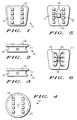
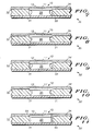
- Module 10 consists of a contact carrier 11 having a plurality of contacts 12 disposed thereon.
- the bottom of contact carrier 11 is illustrated in FIGS. 5 and 6.
- FIG. 6 a contact arrangement is shown that permits flip chip bonding of die 13 to contacts 12.
- Die 13 is bonded to conductive lines 15 which are disposed on the bottom of carrier 11 and coupled to contacts 12.
Landscapes
- Engineering & Computer Science (AREA)
- Computer Hardware Design (AREA)
- Microelectronics & Electronic Packaging (AREA)
- Physics & Mathematics (AREA)
- General Physics & Mathematics (AREA)
- Theoretical Computer Science (AREA)
- Credit Cards Or The Like (AREA)
Applications Claiming Priority (2)
| Application Number | Priority Date | Filing Date | Title |
|---|---|---|---|
| US150811 | 1988-02-01 | ||
| US07/150,811 US4943708A (en) | 1988-02-01 | 1988-02-01 | Data device module having locking groove |
Publications (3)
| Publication Number | Publication Date |
|---|---|
| EP0326822A2 true EP0326822A2 (de) | 1989-08-09 |
| EP0326822A3 EP0326822A3 (en) | 1990-05-30 |
| EP0326822B1 EP0326822B1 (de) | 1994-06-08 |
Family
ID=22536088
Family Applications (1)
| Application Number | Title | Priority Date | Filing Date |
|---|---|---|---|
| EP89100441A Expired - Lifetime EP0326822B1 (de) | 1988-02-01 | 1989-01-12 | Baugruppe für datenverarbeitenden Schaltkreis |
Country Status (4)
| Country | Link |
|---|---|
| US (1) | US4943708A (de) |
| EP (1) | EP0326822B1 (de) |
| JP (1) | JP2717432B2 (de) |
| DE (1) | DE68915797T2 (de) |
Cited By (10)
| Publication number | Priority date | Publication date | Assignee | Title |
|---|---|---|---|---|
| FR2660092A1 (fr) * | 1990-03-26 | 1991-09-27 | Ryoden Kasei Kk | Procede de fabrication d'une carte a circuit integre. |
| DE9100665U1 (de) * | 1991-01-21 | 1992-07-16 | TELBUS Gesellschaft für elektronische Kommunikations-Systeme mbH, 85391 Allershausen | Trägerelement für integrierte Halbleiter-Schaltkreise, insbesondere zum Einbau in Chip-Karten |
| WO1994022110A1 (fr) * | 1993-03-18 | 1994-09-29 | Droz Francois | Procede de fabrication d'une carte comprenant au moins un element electronique et carte obtenue par un tel procede |
| WO1994022111A1 (fr) * | 1993-03-17 | 1994-09-29 | Droz Francois | Procede de fabrication d'une carte comprenant au moins un element electronique |
| FR2703489A1 (fr) * | 1993-03-30 | 1994-10-07 | Droz Francois | Procédé de fabrication d'une carte comprenant au moins un élément électronique et carte obtenue par un tel procédé. |
| WO1995001612A1 (en) * | 1993-07-02 | 1995-01-12 | Gec Avery Limited | An integrated circuit card |
| WO1995033246A1 (fr) * | 1994-05-27 | 1995-12-07 | Ake Gustafson | Procede de realisation d'un module electronique et module electronique obtenu selon ce procede |
| WO1998015916A1 (de) * | 1996-10-09 | 1998-04-16 | Pav Card Gmbh | Verfahren und verbindungsanordnung zum herstellen einer chipkarte |
| WO1999035611A1 (de) * | 1998-01-09 | 1999-07-15 | Siemens Aktiengesellschaft | Trägerelement für einen halbleiterchip |
| FR2792091A1 (fr) * | 1999-04-12 | 2000-10-13 | Schlumberger Systems & Service | Carte a memoire electronique securisee |
Families Citing this family (14)
| Publication number | Priority date | Publication date | Assignee | Title |
|---|---|---|---|---|
| JPH0271676U (de) * | 1988-11-21 | 1990-05-31 | ||
| US6016255A (en) * | 1990-11-19 | 2000-01-18 | Dallas Semiconductor Corp. | Portable data carrier mounting system |
| US6122704A (en) * | 1989-05-15 | 2000-09-19 | Dallas Semiconductor Corp. | Integrated circuit for identifying an item via a serial port |
| US5229641A (en) * | 1989-11-25 | 1993-07-20 | Hitachi Maxell, Ltd. | Semiconductor card and manufacturing method therefor |
| US5374818A (en) * | 1992-03-09 | 1994-12-20 | Control Module Inc. | Identification means with integral memory device |
| US5786988A (en) * | 1996-07-02 | 1998-07-28 | Sandisk Corporation | Integrated circuit chips made bendable by forming indentations in their back surfaces flexible packages thereof and methods of manufacture |
| FR2756648B1 (fr) * | 1996-11-29 | 1999-01-08 | Solaic Sa | Carte a memoire du type sans contact |
| US7158008B2 (en) * | 2002-03-29 | 2007-01-02 | Datakey Electronincs, Inc. | Electronic key system and method |
| CN101816010A (zh) * | 2007-07-19 | 2010-08-25 | 数据匙电子有限公司 | Rf令牌和接纳器系统与方法 |
| USD649894S1 (en) * | 2008-12-30 | 2011-12-06 | Atek Products, Llc | Electronic token and data carrier |
| WO2010088556A1 (en) | 2009-01-30 | 2010-08-05 | Datakey Electronics, Inc. | Data carrier system having a compact footprint and methods of manufacturing the same |
| USD649896S1 (en) | 2009-01-30 | 2011-12-06 | Atek Products, Llc | Electronic token and data carrier receptacle |
| USD649895S1 (en) | 2009-01-30 | 2011-12-06 | Atek Products, Llc | Electronic token and data carrier |
| USD649486S1 (en) | 2009-07-09 | 2011-11-29 | ATEK Products , LLC | Electronic token and data carrier |
Family Cites Families (13)
| Publication number | Priority date | Publication date | Assignee | Title |
|---|---|---|---|---|
| US4167605A (en) * | 1975-07-29 | 1979-09-11 | Imperial Chemical Industries Limited | Article with antistick coating and composition |
| FR2483657B1 (fr) * | 1980-05-30 | 1986-11-21 | Bull Sa | Machine portable pour le calcul ou le traitement de l'information |
| DE3029939A1 (de) * | 1980-08-07 | 1982-03-25 | GAO Gesellschaft für Automation und Organisation mbH, 8000 München | Ausweiskarte mit ic-baustein und verfahren zu ihrer herstellung |
| DE3153768C2 (de) * | 1981-04-14 | 1995-11-09 | Gao Ges Automation Org | Ausweiskarte |
| FR2526977B1 (fr) * | 1982-05-14 | 1988-06-10 | Cii Honeywell Bull | Procede et dispositif pour authentifier ou certifier au moins une information contenue dans une memoire d'un support electronique notamment amovible et portatif tel qu'une carte |
| US4448630A (en) * | 1982-07-13 | 1984-05-15 | Philippe Blanquart | Machine for applying a film |
| JPS60217491A (ja) * | 1984-04-12 | 1985-10-31 | Dainippon Printing Co Ltd | Icカ−ドの製造法 |
| JPH0353328Y2 (de) * | 1984-11-05 | 1991-11-21 | ||
| DE3689094T2 (de) * | 1985-07-27 | 1994-03-10 | Dainippon Printing Co Ltd | IC-Karte. |
| JPS62140896A (ja) * | 1985-12-13 | 1987-06-24 | 日本写真印刷株式会社 | Icカ−ドの製造方法 |
| US4755661A (en) * | 1986-01-10 | 1988-07-05 | Ruebsam Herrn H | Connection of electronic components in a card |
| JPS6395995A (ja) * | 1986-10-13 | 1988-04-26 | 芝 悦嗣 | チツプ埋込みプラスチツクカ−ドの製造方法 |
| FR2609821B1 (fr) * | 1987-01-16 | 1989-03-31 | Flonic Sa | Procede de realisation de cartes a memoire et cartes obtenues par la mise en oeuvre dudit procede |
-
1988
- 1988-02-01 US US07/150,811 patent/US4943708A/en not_active Expired - Lifetime
-
1989
- 1989-01-12 DE DE68915797T patent/DE68915797T2/de not_active Expired - Fee Related
- 1989-01-12 EP EP89100441A patent/EP0326822B1/de not_active Expired - Lifetime
- 1989-01-31 JP JP1022470A patent/JP2717432B2/ja not_active Expired - Fee Related
Cited By (17)
| Publication number | Priority date | Publication date | Assignee | Title |
|---|---|---|---|---|
| US5346576A (en) * | 1990-03-26 | 1994-09-13 | Mitsubishi Denki Kabushiki Kaisha | Method of manufacturing IC card |
| FR2660092A1 (fr) * | 1990-03-26 | 1991-09-27 | Ryoden Kasei Kk | Procede de fabrication d'une carte a circuit integre. |
| DE9100665U1 (de) * | 1991-01-21 | 1992-07-16 | TELBUS Gesellschaft für elektronische Kommunikations-Systeme mbH, 85391 Allershausen | Trägerelement für integrierte Halbleiter-Schaltkreise, insbesondere zum Einbau in Chip-Karten |
| WO1994022111A1 (fr) * | 1993-03-17 | 1994-09-29 | Droz Francois | Procede de fabrication d'une carte comprenant au moins un element electronique |
| FR2703490A1 (fr) * | 1993-03-17 | 1994-10-07 | Droz Francois | Procédé de fabrication d'une carte comprenant au moins un élément électronique. |
| US5585618A (en) * | 1993-03-18 | 1996-12-17 | Droz; Fran+525 Ois | Method of manufacture of a card comprising at least one electronic element and card obtained by such method |
| WO1994022110A1 (fr) * | 1993-03-18 | 1994-09-29 | Droz Francois | Procede de fabrication d'une carte comprenant au moins un element electronique et carte obtenue par un tel procede |
| AU670497B2 (en) * | 1993-03-18 | 1996-07-18 | Nagraid S.A. | Method for producing a card with at least one electronic component, and card thereby obtained |
| FR2703489A1 (fr) * | 1993-03-30 | 1994-10-07 | Droz Francois | Procédé de fabrication d'une carte comprenant au moins un élément électronique et carte obtenue par un tel procédé. |
| WO1995001612A1 (en) * | 1993-07-02 | 1995-01-12 | Gec Avery Limited | An integrated circuit card |
| WO1995033246A1 (fr) * | 1994-05-27 | 1995-12-07 | Ake Gustafson | Procede de realisation d'un module electronique et module electronique obtenu selon ce procede |
| AU684174B2 (en) * | 1994-05-27 | 1997-12-04 | Assa Abloy Ab | Method for fabricating an electronic module and electronic module obtained thereby |
| US5879502A (en) * | 1994-05-27 | 1999-03-09 | Gustafson; Ake | Method for making an electronic module and electronic module obtained according to the method |
| WO1998015916A1 (de) * | 1996-10-09 | 1998-04-16 | Pav Card Gmbh | Verfahren und verbindungsanordnung zum herstellen einer chipkarte |
| WO1999035611A1 (de) * | 1998-01-09 | 1999-07-15 | Siemens Aktiengesellschaft | Trägerelement für einen halbleiterchip |
| FR2792091A1 (fr) * | 1999-04-12 | 2000-10-13 | Schlumberger Systems & Service | Carte a memoire electronique securisee |
| EP1045338A1 (de) * | 1999-04-12 | 2000-10-18 | SCHLUMBERGER Systèmes | Elektronische Speicherkarte mit Kartensicherheitselement |
Also Published As
| Publication number | Publication date |
|---|---|
| EP0326822A3 (en) | 1990-05-30 |
| DE68915797T2 (de) | 1994-12-22 |
| US4943708A (en) | 1990-07-24 |
| DE68915797D1 (de) | 1994-07-14 |
| EP0326822B1 (de) | 1994-06-08 |
| JPH02147296A (ja) | 1990-06-06 |
| JP2717432B2 (ja) | 1998-02-18 |
Similar Documents
| Publication | Publication Date | Title |
|---|---|---|
| US4943708A (en) | Data device module having locking groove | |
| US5673179A (en) | Plastic integrated circuit card with reinforcement structure outer to the card and protecting integrated circuit module | |
| RU2667741C1 (ru) | Способ встраивания интегральной схемы методом перевернутого кристалла | |
| US4755661A (en) | Connection of electronic components in a card | |
| US5877941A (en) | IC card and method of fabricating the same | |
| KR102883917B1 (ko) | 직물에 스마트 카드를 연결하기 위한 장치 및 플렉시블 스마트 카드 형식의 전자 카드 제조 방법 | |
| JP3505238B2 (ja) | 情報記憶担体及びその製造方法 | |
| JPS62290594A (ja) | Icカード | |
| JPS6227195A (ja) | Icカ−ドおよびicモジュール | |
| KR100293418B1 (ko) | 비접촉식 아이씨 카드 제조 방법 | |
| JPS633998A (ja) | Icカ−ド | |
| JPS62268693A (ja) | Icカ−ド及びその製造方法 | |
| JPH0230598A (ja) | Icモジュールおよびicカード | |
| EP4174719A1 (de) | Kontaktloses modul ohne leitungsrahmen | |
| JPS60142489A (ja) | Icカ−ド | |
| JPH072225Y2 (ja) | Icカード | |
| JPS6337429B2 (de) | ||
| JPS62227797A (ja) | Icカ−ド | |
| JPS6282093A (ja) | 磁気ストライプ付icカ−ド | |
| JPH084310Y2 (ja) | Icカード | |
| JPH03202397A (ja) | Icカード | |
| JPS6377792A (ja) | 薄型電子機器 | |
| JPH06143885A (ja) | Icカードのモジュール構造 | |
| JPS63257694A (ja) | Icカ−ドの製造方法 | |
| JPH05291469A (ja) | 樹脂封止型半導体装置、この樹脂封止型半導体装置を用いたメモリカードおよびその製造方法 |
Legal Events
| Date | Code | Title | Description |
|---|---|---|---|
| PUAI | Public reference made under article 153(3) epc to a published international application that has entered the european phase |
Free format text: ORIGINAL CODE: 0009012 |
|
| AK | Designated contracting states |
Kind code of ref document: A2 Designated state(s): DE FR GB |
|
| PUAL | Search report despatched |
Free format text: ORIGINAL CODE: 0009013 |
|
| AK | Designated contracting states |
Kind code of ref document: A3 Designated state(s): DE FR GB |
|
| 17P | Request for examination filed |
Effective date: 19901123 |
|
| 17Q | First examination report despatched |
Effective date: 19930114 |
|
| GRAA | (expected) grant |
Free format text: ORIGINAL CODE: 0009210 |
|
| AK | Designated contracting states |
Kind code of ref document: B1 Designated state(s): DE FR GB |
|
| REF | Corresponds to: |
Ref document number: 68915797 Country of ref document: DE Date of ref document: 19940714 |
|
| ET | Fr: translation filed | ||
| PLBE | No opposition filed within time limit |
Free format text: ORIGINAL CODE: 0009261 |
|
| STAA | Information on the status of an ep patent application or granted ep patent |
Free format text: STATUS: NO OPPOSITION FILED WITHIN TIME LIMIT |
|
| 26N | No opposition filed | ||
| PGFP | Annual fee paid to national office [announced via postgrant information from national office to epo] |
Ref country code: GB Payment date: 19971229 Year of fee payment: 10 |
|
| PGFP | Annual fee paid to national office [announced via postgrant information from national office to epo] |
Ref country code: FR Payment date: 19980116 Year of fee payment: 10 |
|
| PGFP | Annual fee paid to national office [announced via postgrant information from national office to epo] |
Ref country code: DE Payment date: 19980120 Year of fee payment: 10 |
|
| PG25 | Lapsed in a contracting state [announced via postgrant information from national office to epo] |
Ref country code: GB Free format text: LAPSE BECAUSE OF NON-PAYMENT OF DUE FEES Effective date: 19990112 |
|
| GBPC | Gb: european patent ceased through non-payment of renewal fee |
Effective date: 19990112 |
|
| PG25 | Lapsed in a contracting state [announced via postgrant information from national office to epo] |
Ref country code: FR Free format text: LAPSE BECAUSE OF NON-PAYMENT OF DUE FEES Effective date: 19990930 |
|
| PG25 | Lapsed in a contracting state [announced via postgrant information from national office to epo] |
Ref country code: DE Free format text: LAPSE BECAUSE OF NON-PAYMENT OF DUE FEES Effective date: 19991103 |
|
| REG | Reference to a national code |
Ref country code: FR Ref legal event code: ST |