EP0351867A2 - Elektrolumineszierende Anordnung von Verbindungshalbleitern - Google Patents
Elektrolumineszierende Anordnung von Verbindungshalbleitern Download PDFInfo
- Publication number
- EP0351867A2 EP0351867A2 EP89113441A EP89113441A EP0351867A2 EP 0351867 A2 EP0351867 A2 EP 0351867A2 EP 89113441 A EP89113441 A EP 89113441A EP 89113441 A EP89113441 A EP 89113441A EP 0351867 A2 EP0351867 A2 EP 0351867A2
- Authority
- EP
- European Patent Office
- Prior art keywords
- conductive layer
- zns
- light
- impurity element
- substrate
- Prior art date
- Legal status (The legal status is an assumption and is not a legal conclusion. Google has not performed a legal analysis and makes no representation as to the accuracy of the status listed.)
- Granted
Links
Images



Classifications
-
- H—ELECTRICITY
- H10—SEMICONDUCTOR DEVICES; ELECTRIC SOLID-STATE DEVICES NOT OTHERWISE PROVIDED FOR
- H10H—INORGANIC LIGHT-EMITTING SEMICONDUCTOR DEVICES HAVING POTENTIAL BARRIERS
- H10H20/00—Individual inorganic light-emitting semiconductor devices having potential barriers, e.g. light-emitting diodes [LED]
- H10H20/80—Constructional details
- H10H20/81—Bodies
- H10H20/816—Bodies having carrier transport control structures, e.g. highly-doped semiconductor layers or current-blocking structures
- H10H20/8162—Current-blocking structures
-
- G—PHYSICS
- G09—EDUCATION; CRYPTOGRAPHY; DISPLAY; ADVERTISING; SEALS
- G09F—DISPLAYING; ADVERTISING; SIGNS; LABELS OR NAME-PLATES; SEALS
- G09F13/00—Illuminated signs; Luminous advertising
- G09F13/20—Illuminated signs; Luminous advertising with luminescent surfaces or parts
- G09F13/22—Illuminated signs; Luminous advertising with luminescent surfaces or parts electroluminescent
-
- G—PHYSICS
- G09—EDUCATION; CRYPTOGRAPHY; DISPLAY; ADVERTISING; SEALS
- G09F—DISPLAYING; ADVERTISING; SIGNS; LABELS OR NAME-PLATES; SEALS
- G09F13/00—Illuminated signs; Luminous advertising
- G09F13/20—Illuminated signs; Luminous advertising with luminescent surfaces or parts
- G09F13/22—Illuminated signs; Luminous advertising with luminescent surfaces or parts electroluminescent
- G09F2013/222—Illuminated signs; Luminous advertising with luminescent surfaces or parts electroluminescent with LEDs
-
- H—ELECTRICITY
- H10—SEMICONDUCTOR DEVICES; ELECTRIC SOLID-STATE DEVICES NOT OTHERWISE PROVIDED FOR
- H10H—INORGANIC LIGHT-EMITTING SEMICONDUCTOR DEVICES HAVING POTENTIAL BARRIERS
- H10H20/00—Individual inorganic light-emitting semiconductor devices having potential barriers, e.g. light-emitting diodes [LED]
- H10H20/052—Light-emitting semiconductor devices having Schottky type light-emitting regions; Light emitting semiconductor devices having Metal-Insulator-Semiconductor type light-emitting regions
-
- H—ELECTRICITY
- H10—SEMICONDUCTOR DEVICES; ELECTRIC SOLID-STATE DEVICES NOT OTHERWISE PROVIDED FOR
- H10H—INORGANIC LIGHT-EMITTING SEMICONDUCTOR DEVICES HAVING POTENTIAL BARRIERS
- H10H20/00—Individual inorganic light-emitting semiconductor devices having potential barriers, e.g. light-emitting diodes [LED]
- H10H20/80—Constructional details
- H10H20/81—Bodies
- H10H20/822—Materials of the light-emitting regions
- H10H20/823—Materials of the light-emitting regions comprising only Group II-VI materials, e.g. ZnO
- H10H20/8232—Materials of the light-emitting regions comprising only Group II-VI materials, e.g. ZnO characterised by the dopants
-
- H—ELECTRICITY
- H10—SEMICONDUCTOR DEVICES; ELECTRIC SOLID-STATE DEVICES NOT OTHERWISE PROVIDED FOR
- H10H—INORGANIC LIGHT-EMITTING SEMICONDUCTOR DEVICES HAVING POTENTIAL BARRIERS
- H10H29/00—Integrated devices, or assemblies of multiple devices, comprising at least one light-emitting semiconductor element covered by group H10H20/00
- H10H29/10—Integrated devices comprising at least one light-emitting semiconductor component covered by group H10H20/00
- H10H29/14—Integrated devices comprising at least one light-emitting semiconductor component covered by group H10H20/00 comprising multiple light-emitting semiconductor components
- H10H29/142—Two-dimensional arrangements, e.g. asymmetric LED layout
-
- H—ELECTRICITY
- H10—SEMICONDUCTOR DEVICES; ELECTRIC SOLID-STATE DEVICES NOT OTHERWISE PROVIDED FOR
- H10W—GENERIC PACKAGES, INTERCONNECTIONS, CONNECTORS OR OTHER CONSTRUCTIONAL DETAILS OF DEVICES COVERED BY CLASS H10
- H10W72/00—Interconnections or connectors in packages
- H10W72/071—Connecting or disconnecting
- H10W72/075—Connecting or disconnecting of bond wires
- H10W72/07551—Connecting or disconnecting of bond wires characterised by changes in properties of the bond wires during the connecting
- H10W72/07554—Connecting or disconnecting of bond wires characterised by changes in properties of the bond wires during the connecting changes in dispositions
-
- H—ELECTRICITY
- H10—SEMICONDUCTOR DEVICES; ELECTRIC SOLID-STATE DEVICES NOT OTHERWISE PROVIDED FOR
- H10W—GENERIC PACKAGES, INTERCONNECTIONS, CONNECTORS OR OTHER CONSTRUCTIONAL DETAILS OF DEVICES COVERED BY CLASS H10
- H10W72/00—Interconnections or connectors in packages
- H10W72/50—Bond wires
- H10W72/531—Shapes of wire connectors
- H10W72/536—Shapes of wire connectors the connected ends being ball-shaped
-
- H—ELECTRICITY
- H10—SEMICONDUCTOR DEVICES; ELECTRIC SOLID-STATE DEVICES NOT OTHERWISE PROVIDED FOR
- H10W—GENERIC PACKAGES, INTERCONNECTIONS, CONNECTORS OR OTHER CONSTRUCTIONAL DETAILS OF DEVICES COVERED BY CLASS H10
- H10W72/00—Interconnections or connectors in packages
- H10W72/50—Bond wires
- H10W72/541—Dispositions of bond wires
- H10W72/547—Dispositions of multiple bond wires
-
- Y—GENERAL TAGGING OF NEW TECHNOLOGICAL DEVELOPMENTS; GENERAL TAGGING OF CROSS-SECTIONAL TECHNOLOGIES SPANNING OVER SEVERAL SECTIONS OF THE IPC; TECHNICAL SUBJECTS COVERED BY FORMER USPC CROSS-REFERENCE ART COLLECTIONS [XRACs] AND DIGESTS
- Y10—TECHNICAL SUBJECTS COVERED BY FORMER USPC
- Y10S—TECHNICAL SUBJECTS COVERED BY FORMER USPC CROSS-REFERENCE ART COLLECTIONS [XRACs] AND DIGESTS
- Y10S428/00—Stock material or miscellaneous articles
- Y10S428/901—Printed circuit
-
- Y—GENERAL TAGGING OF NEW TECHNOLOGICAL DEVELOPMENTS; GENERAL TAGGING OF CROSS-SECTIONAL TECHNOLOGIES SPANNING OVER SEVERAL SECTIONS OF THE IPC; TECHNICAL SUBJECTS COVERED BY FORMER USPC CROSS-REFERENCE ART COLLECTIONS [XRACs] AND DIGESTS
- Y10—TECHNICAL SUBJECTS COVERED BY FORMER USPC
- Y10S—TECHNICAL SUBJECTS COVERED BY FORMER USPC CROSS-REFERENCE ART COLLECTIONS [XRACs] AND DIGESTS
- Y10S428/00—Stock material or miscellaneous articles
- Y10S428/917—Electroluminescent
Definitions
- the present invention relates to electroluminescent devices of compound semiconductor, and more particulary to improvements in electroluminescent devices comprising a Group II - VI compound semiconductor such as zinc sulfide (ZnS) or zinc selenide (ZnSe).
- a Group II - VI compound semiconductor such as zinc sulfide (ZnS) or zinc selenide (ZnSe).
- Group II - VI compound semiconductors such as ZnS and ZnSe are generally used as materials for devices, such as blue light-emitting diodes, for producing light with high efficiency over the region of ultraviolet rays to visible rays.
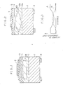
- Fig. 14 shows an example of structure conventionally used for electroluminescent devices of such a Group II - VI compound semiconductor.
- Indicated at 71 is a low-resistance n-type ZnS single-crystal substrate prepared from a ZnS bulk single crystal grown by the halogen chemical transport process, by heat-treating the crystal in molten zinc at 1000 o C for 100 hours.
- a light-emitting layer 74 of n-type ZnS and an insulating layer 75 of insulating ZnS are successively formed epitaxially over the substrate 71 by molecular beam epitaxy (MBE) or organometallic chemical vapor deposition (MOCVD).
- MBE molecular beam epitaxy
- MOCVD organometallic chemical vapor deposition
- Gold (Au) is deposited on the insulating layer 75 by vacuum evaporation to form a positive electrode 77.
- An ohmic electrode of indium (In) serving as a negative electrode 78 is formed on the rear surface of the low-resistance n-type substrate 71.
- a MIS electroluminescent device is fabricated.
- an electroluminescent device wherein a conductive layer is provided between a substrate and a light-emitting layer.
- the proposed device comprises a low-resistance n-type ZnS substrate 83 having a resistivity of 10 to 1 ohm-cm and a thickness of 300 to 1000 ⁇ m, a low-resistance n-type ZnS conductive layer 84 having a resistivity of 10 ⁇ 2 to 10 ⁇ 3 ohm-cm and epitaxially formed over the substrate 83, for example, by MBE from ZnS with Al, Cl or the like added thereto, a low-resistance n-type ZnS light-emitting layer 85 and a ZnS high-resistance layer 86 which are formed successivesively over the layer 84, for example, by MBE, an ohmic electrode 82 formed on the rear surface of the substrate 83 by depositing In thereon by vacuum evaporation and heat-treating the deposit in a high-purity gas atmosphere at 450 o C for several seconds to several minutes, an electrode 87 formed on the high-
- the current injected via the electrodes 77, 78 or 82, 88 flows through the device over a wide region, so that the current density in the light-emitting layer 74 or 85 is small. This makes it difficult to obtain luminescence with high brightness. Furthermore, the light produced by the emitting layer 74 or 85 radiates through the device in every direction. It is therefore likely that the light produced will not be taken out of the device efficiently.
- Either one of the foregoing constructions of electroluminescent devices may be used for fabricating a monolithic display device which comprises a multiplicity of minute luminescent chips having a unit size of 100 ⁇ m and prepared by forming a minute discrete pattern on the substrate.
- a monolithic display device which comprises a multiplicity of minute luminescent chips having a unit size of 100 ⁇ m and prepared by forming a minute discrete pattern on the substrate.
- An object of the present invention which has been accomplished in view of the foregoing situation, is to provide an electroluminescent device of Group II - VI compound semiconductor adapted to produce light with high brightness.
- the present invention provides an electroluminescent device of compound semiconductor which comprises an electroluminescent device body formed on a substrate and providing a light-emitting portion and a conductive portion joined to the lower surface and/or the upper surface of the light-emitting portion, and a pair of electrodes for applying therethrough an external voltage to the body to cause electroluminescence, the conductive portion comprising a conductive layer formed of a Group II - VI compound semiconductor made to have a substantially low resistance by the addition of an impurity element, and a conductive layer part provided in the conductive layer and formed of a Group II - VI compound semiconductor having a higher refractive index than the Group II - VI compound semiconductor of the conductive layer and containing an impurity element added thereto, the conductive layer part being so shaped as to confine thereto the light produced by the light-emitting portion.
- the present invention provides an electro luminescent device of Group II - VI compound semiconductor which comprises a substrate, a light-emitting portion, and a conductive portion provided at least between the substrate and the light-emitting portion for injecting into the light-emitting portion the current to be produced in the device by the application of an external voltage.
- the conductive portion comprises a conductive layer formed of a Group II - VI compound semiconductor made to have a substantially low resistance by the addition of an impurity element, and a conductive layer part provided in the conductive layer and formed of a Group II - VI compound semiconductor having an impurity element added thereto.
- the Group II - VI compound semiconductor used for forming the conductive layer part is made to have a higher refractive index than the semiconductor forming the conductive layer. Consequently, the light produced by the light-emitting portion can be confined to the layer part having the higher refractive index and delivered from the device efficiently with high brightness.
- the conductive layer part when shaped, for example, in the form of a lens, renders the light produced by the emitting portion convergent or directional, making it possible to deliver the light from the device toward a specified direction more efficiently.
- the electroluminescent device of the present invention is prepared from a Group II - VI compound semiconductor.
- the light emitted by the light-emitting portion by the application of a voltage across the electrodes has a multiplicity of colors including blue and appears on the upper surface or lower surface of the device.
- the device is used as a light source having high energy and high brightness for various displays, printers, facsimile systems, etc.
- the conductive portion joined to the lower surface and/or the upper surface of the light-emitting portion comprises a conductive layer (hereinafter referred to as the "first conductive layer”) and a conductive layer part (hereinafter referred to as the "second conductive layer”) provided in the first conductive layer, and that the Group II - VI compound semiconductor forming the second conductive layer has a higher refractive index than the semiconductor forming the first conductive layer.
- the substrate for use in the invention is preferably made of a Group II - VI compound semiconductor.
- Examples of such semiconductors are low-resistance n-type ZnS, low-resistance n-type ZnSe, low-resistance n-type ZnS x Se 1-x and the like, and insulating ZnS, insulating ZnSe, insulating ZnS x Se 1-x and the like.
- the substrate of low-resistance n-type ZnS (or low-resistance n-type ZnSe or low-resistance n-type ZnS x Se 1-x ) is prepared from a ZnS bulk single crystal (or ZnSe bulk single crystal or ZnS x Se 1-x bulk single crystal) grown by the halogen chemical transport process, by heat-treating the single crystal in molten zinc at 1000 o C for about 100 hours.
- the substrate thus obtained is made to have a low resistance.
- the above materials forming the substrate have the following resistivities (ohm-cm).
- ZnS x Se 1-x 1 to 10, more preferably about 1.
- n-type impurities useful for the heat treatment in preparing the substrates are Al, Ga and the like, Cl and Br. Also usable are In, I and the like.
- a ZnS bulk single crystal or ZnSe bulk single crystal or ZnS x Se 1-x bulk single crystal
- the substrate obtained is colored yellow or orange and is low in transparency for the luminescence wavelength, so that the blue light produced, for example, needs to be taken out from the semiconductor side.
- the Zn S 0.5 Se 0.5 crystal which is grown by the sublimation process, the resulting substrate is almost colorless and transparent and is desirable since blue light emitted can be taken out also from the substrate side.
- the substrate to be used in this case need not be subjected to the low-resistance treatment conventionally employed, but the wafer obtained from a bulk single crystal can be used as it is, i.e., with its high resistivity (with insulating to semi-insulating property, 106 to 1015 ohm-cm).
- the light-emitting portion to be formed in the present invention is preferably an n-type ZnS light-emitting layer providing a ZnS electroluminescent device of the MIS (metal insulator semiconductor) type, or a light-emitting layer having a p-n junction provided by the combination of n-type ZnSe and p-type ZnSe for constituting a p-n junction electroluminescent device of the planar structure type.
- the Group II - VI compound semiconductor for the light-emitting layer is not limited to ZnS; also usable is, for example, ZnSe, ZnS x Se 1-x or ZnS y Te 1-y .
- ZnSe p-n junction is not limitative; also usable are ZnS p-n junction, ZnS x Se 1-x p-n junction, ZnS y Te 1-y p-n junction, p-n heterojunctions afforded by such materials, and various other junctions.
- the first conductive layer which is made to have a substantially low resistance by the addition of impurity means one having a resistivity of 1 to 10 ⁇ 2 ohm-cm.
- This resistivity is controllable by setting the concentration of impurity added to 1016 to 1018 at.cm ⁇ 3, whereby the electric resistance is settable to the range useful for electroluminescent devices.
- the conductive portion comprises an n-type first conductive layer formed on a Group II - VI compound semiconductor, such as ZnS, ZnSe or ZnS x Se 1-x , having substantially low resistance, and an n-type second conductive layer provided in the first layer and formed of a Group II - VI compound semiconductor different in kind or composition from the semiconductor of the first layer and having a higher refractive index than the semiconductor of the first conductive layer.
- ZnS and ZnSe are 2.4 and 2.7, respectively, in refractive index.
- ZnS x Se 1-x which is a mixed crystal of these, is controllable in refractive index between the above values by varying the S content (x) thereof.
- the second conductive layer have a higher refractive index than the first. For this purpose, it is desired to make the sulfur (S) content (x) of the second conductive layer at least about 0.5 greater than that of the first conductive layer.
- the first and second conductive layers is 1018 to 1019 cm 3 in electron concentration and as low as 5 x 10 ⁇ 2 to 5 x 10 ⁇ 3 in resistivity. Further preferably, the second conductive layer is lower than the first in resistivity.
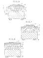
- the second conductive layer is in the form of a solid cylinder (see Figs. 1, 4, 5 and 6) or a Fresnel lens including a convex lens (see Figs. 2 and 8), or is trapezoidal in section (see Fig. 7).
- the cylindrical layer is about 30 to about 100 ⁇ m in diameter and about 5 to about 20 ⁇ m in thickness (preferably 10 ⁇ m).
- composition of the second conductive layer may be uniform or may vary continuously or stepwise from each of the upper and lower interfaces between the first and second conductive layers toward the center of the second widthwise thereof (see Fig. 6).
- n-type impurities for use in preparing the first and second conductive layers and the light-emitting layer are elements from Group III such as boron (B), aluminum (Al), gallium (Ga), indium (In) and thallium (Tl), and elements from Group VII such as chlorine (Cl), bromine (Br), fluorine (F) and iodine (I). At least one of these elements is used, or at least one of such elements from Group III is used in combination with at least one of these elements from Group VII.
- examples of useful p-type impurities are elements from Group Ia such as lithium (Li), sodium (Na), potassium (K), rubidium (Rb) and cesium (Cs), the elements from Group Ib, i.e. copper (Cu), silver (Ag) and Gold (Au), thallium from Group III and elements from Group V such as nitrogen (N), phosphorus (P), arsenic (As), antimony (Sb) and bismuth (Bi). At least one of these elements is used, or at least one of the above elements from Group Ia or Ib is used in combination with at least one element from Group V.
- These impurities are suitable for giving epitaxial films which are small in the degree of compensation and have a high quality.
- epitaxial compound semiconductor layers are formed one over another on the compound semiconductor substrate to form the body of an electroluminescent device.
- the device body usually measures 50 to 500 ⁇ m in width, 80 to 800 ⁇ m in length and 2 to 15 ⁇ m in thickness.
- the device body may be formed singly on the substrate, or a multiplicity of device bodies can be formed in a scattered arrangement to provide a monolithic electroluminescent display or a large-area electroluminescent display. Fig.
- FIG. 13 shows a monolithic electroluminescent display including compound semiconductor electroluminescent devices 58 each having an insulating ZnSe substrate 51, an electroluminescent device body formed on the substrate 51 and comprising a p-type ZnSe conductive layer 52, a p-type ZnSe light-emitting layer 53, an n-type ZnSe light-emitting layer 54 and an n-type ZnSe conductive layer 55 (a conductive layer portion provided in the conductive layer 55 and having a higher n-type impurity concentration than the layer 55 is not shown, the same as hereinafter) which are formed one over another, an Au positive electrode 56 provided on the conductive layer 52, and an In negative electrode 57 provided on the conductive layer 55 forming the uppermost layer of the device body.
- compound semiconductor electroluminescent devices 58 each having an insulating ZnSe substrate 51, an electroluminescent device body formed on the substrate 51 and comprising a p
- the device 58 on the substrate measures 450 ⁇ m in width H and 750 ⁇ m in length M.
- the display has 24 x 24 electroluminescent devices as arranged separately from one another in the form of a matrix. An arrangement of such displays provides a large-area electroluminescent display apparatus.
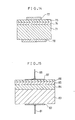
- Fig. 9 shows a MIS-type electroluminescent device 60 having a high-resistance layer formed on a light-emitting layer. More specifically, the device 60 comprises an insulating ZnS substrate 61, a device body formed on the substrate and having an n-type ZnS conductive layer 62 and an n-type ZnS light-emitting layer 63 on the layer 62, a ZnS high-resistance layer 64 formed on the light-emitting layer 63, an Au positive electrode 65 provided on the layer 64, and an In negative electrode 66 provided on the conductive layer 62. Indicated at 65a and 66a are lead wires.
- Fig. 10 shows an electroluminescent device 90 of the p-n junction type.
- the device 90 comprises an insulating ZnSe substrate 91, a device body formed on the substrate and comprising an n-type ZnSe conductive layer 92, an n-type ZnSe light-emitting layer 93, a p-type ZnSe light-emitting layer 94 and a p-type ZnSe conductive layer 95 which are formed one over another, an Au positive electrode 96 provided on the conductive layer 95, and an In negative electrode 97 provided on the conductive layer 92. Indicated at 96a and 97a are lead wires.
- the electrode 66, 65 or 97, 96 are arranged respectively in an electrode forming space on the conductive layer and on the uppermost layer of the device body (on the conductive layer 55 in Fig. 13, on the high-resistance layer 64 in Fig. 9, or on the conductive layer 95 in Fig. 10) for applying a voltage therethrough to the device body.
- the voltage which would otherwise be applied via the substrate can be efficiently applied to the device body. This precludes the loss due to the substrate to result in the following advantages.
- Such a compound semiconductor electroluminescent device is fabricated by placing a mask having a specified rectangular aperture on a high-resistance compound semiconductor substrate, for example of 106 to 1015 ohm-cm, forming a low-resistance semiconductor conductive layer as the lowermost layer first on the substrate, and forming a compound semiconductor light-emitting layer, and a compound semiconductor light-resistance layer or a compound semiconductor conductive layer as superposed layers on the resulting conductive layer except at an electrode forming site.
- the layers are formed, for example, by MBE.
- the device is prepared in this way by one of the following two processes.
- the first of the processes comprises placing a mask of thin metal film having at least one specified rectangular aperture on the compound semiconductor substrate, epitaxially growing a compound semiconductor conductive layer first as the lowermost layer, then shifting the mask so as to cover the electrode forming site on the layer with the mask, forming a compound semiconductor light-emitting layer on the conductive layer, further epitaxially growing a compound semiconductor high-resistance layer or compound semiconductor conductive layer on the light-emitting layer to obtain a device body, removing the mask and thereafter providing electrodes at the electrode forming site on the lowermost
- the second process comprises placing a mask of thin metal film having at least one specified rectangular aperture over the compound semiconductor substrate at a specified distance (which is usually 10 to 500 ⁇ m to be suitable) away therefrom, epitaxially growing a compound semiconductor conductive layer first, then altering the angle of inclination of the substrate provided with the mask (generally suitably by 5 to 45 degrees) with respect to the direction of projection of the molecular beam to mask an electrode forming site on the conductive layer, forming a compound semiconductor light-emitting layer on the conductive layer, further epitaxially growing a compound semiconductor high-resistance layer or compound semiconductor conductive layer on the resulting layer to obtain a device body, removing the mask and providing electrodes at the electrode forming site on the lowermost conductive layer and on the surface of the uppermost high-resistance layer or conductive layer.
- the electroluminescent device body thus obtained comprises epitaxial compound semiconductor layers which are all identical in shape when seen from above. It is suitable that the electrode forming site on the lowermost layer be usually 5 to 80% of the surface of the lowermost layer in area.
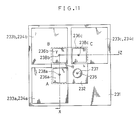
- Figs. 11 and 12 show a ZnS multicolor electroluminescent device of the MIS-type similar to the one shown in Fig. 9.
- the device comprises a semi-insulating (high-resistance) ZnS substrate 231, a low-resistance n-type epitaxial ZnS conductive layer 232, low-resistance n-type epitaxial ZnS light-emitting layers 233a, 233b, 233c, hole injecting epitaxial ZnS high-resistance layers 234a, 234b, 234c, an ohmic metal (In) electrode 235 formed on the conductive layer 232, metal (Au) electrodes 236a, 236b, 236c formed on the respective high-resistance layers 234a, 234b, 234c and metal lead wires 237, 238a, 238b, 238c.
- This device is prepared by placing a mask of thin metal plate having a rectangular aperture on the semi-insulating (high-resistance) ZnS substrate 231, growing the conductive layer 232 by MBE, thereafter growing the light-emitting layer 233a and the high-resistance layer 234a in overlapping relation with the conductive layer 232 by MBE with the mask shifted to form a light-emitting portion A, similarly forming light-emitting portions B and C in succession with the mask further shifted, and providing the electrodes 235, 236a, 236b and 236c.
- the device thus formed includes the three light-emitting portions A, B and C having the conductive layer 232 in common.
- the light-emitting layers of the respective light-emitting portions have added thereto as impurities Al and Ag at about one-tenth the concentration of Al, Al and Cu at about one-tenth the concentration of Al, and Al and cadmium (Cd) at one-half the concentration of Al, respectively.
- the second conductive layer is formed during the growth of the first conductive layer by locally irradiating the grown layer, for example, with ArF excimer laser beam at a wavelength of 193 nm, whereby impurities are added at a high concentration to the irradiated portion of the grown layer, consequently forming a region having an impurity concentration which is greater than that of the non-irradiated portion by about one order of magnitude. This region provides the second conductive layer.
- Fig. 1 shows an electroluminescent device as a first embodiment of the invention.
- Indicated at 1 is a substrate of n-type ZnS single crystal.
- a low-resistance n-type ZnS layer and a low-resistance n-type zinc sulfo-selenide (ZnS x Se 1-x ) lyaer are grown on the substrate 1 continuously epitaxially.
- the alloy layer is then etched away as by chemical etching or reactive ion etching (RIE) except for the portion thereof under the light-emitting portion to be formed.
- RIE reactive ion etching
- a low-resistance n-type ZnS layer is then grown again to form a first conductive layer 2 of n-type ZnS and a second conductive layer 131 of n-type ZnS x Se 1-x as positioned in the first conductive layer 2.
- ZnS has a refractive index of 2.4. According to the sulfur (S) content (x), the refractive index of ZnS x Se 1-x continuously varies from the refractive index of ZnS, 2.4, to the refractive index of ZnSe, 2.7.
- the second layer 131 is higher than the first layer 2 in refractive index.
- a light-emitting layer 4 of n-type ZnS and an insulating layer 5 of insulating ZnS are formed over the first conductive layer 2.
- a positive electrode 7 is formed on the insulating layer 5 by depositing Au by vacuum evaporation.
- An ohmic In electrode serving as a negative electrode 8 is formed on the rear surface of the substrate 1.
- the semiconductor layers are epitaxially grown by MBE or MOCVD. In fact, each layer was grown by either process with good controllability by varying the amount of material to be fed and changing the material.
- the ZnS insulating layer can be obtained without addition of impurities. However, if it is likely that high-resistance n-type ZnS will be formed with a low insulating property, highly insulating ZnS can be formed with addition of at least one of the following impurity elements for forming p-type ZnS, i.e., lithium, sodium, potassium, rubidium and cesium from Group Ia, copper, silver and gold from Group Ib, and nitrogen, phosphorus arsenic, antimony and bismuth from Group V. At least one of such elements from Groups IA, Ib and V is also usable in combination with at least one of elements from Groups III and VII.
- the first and second conductive layers 2, 131 are set to a low resistivity (e.g. 5 x 10 ⁇ 2 to 5 x 10 ⁇ 3 ohm-cm), with their impurity concentration set to about 1018 to 1019 cm ⁇ 3.
- the second layer 131 is made lower than the first layer 2 in resistivity, thereby permitting current to pass chiefly through the second layer 131 and to flow into the light-emitting layer 4 at a high density, whereby blue light can be produced with high brightness.
- the S content is set to not higher than 0.5.
- the layer 131 is about 10 ⁇ m in thickness so that the light emitted by the emitting layer can be directed toward the substrate efficiently.
- the portions of the first conductive layer 2 positioned on and beneath the second layer 131 are each about 2 ⁇ m in thickness to diminish the strain of each interface between the layers 2 and 131.
- the layer is formed of n-type ZnS having high crystallinity and a lower electron concentration of about 1017 cm ⁇ 3 than the conductive layers and is about 1 to about 5 ⁇ m in thickness.
- the insulating layer 5 has a small thickness of 20 to 700 angstroms to assure the highest current injection efficiency.
- the positive electrode 7 is made to have a thickness of 2000 to 3000 angstroms so that the light emitted upward from the emitting layer can be totally reflected toward the substrate.
- the electrode is positioned immediately above the second conductive layer 131.
- the negative electrode 8 is formed in an annular shape so that blue light produced can be delivered from the rear side of the substrate.
- the light emitted by the emitting layer 4 is confined to the second conductive layer 131 of higher refractive index when passing through the first conductive layer 2 and can be delivered from the substrate side efficiently.
- the embodiment realizes a ZnS MIS-type blue electroluminescent device with a delivery efficiency which is one order of magnitude greater than heretofore possible.
- a light-emitting layer of p-type ZnS with a hole concentration of 1014 to 1017 cm ⁇ 3 can be formed in place of the insulating layer 5 over the light-emitting layer 4 of n-type ZnS.
- the ZnS p-n junction electroluminescent device thus realized achieves a delivery efficiency which is about one order of magnitude greater than is achieved by conventional p-n junction or ⁇ -n junction devices.
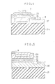
- Fig. 2 shows a second embodiment of the invention, i.e., another ZnS MIS-type electroluminescent device wherein the second conductive layer 131 is in the form of a convex lens.
- Each of the layers shown is grown by MOCVD using a beam having greater energy than the band gap width of ZnS or ZnS x Se 1-x to be grown, such as an ArF excimer laser beam at a wavelength of 193 nm or monochromatic light released from a xenon lamp having a spectral output of 50 mW/nm/cm2.
- the contemplated layer can be fully grown even at a low growth temperature (200 to 350 o C) at which little or no growth occurs (not greater than 0.001 ⁇ m/h) in the usual case wherein no light is applied.
- the rate of growth is controllable over a wide range of about 0.01 ⁇ m/h to about 10 ⁇ m/h by varying the intensity of beam.
- a conductive portion is formed by this beam grown method.
- low-resistance n-type ZnS is grown on a low-resistance n-type ZnS substrate 1 by the application of a beam with an intensity distribution represented by solid line A in Fig. 3, to form the lower segment 12a of a first conduc tive layer which has a central concave portion and which measures about 2 ⁇ m at the central portion and about 7 ⁇ m at the end portion in thickness.
- low-resistance n-type ZnS x Se 1-x is grown by the application of a beam with an intensity distribution represented by broken line B in Fig.
- n-type ZnS is thereafter grown using the same beam as used for forming the lower segment 12a to form the upper segment 12b of the first conductive layer.
- An n-type ZnS light-emitting layer 4 and an insulating layer 5 of insulating ZnS are then formed over the first conductive layer thus obtained, followed by the formation of a positive electrode 7 on the insulating layer 5 and a negative electrode 8 on the rear surface of the substrate 1. In this way, a ZnS MIS-type electroluminescent device is fabricated.
- the second conductive layer 131 which has a higher refractive index than the first conductive layer segments 12a, 12b, is in the form of a convex lens, with the result that the light produced by the emitting layer 4 can be rendered convergent and directional and can therefore be delivered from the device toward the desired direction with an improved efficiency.
- Fig. 4 schematically shows a third embodiment of the present invention.
- an insulating ZnS x Se 1-x 21a is prepared from a ZnS x Se 1-x bulk single crystal grown by the halogen chemical transport process without subjecting the crystal to low-resistance treatment.
- Formed over the substrate are a first conductive layer 32 of low-resistance n-type ZnS y Se 1-y , and a second conductive layer 33 of low-resistance n-type ZnSe having a higher refractive index than the first layer 32.
- ZnS y Se 1-y forming the first conductive layer 32 is given a sulfur content (y) of at least 0.5 so that the second conductive layer has a sufficiently higher refractive index than the first layer 32.
- a light-emitting layer 24 of n-type ZnSe and a light-emitting layer 25 of p-type ZnSe are formed over the conductive portion.
- An Au ohmic electrode is formed on the layer 25 as a positive electrode 7.
- These light-emitting layers are locally etched away to expose the first conductive layer 32, and an In ohmic electrode is provided on the exposed surface as a negative electrode 8.
- a p-n junction electroluminescent device is obtained.
- the substrate 21a has a wider band gap than the ZnSe light-emitting layers 24, 25 and causes not re-absorption, while the device is of planar structure and therefore has no electrode on the rear side of the substrate 21a.
- the present embodiment affords a ZnSe p-n junction electroluminescent device which achieves a still improved light delivery efficiency.
- Fig. 5 schematically shows a fourth embodiment of the invention.
- an insulating ZnSe substrate 21 is prepared from a ZnSe bulk sing!e crystal grown by the halogen chemical transport process without subjecting the crystal to low-resistance treatment.
- Epitaxially grown over the substrate 21 are a conductive layer 38 of low-resistance p-type ZnSe, a p-type ZnSe light-emitting layer 25, and an n-type ZnSe light-emitting layer 24.
- a first conductive layer 32 made of low-resistance n-type ZnS y Se 1-y and having a thickness of 10 ⁇ m is thereafter formed, with a second conductive layer 133 of low-resistance ZnS k Se 1-k (k ⁇ y) formed in the layer 32.
- An In negative electrode 8 is formed on the first conductive layer 32.
- the conductive layer 38 is locally etched away, and an Au positive electrode 7 is formed on the exposed surface of the layer 38.
- a p-n junction electroluminescent device is obtained.
- the sulfur content (y) of ZnS y Se 1-y forming the first conductive layer 32 should be greater than k + 0.5 so that the second conductive layer 133 of ZnS k Se 1-k has a sufficiently higher refractive index than the first conductive layer 32.
- the first and second conductive layers are formed on or above the light-emitting layers, with the result that the light produced from the emitting layers can be deliverd from the upper surface of the device efficiently.
- Fig. 6 shows a fifth embodiment of the invention.
- this embodiment has the same construction as the ZnS MIS-type devices already described except that the second conductive layer 43 is formed of n-type ZnS x (l)Se 1-x (l) (l: distance from the bottom face 43a of the layer 43 toward the direction of its thickness, i.e. direction Y) wherein the sulfur (S) content/selenium (Se) content ratio varies continuously or stepwise in the direction Y.
- the composition of the second conductive layer 43 continuously varies from ZnS to ZnS x Se 1-x , from each interface between the layers 2 and 43 widthwise of the layer 43. This completely inhibits the defect that would occur at the interface due to the difference in lattice constant between the layers.
- the present embodiment realizes electroluminescent devices of the ZnS MIS type or p-n junction type having a high light delivery efficiency.
- Fig. 7 schematically shows a sixth embodiment of the invention.
- this embodiment basically has the same construction as the ZnS MIS-type device described above except that the second conductive layer 131 has a trapezoidal section and a thickness which decreases at its opposite ends toward the direction of its width.
- a low-resistance n-type ZnS layer and a low-resistance ZnS x Se 1-x are successively epitaxially grown over a low-resistance n-type ZnS substrate 1, the latter layer is then etched to form the trapezoidal layer 131, and low-resistance n-type ZnS is epitaxially grown again to complete a first conductive layer 2.
- the second conductive layer 131 has a higher refractive index than the first conductive layer 2.
- the light incident on each end portion of the second conductive layer 131 where the interface between the two layers 2, 131 is inclined with respect to the light-emitting layer 4 is refracted toward the center.
- the light emanating from the light-emitting layer 4 can therefore be converged toward the substrate 1. This achieves a greatly improved delivery efficiency.
- the present embodiment realizes ZnS MIS-type or p-n junction electroluminescent devices exhibiting a further improved delivery efficiency.
- the second conductive layers of the devices according to the third, fourth and fifth embodiments can be made trapezoidal as is the case with the present embodiment, whereby a converging property can be given to the light emanating from the light-emitting layer, thereby enabling the device to deliver the light efficiently.
- Fig. 8 shows a seventh embodiment of the invention.
- the second conductive layer 131 of this embodiment is in the form of a Fresnel lens, which gives a high converging property and high directionality to the light produced by the light-emitting layer 4.
- the device fabricated is therefore adapted to deliver the light toward the desired direction with a high efficiency.
- the foregoing first to seventh embodiments realize efficient compound semiconductor electroluminescent devices which are greatly improved in the convergence and directionality of light and light delivery efficiency and which are very useful as light sources for various optoelectronic apparatus such as high-brightness blue electroluminescent displays for use in displaying and processing data.
Landscapes
- Physics & Mathematics (AREA)
- General Physics & Mathematics (AREA)
- Engineering & Computer Science (AREA)
- Theoretical Computer Science (AREA)
- Led Devices (AREA)
- Electroluminescent Light Sources (AREA)
- Physical Deposition Of Substances That Are Components Of Semiconductor Devices (AREA)
- Semiconductor Lasers (AREA)
Applications Claiming Priority (4)
| Application Number | Priority Date | Filing Date | Title |
|---|---|---|---|
| JP182664/88 | 1988-07-21 | ||
| JP18266488A JP2708183B2 (ja) | 1988-07-21 | 1988-07-21 | 化合物半導体発光素子 |
| JP63240556A JPH0287685A (ja) | 1988-07-21 | 1988-09-26 | 化合物半導体発光素子 |
| JP240556/88 | 1988-09-26 |
Publications (3)
| Publication Number | Publication Date |
|---|---|
| EP0351867A2 true EP0351867A2 (de) | 1990-01-24 |
| EP0351867A3 EP0351867A3 (de) | 1991-10-16 |
| EP0351867B1 EP0351867B1 (de) | 1994-09-21 |
Family
ID=26501383
Family Applications (3)
| Application Number | Title | Priority Date | Filing Date |
|---|---|---|---|
| EP89113443A Expired - Lifetime EP0351869B1 (de) | 1988-07-21 | 1989-07-21 | Elektrolumineszierende Anordnung von Verbindungshalbleitern |
| EP89113441A Expired - Lifetime EP0351867B1 (de) | 1988-07-21 | 1989-07-21 | Elektrolumineszierende Anordnung von Verbindungshalbleitern |
| EP89113442A Expired - Lifetime EP0351868B1 (de) | 1988-07-21 | 1989-07-21 | Elektrolumineszierende Anordnung von Verbindungshalbleitern |
Family Applications Before (1)
| Application Number | Title | Priority Date | Filing Date |
|---|---|---|---|
| EP89113443A Expired - Lifetime EP0351869B1 (de) | 1988-07-21 | 1989-07-21 | Elektrolumineszierende Anordnung von Verbindungshalbleitern |
Family Applications After (1)
| Application Number | Title | Priority Date | Filing Date |
|---|---|---|---|
| EP89113442A Expired - Lifetime EP0351868B1 (de) | 1988-07-21 | 1989-07-21 | Elektrolumineszierende Anordnung von Verbindungshalbleitern |
Country Status (4)
| Country | Link |
|---|---|
| US (3) | US4988579A (de) |
| EP (3) | EP0351869B1 (de) |
| JP (5) | JP2708183B2 (de) |
| DE (3) | DE68918362T2 (de) |
Cited By (5)
| Publication number | Priority date | Publication date | Assignee | Title |
|---|---|---|---|---|
| US5103269A (en) * | 1989-07-10 | 1992-04-07 | Sharp Kabushiki Kaisha | Electroluminescent device of compound semiconductor comprising zns or zns and znse |
| WO1996011498A1 (en) * | 1994-10-11 | 1996-04-18 | International Business Machines Corporation | Monolithic array of light emitting diodes for the generation of light at multiple wavelengths and its use for multicolor display applications |
| WO2002033756A1 (de) * | 2000-10-16 | 2002-04-25 | Osram Opto Semiconductors Gmbh | Led-modul |
| CN105849796A (zh) * | 2013-12-27 | 2016-08-10 | 株式会社半导体能源研究所 | 发光装置 |
| CN109346497A (zh) * | 2018-09-26 | 2019-02-15 | 北京蜃景光电科技有限公司 | 微显示器件及其制备方法、显示面板 |
Families Citing this family (44)
| Publication number | Priority date | Publication date | Assignee | Title |
|---|---|---|---|---|
| JPH0268968A (ja) * | 1988-09-02 | 1990-03-08 | Sharp Corp | 化合物半導体発光素子 |
| DE68928245T2 (de) * | 1988-12-27 | 1997-12-11 | Canon Kk | Durch elektrisches Feld lichtemittierende Vorrichtung |
| US5198690A (en) * | 1990-11-26 | 1993-03-30 | Sharp Kabushiki Kaisha | Electroluminescent device of II-IV compound semiconductor |
| JP2593960B2 (ja) * | 1990-11-29 | 1997-03-26 | シャープ株式会社 | 化合物半導体発光素子とその製造方法 |
| US5252895A (en) * | 1991-05-09 | 1993-10-12 | Westinghouse Electric Corp. | TFEL edge emitter structure with light emitting face at angle greater than ninety degrees to substrate street |
| US5291507A (en) * | 1991-05-15 | 1994-03-01 | Minnesota Mining And Manufacturing Company | Blue-green laser diode |
| CN1119358A (zh) * | 1991-05-15 | 1996-03-27 | 明尼苏达州采矿制造公司 | 蓝-绿激光二极管 |
| US5274269A (en) * | 1991-05-15 | 1993-12-28 | Minnesota Mining And Manufacturing Company | Ohmic contact for p-type group II-IV compound semiconductors |
| US5404027A (en) * | 1991-05-15 | 1995-04-04 | Minnesota Mining & Manufacturing Compay | Buried ridge II-VI laser diode |
| US5183689A (en) * | 1991-07-15 | 1993-02-02 | Cvd, Inc. | Process for an improved laminated of znse and zns |
| JP2837004B2 (ja) * | 1991-09-30 | 1998-12-14 | 株式会社デンソー | Elディスプレイ素子 |
| JPH05182766A (ja) * | 1991-12-26 | 1993-07-23 | Toyota Central Res & Dev Lab Inc | 薄膜el素子 |
| US5536584A (en) * | 1992-01-31 | 1996-07-16 | Hitachi, Ltd. | Polyimide precursor, polyimide and metalization structure using said polyimide |
| AU4104293A (en) * | 1992-05-19 | 1993-12-13 | California Institute Of Technology | Wide band-gap semiconductor light emitters |
| WO1994015369A1 (en) * | 1992-12-22 | 1994-07-07 | Research Corporation Technologies, Inc. | Group ii-vi compound semiconductor light emitting devices and an ohmic contact therefor |
| JPH06196261A (ja) * | 1992-12-25 | 1994-07-15 | Hitachi Maxell Ltd | 薄膜型エレクトロルミネツセンス素子 |
| US5459337A (en) * | 1993-02-19 | 1995-10-17 | Sony Corporation | Semiconductor display device with red, green and blue emission |
| US5422902A (en) * | 1993-07-02 | 1995-06-06 | Philips Electronics North America Corporation | BeTe-ZnSe graded band gap ohmic contact to p-type ZnSe semiconductors |
| US5445550A (en) * | 1993-12-22 | 1995-08-29 | Xie; Chenggang | Lateral field emitter device and method of manufacturing same |
| JP3156503B2 (ja) | 1994-05-27 | 2001-04-16 | 松下電器産業株式会社 | 固体撮像装置の駆動方法及び固体撮像装置の信号処理回路 |
| US5796120A (en) * | 1995-12-28 | 1998-08-18 | Georgia Tech Research Corporation | Tunnel thin film electroluminescent device |
| JP2839027B2 (ja) * | 1997-01-23 | 1998-12-16 | 住友電気工業株式会社 | Ii−vi族化合物半導体の熱処理方法 |
| JP3934730B2 (ja) * | 1997-03-28 | 2007-06-20 | ローム株式会社 | 半導体発光素子 |
| US5889364A (en) * | 1997-08-22 | 1999-03-30 | Durel Corporation | Electrical, solderless snap connector for EL lamp |
| JP2001267085A (ja) * | 2000-03-23 | 2001-09-28 | Sanyo Electric Co Ltd | 有機発光装置およびその製造方法 |
| US7064355B2 (en) * | 2000-09-12 | 2006-06-20 | Lumileds Lighting U.S., Llc | Light emitting diodes with improved light extraction efficiency |
| JP2002141556A (ja) | 2000-09-12 | 2002-05-17 | Lumileds Lighting Us Llc | 改良された光抽出効果を有する発光ダイオード |
| US7053419B1 (en) | 2000-09-12 | 2006-05-30 | Lumileds Lighting U.S., Llc | Light emitting diodes with improved light extraction efficiency |
| US6650044B1 (en) * | 2000-10-13 | 2003-11-18 | Lumileds Lighting U.S., Llc | Stenciling phosphor layers on light emitting diodes |
| US6987613B2 (en) * | 2001-03-30 | 2006-01-17 | Lumileds Lighting U.S., Llc | Forming an optical element on the surface of a light emitting device for improved light extraction |
| DE10120703A1 (de) * | 2001-04-27 | 2002-10-31 | Osram Opto Semiconductors Gmbh | Halbleiterchip für die Optoelektronik |
| JP3758562B2 (ja) * | 2001-11-27 | 2006-03-22 | 日亜化学工業株式会社 | 窒化物半導体多色発光素子 |
| JP2005026688A (ja) * | 2003-06-30 | 2005-01-27 | Osram Opto Semiconductors Gmbh | 放射放出半導体チップ、該半導体チップの作製方法および該半導体チップの明るさの調整設定方法 |
| US7009213B2 (en) | 2003-07-31 | 2006-03-07 | Lumileds Lighting U.S., Llc | Light emitting devices with improved light extraction efficiency |
| US7151338B2 (en) * | 2003-10-02 | 2006-12-19 | Hewlett-Packard Development Company, L.P. | Inorganic electroluminescent device with controlled hole and electron injection |
| JP2005123526A (ja) * | 2003-10-20 | 2005-05-12 | Oki Data Corp | 半導体装置、ledヘッド、及び画像形成装置 |
| DE102004029412A1 (de) * | 2004-02-27 | 2005-10-13 | Osram Opto Semiconductors Gmbh | Strahlungsemittierender Halbleiterchip und Verfahren zur Herstellung eines solchen Halbleiterchips |
| US7419839B2 (en) | 2004-11-12 | 2008-09-02 | Philips Lumileds Lighting Company, Llc | Bonding an optical element to a light emitting device |
| US7462502B2 (en) * | 2004-11-12 | 2008-12-09 | Philips Lumileds Lighting Company, Llc | Color control by alteration of wavelength converting element |
| WO2007091500A1 (en) * | 2006-02-10 | 2007-08-16 | Semiconductor Energy Laboratory Co., Ltd. | Light emitting element, light emitting device, and electronic device |
| JP5300345B2 (ja) | 2007-08-10 | 2013-09-25 | キヤノン株式会社 | 発光膜、発光素子およびその製造方法 |
| US9337407B2 (en) * | 2009-03-31 | 2016-05-10 | Epistar Corporation | Photoelectronic element and the manufacturing method thereof |
| KR100986440B1 (ko) * | 2009-04-28 | 2010-10-08 | 엘지이노텍 주식회사 | 발광소자 및 그 제조방법 |
| US20120097918A1 (en) * | 2010-10-20 | 2012-04-26 | Varian Semiconductor Equipment Associates, Inc. | Implanted current confinement structure to improve current spreading |
Family Cites Families (16)
| Publication number | Priority date | Publication date | Assignee | Title |
|---|---|---|---|---|
| US3919589A (en) * | 1973-04-06 | 1975-11-11 | Rca Corp | Electroluminescent cell with a current-limiting layer of high resistivity |
| JPS5437800B2 (de) * | 1973-06-19 | 1979-11-16 | ||
| JPS5444547Y2 (de) * | 1975-02-27 | 1979-12-21 | ||
| US3991339A (en) * | 1975-05-27 | 1976-11-09 | Rca Corporation | Light emitting diode with reflector |
| US4025157A (en) * | 1975-06-26 | 1977-05-24 | The United States Of America As Represented By The Secretary Of The Navy | Gradient index miniature coupling lens |
| JPS58128784A (ja) * | 1982-01-27 | 1983-08-01 | Nippon Telegr & Teleph Corp <Ntt> | 半導体発光装置 |
| EP0111566B1 (de) * | 1982-05-19 | 1987-05-13 | Matsushita Electric Industrial Co., Ltd. | Elektrolumineszierende aufzeichnungseinheit |
| JPS58218180A (ja) * | 1982-06-11 | 1983-12-19 | Toshiba Corp | 半導体発光素子およびその製造方法 |
| US4706254A (en) * | 1983-05-12 | 1987-11-10 | Canon Kabushiki Kaisha | Semiconductor device and its fabrication |
| JPS6085585A (ja) * | 1983-10-17 | 1985-05-15 | Nec Corp | 埋め込み型半導体レ−ザ |
| JPS617050U (ja) * | 1984-06-18 | 1986-01-16 | 三洋電機株式会社 | Mis型発光ダイオ−ド |
| DE3581333D1 (de) * | 1984-07-24 | 1991-02-21 | Nec Corp | Lichtemittierende halbleitervorrichtung. |
| JPS6199392A (ja) * | 1984-10-19 | 1986-05-17 | Sanyo Electric Co Ltd | Mis型発光ダイオ−ド |
| JPH0750795B2 (ja) * | 1985-03-28 | 1995-05-31 | キヤノン株式会社 | 発光素子 |
| JPH0697704B2 (ja) * | 1986-01-27 | 1994-11-30 | シャープ株式会社 | MIS型ZnS青色発光素子 |
| JP2723227B2 (ja) * | 1986-09-26 | 1998-03-09 | 株式会社東芝 | 半導体発光素子の製造方法 |
-
1988
- 1988-07-21 JP JP18266488A patent/JP2708183B2/ja not_active Expired - Fee Related
- 1988-09-26 JP JP63240556A patent/JPH0287685A/ja active Pending
-
1989
- 1989-07-19 US US07/382,237 patent/US4988579A/en not_active Expired - Lifetime
- 1989-07-19 US US07/382,239 patent/US5055363A/en not_active Expired - Lifetime
- 1989-07-19 US US07/382,238 patent/US5037709A/en not_active Expired - Lifetime
- 1989-07-21 EP EP89113443A patent/EP0351869B1/de not_active Expired - Lifetime
- 1989-07-21 DE DE68918362T patent/DE68918362T2/de not_active Expired - Fee Related
- 1989-07-21 DE DE68919291T patent/DE68919291T2/de not_active Expired - Fee Related
- 1989-07-21 EP EP89113441A patent/EP0351867B1/de not_active Expired - Lifetime
- 1989-07-21 DE DE68918361T patent/DE68918361T2/de not_active Expired - Fee Related
- 1989-07-21 EP EP89113442A patent/EP0351868B1/de not_active Expired - Lifetime
-
1997
- 1997-06-16 JP JP15832497A patent/JP3066344B2/ja not_active Expired - Fee Related
- 1997-06-16 JP JP15832597A patent/JP3069533B2/ja not_active Expired - Lifetime
-
1998
- 1998-11-24 JP JP10332248A patent/JPH11220175A/ja active Pending
Cited By (11)
| Publication number | Priority date | Publication date | Assignee | Title |
|---|---|---|---|---|
| US5103269A (en) * | 1989-07-10 | 1992-04-07 | Sharp Kabushiki Kaisha | Electroluminescent device of compound semiconductor comprising zns or zns and znse |
| WO1996011498A1 (en) * | 1994-10-11 | 1996-04-18 | International Business Machines Corporation | Monolithic array of light emitting diodes for the generation of light at multiple wavelengths and its use for multicolor display applications |
| WO1996011499A1 (en) * | 1994-10-11 | 1996-04-18 | International Business Machines Corporation | Monolithic light emitting diode arrays and display assemblies based thereon |
| US5952680A (en) * | 1994-10-11 | 1999-09-14 | International Business Machines Corporation | Monolithic array of light emitting diodes for the generation of light at multiple wavelengths and its use for multicolor display applications |
| WO2002033756A1 (de) * | 2000-10-16 | 2002-04-25 | Osram Opto Semiconductors Gmbh | Led-modul |
| US7439549B2 (en) | 2000-10-16 | 2008-10-21 | Osram Gmbh | LED module |
| US7862211B2 (en) | 2000-10-16 | 2011-01-04 | Osram Gmbh | Configuration of multiple LED modules |
| US8113688B2 (en) | 2000-10-16 | 2012-02-14 | Osram Ag | Configuration of multiple LED module |
| US8511855B2 (en) | 2000-10-16 | 2013-08-20 | Osram Gmbh | Configuration of multiple LED module |
| CN105849796A (zh) * | 2013-12-27 | 2016-08-10 | 株式会社半导体能源研究所 | 发光装置 |
| CN109346497A (zh) * | 2018-09-26 | 2019-02-15 | 北京蜃景光电科技有限公司 | 微显示器件及其制备方法、显示面板 |
Also Published As
| Publication number | Publication date |
|---|---|
| DE68918361D1 (de) | 1994-10-27 |
| EP0351868B1 (de) | 1994-09-21 |
| EP0351868A3 (de) | 1991-10-16 |
| DE68919291D1 (de) | 1994-12-15 |
| EP0351868A2 (de) | 1990-01-24 |
| EP0351869A3 (de) | 1991-10-16 |
| EP0351867B1 (de) | 1994-09-21 |
| DE68918362D1 (de) | 1994-10-27 |
| DE68919291T2 (de) | 1995-03-23 |
| JP2708183B2 (ja) | 1998-02-04 |
| US4988579A (en) | 1991-01-29 |
| JPH1056205A (ja) | 1998-02-24 |
| JPH11220175A (ja) | 1999-08-10 |
| US5037709A (en) | 1991-08-06 |
| EP0351869A2 (de) | 1990-01-24 |
| EP0351869B1 (de) | 1994-11-09 |
| JP3069533B2 (ja) | 2000-07-24 |
| JPH0287685A (ja) | 1990-03-28 |
| JP3066344B2 (ja) | 2000-07-17 |
| DE68918361T2 (de) | 1995-03-30 |
| DE68918362T2 (de) | 1995-01-19 |
| EP0351867A3 (de) | 1991-10-16 |
| JPH0232570A (ja) | 1990-02-02 |
| US5055363A (en) | 1991-10-08 |
| JPH1056204A (ja) | 1998-02-24 |
Similar Documents
| Publication | Publication Date | Title |
|---|---|---|
| EP0351867B1 (de) | Elektrolumineszierende Anordnung von Verbindungshalbleitern | |
| DE60224681T2 (de) | Mehrfarben-lichtemissionslampe und lichtquelle | |
| JP2588280B2 (ja) | 化合物半導体発光素子 | |
| JPH07254732A (ja) | 半導体発光装置 | |
| US11158666B2 (en) | Multiple wavelength light-emitting diode epitaxial structure with asymmetric multiple quantum wells | |
| JP3554235B2 (ja) | 発光ダイオード及びその製造方法 | |
| JPH0268968A (ja) | 化合物半導体発光素子 | |
| US4606780A (en) | Method for the manufacture of A3 B5 light-emitting diodes | |
| US5554877A (en) | Compound semiconductor electroluminescent device | |
| JPH03268360A (ja) | 半導体装置 | |
| US4284467A (en) | Method for making semiconductor material | |
| JPH0728052B2 (ja) | 半導体発光素子およびその製造方法 | |
| JP2597624B2 (ja) | 半導体発光素子 | |
| US20060261487A1 (en) | Electrode material and semiconductor element | |
| JP4298859B2 (ja) | AlGaInP発光ダイオード | |
| JPH01187885A (ja) | 半導体発光素子 | |
| JP3463040B2 (ja) | 化合物半導体発光素子 | |
| JPH01777A (ja) | 半導体発光素子 | |
| JP2002289917A (ja) | 化合物半導体発光素子の製造方法 | |
| US20050227404A1 (en) | Manufacture of a semiconductor light-emitting device | |
| JP2003046120A (ja) | 発光素子用積層構造体、発光素子、ランプ及び光源 | |
| JPH04188880A (ja) | 化合物半導体発光素子 | |
| JPH04266072A (ja) | 半導体発光ダイオード及びその製造方法 | |
| JPH0738152A (ja) | 半導体発光素子 |
Legal Events
| Date | Code | Title | Description |
|---|---|---|---|
| PUAI | Public reference made under article 153(3) epc to a published international application that has entered the european phase |
Free format text: ORIGINAL CODE: 0009012 |
|
| AK | Designated contracting states |
Kind code of ref document: A2 Designated state(s): DE FR GB |
|
| PUAL | Search report despatched |
Free format text: ORIGINAL CODE: 0009013 |
|
| AK | Designated contracting states |
Kind code of ref document: A3 Designated state(s): DE FR GB |
|
| 17P | Request for examination filed |
Effective date: 19920316 |
|
| 17Q | First examination report despatched |
Effective date: 19930419 |
|
| GRAA | (expected) grant |
Free format text: ORIGINAL CODE: 0009210 |
|
| AK | Designated contracting states |
Kind code of ref document: B1 Designated state(s): DE FR GB |
|
| REF | Corresponds to: |
Ref document number: 68918361 Country of ref document: DE Date of ref document: 19941027 |
|
| ET | Fr: translation filed | ||
| PLBE | No opposition filed within time limit |
Free format text: ORIGINAL CODE: 0009261 |
|
| STAA | Information on the status of an ep patent application or granted ep patent |
Free format text: STATUS: NO OPPOSITION FILED WITHIN TIME LIMIT |
|
| 26N | No opposition filed | ||
| REG | Reference to a national code |
Ref country code: GB Ref legal event code: IF02 |
|
| PGFP | Annual fee paid to national office [announced via postgrant information from national office to epo] |
Ref country code: FR Payment date: 20020709 Year of fee payment: 14 |
|
| PGFP | Annual fee paid to national office [announced via postgrant information from national office to epo] |
Ref country code: GB Payment date: 20020717 Year of fee payment: 14 |
|
| PGFP | Annual fee paid to national office [announced via postgrant information from national office to epo] |
Ref country code: DE Payment date: 20020724 Year of fee payment: 14 |
|
| PG25 | Lapsed in a contracting state [announced via postgrant information from national office to epo] |
Ref country code: GB Free format text: LAPSE BECAUSE OF NON-PAYMENT OF DUE FEES Effective date: 20030721 |
|
| PG25 | Lapsed in a contracting state [announced via postgrant information from national office to epo] |
Ref country code: DE Free format text: LAPSE BECAUSE OF NON-PAYMENT OF DUE FEES Effective date: 20040203 |
|
| GBPC | Gb: european patent ceased through non-payment of renewal fee |
Effective date: 20030721 |
|
| PG25 | Lapsed in a contracting state [announced via postgrant information from national office to epo] |
Ref country code: FR Free format text: LAPSE BECAUSE OF NON-PAYMENT OF DUE FEES Effective date: 20040331 |
|
| REG | Reference to a national code |
Ref country code: FR Ref legal event code: ST |