EP0360595A2 - Festkörperbildsensor - Google Patents
Festkörperbildsensor Download PDFInfo
- Publication number
- EP0360595A2 EP0360595A2 EP89309584A EP89309584A EP0360595A2 EP 0360595 A2 EP0360595 A2 EP 0360595A2 EP 89309584 A EP89309584 A EP 89309584A EP 89309584 A EP89309584 A EP 89309584A EP 0360595 A2 EP0360595 A2 EP 0360595A2
- Authority
- EP
- European Patent Office
- Prior art keywords
- conductive type
- impurity region
- image sensor
- solid state
- state image
- Prior art date
- Legal status (The legal status is an assumption and is not a legal conclusion. Google has not performed a legal analysis and makes no representation as to the accuracy of the status listed.)
- Withdrawn
Links
Images


Classifications
-
- H—ELECTRICITY
- H10—SEMICONDUCTOR DEVICES; ELECTRIC SOLID-STATE DEVICES NOT OTHERWISE PROVIDED FOR
- H10F—INORGANIC SEMICONDUCTOR DEVICES SENSITIVE TO INFRARED RADIATION, LIGHT, ELECTROMAGNETIC RADIATION OF SHORTER WAVELENGTH OR CORPUSCULAR RADIATION
- H10F39/00—Integrated devices, or assemblies of multiple devices, comprising at least one element covered by group H10F30/00, e.g. radiation detectors comprising photodiode arrays
- H10F39/10—Integrated devices
- H10F39/12—Image sensors
- H10F39/15—Charge-coupled device [CCD] image sensors
- H10F39/153—Two-dimensional or three-dimensional array CCD image sensors
Definitions
- This invention relates to a solid state image sensor used in a video camera and the like.
- a change coupled deivce (CCD) solid state image sensor in particular, an interline transfer type CCD solid state image sensor possesses an excellent resolution and a high photo-sensitivity, and hence it has come to be used widely in video camera and other.
- FIG. 6 is a sectional view of a unit cell of a conventional interline transfer type CCD image sensor using a PN junction photo diode as photo detector.
- one unit cell of a solid state image sensor is composed of a photo detector (PD) and a charge reading unit (CCD).
- a P-type well 2 is formed on an N-type silicon substrate 1. Near the surface in the P-type well 2, P-type channel stop regions 3, 4 for isolating the adjacent unit cells are formed. These channel stop regions 3, 4 are connected to the grounding potential. Closely to one channel stop region 3 in the P-type well 2, an N-type region 5 diffusing on N-type impurity is formed, and a PN junction photo diode of the photo detector (PD) is formed by the P-type well 2 and N-type region 5.
- N-type region 6 is used as CCD transfer channel for sequentially transferring the signal electric changes generated in the photo detector (PD).
- the entire surface of the P-well 2 is covered with a silicon dioxide film 7.
- a polycrystalline silicon electrode 8 is buried in this silicon dioxide film 7.
- This polycrystalline silicone electrode 8 serves as both a reading gate for reading out signal electric changes from the N-type region 5, to the N-type region 6, and a CCD transfer gate.
- an aluminum film 9 is formed on the surface of the silicon dioxide film 7, an aluminum film 9 is formed. The aluminum film 9 cuts off the incident light into other parts that the photo diode.
- a reverse bias voltage of the P-type wafer 2 is applied to the N-type silicon substrate 1 from a bias source 10. (This technique itself was disclosed, for example, in ISSCC Digest Technical Papers, pp. 168-169, 1982.)
- FIG. 6 shows only the portion for one unit cell of the CCD solid state image sensor, but actually multiple photo detectors (PD) and charge reading parts (CCD) are arranged in one row in a direction orthogonal to the surface of the paper, and further-more in a two-dimensional solid state image sensor, such photo detector (PD) row and charge reading part (CCD) row and arranged in multiple rows in a direction along the surface of the paper.
- PD photo detector
- CCD charge reading part
- the image lag characteristic is known as one of the important characteristics of the CCD solid stage image sensor.
- the image lag characteristic is determined by the structure of the photo diode. Therefore, usually, the image lag is suppressed by using a so-called complete depletion type photo diode. It was, however, found that the dark current increases when the photo diode of complete depletion type is used in order to improve the image lag characteristic.
- the ratio of the dark current (N) to signal current (S) increases, particularly at low illumination intensity, and the so-called S/N ratio deteriorates.
- the amplitude of dark current varies in each photo diode, the fixed pattern noise increases when the illumination intensity is low or temperature is high.
- This invention in sum, is characterized by formation of a reverse conductive type impurity region in a principal surface region of an impurity region of one conductive type composing the photo diode except for a part of CCD side.
- the interface trap level formed in the interface between the semi-conductor substrate and the silicon dioxide film on its surface may be reduced, and hence the generation of dark current may be significantly decreased.
- FIG. 1 is a sectional view of a first embodiment of a solid state image sensor of the invention, and in FIG. 1, too, same as in FIG. 6, only one unit cell of the interline transfer type CCD solid state image sensor using the PN junction photo diode as photo detector is shown.
- FIG. 1 the parts substantially having the same functions as the conventional CCD solid state image sensor shown in FIG. 6 are identified with the same reference numerals, and the detailed explanation is emitted.
- a P-type region 11 injecting or diffusing a P-type impurity is formed in the surface portion of the N-type region 5 forming the photo diode.
- One edge of the P-type region 11 is located at a position remote from one edge of a polycrystalline silicon electrode 8 by distance l3, while the other edge of the P-type region 11 is connected to the P-type channel stop region 3. Therefore, the P-type region 11 is connected to the grounding potential through the channel stop region 3.
- the junction depth of the P-type region 11 is 0.5 ⁇ m and the surface impurity concentration is 2 x 10¹⁸/cm3.
- depleted region is formed in the interface of the P-type well 2 ad N-type region 5, and also in the interface of the N-type region 5 and silicon dioxide film 7.
- the depleted region formed in the interface of the N-type region 5 and silicon dioxide film 7 in other words, interface trap level existing in the interface makes easier to generate electrons.
- the current generated by these electrons becomes a main component of the dark current.
- the density of interface trap level increases. Further the density of interface trap level increases exponentially along with the temperature rise, so that the dark current increases as a matter of course.
- the P-type region 11 is formed in the portion where the interface tape level is generated, that is, in the interface of the N-type region 5 and the silicon dioxide film 7, and this P-type region 11 is connected to the grounding potential through the P-type channel stop region 3.
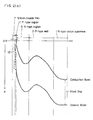
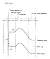
- FIG. 2 (a) shows a potential profile along line A-A in FIG. 1.
- an interface trap level 12 is generated as schematically indicated by X in FIG. 2 (a).
- FIG 2 (b) shows a potential profile along line A-A in FIG. 6.
- the potential profile continues flatly from the N-type region 5 to the interface with the silicon dioxide film 7 as shown by reference numeral 13 in FIG. 2 (b).
- the electrons generated from the interface trap level flow into the N-type region 5, which causes the dark current.
- FIG. 1 shows a potential profile along line A-A in FIG. 1.
- the P-type region 11 is buried in the surface portion of the N-type region 5, and this P-type region 11 is connected to the grounding potential. Accordingy, the potential profile is fixed at 0V in the P-type region 11 as shown in FIG. 2 (a). As a result, the electrons generated at the interface trap level disappears by re-combining with holes through the P-type region 11. Therefore, the electrons generated at the interface trap level do not flow into the N-type region 5, and hence the dark current is suppressed notably.
- the affects of the interface trap level in the region indicated by l1 in FIG. 1 may be also suppressed.
- l1 is set at about 0.5 ⁇ m, that is, about the depth of function of the P-type region 11, the P-type impurity is diffused nearly to the lower part of the polycrystalline silicon electrode 8, which may affect the potential profile in the reading action of the signal electric charge.
- the image lag due to imperfect pickup of the signal electric change may be likely to occur. Therefore, the value of l1 must be determined considering the shape of photo diode and impurity profile of N-type region 5 etc.
- setting l1 at 0.8 ⁇ m the P-type region 11 was formed in about 80 percent of the surface area of the N-type region 5. At this time, the dark current was decreased to about 25% of the conventional level.
- the impurity concentration of the P-type region 11 is 2 x 10¹⁸/cm3. According to the experiment by the present inventors, when the impurity concentration of P-type region was in the order of 1017, the stability was poor, and in the order of 1018 or more, depletion of the interface in the ordinary operation could be prevented, and the dark current could be stably suppressed.
- the structure of the reading gate parts of CCD that is, the N-type region 6, polycrystalline silicon electrode 8 and others may be same as in the conventional structure. Therefore, the characteristics relating to the functions of reading out signals are not changed at all. Therefore, it is not required to modify the external circuits connected to the CCD solid state image sensor.
- FIG. 3 (a) to (d) relate to a second embodiment of the invention, sequentially showing sectional views of manufacturing steps of a solid state image sensor capable of controlling the position of the P-type region 11 accurately with respect to the polycrystalline silicon electrode 8, and
- FIG. 4 is a sectional view showing its completion state.
- FIG. 3 and FIG. 4, same as FIG. 1, show only the unit cell portion of the interline transfer type CCD solid state image sensor using PN junction photo diode as photo detector, and the same parts as in FIG. 1 substantially are identified with same reference numerals.
- a polycrystalline silicon electrode 8 is formed on a silicon dioxide film 7. Thereafter, the polycrystalline silicon electrode 8 is oxidized, and the silicon dioxide film 7 of about 2500 ⁇ in thickness is formed on the surface and side face of the polycrystalline silicon electrode 8 [FIG. 3 (b)].
- boron ions (B+) are injected from the surface of the silicon dioxide film 7 toward the substrate surface.
- boron ions are injected through the silicon dioxide film 7, and at this time the silicon dioxide film at the side face of the polycrystalline silicon electrode 8 is thick, and therefore the polycrystalline silicon electrode 8 and the silicon dioxide film 7 at its side face work as masks when injecting ions. Accordingly, boron irons are injected into the region remote from the edge of the polycrystalline silicon electrode 8. The gap between the edge of the polycrystalline silicon electrode 8 and the boron injection region is determined by the film thickness of the silicon dioxide film 7 at the side face of the polycrystalline silicon electrode 8 grown in FIG. 3 (b).
- the impurities of boron ions are diffused toward the polycrystalline silicon electrode 8, thereby forming a P-type region 11 in a shape partly overlapping with the polycrystalline silicon electrode 8 [FIG. 3 (d)].
- the overlapping width of polycrystalline silicon electrode 8 and N-type region 5 is set at 1.0 ⁇ m, longer than the junction depth 0.5 ⁇ m of the P-type region 11 and the P-type region 11 is diffused up to beneath the polycrystalline silicon electrode 8, the boron concentration profile beneath the polycrystalline silicon electrode 8 can be accurately controlled by optimizing the film thickness of the silicon dioxide film 7 at the side face of thepolycrystalline silicon electrode 8 in FIG. 3 (c) and the thermal diffusion conditions in FIG. 3 (d), and as a result the dark current characteristic and image lag characteristic can be improved at the same time.
- the feature of the second embodiment of the invention disclosed in FIGS. 3, 4 is that the position or the area of the P-type region 11 is accurately controlled by self-alignment on the basic of the end portion of the polycrystalline silicon electrode 8. That is, in FIG. 3 (b), the film thickness of the silicon dioxide film 7 at the side face of the polycrystalline silicon electrode 8 can be accurately controlled. Besides, in FIG. 3 (c), since boron ions are injected by using the polycrystalline silicon electrode 8 and silicon dioxide film 7 as masks, the shape of the P-type region 11 can be accurately controlled. Moreover, when the heat treatment condition in FIG. 3 (d) is optimized, the boron concentration profile beneath the polycrystalline silicon electrode 8 may be also controlled accurately.
- the aluminum film 9 for cutting off light is formed within the top area of the polycrystalline silicon electrode 8 or in a size slightly projecting from the end portion of the polycrystalline silicon electrode 8. Accordingly, the light obliquely entering the photo diode (PD) from upper right to the lower left corner of the drawing may pass near the end portion of the polycrystalline silicon electrode 8 to directly enter the CCD part.
- the CCD directly receives an oblique incident light in this way, the signal electric charges due to the oblique incident light may be added to the original transfer electric charges during CCD reading period, and it may become a kind of false signal to make the image unclear, which is known as smear phenomenon.
- FIG. 5 shows a third embodiment capable of solving such problem.
- FIG. 5 also shows, same as the first and second embodiments, only the unit cell portion of the interline transfer type CCD solid state image sensor using PN junction photo diode as the photo detector.
- the part substantially same in function as those in FIGS. 1, 3 are identified with same reference numerals, and the detailed explanation is omitted.
- an aluminum film 14 for cutting off light is formed on the surface of a silicon dioxide film 7, an aluminum film 14 for cutting off light is formed in the portion excluding the region of the photo diode (PD).
- the end portion of the aluminum film 14 is formed so as to over the surface of the silicon dioxide film 7 at both sides of the polycrystalline silicon electrode 8. In this way, as shown in FIG.
- the aluminum film 14 is extended to the photo diode (PD) by the total dimension of the film thickness l3 of silicon dioxide film 7 and the film thickness l4 of aluminum film 14.
- the oblique light entering the CCD part may be securely blocked at the end portion of the aluminum film 14, so that generation of smear may be notably suppressed.
- P-type well 2 is used as the substrate.
- the epitaxilaly grown P-type well 2 is used as the substrate.
- the excess electric charge is designed to overflow into the N-type silicon substrate 1, but a similar effect is obtained in a method of sweeping out the excess electric charge into the drain formed in the substrate surface portion.
- the N-type silicon substrate 1 is used, but it may be also possible, needless to say, to use the P-type silicon substrate.
Landscapes
- Solid State Image Pick-Up Elements (AREA)
- Transforming Light Signals Into Electric Signals (AREA)
- Picture Signal Circuits (AREA)
- Light Receiving Elements (AREA)
Applications Claiming Priority (6)
| Application Number | Priority Date | Filing Date | Title |
|---|---|---|---|
| JP23766488 | 1988-09-22 | ||
| JP237666/88 | 1988-09-22 | ||
| JP23766588 | 1988-09-22 | ||
| JP23766688 | 1988-09-22 | ||
| JP237665/88 | 1988-09-22 | ||
| JP237664/88 | 1988-09-22 |
Publications (2)
| Publication Number | Publication Date |
|---|---|
| EP0360595A2 true EP0360595A2 (de) | 1990-03-28 |
| EP0360595A3 EP0360595A3 (de) | 1990-05-09 |
Family
ID=27332493
Family Applications (1)
| Application Number | Title | Priority Date | Filing Date |
|---|---|---|---|
| EP89309584A Withdrawn EP0360595A3 (de) | 1988-09-22 | 1989-09-20 | Festkörperbildsensor |
Country Status (3)
| Country | Link |
|---|---|
| US (1) | US5043783A (de) |
| EP (1) | EP0360595A3 (de) |
| JP (1) | JP2781425B2 (de) |
Cited By (7)
| Publication number | Priority date | Publication date | Assignee | Title |
|---|---|---|---|---|
| EP0457192A1 (de) * | 1990-05-14 | 1991-11-21 | Nec Corporation | Festkörperbildaufnahmevorrichtung zur Beschleunigung elektrischer Ladungen von der photoelektrischen Konvertierungsregion mittels elektrischem Feld zum Transferregister |
| EP0463455A3 (en) * | 1990-06-25 | 1992-02-12 | Matsushita Electronics Corporation | Solid-state image pickup device, process for its manufacture, and method of driving the device |
| EP0435309B1 (de) * | 1989-12-28 | 1997-03-12 | Kabushiki Kaisha Toshiba | Festkörper-Bildaufnahmevorrichtung und deren Herstellungsmethode |
| NL1003930C2 (nl) * | 1995-09-01 | 1998-10-14 | Sony Corp | Vaste stof beeldopname-element. |
| GB2324651A (en) * | 1997-04-25 | 1998-10-28 | Vlsi Vision Ltd | Solid state image sensor |
| WO2005013370A1 (en) * | 2003-07-30 | 2005-02-10 | Micron Technology, Inc. | Angled pinned photodiode for high quantum efficiency and method of formation |
| US7122408B2 (en) * | 2003-06-16 | 2006-10-17 | Micron Technology, Inc. | Photodiode with ultra-shallow junction for high quantum efficiency CMOS image sensor and method of formation |
Families Citing this family (18)
| Publication number | Priority date | Publication date | Assignee | Title |
|---|---|---|---|---|
| JP2595138B2 (ja) * | 1990-06-14 | 1997-03-26 | 三菱電機株式会社 | 固体撮像素子及びその製造方法 |
| JP3125303B2 (ja) * | 1990-11-26 | 2001-01-15 | 日本電気株式会社 | 固体撮像素子 |
| JPH04355964A (ja) * | 1990-12-21 | 1992-12-09 | Mitsubishi Electric Corp | 固体撮像装置及びその製造方法 |
| US5238864A (en) * | 1990-12-21 | 1993-08-24 | Mitsubishi Denki Kabushiki Kaisha | Method of making solid-state imaging device |
| JP2970158B2 (ja) * | 1991-12-20 | 1999-11-02 | 日本電気株式会社 | 固体撮像装置の製造方法 |
| JPH07153988A (ja) * | 1993-12-01 | 1995-06-16 | Nikon Corp | 「増幅型」光電変換装置及びその駆動方法 |
| US5563429A (en) * | 1994-06-14 | 1996-10-08 | Nikon Corp. | Solid state imaging device |
| JP3697769B2 (ja) * | 1995-02-24 | 2005-09-21 | 株式会社ニコン | 光電変換素子及び光電変換装置 |
| JP2848268B2 (ja) * | 1995-04-20 | 1999-01-20 | 日本電気株式会社 | 固体撮像装置およびその製造方法 |
| JP3412390B2 (ja) * | 1996-03-18 | 2003-06-03 | 株式会社ニコン | 光電変換装置 |
| TW393777B (en) | 1997-09-02 | 2000-06-11 | Nikon Corp | Photoelectric conversion devices and photoelectric conversion apparatus employing the same |
| US6677628B2 (en) * | 1998-09-17 | 2004-01-13 | Micron Technology, Inc. | Pinned floating photoreceptor with active pixel sensor |
| JP3688980B2 (ja) * | 2000-06-28 | 2005-08-31 | 株式会社東芝 | Mos型固体撮像装置及びその製造方法 |
| JP4442157B2 (ja) | 2003-08-20 | 2010-03-31 | ソニー株式会社 | 光電変換装置及び固体撮像装置 |
| JP4613305B2 (ja) * | 2004-10-19 | 2011-01-19 | 国立大学法人静岡大学 | 埋め込みフォトダイオード構造による撮像装置 |
| US8446508B2 (en) * | 2005-07-27 | 2013-05-21 | Sony Corporation | Solid state imaging device with optimized locations of internal electrical components |
| JP2007208052A (ja) * | 2006-02-02 | 2007-08-16 | Fujifilm Corp | 固体撮像素子 |
| JP2012124515A (ja) * | 2012-02-08 | 2012-06-28 | Canon Inc | 固体撮像装置およびその製造方法 |
Family Cites Families (14)
| Publication number | Priority date | Publication date | Assignee | Title |
|---|---|---|---|---|
| JPS5946155B2 (ja) * | 1976-07-02 | 1984-11-10 | ソニー株式会社 | 固体撮像装置 |
| US4484210A (en) * | 1980-09-05 | 1984-11-20 | Nippon Electric Co., Ltd. | Solid-state imaging device having a reduced image lag |
| US4527182A (en) * | 1980-09-19 | 1985-07-02 | Nippon Electric Co., Ltd. | Semiconductor photoelectric converter making excessive charges flow vertically |
| JPS57194570A (en) * | 1981-05-27 | 1982-11-30 | Toshiba Corp | Solid state image pick-up device and manufacture thereof |
| JPS58171A (ja) * | 1981-06-25 | 1983-01-05 | Toshiba Corp | 固体撮像素子 |
| JPS59130466A (ja) * | 1983-01-17 | 1984-07-27 | Nec Corp | 固体撮像素子 |
| JPS6114749A (ja) * | 1984-06-29 | 1986-01-22 | Fujitsu Ltd | 半導体装置 |
| JPH0773347B2 (ja) * | 1985-10-18 | 1995-08-02 | 日本電気株式会社 | 固体撮像装置の駆動方法 |
| JPS62124771A (ja) * | 1985-11-25 | 1987-06-06 | Sharp Corp | 固体撮像装置 |
| JPH01500471A (ja) * | 1986-07-24 | 1989-02-16 | イーストマン・コダック・カンパニー | ホトダイオードを用いたイメージセンサのための電子シャッタ |
| JP2583897B2 (ja) * | 1987-07-22 | 1997-02-19 | 松下電子工業株式会社 | 固体撮像装置およびその駆動方法 |
| JPH01135184A (ja) * | 1987-11-19 | 1989-05-26 | Nec Corp | 固体撮像素子 |
| JPH01147862A (ja) * | 1987-12-04 | 1989-06-09 | Hitachi Ltd | 固体撮像素子 |
| JPH0230183A (ja) * | 1988-07-19 | 1990-01-31 | Nec Corp | 固体撮像素子 |
-
1989
- 1989-09-20 EP EP89309584A patent/EP0360595A3/de not_active Withdrawn
- 1989-09-20 JP JP1243845A patent/JP2781425B2/ja not_active Expired - Fee Related
- 1989-09-22 US US07/411,094 patent/US5043783A/en not_active Expired - Fee Related
Cited By (14)
| Publication number | Priority date | Publication date | Assignee | Title |
|---|---|---|---|---|
| EP0435309B1 (de) * | 1989-12-28 | 1997-03-12 | Kabushiki Kaisha Toshiba | Festkörper-Bildaufnahmevorrichtung und deren Herstellungsmethode |
| EP0457192A1 (de) * | 1990-05-14 | 1991-11-21 | Nec Corporation | Festkörperbildaufnahmevorrichtung zur Beschleunigung elektrischer Ladungen von der photoelektrischen Konvertierungsregion mittels elektrischem Feld zum Transferregister |
| EP0463455A3 (en) * | 1990-06-25 | 1992-02-12 | Matsushita Electronics Corporation | Solid-state image pickup device, process for its manufacture, and method of driving the device |
| US5262661A (en) * | 1990-06-25 | 1993-11-16 | Matsushita Electric Industrial Co., Ltd. | Solid-state image pickup device, having increased charge storage and improved electronic shutter operation |
| US5324669A (en) * | 1990-06-25 | 1994-06-28 | Matsushita Electronics Corporation | Process for manufacturing a solid state image pickup device having increased charge storage and improved electronic shutter operation |
| NL1003930C2 (nl) * | 1995-09-01 | 1998-10-14 | Sony Corp | Vaste stof beeldopname-element. |
| GB2324651A (en) * | 1997-04-25 | 1998-10-28 | Vlsi Vision Ltd | Solid state image sensor |
| GB2324651B (en) * | 1997-04-25 | 1999-09-01 | Vlsi Vision Ltd | Improved solid state image sensor |
| US7122408B2 (en) * | 2003-06-16 | 2006-10-17 | Micron Technology, Inc. | Photodiode with ultra-shallow junction for high quantum efficiency CMOS image sensor and method of formation |
| US7226803B2 (en) | 2003-06-16 | 2007-06-05 | Micron Technology, Inc. | Photodiode with ultra-shallow junction for high quantum efficiency CMOS image sensor and method of formation |
| US7573113B2 (en) | 2003-06-16 | 2009-08-11 | Micron Technology, Inc. | Photodiode with ultra-shallow junction for high quantum efficiency CMOS image sensor and method of formation |
| US7662658B2 (en) | 2003-06-16 | 2010-02-16 | Micron Technology, Inc. | Photodiode with ultra-shallow junction for high quantum efficiency CMOS image sensor and method of formation |
| WO2005013370A1 (en) * | 2003-07-30 | 2005-02-10 | Micron Technology, Inc. | Angled pinned photodiode for high quantum efficiency and method of formation |
| US6900484B2 (en) | 2003-07-30 | 2005-05-31 | Micron Technology, Inc. | Angled pinned photodiode for high quantum efficiency |
Also Published As
| Publication number | Publication date |
|---|---|
| EP0360595A3 (de) | 1990-05-09 |
| US5043783A (en) | 1991-08-27 |
| JPH02168670A (ja) | 1990-06-28 |
| JP2781425B2 (ja) | 1998-07-30 |
Similar Documents
| Publication | Publication Date | Title |
|---|---|---|
| EP0360595A2 (de) | Festkörperbildsensor | |
| EP1034570B1 (de) | Schutzring zur verminderung des dunkelstroms | |
| EP1130638B1 (de) | Verfahren und Struktur zur Verringerung des Leckstroms der lichtempfindlichen Fläche einer PhotoDiode | |
| US5514887A (en) | Solid state image sensor having a high photoelectric conversion efficiency | |
| KR100262774B1 (ko) | 상부 버스 가상 위상 프레임 행간 전송 ccd 영상 감지기 | |
| US7235831B2 (en) | Light-receiving element and photoelectric conversion device | |
| US6169318B1 (en) | CMOS imager with improved sensitivity | |
| KR20060126377A (ko) | 비대칭 전송 게이트 채널 도핑을 갖는 픽셀 | |
| KR980012585A (ko) | 수직형 전달게이트를 가지는 전하결합형 고체촬상소자 및 그 제조방법 | |
| US7015522B2 (en) | Solid-state image sensor | |
| US6501109B1 (en) | Active CMOS pixel with exponential output based on the GIDL mechanism | |
| US5118631A (en) | Self-aligned antiblooming structure for charge-coupled devices and method of fabrication thereof | |
| KR960001951B1 (ko) | 고체촬상장치의 제조방법 | |
| KR100324192B1 (ko) | 고체 촬상 소자 구동 방법 | |
| KR100813800B1 (ko) | 암전류 특성과 전하저장능력을 향상시킨 이미지센서 및 그제조방법 | |
| JPH0789581B2 (ja) | 固体撮像装置およびその製造方法 | |
| KR100262006B1 (ko) | 고체촬상소자 및 그 제조방법 | |
| JPH0697416A (ja) | 固体撮像装置及びその製造方法 | |
| KR0172853B1 (ko) | 씨씨디 고체촬상소자 | |
| KR890004985B1 (ko) | 폴리실리콘을 이용한 차단층을 갖는 고체영상소자 | |
| JPH10116975A (ja) | 固体撮像装置及び固体撮像装置のオーバーフローバリア形成方法 | |
| JPS60105382A (ja) | 固体撮像素子 | |
| HK1029439B (en) | Dark current reducing guard ring | |
| JPH03285355A (ja) | 固体撮像素子およびその製造方法 | |
| JPS61229356A (ja) | 固体撮像装置 |
Legal Events
| Date | Code | Title | Description |
|---|---|---|---|
| PUAI | Public reference made under article 153(3) epc to a published international application that has entered the european phase |
Free format text: ORIGINAL CODE: 0009012 |
|
| PUAL | Search report despatched |
Free format text: ORIGINAL CODE: 0009013 |
|
| 17P | Request for examination filed |
Effective date: 19891212 |
|
| AK | Designated contracting states |
Kind code of ref document: A2 Designated state(s): DE FR GB NL |
|
| AK | Designated contracting states |
Kind code of ref document: A3 Designated state(s): DE FR GB NL |
|
| 17Q | First examination report despatched |
Effective date: 19930705 |
|
| STAA | Information on the status of an ep patent application or granted ep patent |
Free format text: STATUS: THE APPLICATION IS DEEMED TO BE WITHDRAWN |
|
| 18D | Application deemed to be withdrawn |
Effective date: 19950912 |