EP0400963A2 - Hochfrequenz-Elementarresonanzvorrichtung mit kompensierbaren Frequenz-Temperaturcharakteristiken - Google Patents
Hochfrequenz-Elementarresonanzvorrichtung mit kompensierbaren Frequenz-Temperaturcharakteristiken Download PDFInfo
- Publication number
- EP0400963A2 EP0400963A2 EP90305826A EP90305826A EP0400963A2 EP 0400963 A2 EP0400963 A2 EP 0400963A2 EP 90305826 A EP90305826 A EP 90305826A EP 90305826 A EP90305826 A EP 90305826A EP 0400963 A2 EP0400963 A2 EP 0400963A2
- Authority
- EP
- European Patent Office
- Prior art keywords
- temperature
- general formula
- ceramic
- elemental device
- disorder
- Prior art date
- Legal status (The legal status is an assumption and is not a legal conclusion. Google has not performed a legal analysis and makes no representation as to the accuracy of the status listed.)
- Granted
Links
Images


Classifications
-
- H—ELECTRICITY
- H01—ELECTRIC ELEMENTS
- H01P—WAVEGUIDES; RESONATORS, LINES, OR OTHER DEVICES OF THE WAVEGUIDE TYPE
- H01P11/00—Apparatus or processes specially adapted for manufacturing waveguides or resonators, lines, or other devices of the waveguide type
- H01P11/008—Manufacturing resonators
-
- H—ELECTRICITY
- H01—ELECTRIC ELEMENTS
- H01P—WAVEGUIDES; RESONATORS, LINES, OR OTHER DEVICES OF THE WAVEGUIDE TYPE
- H01P7/00—Resonators of the waveguide type
- H01P7/10—Dielectric resonators
Definitions
- the present invention relates to a resonant frequency-temperature characteristics compensable elemental device, in particular to a device utilizing resonance phenomena of a dielectric ceramic such as resonator systems and oscillator systems of which the resonant frequency temperature coefficient can be compensated by heat-treating the dielectric ceramic used therein.
- Cavity resonators, ring resonators, dielectric resonators or the like are used in oscillating systems and filters for communication using high-frequencies such as microwave and milimeter wave.
- the dielectric resonators are used extensively by virtue of the advantages that they have good temperature stability of resonant frequencies and are suitable for miniaturization of devices.
- High frequency circuit elemental devices comprising a dielectric resonator mounted in a casing include, for example, resonator systems, oscillators for stabilizing high frequencies and filters. It is required for such devices to have good temperature stability of resonant frequencies (or oscillating frequencies) as a whole.
- local oscillators one of said oscillators, are assembled by mounting a dielectric resonator, FETs, strip lines, etc. in a casing. In the case of this oscillator, it is required that the influences on the temperature characteristics of the dielectric resonator by the other parts such as FETs and the casing are compensated so that the device may have a temperature coefficient of 0 or so as a whole.
- the temperature coefficient ( ⁇ f ) of resonant frequency of a dielectric ceramic is fixed based on the composition of the dielectric ceramic. Accordingly, in order to enable the assembled device to have a desired temperature characteristics as a whole, it has been so far necessary to produce a great number of dielectric ceramics having diversity of ⁇ f in advance, to choose a ceramic with a suitable ⁇ f for assembly so that the influences by the other parts may be compensated.
- the above method of assembly is, however, disadvantageous in that a great number of dielectric ceramics having diversity of ⁇ f must be produced in advance by changing the composition of individual ceramics. This is extremely troublesome.
- the ceramic produced by this process cannot undergo order-disorder transformation in crystal structure unlike the dielectric ceramic used in the present invention described later. Hence it is impossible to allow the temperature coefficient of the resonant frequencies to be changed by heat-treatment.
- an object of the present invention to provide a high frequency circuit elemental device the temperature characteristics of the resonant or oscillating frequency of which can be compensated by merely heat-treating the dielectric ceramic used therein without changing the composition of the ceramic even after assembly of the device.
- the present invention provides a high frequency circuit elemental device comprising a casing and a dielectric ceramic mounted in said casing, said dielectric ceramic being capable of undergoing order-disorder structural transformation, whereby the temperature coefficient of the resonant frequency can be compensated by heat-treatment.
- the temperature characteristics of the resonant frequency of the dielectric ceramic mounted in the device is controllable by heat-treatment. Hence, the temperature characteristics of the resonance frequency of the whole assembled device can be markedly readily compensated.
- the high frequency circuit elemental device includes, for example, resonator systems, oscillating systems and filters and the like comprised of a casing and a dielectric ceramic mounted therein.
- order-disorder structural transformation means (1) reversible transformations in structure which take place by heat-treatment because the substance has so-called a phase transition temperature, and (2) irreversible transformations in structure which take place when an disordered phase formed in non-equilibrium is converted into an ordered phase by heat-treatment.
- the dielectric ceramics used in two preferred embodiments described below of the present invention have a perovskite-type complex crystal structure which can undergo reversible order-disorder structural transformation.
- Heat-treatment at a temperature below its transition temperature results in structural transformation of from a disordered state to an ordered state; while on the other hand, heat-treatment at a temperature above the transition temperature results in the reverse structural transformation.
- ⁇ f is changed.
- the terminology "disordered crystal structure” means a perovskite type complex crystal structure of which degree of disorder defined by the equation below is 0.4 or less.
- order crystal structure means a structure having a degree of disorder of more than 0.4.
- the (100), (110) and (102) are plane indices of the hexagonal system applied to an X-ray diffraction pattern; and the diffraction intensity A is that of a ceramic to be measured and the diffraction intensity B is that of a ceramic with a completely ordered structure.
- the dielectric ceramic a dielectric ceramic essentially consisting of a compound having an order-disorder structurally transformable perovskite-type complex crystal structure and having the composition represented by the general formula (I): Ba x A y B 1-x-y F z O w (I) wherein A represents at least one element selected from the group consisting of Mg, Zn, Ni and Co; B is at least one element selected from the group consisting of Ta and Nb; x, y and z are a number of 0.48 ⁇ x ⁇ 0.52, 0.15 ⁇ y ⁇ 0.19, and 0.00025 ⁇ z ⁇ 0.05, respectively; and w is a number that neutralizes the total electric charge of cations of Ba, A and B and anions of F so that the ceramic may be neutral electrically as a whole, and produced by a process comprising the steps of: calcining a mixture of compounds selected from the group consisting of oxides, fluorides, oxyfluorides and compounds of the metal
- x is a number of from 0.48 to 0.52, preferably from 0.49 to 0.51
- y is a number of from 0.15 to 0.19, preferably from 0.16 to 0.18
- z is a number of from 0.00025 to 0.05, preferably from 0.0005 to 0.01. If x, y and/or z is outside the range specified above, desired dielectric properties cannot be attained.
- the symbol w represents a number such that the cations of Ba, A and B, and the anions of F constituting the ceramic are neutralized electrically. The value of w is automatically fixed based on the values of x, y and z, as well as, if the A contains Co, the valence of Co, and is normally in a range of from 1.49 to 1.51.
- raw materials of constituent metals are weighed, and mixed in desired amounts according to an intended composition of the general formula (I), and dried, followed by the calcination described above.
- the raw material compounds which may be used as sources of the constituent metals include, for example, oxides, fluorides and oxyfluorides as well as all sorts of compounds which can be converted into oxides, fluorides or oxyfluorides under the conditions of the calcining or firing step, and specifically include, for example, hydroxides and carbonates.
- Examples of such compounds include barium carbonate, magnesium oxide, zinc oxice, nickel oxide, cobalt oxide, tantalum oxides such as tantalum pentaoxide, and niobium oxides such as niobium pentoxide, fluorides such as barium fluoride, magnesium fluoride, zinc fluoride, nickel fluoride, cobalt fluoride, and tantalum fluoride, oxyfluorides such as TaOF3, TaO2F and NbO2F, double fluorides such as Ba2MgF6, Ba2NiF6, BaNiF4, Ba2CoF6, and BaCoF4.
- fluorides and oxyfluorides are sources of metal components as well as fluorine.
- fluorine sources which may be used include potassium fluoride, sodium fluoride and lithium fluoride.
- the amounts of the raw materials are preferably set with consideration of easiness or hardness in evaporation of individual components so that a dielectric ceramic with an intended composition may be prepared.
- the calcination is normally carried out at 900 to 1,400°C, preferably at 1,000 to 1,200°C.
- the calcined product obtained may be normally ground and graded if required, and thereafter is molded, and subjected to firing. Firing is carried out by heating the molded product at a rate of from 100 to 1,600°C/min., preferably from 300 to 1,600°C/min, up to a temperature of not less than the order-disorder transition temperature of said intended compound of the general formula (I), specifically from 1,450 to 1,700°C, and maintaining the molded product at the temperature for at least 1 minute, preferably from about 2 minutes to 4 hours. If the heat-treating temperature is below 1,450°C, the sintered density of a ceramic obtained may be not increased sufficiently; if it is above 1,700°C, the structure of the ceramic may be liable to get brittle. In general, heat-treating time after the rapid heating may be shortened with increase in the temperature of heat-treatment.
- the fluorine used as a ceramic component in this embodiment promotes sintering to facilitate the formation of a dense ceramic, and also advantageously serves to enhance relative dielectric constant and unloaded Q.
- the calcination step and the firing step described above may be carried out in any of oxidizing atmosphere such as oxygen and air, and inert atmosphere such as nitrogen. Normally air can be used satisfactorily.
- the dielectric ceramic a dielectric ceramic essentially consisting of a compound having an order-disorder structurally transformable perovskite-type complex crystal structure and having a composition represented by the general formula (II): Ba x A y B 1-x-y O w (II) wherein A represents at least one element selected from the group consisting of Mg, Zn, Ni and Co; B is at least one element selected from the group consisting of Ta and Nb; x and y are a number of 0.48 ⁇ x ⁇ 0.52, and 0.15 ⁇ y ⁇ 0.19, respectively; and w is a number that neutralizes the total electric charge of cations Ba, A and B so that the ceramic may be neutral electrically as a whole, and produced by a process comprising the steps of: calcining a mixture of compounds selected from the group consisting of oxides and compounds of the metals constituting said compound of the general formula (II) which are converted into oxides under the heating conditions of this calc
- the compound constituting dielectric ceramic used in the second embodiment needs to essentially have the composition represented by the general formula (II).
- this requirement does not exclude incorporation of fluorine in such an amount that z in the general formula (I) has a number of z ⁇ 0.00025.
- Both of the dielectrics used in the devices of the first and second embodiments have a disordered crystal structure at the stage of completion of the heat-treatment, but the crystal structures can be transformed reversibly at their oder-disorder transition temperature.
- the order-disorder transition temperature exists generally in a range of from about 1,400 to about 1,500°C.
- the order-disorder transition temperature of a specific ceramic can be determined readily by experiments using X-ray diffractometry, thermal analysis, etc.
- Heat-treatment of the above mentioned dielectric ceramics used in the embodiments in the vicinity of the below its order-disorder transition temperature causes structural transformation from the disordered state to an ordered state.
- Heating the ceramics thus transformed at a temperature above the order-disorder transition temperature causes structural transformation from the ordered state to a disordered state.
- the time for heat-treatment may be about 10 minutes or longer, normally in the range of from 10 to 50 hours.
- the degree of order of the crystal structure is attended by change in ⁇ f . That is, the structural transformation from the disordered state to the ordered state decreases ⁇ f , and the structural transformation from ordered state to the disordered state increases ⁇ f .
- the ⁇ f also changes depending on the length of heat-treatment; hence, regulating the length of heat-treating time makes it possible to control ⁇ f .
- dielectric ceramics of which ⁇ f can be controlled by irreversibly converting a disordered phase formed in non-equilibrium into an ordered phase include the dielectric ceramic of Ba(Mg 1/3 , Ta 2/3 )O3 containing a disordered phase in non-equilibrium.
- the ordered phase of the ceramic of Ba(Mg 1/3 , Ta 2/3 )O3 is stable at firing step or the like because this ceramic has no phase transition temperature or because its phase transition temperature is very high.
- said ceramic containing the disordered phase in non-equilibrium can be prepared as a semi-stable phase or a precursor of the ordered phase.
- the ⁇ f of the ceramic of Ba(Mg 1/3 , Ta 2/3 )O3 containing the disordered phase can be changed by heat-treatment at about 1,300 to 1,700°C.
- dielectric ceramics of which ⁇ f can be controlled by irreversibly converting a disordered phase formed in non-equilibrium into an ordered phase include the dielectric ceramics of Ba(Zn 1/3 , Ta 2/3 )O3, Sr(Mg 1/3 , Ta 2/3 )O3, and Sr(Zn 1/3 , Ta 2/3 )O3.
- the device of the present invention comprises a casing and a dielectric ceramic mounted therein, and optionally further comprises FETs, strip lines, etc.
- the device In order for the device to have a desired temperature stability of resonant frequency (or oscillating frequency) as a whole, first, the device is assembled by mounting the dielectric ceramic and all the other parts in the casing, and then the temperature characteristics of resonant frequency of the assembly is measured. If there is a deviation between the designed temperature characteristics and the measured temperature characteristics, said dielectric ceramic is once detached and then is subjected to heat-treatment at a temperature in the vicinity of the order-disorder transition temperature. Thereafter, the ceramic is fitted in the casing again, followed by measurement of the temperature characteristics.
- a dielectric ceramic in the shape of a disc having a diameter of 5.77 mm and a length of 2.90 mm composed of a perovskite-type complex compound having the composition of the formula: Ba(Zn 0.8 Ni 0.1 Co 0.1 ) 1/3 (Ta 0.6 Nb 0.4 ) 2/3 which is an order-disorder structurally transformable compound, was produced as follows.
- barium carbonate, zinc oxide, nickel oxide, cobalt oxide, tantalum oxide and nibium oxide, each with a purity of 99.9%, were weighed so as to give the composition represented by the above formula, and were mixed in pure water with a ball mill for 16 hours. The mixture was dried, and then calcined at 1,000°C for 2 hours, followed by grinding. The calcined product was molded into a molded product with a diameter of 8 mm and a length of 4 mm, which was then heated at a rate of 600°C/min. up to 1,600°C, and was maintained at 1,600°C for 5 minutes to produce a dielectric ceramic. This ceramic was then worked so as to give a desired disc with dimentions above.
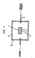
- the dielectric ceramic 1 was fixed in the center of a copper-coated cavity 2 made of brass using a quartz tube 3 as a support, thereby a resonator system 5 was produced.
- the resonator system was swept from its side in the microwave zone by allowing semi-rigid cable 4 to short-circuit at one end as a probe.
- the resonance point in TE018 mode was observed at about 9.2 GHz.
- the resonator system 5 was placed in a thermostatic chamber.
- the drift of the resonance in TE018 mode by change in temperature was measured over a range from 0°C to 60°C; thus the results shown in fig. 2 were obtained.
- the temperature coefficient at 20°C was found to be about 2.2 ppm/°C.
- the dielectric ceramic was heat-treated at 1,400°C which is below the order-disorder transition temperature for 50 hours.
- the drift by change in temperature was measured again in the same manner as above, and the results shown in Fig. 3 were thereby obtained. This temperature coefficient became - 0.8 ppm/°C.
- the temperature characteristics exhibit a drift of 500 kHz or less over the range from 0°C to 60°C, which indicates that the resonator system obtained has markedly high temperature stability.
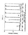
- the ceramic used in the above resonator system before the above heat-treatment and the same after the above heat-treatment were separately ground, and then subjected to X-ray diffractometry for the purpose of measuring intensities of super lattice lines due to ordered crystal structures.
- the ceramic before the heat-treatment gave the X-ray diffraction pattern shown in Fig. 4, which is similar to the pattern of the disordered perovskite-type complex crystal structure represented by Ba(Zn 1/3 Nb 2/3 )3; therefore the ceramic was found to have a disordered crystal structure.
- the ceramic after the heat-treatment gave the X-ray diffraction pattern shown in Fig. 5, which is similar to the pattern of the ordered perovskite-type complex crystal structure represented by Ba(Zn 1/3 Ta 2/3 )3; therefore the ceramic was found to have an ordered crystal structure.
- a dielectric ceramic having the composition represented by the formula: Ba(Zn 0.8 Ni 0.1 Co 0.1 ) 1/3 (Ta 0.6 Nb 0.4 ) 2/3 F 0.04 O 2.998 was produced in the same manner as in Example 1, except that BaF2 was used as a fluorine source in addition to the starting materials used in Example 1.
- a resonator system was assembled in the same manner as in Example 1, except that the dielectric ceramic prepared above was used.
- the resonance point in TE018 mode was measured to be about 9.2 GHz.
- Example 2 The temperature characteristics were measured over the range from 0 to 60°C in the same manner as in Example 1. Similar results to those in Example 1 were obtained.
- the temperature coefficient at 20°C was measured to be 2.5 ppm/°C. After heat-treatment at 1,400°C for 25 hours, the temperature coefficient was measured to be - 0.7 ppm/°C.
Landscapes
- Engineering & Computer Science (AREA)
- Manufacturing & Machinery (AREA)
- Inorganic Insulating Materials (AREA)
- Compositions Of Oxide Ceramics (AREA)
- Control Of Motors That Do Not Use Commutators (AREA)
- Ceramic Capacitors (AREA)
- Non-Reversible Transmitting Devices (AREA)
- Control Of High-Frequency Heating Circuits (AREA)
- Pyridine Compounds (AREA)
Applications Claiming Priority (2)
| Application Number | Priority Date | Filing Date | Title |
|---|---|---|---|
| JP1136678A JPH0732323B2 (ja) | 1989-05-30 | 1989-05-30 | 共振周波数の温度係数を調整可能な共振器 |
| JP136678/89 | 1989-05-30 |
Publications (3)
| Publication Number | Publication Date |
|---|---|
| EP0400963A2 true EP0400963A2 (de) | 1990-12-05 |
| EP0400963A3 EP0400963A3 (de) | 1992-03-18 |
| EP0400963B1 EP0400963B1 (de) | 1997-03-12 |
Family
ID=15180918
Family Applications (1)
| Application Number | Title | Priority Date | Filing Date |
|---|---|---|---|
| EP90305826A Expired - Lifetime EP0400963B1 (de) | 1989-05-30 | 1990-05-29 | Hochfrequenz-Elementarresonanzvorrichtung mit kompensierbaren Frequenz-Temperaturcharakteristiken |
Country Status (5)
| Country | Link |
|---|---|
| US (1) | US5087902A (de) |
| EP (1) | EP0400963B1 (de) |
| JP (1) | JPH0732323B2 (de) |
| CA (1) | CA2017722C (de) |
| DE (1) | DE69030137T2 (de) |
Families Citing this family (2)
| Publication number | Priority date | Publication date | Assignee | Title |
|---|---|---|---|---|
| JPH0955606A (ja) * | 1995-08-11 | 1997-02-25 | Fujitsu Ltd | 無線装置用フィルタ装置並びに無線装置用フィルタ装置の誘電体配置用治具並びに治具を用いた無線装置用フィルタ装置の誘電体配置方法 |
| EP3069612A3 (de) | 2009-06-15 | 2016-10-19 | Encore Health, LLC | Dithiolverbindungen, derivate davon und verwendungen davon |
Family Cites Families (16)
| Publication number | Priority date | Publication date | Assignee | Title |
|---|---|---|---|---|
| US4109359A (en) * | 1976-06-07 | 1978-08-29 | The United States Of America As Represented By The Secretary Of The Navy | Method of making ferroelectric crystals having tailored domain patterns |
| JPS52153359A (en) * | 1976-06-14 | 1977-12-20 | Murata Manufacturing Co | Dielectric resonator |
| JPS5948484B2 (ja) * | 1976-09-14 | 1984-11-27 | 松下電器産業株式会社 | 誘電体共振器 |
| US4121941A (en) * | 1977-11-10 | 1978-10-24 | Matsushita Electric Industrial Co., Ltd. | Low microwave loss ceramics and method of manufacturing the same |
| CA1134128A (en) * | 1978-12-04 | 1982-10-26 | Syunichiro Kawashima | Dielectric ceramics |
| JPS5721101A (en) * | 1980-07-14 | 1982-02-03 | Murata Mfg Co Ltd | Electronic device using porcelain dielectric substance resonator |
| JPS58113332A (ja) * | 1981-12-14 | 1983-07-06 | Res Inst Electric Magnetic Alloys | 温度の広範囲にわたり電気抵抗の変化の小さい合金およびその製造方法 |
| JPS61107609A (ja) * | 1984-10-30 | 1986-05-26 | 住友金属鉱山株式会社 | 高周波用誘電体磁器の製造方法 |
| US4563661A (en) * | 1984-12-26 | 1986-01-07 | At&T Bell Laboratories | Dielectric for microwave applications |
| JPH0669904B2 (ja) * | 1985-07-29 | 1994-09-07 | ソニー株式会社 | 誘電体磁器 |
| GB2184432B (en) * | 1985-10-18 | 1989-10-18 | Sumitomo Metal Mining Co | Dielectric ceramic |
| EP0252668B1 (de) * | 1986-02-21 | 1992-01-29 | Sumitomo Metal Mining Company Limited | Dielektrische Keramiken |
| JPS6460905A (en) * | 1987-08-31 | 1989-03-08 | Alps Electric Co Ltd | Dielectric porcelain compound |
| JPH0719485B2 (ja) * | 1987-12-16 | 1995-03-06 | 住友金属鉱山株式会社 | 誘電体磁器及びその製造方法 |
| JPH0625024B2 (ja) * | 1988-11-16 | 1994-04-06 | 住友金属鉱山株式会社 | 誘電体磁器の製造方法 |
| JPH0625025B2 (ja) * | 1989-05-30 | 1994-04-06 | 住友金属鉱山株式会社 | 誘電体磁器の製造方法 |
-
1989
- 1989-05-30 JP JP1136678A patent/JPH0732323B2/ja not_active Expired - Fee Related
-
1990
- 1990-05-29 CA CA002017722A patent/CA2017722C/en not_active Expired - Fee Related
- 1990-05-29 EP EP90305826A patent/EP0400963B1/de not_active Expired - Lifetime
- 1990-05-29 DE DE69030137T patent/DE69030137T2/de not_active Expired - Fee Related
- 1990-05-30 US US07/530,284 patent/US5087902A/en not_active Expired - Lifetime
Also Published As
| Publication number | Publication date |
|---|---|
| EP0400963B1 (de) | 1997-03-12 |
| JPH031702A (ja) | 1991-01-08 |
| JPH0732323B2 (ja) | 1995-04-10 |
| DE69030137T2 (de) | 1997-10-02 |
| CA2017722C (en) | 1994-02-01 |
| EP0400963A3 (de) | 1992-03-18 |
| US5087902A (en) | 1992-02-11 |
| DE69030137D1 (de) | 1997-04-17 |
| CA2017722A1 (en) | 1990-11-30 |
Similar Documents
| Publication | Publication Date | Title |
|---|---|---|
| Dias et al. | Vibrational studies and microwave dielectric properties of A-site-substituted tellurium-based double perovskites | |
| EP0838446B1 (de) | Dielektrisches Material, Verfahren zu dessen Herstellung und dieses Material enthaltende dielektrische Resonatorvorrichtung | |
| US4487842A (en) | Low-loss microwave dielectric material | |
| KR100415757B1 (ko) | 유전체 자기(誘電體磁器)조성물, 유전체 자기의 제조방법 및 유전체 공진기(共振器) | |
| EP0400963B1 (de) | Hochfrequenz-Elementarresonanzvorrichtung mit kompensierbaren Frequenz-Temperaturcharakteristiken | |
| US5039637A (en) | Process for producing a dielectric ceramic | |
| EP0321243A1 (de) | Dielektrische Keramik | |
| US5057466A (en) | Dielectric ceramic material and method of producing same | |
| EP0400962B1 (de) | Dielektrische Keramik und Verfahren zu deren Herstellung | |
| US6703335B2 (en) | Dielectric ceramic composition and method for designing dielectric ceramic composition | |
| JPH0542762B2 (de) | ||
| JP4535589B2 (ja) | 誘電体磁器及びこれを用いた誘電体共振器 | |
| JP2002187771A (ja) | 誘電体磁器およびこれを用いた誘電体共振器 | |
| JP4959043B2 (ja) | 誘電体磁器組成物及びその製造方法並びに誘電体共振器 | |
| JP3330011B2 (ja) | 高周波用誘電体磁器組成物 | |
| JPH09169567A (ja) | 高周波用誘電体磁器組成物 | |
| JP3330024B2 (ja) | 高周波用誘電体磁器組成物 | |
| JPH05109316A (ja) | マイクロ波用誘電体磁器の製造方法 | |
| JPH04303512A (ja) | 誘電体磁器用仮焼物の製造方法 | |
| JPH07215765A (ja) | 誘電体磁器組成物及びその製造方法 | |
| GB2382574A (en) | Dielectric ceramic composition | |
| JPH04331761A (ja) | 誘電体磁器組成物 | |
| JPS6256099B2 (de) | ||
| JPH05225825A (ja) | 高周波用誘電体磁器組成物 | |
| JPH054942B2 (de) |
Legal Events
| Date | Code | Title | Description |
|---|---|---|---|
| PUAI | Public reference made under article 153(3) epc to a published international application that has entered the european phase |
Free format text: ORIGINAL CODE: 0009012 |
|
| AK | Designated contracting states |
Kind code of ref document: A2 Designated state(s): DE FR GB |
|
| 17P | Request for examination filed |
Effective date: 19901214 |
|
| PUAL | Search report despatched |
Free format text: ORIGINAL CODE: 0009013 |
|
| AK | Designated contracting states |
Kind code of ref document: A3 Designated state(s): DE FR GB |
|
| 17Q | First examination report despatched |
Effective date: 19940926 |
|
| GRAG | Despatch of communication of intention to grant |
Free format text: ORIGINAL CODE: EPIDOS AGRA |
|
| GRAH | Despatch of communication of intention to grant a patent |
Free format text: ORIGINAL CODE: EPIDOS IGRA |
|
| GRAH | Despatch of communication of intention to grant a patent |
Free format text: ORIGINAL CODE: EPIDOS IGRA |
|
| GRAA | (expected) grant |
Free format text: ORIGINAL CODE: 0009210 |
|
| AK | Designated contracting states |
Kind code of ref document: B1 Designated state(s): DE FR GB |
|
| REF | Corresponds to: |
Ref document number: 69030137 Country of ref document: DE Date of ref document: 19970417 |
|
| ET | Fr: translation filed | ||
| PLBE | No opposition filed within time limit |
Free format text: ORIGINAL CODE: 0009261 |
|
| STAA | Information on the status of an ep patent application or granted ep patent |
Free format text: STATUS: NO OPPOSITION FILED WITHIN TIME LIMIT |
|
| 26N | No opposition filed | ||
| REG | Reference to a national code |
Ref country code: GB Ref legal event code: IF02 |
|
| PGFP | Annual fee paid to national office [announced via postgrant information from national office to epo] |
Ref country code: FR Payment date: 20050511 Year of fee payment: 16 |
|
| PGFP | Annual fee paid to national office [announced via postgrant information from national office to epo] |
Ref country code: GB Payment date: 20050525 Year of fee payment: 16 |
|
| PGFP | Annual fee paid to national office [announced via postgrant information from national office to epo] |
Ref country code: DE Payment date: 20050526 Year of fee payment: 16 |
|
| PG25 | Lapsed in a contracting state [announced via postgrant information from national office to epo] |
Ref country code: GB Free format text: LAPSE BECAUSE OF NON-PAYMENT OF DUE FEES Effective date: 20060529 |
|
| PG25 | Lapsed in a contracting state [announced via postgrant information from national office to epo] |
Ref country code: DE Free format text: LAPSE BECAUSE OF NON-PAYMENT OF DUE FEES Effective date: 20061201 |
|
| GBPC | Gb: european patent ceased through non-payment of renewal fee |
Effective date: 20060529 |
|
| REG | Reference to a national code |
Ref country code: FR Ref legal event code: ST Effective date: 20070131 |
|
| PG25 | Lapsed in a contracting state [announced via postgrant information from national office to epo] |
Ref country code: FR Free format text: LAPSE BECAUSE OF NON-PAYMENT OF DUE FEES Effective date: 20060531 |