EP0415526A2 - Halbleiteranordnung mit Leiterschichten - Google Patents
Halbleiteranordnung mit Leiterschichten Download PDFInfo
- Publication number
- EP0415526A2 EP0415526A2 EP90307231A EP90307231A EP0415526A2 EP 0415526 A2 EP0415526 A2 EP 0415526A2 EP 90307231 A EP90307231 A EP 90307231A EP 90307231 A EP90307231 A EP 90307231A EP 0415526 A2 EP0415526 A2 EP 0415526A2
- Authority
- EP
- European Patent Office
- Prior art keywords
- layer wiring
- layer
- nth
- insulating film
- wiring
- Prior art date
- Legal status (The legal status is an assumption and is not a legal conclusion. Google has not performed a legal analysis and makes no representation as to the accuracy of the status listed.)
- Withdrawn
Links
Images


Classifications
-
- H—ELECTRICITY
- H10—SEMICONDUCTOR DEVICES; ELECTRIC SOLID-STATE DEVICES NOT OTHERWISE PROVIDED FOR
- H10W—GENERIC PACKAGES, INTERCONNECTIONS, CONNECTORS OR OTHER CONSTRUCTIONAL DETAILS OF DEVICES COVERED BY CLASS H10
- H10W20/00—Interconnections in chips, wafers or substrates
- H10W20/01—Manufacture or treatment
- H10W20/031—Manufacture or treatment of conductive parts of the interconnections
- H10W20/063—Manufacture or treatment of conductive parts of the interconnections by forming conductive members before forming protective insulating material
-
- H—ELECTRICITY
- H10—SEMICONDUCTOR DEVICES; ELECTRIC SOLID-STATE DEVICES NOT OTHERWISE PROVIDED FOR
- H10W—GENERIC PACKAGES, INTERCONNECTIONS, CONNECTORS OR OTHER CONSTRUCTIONAL DETAILS OF DEVICES COVERED BY CLASS H10
- H10W20/00—Interconnections in chips, wafers or substrates
- H10W20/40—Interconnections external to wafers or substrates, e.g. back-end-of-line [BEOL] metallisations or vias connecting to gate electrodes
- H10W20/41—Interconnections external to wafers or substrates, e.g. back-end-of-line [BEOL] metallisations or vias connecting to gate electrodes characterised by their conductive parts
- H10W20/42—Vias, e.g. via plugs
Definitions
- This invention relates to a semiconductor device having a multi-layer wiring structure, used in the field of semiconductor large-scale integrated circuits. It also relates to a process for making the same.
- nth-layer wiring (n is a natural number) is first formed, thereafter an interlaminar insulating film is formed on the nth-layer wiring over the whole surface of a semiconductor device, then the interlaminar insulating film is selectively removed using a mask to make an opening called a through-hole at the part at which the nth wiring and another n+1th-layer wiring are intended to be connected, and then the n+1th-layer wiring is buried in the through-hole to form a joined part.
- a multi-layer wiring structure in which first-layer wiring and second-layer wiring are connected by the formation of a through-hole will be described below with reference to Fig. 10.
- first-layer metal wiring 21 is firstly formed on a backing formed on a semiconductor substrate 2, and an interlaminar insulating film 30 is formed on the first-layer metal wiring over the whole surface of the semiconductor device, then the interlaminar insulating film 30 is selectively removed using a mask to make a through-hole 60, and then second-layer metal wiring 22 is buried in the through-hole to form a joined part 40.
- the aspect ratio (ratio of the depth of a through-hole to the size of the opening of the through-hole) increases as a semiconductor device is made more minute and the size of the opening of a through-hole is made smaller, and hence it becomes difficult to bury the second-layer metal wiring 22 into the through-hole 60, so that the second-layer metal wiring 22 has an excessively small thickness in the vicinity of the joined part 40 formed at the bottom of the through-hole 60.
- the interlaminar insulating film 30 is made smaller in thickness so that the aspect ratio of the through-hole 60 can be made smaller, it follows that the interlaminar insulating film 30 has poor insulating properties or that an increase in the capacitance of wiring is caused which is particularly questioned as a semiconductor integrated circuit is made more minute and more highly integrated.
- To make the metal wiring smaller in thickness not only causes a lowering of yield but also brings about problems that are important in view of the reliability of multi-layer wiring.
- Such problems are exemplified by disconnection caused by stress migration (grain boundary migration of wiring, caused by stress in a high-temperature environment) or electromigration (a phenomenon in which the momentum of a high-density electron stream under conditions of high-temperature and high current density causes wiring metal atoms to move).
- An aim of the present invention is to provide a semiconductor device, and a process for making the device, that can achieve a high yield and a high reliability without causing a lowering of insulating properties of an interlaminar insulating film or an increase in the capacitance of wiring.
- Another aim of the present invention is to achieve the above object without bringing about an increase in manufacturing steps.
- a semiconductor device comprising a substrate and provided thereon an nth-layer wiring and an n+mth-layer wiring, where n and m are each a natural number, wherein; a terrace is provided beneath said nth-layer wiring at the position corresponding to a joining part between said nth-layer wiring and said n+mth-layer wiring.
- the terrace has the same constitution as that of a gate electrode of a MOSFET (metal-oxide-semiconductor field-effect transistor) covered with an insulating film.
- MOSFET metal-oxide-semiconductor field-effect transistor
- a process for manufacturing a semiconductor device comprising the steps of: first forming a terrace beneath a joining part between nth-layer wiring and n+mth-layer wiring; thereafter forming said nth-layer wiring; forming an interlaminar insulating film on said nth-layer wiring; removing part of said interlaminar insulating film so that said nth-layer wiring is uncovered at said joining part; and thereafter forming said n+mth-layer wiring on said joining part.
- a terrace is provided beneath the nth-layer wiring at the position corresponding to a joining part between the nth-layer wiring and the n+mth-layer wiring.
- the terrace has the same constitution as that of a gate electrode of a MOSFET. Hence, a high yield and a high reliability of multi-layer wiring can be achieved without bringing about an increase in manufacturing steps in a semiconductor device having a MOSFET.
- a terrace i.e., a raised level with sloping side walls
- nth-layer wiring at the position corresponding to a joining part between the nth-layer wiring and n+mth-layer wiring is provided beneath nth-layer wiring at the position corresponding to a joining part between the nth-layer wiring and n+mth-layer wiring.
- the formation of the terrace makes it possible to decrease the aspect ratio of the through-hole.
- the area of contact between the nth-layer wiring and the n+mth-layer wiring can be sufficiently secured at the joining part without bringing about the disadvantage that the n+mth-layer wiring may become smaller in thickness when minute through-holes are formed, because of a difficulty arising when wiring materials are buried.
- the nth-layer wiring becomes smaller in thickness because of the terrace.
- the incident solid angle of incident wiring material particles at the depressed part in the case of the hollow becomes smaller than ⁇
- the incident solid angle becomes extremely smaller with the depth of depression.
- the incident solid angle of incident wiring material particles in the case when the terrace is provided becomes more than ⁇ , and hence there is less decrease in the deposited film thickness of the wiring material at the terrace.
- the slope of the terrace can be readily made gentle compared with the slope of the depression, and hence the wiring can be prevented with ease from becoming smaller in thickness.
- the terrace having the same constitution as that of a gate electrode of a MOSFET covered with an insulating film may be formed at the same time the MOSFET is fabricated, so that no increase in steps is brought about in the manufacture of a semiconductor device having the MOSFET.
- Embodiments of the present invention are divided into Examples 1 to 5 and will be described with reference to Figs. 1 to 9.
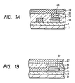
- Example 1 of the present invention will be described with reference to Figs. 1A and 1B and Figs. 2A to 2F.
- Fig. 1A illustrates a multi-layer wiring structure of an example in which first-layer metal wiring 21 and second-layer metal wiring 22 cross at right angles; and Fig. 1B, an example in which the first-layer metal wiring 21 and the second-layer metal wiring 22 are parallel.
- Both examples of Figs. 1A and 1B illustrate a two-layer wiring structure in which the first-layer metal wiring 21, an interlaminar insulating film 30 and the second-layer metal wiring 22 are provided on a backing 1 formed on a semiconductor substrate 2 and a terrace 10 is formed beneath a joining part 40 between the first-layer metal wiring 21 and second-layer metal wiring 22.
- a manufacturing process of the device of the present embodiment is shown in Figs. 2A to 2F.
- a silicon oxide film for example, is formed by deposition on the backing 1 formed on a silicon substrate 2 serving as the semiconductor substrate, so as to cover the whole surface of the semiconductor device.
- the above silicon oxide film is selectively removed to form the terrace 10 (Fig. 2A).
- etching is carried out using, for example, argon (Ar) gas, where edges of the terrace 10 are etched at a higher rate, so that the edges of the terrace 10 are rounded as shown in Fig. 2B.
- the first-layer metal wiring 21 comprised of, for example, aluminum (Al) is formed as shown in Fig. 2C.
- the interlaminar insulating film 30 comprised of, for example, a silicon oxide film is formed by deposition to have a larger film thickness than that of the terrace 10, and a leveling resist 52 is further coated so as to give a flat surface (Fig. 2D).
- the interlaminar insulating film 30 and the leveling resist 52 are subjected to dry etching at the same rate so that they are removed until a joining part 40 of the first-layer metal wiring 21 is uncovered as shown in Fig. 2E.
- the second-layer metal wiring 22 comprised of, for example, aluminum (Al) is formed.
- a multi-layer wiring structure as shown in Fig. 2F is thus formed.
- the terrace 10 is formed beneath the joining part 40.
- the position of the first-layer metal wiring 21 becomes higher only at the position of the joining part 40, and hence the area of contact between the first-layer metal wiring 21 and second-layer metal wiring 22 can be sufficiently secured without bringing about the disadvantage that the second-layer metal wiring 22 becomes smaller in thickness, and, in addition, the interlaminar insulating film 30 can assure sufficient insulation between the first-layer metal wiring 21 and second-layer metal wiring 22 at the region except the joining part 40.
- a good multi-layer wiring structure can be thus formed.
- the terrace 10 may also be formed of a conductive film of, for example, aluminum (Al). It thereby becomes possible to completely eliminate the disadvantage that the metal wiring layer becomes smaller in thickness at the joining part 40 and thus further improve the reliability.
- the width of the terrace 10 may be made larger than the width of the first-layer metal wiring 21. It thereby becomes possible to prevent troubles from occurring at the joining part 40 which are caused by the deviation of patterns when the terrace 10, first-layer metal wiring 21 and second-layer metal wiring 22 are each subjected to patterning.
- Example 2 of the present invention will be described with reference to Fig. 3 and Figs. 4A to 4F.
- a device isolation region 3 formed on a p-type semiconductor substrate 2 serves as a backing.
- a terrace 10 comprised of a gate electrode 11a covered with a covering oxide film 12 and a sidewall oxide film 14 is formed at the same time when a gate electrode 11b of a normal MOSFET formed beneath a joining part 40 by a conventional process is formed.
- the device isolation region 3 (with a film thickness of, for example, 600 nm) is formed on the p-type semiconductor substrate 2 by the LOCOS process (local oxidation process).
- a gate oxide film 4 (with a film thickness of, for example, 16 nm) is formed, and a gate electrode material comprising, for example, an n+-type polycrystalline silicon film (with a film thickness of, for example, 250 nm) and a silicon oxide film (with a film thickness of, for example, 200 nm) are further deposited.
- the above gate electrode material and the above silicon oxide film are selectively removed using a resist 51, so that the gate electrodes 11a and 11b and the covering oxide films 12 are formed as shown in Fig. 4A.
- the gate electrode 11a on the device isolation region 3 and the gate electrode 11b on the gate oxide film 4 are simultaneously formed.
- the gate electrode 11a is used as the terrace 10 for the formation of a multi-layer wiring structure in the subsequent step and the gate electrode 11b is used as a gate electrode of the normal MOSFET.
- the resist 51 is removed, and ions as exemplified by phosphate ions (P+) are implanted so that an n ⁇ -type semiconductor layer 5 is formed.
- a silicon oxide film 13 is formed by deposition as shown in Fig. 4B to have a given film thickness (for example, a film thickness of 250 nm), and then the silicon oxide film 13 is removed by anisotropic etching. As a result, a sidewall oxide film 14 with a width of about 250 nm is formed.
- the gate electrode 11a covered with an insulating film comprised of the covering oxide film 12 and the sidewall oxide film 14 constitutes the terrace 10 (with a total thickness of 450 nm in this example), and at the same time the slope of the side walls of the terrace 10 can be made gentle by virtue of the sidewall oxide film 14 (Fig. 4C).
- ions as exemplified by arsenate ions (As+) are implanted so that an n+-type semiconductor layer 6 serving as source and drain of the MOSFET is formed.
- an alloy of, for example, aluminum, silicon and copper hereinafter referred to as Al-Si-Cu alloy
- Al-Si-Cu alloy an alloy of, for example, aluminum, silicon and copper
- an interlaminar insulating film 30 comprised of, for example, a silicon oxide film is formed by deposition over the whole surface of the semiconductor device to have a larger thickness (with a film thickness of, for example, 2,000 nm) so that it becomes higher than the joining part 40 formed at the surface of the first-layer metal wiring 21.
- a leveling resist 52 is further coated (with a coating thickness of, for example, 1,500 nm) so as to give a flat surface (Fig. 4E).
- the interlaminar insulating film 30 and the leveling resist 52 are subjected to dry etching at the same rate so that they are removed until the joining part 40 at the surface of the first-layer metal wiring 21 positioned above the terrace 10 is uncovered as shown in Fig.
- a second-layer metal wiring 22 comprised of, for example, an Al-Si-Cu alloy is formed to give a multi-layer wiring structure as shown in Fig. 3.
- the area of contact between the first-layer metal wiring 21 and second-layer metal wiring 22 can be sufficiently secured without bringing about the disadvantage that the second-layer metal wiring 22 becomes smaller in thickness, and, in addition, the interlaminar insulating film 30 can assure sufficient insulation between the first-layer metal wiring 21 and second-layer metal wiring 22 at the region except the joining part 40.
- a good multi-layer wiring structure can be thus formed.
- the terrace 10 is formed at the same time when the MOSFET is formed, so that not only no increase in manufacturing steps is brought about for the formation of the terrace 10, but also the number of masks used can be reduced compared with conventional methods since the step of forming through-holes becomes unnecessary.
- the multi-layer wiring structure and the MOSFET are simultaneously formed but also the n+-type semiconductor layer 6 serving as source and drain of the MOSFET are joined in self-alignment without use of a mask.
- a silicon oxide film is used as the gate oxide film 4 of the MOSFET.
- the multi-layer wiring structure employing the terrace according to the present invention can also be applied in a MOSFET structure comprising an insulating film other than the silicon oxide film, as exemplified by a laminated film of a silicon oxide film and a silicon nitride film.
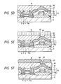
- Example 3 of the present invention will be described with reference to Figs. 5A to 5F.
- ions as exemplified by arsenate ions (As+) are implanted so that an n+-type semiconductor layer 6 serving as source and drain of the MOSFET is formed.
- a BPSG (borophosphosilicate glass) film 7 is formed by deposition over the whole surface of the semiconductor device to give a given film thickness (a film thickness of, for example, 350 nm), and then a suitable heat treatment (for example, at 900°C for 30 minutes) is applied to effect reflowing of the BPSG film 7 so that the form of the terrace on the surface can be made a little gentle.
- a suitable heat treatment for example, at 900°C for 30 minutes
- the BPSG film 7 is selectively etched using a mask to form a contact hole 8 on the source and drain and the gate electrode 11b (a contact hole with respect to a gate electrode 11a is not shown).
- an Al-Si-Cu alloy for example, is deposited over the whole surface, and a first-layer metal wiring 21 (with a film thickness of, for example, 800 nm) is formed as shown in Fig. 5B.
- an interlaminar insulating film 30 comprised of, for example, a silicon oxide film is formed by deposition over the whole surface of the semiconductor device to have a larger thickness (with a film thickness of, for example, 2,000 nm) so that it becomes higher than the joining part 40 formed at the surface of the first-layer metal wiring 21.
- a leveling resist 52 is further coated (with a coating thickness of, for example, 1,500 nm) so as to give a flat surface (Fig. 5C).
- the interlaminar insulating film 30 and the leveling resist 52 are subjected to dry etching at the same rate so that the interlaminar insulating film 30 is made flat to have a given thickness (for example, a film thickness of 600 nm on the first-layer metal wiring 21 formed on the flattened surface).
- the interlaminar insulating film 30 is made to remain on the whole surface of the semiconductor device, in other words, to remain also on the joining part 40 at the surface of the first-layer metal wiring 21 positioned above the terrace 10 (Fig. 5D).
- the interlaminar insulating film 30 is selectively removed using a resist 53 to form a through-hole 60 so that the joining part 40 of the first-layer metal wiring 21 is uncovered (Fig.
- a second-layer metal wiring 22 (with a film thickness of, for example, 1,000 nm) comprised of, for example, an Al-Si-Cu alloy is formed to give a multi-layer wiring structure as shown in Fig. 5F.
- the terrace 10 for making higher the position of the joining part 40 of the first-layer metal wiring 21 is used in combination with the through-hole 60 formed by selectively removing the interlaminar insulating film 30 by the use of a mask.
- the height of the terrace 10 can be reduced and also the aspect ratio of the through-hole can be made smaller, so that the first-layer metal wiring 21 and the second-layer metal wiring 22 may not become smaller in film thickness and the insulation between the first-layer metal wiring 21 and second-layer metal wiring 22 can be sufficiently ensured.
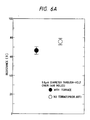
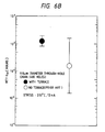
- the evaluation was made on a chain of through-holes (400 holes) of 0.8 ⁇ m in diameter, prepared exactly as described in this example, and electric characteristics were compared on whether or not the terrace 10 comprised of the gate electrode 11a of the MOSFET, insulated by the covering oxide film 12 and sidewall oxide film 14, is formed beneath the through-hole 60.
- Fig. 6A is a diagram showing initial resistance of the chain of through-holes.
- the formation of the terrace has resulted in a decrease by 12.7 % in the resistance of the chain, but with substantially the same standard deviation of the resistance.
- the yield of the chain in a wafer of 6 inch in diameter was 97.8 % (44/45) when the terrace is provided, and 84.4 % (38/45) when no terrace is provided.
- the second-layer Al-Si-Cu wiring can be buried in the through-hole in a greatly improved state when the terrace 10 is provided beneath the through-hole 10, and superior initial characteristics are exhibited in respect of the resistance and the yield.
- MTF Mean time to failure
- ⁇ standard deviation
- the terrace 10 is formed at the same time when the MOSFET is formed, so that no increase in manufacturing steps is brought about for the formation of the terrace 10.
- Example 4 of the present invention will be described with reference to Figs. 7A to 7D.
- a silicon nitride film 31 for example, is formed by deposition to have a given film thickness (for example, a film thickness of 200 nm).
- a silicon oxide film 32 for example, is formed by deposition over the whole surface of the semiconductor device to have a larger thickness (with a film thickness of, for example, 2,000 nm) so that it becomes higher than the joining part 40 formed at the surface of the first-layer metal wiring 21.
- An interlaminar insulating film 30 comprised of the silicon nitride film 31 and the silicon oxide film 32 is thus formed.
- a leveling resist 52 is further coated (with a coating thickness of, for example, 1,500 nm) so as to give a flat surface (Fig. 7A).
- the silicon oxide film 32 and the leveling resist 52 are subjected to dry etching at the same rate so that the surface of the silicon oxide film 32 is made flat, and the silicon oxide film 32 is further etched to the extent of a given thickness while the etching rate for the silicon oxide film 32 is made greater than that for the silicon nitride film 31 so that the silicon nitride film 31 is protrudingly uncovered as shown in Fig.
- the etching rate for the silicon oxide film 32 is made sufficiently greater than that for the silicon nitride film 31, it may not occur that the silicon nitride film 31 is removed and the surface of the first-layer metal wiring 21 is uncovered.
- the depth of a through-hole 60 formed in the subsequent step can be controlled in a good accuracy.
- the silicon nitride film 31 is selectively removed using a resist 53 as a mask, whereby the through-hole 60 can be formed in a smaller depth (a film thickness of 200 nm in the present embodiment) and the joining part 40 of the first-layer metal wiring 21 is uncovered.
- the resist 53 may not be used and instead the silicon oxide film 32 may be made to serve as a mask so that only the silicon nitride film 31 is removed and thus the joining part 40 is uncovered.
- a second-layer metal wiring 22 (with a film thickness of, for example, 1,000 nm) comprised of, for example, an Al-Si-Cu alloy is formed to give a multi-layer wiring structure as shown in Fig. 7D. As shown in Fig.
- the terrace 10 for making higher the position of the joining part 40 of the first-layer metal wiring 21 is used in combination with the through-hole 60 formed by selectively removing the lower-layer insulating film 31 of the interlaminar insulating film 30 by the use of a mask.
- the height of the terrace 10 can be reduced and also the aspect ratio of the through-hole can be made smaller, so that the first-layer metal wiring 21 and the second-layer metal wiring 22 may not become smaller in film thickness and the insulation between the first-layer metal wiring 21 and second-layer metal wiring 22 can be sufficiently ensured.
- the terrace 10 is formed at the same time when the MOSFET is formed, so that no increase in manufacturing steps is brought about for the formation of the terrace 10.
- the interlaminar insulating film 30 is formed in a laminated structure comprised of the silicon nitride film 31 and silicon oxide film 32, and the silicon nitride film 31 is selectively removed using a mask.
- the size of the opening at the joining part 40 can be controlled in an improved accuracy.
- the aspect ratio of the through-hole 60 can also be controlled depending on the film thickness of the silicon nitride film 31. Thus the aspect ratio can be made smaller with a decrease in film thickness of the silicon nitride film 31.
- Example 5 of the present invention will be described with reference to Fig. 8 and Figs. 9A to 9E.
- Fig. 8 shows a three-layer wiring structure comprised of a first-layer metal wiring 21, a second-layer metal wiring 22 and a third-layer metal wiring 23.
- a terrace 10 with the same constitution as a gate electrode of a MOSFET is formed beneath a joining part 40 between the first-layer metal wiring 21 and the third-layer metal wiring 23, and the three-layer metal wirings 21, 22 and 23 are connected each other through through-holes 60, 61a and 61b, respectively.
- a manufacturing process of the present embodiment is shown in Figs. 9A to 9E.
- the manufacturing steps up to the formation of a first interlaminar insulating film 33 comprised of a silicon nitride film 31 and a silicon oxide film 32 are the same as the steps up to the step shown in Fig. 78. Accordingly, descriptions on these steps are omitted.
- the silicon oxide film 32 and the silicon nitride film 31 are selectively removed using a resist 53 as a mask, thereby forming the through-hole 60 as shown in Fig. 9A.
- a second-layer metal wiring 22 (with a film thickness of, for example, 600 nm) comprised of, for example, an Al-Si-Cu alloy is formed as shown in Fig. 9B.
- a second interlaminar insulating film 34 comprised of, for example, a silicon oxide film is formed by deposition over the whole surface of the semiconductor device to have a large thickness (with a film thickness of, for example, 2,000 nm).
- a leveling resist 54 is further coated (with a coating thickness of, for example, 1,500 nm) so as to give a flat surface (Fig. 9C).
- the second interlaminar insulating film 34 and the leveling resist 54 are subjected to dry etching at the same rate so that the surface of the second interlaminar insulating film 34 is made flat as shown in Fig. 9D.
- the second interlaminar insulating film 34 and the silicon nitride film 31 are selectively etched so that the through-hole 61a on the first-layer metal wiring 21 and the through-hole 61b on the second-layer metal wiring 22 can be simultaneously formed (Fig. 9E).
- a third-layer metal wiring 23 (with a film thickness of, for example, 1,000 nm) comprised of, for example, an Al-Si-Cu alloy is formed to give a multi-layer wiring structure as shown in Fig. 8.
- the terrace 10 is so provided that the first-layer metal wiring 21 is in substantially the same level as the second-layer metal wiring 22 at the joining part 40.
- the first-layer metal wiring 21 and the second-layer metal wiring 22 to be simultaneously connected each other with the third-layer metal wiring 23.
- the through-hole 61a and the through-hole 61b can be made to have substantially the same smaller depth, and hence minute working can be carried out at a large tolerance, bringing about a remarkable increase in the degree of freedom in relation to the connection or joining between the three-layer wiring.
- Examples 1 to 4 are concerned with multi-layer wiring structures comprised of first-layer wiring and second-layer wiring
- Example 5 shows a structure comprised of first-layer wiring, second-layer wiring and third-layer wiring.
- the same results can also be obtained on a structure comprised of nth-layer wiring and n+mth-layer wiring (where n and m are each a natural number).
- an Al-Si-Cu alloy is used as the material in metal wiring.
- the device isolation region is formed by the LOCOS process, but the device isolation region may also be formed by the buried oxide process (BOX process).
- a silicon substrate is used as the semiconductor substrate, but it is also possible to use a Ge substrate, an oxide semiconductor substrate, and other semiconductor substrates.
Landscapes
- Internal Circuitry In Semiconductor Integrated Circuit Devices (AREA)
- Electrodes Of Semiconductors (AREA)
Applications Claiming Priority (2)
| Application Number | Priority Date | Filing Date | Title |
|---|---|---|---|
| JP17011589 | 1989-06-30 | ||
| JP170115/89 | 1989-06-30 |
Publications (2)
| Publication Number | Publication Date |
|---|---|
| EP0415526A2 true EP0415526A2 (de) | 1991-03-06 |
| EP0415526A3 EP0415526A3 (en) | 1991-11-21 |
Family
ID=15898917
Family Applications (1)
| Application Number | Title | Priority Date | Filing Date |
|---|---|---|---|
| EP19900307231 Withdrawn EP0415526A3 (en) | 1989-06-30 | 1990-07-02 | Semiconductor device having wiring layers |
Country Status (2)
| Country | Link |
|---|---|
| EP (1) | EP0415526A3 (de) |
| JP (1) | JPH04127452A (de) |
Cited By (3)
| Publication number | Priority date | Publication date | Assignee | Title |
|---|---|---|---|---|
| FR2672430A1 (fr) * | 1991-02-05 | 1992-08-07 | Samsung Electronics Co Ltd | Structure de contact intercouches d'un dispositif a semiconducteur et procede de fabrication de celle-ci. |
| DE4311509A1 (de) * | 1992-05-16 | 1993-11-18 | Gold Star Electronics | Verfahren zum Herstellen eines Halbleiterbauelements |
| FR2701336A1 (fr) * | 1991-10-29 | 1994-08-12 | Gen Electric | Structure d'interconnexion à densité élevée, puce de semiconducteur comprenant cette structure et procédé de fabrication. |
Families Citing this family (3)
| Publication number | Priority date | Publication date | Assignee | Title |
|---|---|---|---|---|
| US5861673A (en) * | 1995-11-16 | 1999-01-19 | Taiwan Semiconductor Manufacturing Company | Method for forming vias in multi-level integrated circuits, for use with multi-level metallizations |
| JP6690509B2 (ja) * | 2016-11-22 | 2020-04-28 | 株式会社村田製作所 | 半導体装置 |
| JP7052714B2 (ja) | 2018-12-27 | 2022-04-12 | 株式会社豊田自動織機 | 遠心圧縮機 |
Family Cites Families (2)
| Publication number | Priority date | Publication date | Assignee | Title |
|---|---|---|---|---|
| US4708767A (en) * | 1984-10-05 | 1987-11-24 | Signetics Corporation | Method for providing a semiconductor device with planarized contacts |
| JPH0644593B2 (ja) * | 1984-11-09 | 1994-06-08 | 株式会社東芝 | 半導体集積回路装置 |
-
1990
- 1990-06-29 JP JP2173484A patent/JPH04127452A/ja active Pending
- 1990-07-02 EP EP19900307231 patent/EP0415526A3/en not_active Withdrawn
Cited By (3)
| Publication number | Priority date | Publication date | Assignee | Title |
|---|---|---|---|---|
| FR2672430A1 (fr) * | 1991-02-05 | 1992-08-07 | Samsung Electronics Co Ltd | Structure de contact intercouches d'un dispositif a semiconducteur et procede de fabrication de celle-ci. |
| FR2701336A1 (fr) * | 1991-10-29 | 1994-08-12 | Gen Electric | Structure d'interconnexion à densité élevée, puce de semiconducteur comprenant cette structure et procédé de fabrication. |
| DE4311509A1 (de) * | 1992-05-16 | 1993-11-18 | Gold Star Electronics | Verfahren zum Herstellen eines Halbleiterbauelements |
Also Published As
| Publication number | Publication date |
|---|---|
| JPH04127452A (ja) | 1992-04-28 |
| EP0415526A3 (en) | 1991-11-21 |
Similar Documents
| Publication | Publication Date | Title |
|---|---|---|
| US4937652A (en) | Semiconductor device and method of manufacturing the same | |
| US5756396A (en) | Method of making a multi-layer wiring structure having conductive sidewall etch stoppers and a stacked plug interconnect | |
| US5470793A (en) | Method of via formation for the multilevel interconnect integrated circuits | |
| US5403777A (en) | Semiconductor bond pad structure and method | |
| JPH04290232A (ja) | 溝埋込み配線形成方法 | |
| JPS62279661A (ja) | 集積回路に貫通導体を形成する方法 | |
| JPH06125013A (ja) | 半導体装置及びその製造方法 | |
| EP0248668A2 (de) | Verfahren zum Herstellen von integrierten metallischen Mehrschicht-Schaltungen und gemäss diesem Verfahren hergestellte Strukturen | |
| JPH04229618A (ja) | 集積回路デバイスの接点及びその形成方法 | |
| US5296407A (en) | Method of manufacturing a contact structure for integrated circuits | |
| EP0415526A2 (de) | Halbleiteranordnung mit Leiterschichten | |
| US6133141A (en) | Methods of forming electrical connections between conductive layers | |
| JPH04290249A (ja) | 半導体装置の製造方法 | |
| JPH07254607A (ja) | 集積回路及びその製造方法 | |
| US5136361A (en) | Stratified interconnect structure for integrated circuits | |
| DE102005035771B4 (de) | Technik zur Herstellung einer Kontaktschicht auf Kupferbasis ohne ein Endmetall | |
| US5247204A (en) | Semiconductor device having multilayer interconnection structure | |
| US5282922A (en) | Hybrid circuit structures and methods of fabrication | |
| JPS60262443A (ja) | 多層配線の形成方法 | |
| JP2779186B2 (ja) | 半導体装置の製造方法 | |
| JPS63147346A (ja) | 半導体集積回路装置 | |
| JPH05299418A (ja) | 半導体装置の製造方法 | |
| JP3533022B2 (ja) | 半導体集積回路装置およびその製造方法 | |
| JPH0542139B2 (de) | ||
| JPH0917868A (ja) | 半導体集積回路装置の配線接続構造及びその製造方法 |
Legal Events
| Date | Code | Title | Description |
|---|---|---|---|
| PUAI | Public reference made under article 153(3) epc to a published international application that has entered the european phase |
Free format text: ORIGINAL CODE: 0009012 |
|
| 17P | Request for examination filed |
Effective date: 19900712 |
|
| AK | Designated contracting states |
Kind code of ref document: A2 Designated state(s): DE FR GB |
|
| PUAL | Search report despatched |
Free format text: ORIGINAL CODE: 0009013 |
|
| AK | Designated contracting states |
Kind code of ref document: A3 Designated state(s): DE FR GB |
|
| STAA | Information on the status of an ep patent application or granted ep patent |
Free format text: STATUS: THE APPLICATION HAS BEEN WITHDRAWN |
|
| 18W | Application withdrawn |
Withdrawal date: 19920928 |