EP0442752A1 - Métaux de grande pureté, procédé de fabrication et cible de pulvérisation les utilisant - Google Patents
Métaux de grande pureté, procédé de fabrication et cible de pulvérisation les utilisant Download PDFInfo
- Publication number
- EP0442752A1 EP0442752A1 EP91301234A EP91301234A EP0442752A1 EP 0442752 A1 EP0442752 A1 EP 0442752A1 EP 91301234 A EP91301234 A EP 91301234A EP 91301234 A EP91301234 A EP 91301234A EP 0442752 A1 EP0442752 A1 EP 0442752A1
- Authority
- EP
- European Patent Office
- Prior art keywords
- metal
- ppm
- highly purified
- semi
- wiring network
- Prior art date
- Legal status (The legal status is an assumption and is not a legal conclusion. Google has not performed a legal analysis and makes no representation as to the accuracy of the status listed.)
- Granted
Links
Images




Classifications
-
- C—CHEMISTRY; METALLURGY
- C22—METALLURGY; FERROUS OR NON-FERROUS ALLOYS; TREATMENT OF ALLOYS OR NON-FERROUS METALS
- C22B—PRODUCTION AND REFINING OF METALS; PRETREATMENT OF RAW MATERIALS
- C22B34/00—Obtaining refractory metals
- C22B34/10—Obtaining titanium, zirconium or hafnium
- C22B34/12—Obtaining titanium or titanium compounds from ores or scrap by metallurgical processing; preparation of titanium compounds from other titanium compounds see C01G23/00 - C01G23/08
- C22B34/1263—Obtaining titanium or titanium compounds from ores or scrap by metallurgical processing; preparation of titanium compounds from other titanium compounds see C01G23/00 - C01G23/08 obtaining metallic titanium from titanium compounds, e.g. by reduction
- C22B34/1268—Obtaining titanium or titanium compounds from ores or scrap by metallurgical processing; preparation of titanium compounds from other titanium compounds see C01G23/00 - C01G23/08 obtaining metallic titanium from titanium compounds, e.g. by reduction using alkali or alkaline-earth metals or amalgams
- C22B34/1272—Obtaining titanium or titanium compounds from ores or scrap by metallurgical processing; preparation of titanium compounds from other titanium compounds see C01G23/00 - C01G23/08 obtaining metallic titanium from titanium compounds, e.g. by reduction using alkali or alkaline-earth metals or amalgams reduction of titanium halides, e.g. Kroll process
-
- C—CHEMISTRY; METALLURGY
- C22—METALLURGY; FERROUS OR NON-FERROUS ALLOYS; TREATMENT OF ALLOYS OR NON-FERROUS METALS
- C22B—PRODUCTION AND REFINING OF METALS; PRETREATMENT OF RAW MATERIALS
- C22B34/00—Obtaining refractory metals
- C22B34/10—Obtaining titanium, zirconium or hafnium
-
- C—CHEMISTRY; METALLURGY
- C22—METALLURGY; FERROUS OR NON-FERROUS ALLOYS; TREATMENT OF ALLOYS OR NON-FERROUS METALS
- C22B—PRODUCTION AND REFINING OF METALS; PRETREATMENT OF RAW MATERIALS
- C22B34/00—Obtaining refractory metals
- C22B34/10—Obtaining titanium, zirconium or hafnium
- C22B34/12—Obtaining titanium or titanium compounds from ores or scrap by metallurgical processing; preparation of titanium compounds from other titanium compounds see C01G23/00 - C01G23/08
- C22B34/129—Obtaining titanium or titanium compounds from ores or scrap by metallurgical processing; preparation of titanium compounds from other titanium compounds see C01G23/00 - C01G23/08 obtaining metallic titanium from titanium compounds by dissociation, e.g. thermic dissociation of titanium tetraiodide, or by electrolysis or with the use of an electric arc
-
- C—CHEMISTRY; METALLURGY
- C22—METALLURGY; FERROUS OR NON-FERROUS ALLOYS; TREATMENT OF ALLOYS OR NON-FERROUS METALS
- C22B—PRODUCTION AND REFINING OF METALS; PRETREATMENT OF RAW MATERIALS
- C22B34/00—Obtaining refractory metals
- C22B34/10—Obtaining titanium, zirconium or hafnium
- C22B34/12—Obtaining titanium or titanium compounds from ores or scrap by metallurgical processing; preparation of titanium compounds from other titanium compounds see C01G23/00 - C01G23/08
- C22B34/1295—Refining, melting, remelting, working up of titanium
-
- C—CHEMISTRY; METALLURGY
- C22—METALLURGY; FERROUS OR NON-FERROUS ALLOYS; TREATMENT OF ALLOYS OR NON-FERROUS METALS
- C22B—PRODUCTION AND REFINING OF METALS; PRETREATMENT OF RAW MATERIALS
- C22B9/00—General processes of refining or remelting of metals; Apparatus for electroslag or arc remelting of metals
- C22B9/16—Remelting metals
- C22B9/22—Remelting metals with heating by wave energy or particle radiation
-
- C—CHEMISTRY; METALLURGY
- C23—COATING METALLIC MATERIAL; COATING MATERIAL WITH METALLIC MATERIAL; CHEMICAL SURFACE TREATMENT; DIFFUSION TREATMENT OF METALLIC MATERIAL; COATING BY VACUUM EVAPORATION, BY SPUTTERING, BY ION IMPLANTATION OR BY CHEMICAL VAPOUR DEPOSITION, IN GENERAL; INHIBITING CORROSION OF METALLIC MATERIAL OR INCRUSTATION IN GENERAL
- C23C—COATING METALLIC MATERIAL; COATING MATERIAL WITH METALLIC MATERIAL; SURFACE TREATMENT OF METALLIC MATERIAL BY DIFFUSION INTO THE SURFACE, BY CHEMICAL CONVERSION OR SUBSTITUTION; COATING BY VACUUM EVAPORATION, BY SPUTTERING, BY ION IMPLANTATION OR BY CHEMICAL VAPOUR DEPOSITION, IN GENERAL
- C23C14/00—Coating by vacuum evaporation, by sputtering or by ion implantation of the coating forming material
- C23C14/22—Coating by vacuum evaporation, by sputtering or by ion implantation of the coating forming material characterised by the process of coating
- C23C14/34—Sputtering
- C23C14/3407—Cathode assembly for sputtering apparatus, e.g. Target
- C23C14/3414—Metallurgical or chemical aspects of target preparation, e.g. casting, powder metallurgy
-
- H—ELECTRICITY
- H10—SEMICONDUCTOR DEVICES; ELECTRIC SOLID-STATE DEVICES NOT OTHERWISE PROVIDED FOR
- H10D—INORGANIC ELECTRIC SEMICONDUCTOR DEVICES
- H10D64/00—Electrodes of devices having potential barriers
- H10D64/01—Manufacture or treatment
- H10D64/011—Manufacture or treatment of electrodes ohmically coupled to a semiconductor
- H10D64/0111—Manufacture or treatment of electrodes ohmically coupled to a semiconductor to Group IV semiconductors
- H10D64/0112—Manufacture or treatment of electrodes ohmically coupled to a semiconductor to Group IV semiconductors using conductive layers comprising silicides
-
- H—ELECTRICITY
- H10—SEMICONDUCTOR DEVICES; ELECTRIC SOLID-STATE DEVICES NOT OTHERWISE PROVIDED FOR
- H10P—GENERIC PROCESSES OR APPARATUS FOR THE MANUFACTURE OR TREATMENT OF DEVICES COVERED BY CLASS H10
- H10P14/00—Formation of materials, e.g. in the shape of layers or pillars
- H10P14/40—Formation of materials, e.g. in the shape of layers or pillars of conductive or resistive materials
- H10P14/42—Formation of materials, e.g. in the shape of layers or pillars of conductive or resistive materials using a gas or vapour
- H10P14/44—Physical vapour deposition [PVD]
-
- H—ELECTRICITY
- H10—SEMICONDUCTOR DEVICES; ELECTRIC SOLID-STATE DEVICES NOT OTHERWISE PROVIDED FOR
- H10W—GENERIC PACKAGES, INTERCONNECTIONS, CONNECTORS OR OTHER CONSTRUCTIONAL DETAILS OF DEVICES COVERED BY CLASS H10
- H10W20/00—Interconnections in chips, wafers or substrates
- H10W20/01—Manufacture or treatment
- H10W20/031—Manufacture or treatment of conductive parts of the interconnections
- H10W20/032—Manufacture or treatment of conductive parts of the interconnections of conductive barrier, adhesion or liner layers
-
- H—ELECTRICITY
- H10—SEMICONDUCTOR DEVICES; ELECTRIC SOLID-STATE DEVICES NOT OTHERWISE PROVIDED FOR
- H10W—GENERIC PACKAGES, INTERCONNECTIONS, CONNECTORS OR OTHER CONSTRUCTIONAL DETAILS OF DEVICES COVERED BY CLASS H10
- H10W20/00—Interconnections in chips, wafers or substrates
- H10W20/40—Interconnections external to wafers or substrates, e.g. back-end-of-line [BEOL] metallisations or vias connecting to gate electrodes
- H10W20/41—Interconnections external to wafers or substrates, e.g. back-end-of-line [BEOL] metallisations or vias connecting to gate electrodes characterised by their conductive parts
- H10W20/44—Conductive materials thereof
- H10W20/4403—Conductive materials thereof based on metals, e.g. alloys, metal silicides
- H10W20/4437—Conductive materials thereof based on metals, e.g. alloys, metal silicides the principal metal being a transition metal
- H10W20/4441—Conductive materials thereof based on metals, e.g. alloys, metal silicides the principal metal being a transition metal the principal metal being a refractory metal
Definitions
- the present invention relates to a highly purified metal suitable as a target material for the formation of electrode, contact part and barrier layer of a semi-conductor device, a method for the manufacture of the same and a sputtering target using the same.
- a silicide of a metal having a high melting point such as Mo, W, Ta, Ti, Zr and Hf have been used. Further, because there is a tendency of furthering high integration of semi-conductor devices and calling for more minute wiring structures, the possibility of various problems has been watched with misgivings.
- a Ti silicide when intended for use as the material for electrode, a Ti film is formed over a polysilicon film by the sputtering process. Then the Ti film is heat-treated to make a slicide out of Ti. What is called a polycide structure prepared in this way has been put to use.
- a contact part is inlaid with, for example a Ti film serving as a diffusion barrier layer in order to prevent Si from precipitating into Al wirings. In this sense, a laminated structure of Al/TiN/TiSi2 has been used.
- a TiN film is formed of a reactive sputtering material and the like.
- a TiN film or a TiSi2 film is made by the sputtering process. Therefore, the sputtering target required for the process must be made of a Ti material. It is important that the Ti target for that purpose has a high purity. When a Ti target contains an impurity of oxygen, the film formed therefrom has high electric resistance, causing a trouble of delay of signals or burn-out of wirings. Further, a heavy metal such as Fe, Ni and Cr collects on the interface of a laminated film and form a deep level, causing leakage at the joint thereof. An alkali metal such as Na and K readily sets Si free, deteriorating the properties of the device.
- a Ti material for the above mentioned Ti target generally is manufactured according to the so-called Kroll method or Hunter method to thermally reduce a Ti compound such as TiCl4 with an active metal such as Na and Mg or the fused salt electrolysis process using a fused salt consisting of alkaline metal compound.
- Kroll method or Hunter method to thermally reduce a Ti compound such as TiCl4 with an active metal such as Na and Mg or the fused salt electrolysis process using a fused salt consisting of alkaline metal compound.
- an object of the present invention is to provide a highly purified metal for the production of an electrode and a contact part capable of preventing malfunctions thereof in a highly integrated semi-conductor device and for the formation of a barrier layer capable of sufficiently preventing an increase of leakage at the junction.
- Another object of the present invention is to provide a method for the manufacture of highly purified metal making it possible to manufacture well reproducible a highly purified metal having the above mentioned properties.
- Still another object of the present invention is to provided a sputtering target capable of forming well reproducibly an electrode, a contact part, a barrier layer and the like respectively having high fidelity.
- the present inventors have gone ahead with the researches of impurities contained in target materials of Ti, Zr, Hf and the like, resulting in the findings that the above mentioned problems are accounted for by Al which has not been given much thought among other impurities of conventional targets.
- Al has been brought to light that the Al content need be lowered as much as possible on top of that of heavy and alkali metals, when an electrode, a contact part, a barrier layer and the like of a semi-conductor device are made of a target of Ti and the like according to the sputtering method.
- the Al content cannot be sufficiently reduced according to conventional manufacturing methods, remaining at a level such as 2000 ppm if it is a high side and finding no place as a forming material for highly integrated semi-conductor devices.
- the highly purified metal of the present invention has been achieved on the basis of the above mentioned finding and is characterized by having a Al content of not more than 10 ppm.
- the sputtering target of the present invention is characterized in that it is made by molding the above mentioned highly purified metal into a desired form.
- the highly purified metal is made by comprising one element selected from the group consisted of Ti, Zr and Hf.
- the highly purified metal is useful as a wiring material for use in LSI, VLSI, ULSI and the like.
- a wiring network of the present invention to be formed on a substrate in a semi-conductor device is characterized by containing 10ppm or less of Al and, specifically speaking, comprising a silicide, a nitride and the like of metals mentioned above.
- the wiring network like this can be obtained, for example according to the undermentioned production method.
- This is a production method comprising a step of forming a thin film from the sputtering target on a substrate in a semi-conductor device and a step of subjecting the thin film to etching treatment to eliminate portions other than the desired wiring network.
- the wiring network comprises an electrode, a contact part and a barrier layer of a semi-conductor device.
- the metal having a least possible Al content of the present invention has been brought to completion by the finding that the Al content can be efficiently reduced according to the iodide process and that Al contained in crude Ti particles and the like by the fused salt electrolysis process is converged and stays on the particle surface region and can be efficiently removed by the application of surface treatment technology.
- the first method for the manufacture of highly purified metal of the present invention comprises the steps of purifying crude metals according to the iodide process and a step of melting the so purified metals with an electron beam in a high vacuum.
- the second method for the manufacture comprises the steps of surface-treating crude metals produced under the fused salt electrolysis process and removing a contaminated layer from their surface and a step of melting the surface treated-crude metals with an electron beam in a high vacuum.
- the present invention provides an easy method for obtaining well reproducibly such a metal as Ti material, Zr material and Hf material respectively highly purified with a least possible Al content.
- a metal film and a metal compound film respectively having a low Al content can be well reproducibly formed by using said metal as a target material of the sputtering method, serving for an electrode, a contact part, a barrier layer and the like of a highly integrated semi-conductor device and contributing much to the promotion of semi-conductor device fidelity.
- Fig. 1 shows an example of the purifying apparatus of the iodide process for use in the present invention.
- Fig. 2 is to describe the structure of a diode prepared in one embodiment of the present invention.
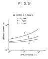
- Fig. 3 shows the relationship of the Al content of a Ti target prepared in one embodiment of the present invention with the leakage current of a diode having a TiSi2 film formed of said Ti target.
- Fig. 4 shows the relationship of the Al content of a Zr target prepared in one embodiment of the present invention with the leakage current of a diode having a ZrSi2 film formed of said Zr target.
- Fig. 5 shows the relationship of the Al content of a Hf target prepared in one embodiment of the present invention with the leakage current of a diode having a HfSi2 film formed of said Hf target.
- Fig. 6 shows the relationship of Ti film prepared in one embodiment of the present invention with specific resistance of a TiSi2 film formed of said Ti film.
- Fig. 7 relates to the fused salt electrolysis process used in one embodiment of the present invention, showing the relationship of the distance between the surface of the electrolyte and the location of a Ti material made therefrom with the Al content of said Ti material.
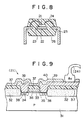
- Fig. 8 is a cross-section outlining the structure of a semi-conductor package obtained in connection with one embodiment of the present invention.
- Fig. 9 is a cross-section outlining the structure of a semi-conductor chip used in the semi-conductor package shown in Fig. 8.
- the highly purified metal that is the highly purified Ti material, the highly purified Zr material and the highly purified Hf material should have an Al content of not more than 10 ppm but the content of other impurities is at a low level as well.
- the oxygen content is not more than 250 ppm
- each of the Fe, Ni and Cr contents is not more than 100 ppm
- each of the Na and K contents is not more than 0.1 ppm.
- the U and Th contents preferably are not more than 0.001 ppm.
- the highly purified metal of the present invention is obtained by the application of either first or second manufacturing method as above mentioned.
- the first manufacturing method is to purify crude metals at first according to the iodide process.
- the iodide process will be described taking Ti as an example and referring to Fig. 1.
- Fig. 1 shows an example of a purification apparatus to purify Ti materials by means of the iodide process.
- Inside an electric furnace 2 there is a reaction container 1 receiving a crude Ti material and an iodine and within the reaction container 1 a filament 5 is set, connected with an electric source 4 via connecting plugs, 3a and 3b.
- the iodide process method is a system of chemical delivery, capable of purifying Ti by using the reactions represented by formulae (1) and (2):
- the crude Ti material and the iodine are placed in the reaction container 1 and the filament 5 is electrically charged and heated to a temperature of 1100 °C-1500 °C to keep the inside of the reaction container 1 at 100 °C-250 °C or 450 °C-600 °C.
- the crude Ti material and the iodine are reacted each other according to the formula (1) to form TiI4. Since the TiI4 is a volatile substance, it is decomposed into a Ti and an iodine again according to the formula (2), allowing the Ti alone to precipitate on the filament 5.
- the almost elements having less reactive than Ti among impurities of the material remains in the rest of the material. If the impurity easily reacts with the iodine to form iodides, the element having low steam pressure is not incorporated into the filament in the above temperature of the reaction container. If the iodide has suffient stream pressure, incorporation into the filament is prevented by controlling the pressure within the reaction container and dissociation temperature.
- the iodide decomposition method takes advantage that the content of the specific impurity is electively reduced by controlling the temperature of the reaction container, the pressure within the container, the temperature of the filament and the like. Since Al is sufficiently less reactive with iodine than Ti in the range of the temperature within the reaction container shown in the above formula (I), Al can be effectively removed from Ti. Thus, during the process of production and dissociation reaction, Ti is purified, thereby to provide a Ti material with a least possible Al content. In this case, it is important to select as a material one having a low Al content, and select as a material of reaction container one having low Al content. The same is true of Zr and Hf.
- the above mentioned iodide process can be operated by using as a starting material crude Ti materials which are obtained by various manufacturing methods such as Kroll process, Hunter process, fused salt electrolysis process and the like, but it is preferable to use therefor a Ti material produced by the fused salt electrolysis process.
- the purification of crude metals by the above mentioned iodide process is followed by melting the so purified materials with an electron beam (hereinafter referred to as "EB melting") in a high vacuum of not more than 5 x 10 ⁇ 5 mbar in order to finally remove Al, Na and K and to obtain a highly purified metal.
- EB melting is a method for the separation of impurities using a difference of vapor pressure and highly efficient in removing particularly Al, Na and K each having a high vapor pressure.
- Various metals are subjected to the EB melting , keeping a vacuum preferably not more than 5 x 10 ⁇ 5 mbar, more preferably not more than 2 x 10 ⁇ 5 mbar in the EB melting furnace, while preventing the entrance of a diffusion pump oil into said furnace with the use of a freon baffle.
- the operating conditions of EB melting are not particularly limited, but it is required that a melting speed should be determined taking into consideration the efficiency of purifying Na and K and the contamination due to the oxygen absorption. For example, a melting speed of 1.75 kg/hr - 2.3 kg/hr is preferable.
- a filament with a precipitated metal can be used as an electrode for the EB melting as it is.
- metals of Ti, Zr and Hf purified by the iodide process are subjected to the further purification according to the EB melting. Since said melting is implemented in a vacuum assuring less contamination due to oxygen and nitrogen, metals of high purity can be obtained.
- crude metal particles are prepared at first according to the fused salt electrolysis process.
- sponge Ti is used as a starting material therefore.
- an electrolyte comprising KCl-NaCl and the like is preferable.
- the electrolytic temperature is preferably 730 ° C-755 °C and the voltage 6.0V-8.0V.
- crude metals such as crude Ti particle contain impurities of metal elements including Al and oxygen which are converged in the neighborhood of the particle surface, the contaminated layer on the surface should be selectively removed.
- This contaminated surface layer is removed by, for example (1) a method for surface treating said layer with an acid or an alkali and (2) a method for volatilizing and removing said layer with such halogen as iodine, fluorine, chlorine and bromine.
- the above mentioned method (1) is preferably implemented in an atmosphere of such inactive gas such as argon gas to prevent the surface layer from recontamination particularly due to oxygen, conducting washing with purified water and drying afterwards.
- the treatment solution to be used therefor is an acidic solution such as hydrofluoric acid, nitric acid, sulfuric acid and their mixture or an alkaline solution such as a sodium hydroxide solution.
- an acidic solution such as hydrofluoric acid, nitric acid, sulfuric acid and their mixture or an alkaline solution such as a sodium hydroxide solution.
- heavy metals can easily be eliminated by the fused salt electrolysis process and it is possible to attempt to remove selectively Al alone as it is existing in the neighborhood of the surface.
- the use of sulfuric acid or sodium hydroxide solution is efficient in this case.
- the above mentioned method (2) is carried out as follows: a crude metal material obtained by the fused salt electrolysis process is placed in the purification apparatus using the iodide process as shown in Fig. 1, gaseous halogen is introduced thereto, a temperature elevated to a prescribed level is maintained inside the reaction container for a prescribed span of time, the surface of the crude metal is allowed to react with said halogen and then the product formed thereby is removed with suction.
- the reaction container has a sufficiently high temperature, almost all halides of metallic impurities are easily carried away out of the container because of their high vapor pressure.
- the contaminated surface layer of the crude metal is gradually removed by implementing this procedure repeatedly.
- the contaminated surface layer preferably more than 5 ⁇ m deep, more preferably more than 10 ⁇ m deep from the surface is removed by these methods.
- the content of impurities including Al can be relatively reduced by selecting and using Ti particles and the like of a comparatively small particle diameter which have smaller specific area. This helps in efficient removal of the contaminated surface layer.
- the substantially same effect can be achieved by sieving particles after the removal of their contaminated surface layer and selectively using those of comparatively larger particle diameter.
- the EB melting is employed in a high vacuum similar to the above mentioned first method in order to finally remove Al, Na, K and the like and obtain a highly purified metal.
- the Ti particles previously obtained should be compressed into a solid by a molding press and that the so obtained solid should be used as an electrode for the EB melting. In this case, however, recontamination on account of deformation incidental to molding is likely.
- the above mentioned removal treatment of the contaminated surface layer of metals obtained by the fused salt electrolysis process can be efficiently applied in the case where Ti materials obtained by the fused salt electrolysis process are used as a starting material for the first manufacturing method.
- a Ti material obtained by the fused salt electrolysis process wherein the contaminated surface layer thereof was subjected to surface treatment is purified by the iodide process at first. Then, the so purified is EB melted. In this way, the iodide process is allowed to achieve even higher purification efficiency.
- pretreat incidental to the iodide process can be done in one same apparatus, the above mentioned (2) is preferably used.
- Metals obtained according to either the first or second method have a Al content of satisfying not more than 10 ppm, an reduced content of other impurities and a high purity to a satisfaction.
- the oxygen content is not more than 250 ppm (preferably not more than 200 ppm)
- each of the Fe, Ni and Cr contents is not more than 10 ppm (preferably not more than 5 ppm each) and each of the Na and K contents is not more than 0.1 ppm (preferably not more than 0.05 ppm each).
- sputtering targets of the present invention are obtained by cold-forging the highly purified Ti material, the highly purified Zr material pr the highly purified Hf material into a desired shape, while preventing their recontamination.
- Said cold-forging is carried out in a cold condition (at about room temperature), taking into consideration the properties of, for example the Ti material with high gas absorption and the feasibility of preventing recontamination due to gas absorption.
- the processibility improved by satisfying a high purity makes cold-working possible. This is followed by machine-working of target materials to provide sputtering targets in a prescribed shape.
- Sponge Ti was manufactured according to the Kroll process in order to use it as a starting crude Ti material.
- the so obtained sponge Ti was set in the reaction container 1 of the purification apparatus using the iodide process, as shown in Fig. 1 and the amount of an iodine representing a ratio of 0.2 g/l was also placed therein.
- Said sponge Ti was purified by the iodide process under the conditions that the temperature of the filament 5 was maintained at 1400 °C and that of the reaction container 1 at 600 °C.
- the filament 5 had a diameter of 2 mm when the purification was started and Ti was allowed to precipitate thereon until the diameter was increased to about 30 mm.
- the figment with precipitated Ti was used as a starting material for EB melting to conduct the EB melting under the conditions of a high vacuum of 1 x 10 ⁇ 5 mbar in the furnace, preventing the entrance of diffusion pump oil into the furnace with the use of freon baffle, a voltage of 20 kV, a filament current of 1.5A-2.0A, a EB output of 30 KW-40 KW and a melting speed of 4 kg/hr.
- ingots having a diameter of 135 mm respectively obtained.
- Embodiment 1 The substantially same procedures for the iodide process and EB melting as in Embodiment 1 were repeated except that the crude Ti material of said Embodiment 1 was replaced by Ti in a shape of needle obtained by the fused salt electrolysis process and Ti ingots obtained therefrom were processed to produce Ti targets. The so obtained Ti targets were analyzed, resulting in the determinations also shown in Table 1.
- needle shaped-Ti of the fused salt electrolysis process which had been used as the crude Ti material in above Embodiment 2 was immersed in a mixture of hydrofluoric acid, nitric acid and water in a ratio of 2:1:1 for 10 minutes in order to remove the contaminated surface layer.
- the so treated needle shaped-Ti was washed with running water to make a starting Ti material. Meanwhile, the contaminated surface layer 15 ⁇ m deep from the surface was removed.
- the iodide process and the EB melting were implemented according to the same procedure as in Embodiment 1, except that above acid treated Ti material was used and the Ti ingots obtained therefrom were further processed to make Ti targets.
- the so obtained Ti targets were analyzed, resulting in the determinations shown in Table 1 as well.
- the needle shaped Ti which had been used as the crude Ti material in Embodiment 2 was placed, a gaseous iodine was introduced therein after vacuum exhaust, the temperature was maintained at 600 °C and the surface of the needle shaped Ti was allowed to react with the iodine. Then, the reaction product was eliminated by vacuum exhaust. This procedure was repeated 3 times to remove the contaminated surface layer. The contaminated surface layer 15 ⁇ m deep from the surface was removed. Meanwhile, the used purification apparatus had an exhaust system connected with the reaction container via an iodide trapping mechanism which is missing in the illustration.
- the filament 5 was electrically charged, the iodide process and the EB melting were carried out and Ti ingots were obtained. Then, Ti targets were made thereof. The so obtained targets were analyzed, resulting in the determinations shown in Fig. 1 as well.
- the Ti materials of all the above mentioned embodiments have a low content of Al that should adversely affect the properties of electrode, contact part, barrier layers and the like in a semi-conductor device, keeping the content of other impurities at a reduced level and satisfying the purity as it should be.
- a Ti film, a Zr film and a Hf film, each 60 nm thick were respectively formed by the sputtering method using each of 3 types of Ti target, Zr target and Hf target which were produced according to substantially the same procedure as in the corresponding embodiment and each type of which has different Al content.
- each film was treated by etching to remove portions other than the desired wiring network, the remaining film was subjected to 2 step annealing treatment to comprise a silicide and form a metal silicide film (TiSi2 film, ZrSi2 film, HfSi2) over the polycrystal Si layer 12 and at the same time both the source region 14 and the drain region 15 were made to comprise a silicide and the diode of each metal silicide film was produced.
- a metal silicide film TiSi2 film, ZrSi2 film, HfSi2
- Each type of Ti target contained Al in an amount of not more than 54 ppm, 3 ppm and 1 ppm; that of Zr target not more than 68 ppm, 3 ppm and 1 ppm; and that of Hf target not more than 70 ppm, 2ppm and 1 ppm. Other impurities contained in these targets were in an equal amount.
- the leakage current was measured by applying an inverse bias voltage to the so obtained diodes to obtain the results respectively in Fig. 3, Fig. 4 and Fig. 5.
- an electrode, a contact part and the like having a high fidelity for a highly integrated semi-conductor device can be accomplished by making a sputtering target of a metal having a low Al content as obtained in the above mentioned embodiments, producing a metal target of said sputtering target and forming a desired form therefrom.
- TiSi2 films can be reduced by decreasing the oxygen content of Ti targets. Further, specific resistance of TiSi2 films can also be lowered by lowering specific resistance of Ti films. Particularly, TiSi2 having as low specific resistance as 15 ⁇ .cm are not obtained by using Ti targets having an oxygen content of more than 250 ppm.
- a TiSi2 film having low resistance means the prevention of delay of signals in a semi-conductor device to make possible a semi-conductor device having high fidelity.
- An electrode made of sponge Ti was placed in an electrolyte comprising KCl-NaCl (KCl: 16% by weight, NaCl: 84% by weight) and subjected to fused salt electrolysis process at an electrolytic temperature of 755 °C, a current of 200A and a voltage of 80V in order to produce a crude needle-shaped Ti particle.
- the contaminated surface layer of these crude needle-shaped Ti materials was removed by means of an aqueous solution of hydrochloric acid.
- Said acid treatment was conducted by immersing the crude Ti materials in said aqueous solution of hydrochloric acid in an argon gas atmosphere for each different from span of time and then they were washed with purified water and dried.
- the crude Ti particles immersed in the acid for different spans of time were used as a starting material for EB melting and placed in a vibrating granulator.
- Said granulator was introduced into an EB melting furnace in a vacuum, while preventing the contamination.
- EB melting was conducted under the conditions of a high vacuum of 1 x 10 ⁇ 5 mbar in the furnace, preventing the entrance of diffusion pump oil into the furnace with a freon baffle, voltage of 20KV, a filament current of 1.3A-1.5A, an EB output of 26KW-30KW and a meltin g speed of 4 kg/h in order to make ingots having a diameter of 135 mm.
- each of the so obtained Ti materials was analyzed for impurities.
- the relationship between the Al content and the amount of the removal by acid treatment is shown in Table 3.
- each of the Fe, Ni and Cr contents was not more than 1 ppm
- each of the Na and K contents was not more than 0.01 ppm
- the oxygen content was not more than 200 ppm.
- the embodiment showed that the Ti material having a satisfactorily high purity, a low content of Al adversely affecting the properties of electrode, contact part and barrier layer of semi-conductor devices and a reduced content of other purities was obtained by removing the surface layer from the crude Ti material and then Eb melting it.
- Fig. 7 is a drawing outlining the structure of one instance of the semi-conductor package.
- 21 is a semi-conductor chip set on an insulation substrate 22 by a solder layer 23.
- the semi-conductor chip 21 is electrically connected with a lead frame 25 by a Au lead wire 25.
- the semi-conductor chip 21, Au lead wire 24 and lead frame 25 are sealed together in a molding by a sealing resin 26.
- the semi-conductor chip 21 comprises the highly purified metal of the present invention and is used as the material for a part of the wiring network.
- the semi-conductor chip 21 and the method for producing the same will be described referring to Fig. 9.
- a p-Si substrate 31 is treated by thermal oxidation to form a thermally oxidized film on the surface of p-Si substrate.
- a field oxidized film 32 is optionally formed by thermal oxidation except for the source and drain regions. Portions of the thermally oxidized film on each of the source and drain regions were eliminated by formation of a resist film and etching treatment (hereinafter called PEP treatment for short) to give a thermally oxidized film 33 remaining on the gate region.
- PEP treatment etching treatment
- a Mo or W silicide film 36 is formed on the gate oxidized film 33.
- An insulation layer 37 comprising P-doped silica glass (PSG) is formed all over the p-Si substrate and then both the source region 34 and the drain region 35 were subjected to PEP treatment to remove portions of the P-doped silica glass layer 37 located thereon.
- PSG P-doped silica glass
- barrier layer 38 is formed respectively on the source region 34 and the drain region 35 after portions of the P-doped silica glass layer 37 are removed therefrom.
- These barrier layers 38 are the film comprising the highly purified metal of the present invention. Namely, substantially the same materials as Ti target, Zr target and Hf target used in the above mentioned embodiment are treated by the reactive sputtering method in an nitrogen gas atmosphere to produce a TiN film, a ZrN film, a HfN film each of which contains Al in a very small amount and is used to form the barrier layer 38.
- an Al film 39 is formed by vacuum evaporation to cover the whole surface and obtain the wiring network in a desired shape. Further, an insulating protection film 40 comprising Si3N4 and the like is formed all over, a portion thereof is subjected to PEP treatment to build an opening for bonding of the Au lead wire (24) and finally an semi-conductor chip (21) is complete.
- the barrier layer which is sound even when the wiring network is densely formed can be obtained by producing the TiN film, ZrN film and Hf film from the highly purified metal of the present invention. This is because content of impurities inside the barrier layer 38 can be controlled to be very small, including that of Al, oxygen, alkali and heavy metals, and as a result the semi-conductor package having the high operational reliability can be obtained.
Landscapes
- Chemical & Material Sciences (AREA)
- Engineering & Computer Science (AREA)
- Organic Chemistry (AREA)
- Metallurgy (AREA)
- Materials Engineering (AREA)
- Mechanical Engineering (AREA)
- Manufacturing & Machinery (AREA)
- Life Sciences & Earth Sciences (AREA)
- Environmental & Geological Engineering (AREA)
- General Life Sciences & Earth Sciences (AREA)
- Geology (AREA)
- Physics & Mathematics (AREA)
- Plasma & Fusion (AREA)
- Chemical Kinetics & Catalysis (AREA)
- Manufacture And Refinement Of Metals (AREA)
- Physical Vapour Deposition (AREA)
- Electrodes Of Semiconductors (AREA)
Priority Applications (3)
| Application Number | Priority Date | Filing Date | Title |
|---|---|---|---|
| EP98204064A EP0915176A1 (fr) | 1990-02-15 | 1991-02-15 | Câblage du réseau et empaquetage de semi-conducteur |
| EP98204068A EP0915178A3 (fr) | 1990-02-15 | 1991-02-15 | Cible de pulvérisation en titane de haute pureté |
| EP98204065A EP0915177B1 (fr) | 1990-02-15 | 1991-02-15 | Hafnium de grande pureté et cible de pulvérisation l'utilisant |
Applications Claiming Priority (3)
| Application Number | Priority Date | Filing Date | Title |
|---|---|---|---|
| JP3690890 | 1990-02-15 | ||
| JP36908/90 | 1990-02-15 | ||
| JP3690890 | 1990-02-15 |
Related Child Applications (3)
| Application Number | Title | Priority Date | Filing Date |
|---|---|---|---|
| EP98204064A Division EP0915176A1 (fr) | 1990-02-15 | 1991-02-15 | Câblage du réseau et empaquetage de semi-conducteur |
| EP98204068A Division EP0915178A3 (fr) | 1990-02-15 | 1991-02-15 | Cible de pulvérisation en titane de haute pureté |
| EP98204065A Division EP0915177B1 (fr) | 1990-02-15 | 1991-02-15 | Hafnium de grande pureté et cible de pulvérisation l'utilisant |
Publications (2)
| Publication Number | Publication Date |
|---|---|
| EP0442752A1 true EP0442752A1 (fr) | 1991-08-21 |
| EP0442752B1 EP0442752B1 (fr) | 2001-01-10 |
Family
ID=12482879
Family Applications (4)
| Application Number | Title | Priority Date | Filing Date |
|---|---|---|---|
| EP98204068A Ceased EP0915178A3 (fr) | 1990-02-15 | 1991-02-15 | Cible de pulvérisation en titane de haute pureté |
| EP91301234A Expired - Lifetime EP0442752B1 (fr) | 1990-02-15 | 1991-02-15 | Procédé de fabrication de titane de grande pureté et d'une cible de pulvérisation cathodique |
| EP98204064A Withdrawn EP0915176A1 (fr) | 1990-02-15 | 1991-02-15 | Câblage du réseau et empaquetage de semi-conducteur |
| EP98204065A Expired - Lifetime EP0915177B1 (fr) | 1990-02-15 | 1991-02-15 | Hafnium de grande pureté et cible de pulvérisation l'utilisant |
Family Applications Before (1)
| Application Number | Title | Priority Date | Filing Date |
|---|---|---|---|
| EP98204068A Ceased EP0915178A3 (fr) | 1990-02-15 | 1991-02-15 | Cible de pulvérisation en titane de haute pureté |
Family Applications After (2)
| Application Number | Title | Priority Date | Filing Date |
|---|---|---|---|
| EP98204064A Withdrawn EP0915176A1 (fr) | 1990-02-15 | 1991-02-15 | Câblage du réseau et empaquetage de semi-conducteur |
| EP98204065A Expired - Lifetime EP0915177B1 (fr) | 1990-02-15 | 1991-02-15 | Hafnium de grande pureté et cible de pulvérisation l'utilisant |
Country Status (4)
| Country | Link |
|---|---|
| US (3) | US5196916A (fr) |
| EP (4) | EP0915178A3 (fr) |
| KR (1) | KR940008936B1 (fr) |
| DE (2) | DE69133267T2 (fr) |
Cited By (18)
| Publication number | Priority date | Publication date | Assignee | Title |
|---|---|---|---|---|
| EP0555085A1 (fr) * | 1992-02-05 | 1993-08-11 | Kabushiki Kaisha Toshiba | Cible de pulvérisation |
| EP0574119A2 (fr) * | 1992-04-21 | 1993-12-15 | Kabushiki Kaisha Toshiba | Cible en Ti-W pour pulvérisation cathodique et procédé pour sa fabrication |
| FR2756572A1 (fr) * | 1996-12-04 | 1998-06-05 | Pechiney Aluminium | Alliages d'aluminium a temperature de recristallisation elevee utilisee dans les cibles de pulverisation cathodiques |
| US6024847A (en) * | 1997-04-30 | 2000-02-15 | The Alta Group, Inc. | Apparatus for producing titanium crystal and titanium |
| US6063254A (en) * | 1997-04-30 | 2000-05-16 | The Alta Group, Inc. | Method for producing titanium crystal and titanium |
| US6309595B1 (en) | 1997-04-30 | 2001-10-30 | The Altalgroup, Inc | Titanium crystal and titanium |
| WO2002029125A1 (fr) * | 2000-10-02 | 2002-04-11 | Nikko Materials Company, Limited | Zirconium ou hafnium extremement purs, cible de pulverisation composee de ce zirconium ou hafnium extremement purs, couche mince obtenue au moyen de cette cible, procede de preparation de zirconium ou de hafnium extremement purs et procede de fabrication d'une poudre de zirconium ou de hafnium extremement purs |
| WO2003006702A1 (fr) * | 2001-07-09 | 2003-01-23 | Nikko Materials Company, Limited | Cible de siliciure d'hafnium servant a former un film d'oxyde de grille et son procede de production |
| WO2002061168A3 (fr) * | 2000-10-24 | 2003-03-13 | Honeywell Int Inc | Procedes de preparation de materiaux metalliques melanges a base de titane et a base de zirconium et cibles de pulverisation |
| WO2004016825A1 (fr) * | 2002-08-06 | 2004-02-26 | Nikko Materials Co., Ltd. | Cible en siliciure de hafnium et son procede de preparation |
| WO2004079039A1 (fr) * | 2003-03-07 | 2004-09-16 | Nikko Materials Co., Ltd. | Cible en alliage d'hafnium et son procede de production |
| RU2291214C2 (ru) * | 2004-11-29 | 2007-01-10 | Открытое акционерное общество "ТВЭЛ" (ОАО ТВЭЛ) | Способ йодидного рафинирования гафния |
| WO2007007498A1 (fr) * | 2005-07-07 | 2007-01-18 | Nippon Mining & Metals Co., Ltd. | Hafnium de grande pureté, cible et couche mince comprenant de l'hafnium de grande pureté et procédé de production d'hafnium de grande pureté |
| EP1652944A4 (fr) * | 2003-07-25 | 2007-05-23 | Nippon Mining Co | Materiau en hafnium tres pur, film mince de cible comprenant ce materiau et procede de production de hafnium tres pur |
| RU2353687C1 (ru) * | 2007-10-31 | 2009-04-27 | Открытое акционерное общество "Чепецкий механический завод" (ОАО ЧМЗ) | Аппарат для йодидного рафинированного гафния |
| CN105632745A (zh) * | 2014-10-27 | 2016-06-01 | 国家电网公司 | 一种用于变压器的半导体导电材料的生产工艺 |
| CN111154978A (zh) * | 2019-12-30 | 2020-05-15 | 江智秦 | 一种稀有金属碘化提纯方法 |
| CN112725641A (zh) * | 2019-10-15 | 2021-04-30 | 有研资源环境技术研究院(北京)有限公司 | 一种高纯金属钒的制备方法 |
Families Citing this family (28)
| Publication number | Priority date | Publication date | Assignee | Title |
|---|---|---|---|---|
| JPS62280335A (ja) * | 1986-05-30 | 1987-12-05 | Toshiba Corp | 薄膜形成用高純度チタン材、それを用いて形成されてなるターゲットおよび薄膜、および薄膜形成用高純度チタン材の製造方法 |
| KR940008936B1 (ko) * | 1990-02-15 | 1994-09-28 | 가부시끼가이샤 도시바 | 고순도 금속재와 그 성질을 이용한 반도체 장치 및 그 제조방법 |
| KR970009274B1 (ko) * | 1991-11-11 | 1997-06-09 | 미쓰비시덴키 가부시키가이샤 | 반도체장치의 도전층접속구조 및 그 제조방법 |
| US5849417A (en) * | 1994-09-12 | 1998-12-15 | Japan Energy Corporation | Titanium implantation materials for the living body |
| DE19609439A1 (de) * | 1995-03-14 | 1996-09-19 | Japan Energy Corp | Verfahren zum Erzeugen von hochreinem Kobalt und Sputtering-Targets aus hochreinem Kobalt |
| JP3413782B2 (ja) * | 1995-03-31 | 2003-06-09 | 日立金属株式会社 | スパッタリング用チタンタ−ゲットおよびその製造方法 |
| JP2679680B2 (ja) * | 1995-04-24 | 1997-11-19 | 日本電気株式会社 | 半導体装置の製造方法 |
| JPH0923005A (ja) * | 1995-07-06 | 1997-01-21 | Mitsubishi Electric Corp | 半導体装置およびその製造方法 |
| JP2863469B2 (ja) * | 1995-10-06 | 1999-03-03 | 株式会社住友シチックス尼崎 | 高純度チタン材の製造方法 |
| US5612558A (en) | 1995-11-15 | 1997-03-18 | Micron Technology, Inc. | Hemispherical grained silicon on refractory metal nitride |
| JPH10330932A (ja) * | 1997-05-28 | 1998-12-15 | Anelva Corp | スパッタリング装置 |
| US6001227A (en) | 1997-11-26 | 1999-12-14 | Applied Materials, Inc. | Target for use in magnetron sputtering of aluminum for forming metallization films having low defect densities and methods for manufacturing and using such target |
| US6139701A (en) * | 1997-11-26 | 2000-10-31 | Applied Materials, Inc. | Copper target for sputter deposition |
| JPH11269621A (ja) | 1997-12-24 | 1999-10-05 | Toho Titanium Co Ltd | 高純度チタン材の加工方法 |
| US6348113B1 (en) | 1998-11-25 | 2002-02-19 | Cabot Corporation | High purity tantalum, products containing the same, and methods of making the same |
| TWI230741B (en) * | 1999-11-22 | 2005-04-11 | Nikko Materials Co Ltd | Titanium sputtering target |
| JP2001279432A (ja) * | 2000-01-27 | 2001-10-10 | Mitsui Mining & Smelting Co Ltd | 低酸素スパッタリングターゲット |
| JP3995082B2 (ja) * | 2001-07-18 | 2007-10-24 | 日鉱金属株式会社 | ゲート酸化膜形成用ハフニウムシリサイドターゲット及びその製造方法 |
| JP4388263B2 (ja) * | 2002-09-11 | 2009-12-24 | 日鉱金属株式会社 | 珪化鉄スパッタリングターゲット及びその製造方法 |
| CN101760647A (zh) * | 2003-11-19 | 2010-06-30 | 日矿金属株式会社 | 高纯度铪的制造方法 |
| EP1559485A1 (fr) * | 2004-01-30 | 2005-08-03 | Siemens Aktiengesellschaft | Procédé pour l'enlèvement d'une couche |
| LV13528B (en) * | 2006-09-25 | 2007-03-20 | Ervins Blumbergs | Method and apparatus for continuous producing of metallic tifanium and titanium-bases alloys |
| KR101047495B1 (ko) * | 2009-11-18 | 2011-07-07 | 한국기계연구원 | 고순도 지르코늄 금속분말의 제조방법, 및 이에 의한 고순도 지르코늄 금속분말의 제조장치 |
| KR20160064232A (ko) | 2012-02-14 | 2016-06-07 | 제이엑스금속주식회사 | 고순도 티탄 잉곳, 그 제조 방법 및 티탄 스퍼터링 타깃 |
| CN103713169B (zh) * | 2013-12-23 | 2016-09-21 | 上海金陵智能电表有限公司 | 一种感应式电能表 |
| KR20180085059A (ko) | 2014-03-31 | 2018-07-25 | 가부시끼가이샤 도시바 | 스퍼터링 타깃의 제조 방법 및 스퍼터링 타깃 |
| US10287175B1 (en) * | 2015-12-30 | 2019-05-14 | L'Air Liquide Société Anonyme pour l'Etude et l'Exploitation des Procédés Georges Claude | Method for purification and storage of Til4 for Ti-containing film deposition |
| WO2024049324A1 (fr) * | 2022-08-29 | 2024-03-07 | Акционерное общество "Чепецкий механический завод" | Procédé de production de hafnium selon un procédé de raffinage d'iodure |
Citations (4)
| Publication number | Priority date | Publication date | Assignee | Title |
|---|---|---|---|---|
| DE1130604B (de) * | 1956-03-13 | 1962-05-30 | Ici Ltd | Verfahren zur Herstellung von Titan |
| EP0248338A1 (fr) * | 1986-05-30 | 1987-12-09 | Kabushiki Kaisha Toshiba | Titane très pur et son procédé d'obtention |
| EP0316580A1 (fr) * | 1987-10-22 | 1989-05-24 | Westinghouse Electric Corporation | Procédé de fabrication d'alliages ultra-purs à base de zirconium-étain pour revêtement intérieure d'éléments combustibles pour réacteur nucléaire |
| EP0408383A1 (fr) * | 1989-07-14 | 1991-01-16 | Kabushiki Kaisha Toshiba | Titane hautement purifié, son procédé de fabrication et cible de pulvérisation l'utilisant |
Family Cites Families (29)
| Publication number | Priority date | Publication date | Assignee | Title |
|---|---|---|---|---|
| US3654526A (en) * | 1970-05-19 | 1972-04-04 | Texas Instruments Inc | Metallization system for semiconductors |
| FR2359221A1 (fr) * | 1976-07-23 | 1978-02-17 | Anvar | Procede de fabrication de titane par reduction electrolytique dans un bain de sels fondus d'halogenures de titane |
| US4368072A (en) * | 1979-03-12 | 1983-01-11 | Teledyne Industries, Inc. | Iodide cell vapor pressure control |
| JPS5830147A (ja) * | 1981-08-18 | 1983-02-22 | Toshiba Corp | 半導体装置 |
| JPS6066425A (ja) * | 1983-09-22 | 1985-04-16 | Nippon Telegr & Teleph Corp <Ntt> | Lsi電極用の高純度モリブデンタ−ゲツトならびに高純度モリブデンシリサイドタ−ゲツトおよびその製造方法 |
| JPH0697667B2 (ja) * | 1983-10-21 | 1994-11-30 | セイコーエプソン株式会社 | 半導体装置の製造方法 |
| JPS60208430A (ja) * | 1984-03-30 | 1985-10-21 | Toyo Soda Mfg Co Ltd | 金属沃化物から高純度金属の製造法 |
| JPS61143530A (ja) * | 1984-12-17 | 1986-07-01 | Nippon Nuclear Fuel Dev Co Ltd | 高純度ジルコニウムの製造方法 |
| US4725872A (en) * | 1985-02-25 | 1988-02-16 | Tektronix, Inc. | Fast channel single phase buried channel CCD |
| CA1216962A (fr) * | 1985-06-28 | 1987-01-20 | Hussein M. Naguib | Methode de fabrication de dispositifs mos |
| JPH0611076B2 (ja) * | 1985-10-08 | 1994-02-09 | 三菱電機株式会社 | 半導体装置の製造方法 |
| JPH062588B2 (ja) * | 1986-02-12 | 1994-01-12 | 東ソー株式会社 | 超高純度沃化チタンの製造方法 |
| JPS6373660A (ja) * | 1986-09-17 | 1988-04-04 | Fujitsu Ltd | 半導体装置 |
| JPS6381948A (ja) * | 1986-09-26 | 1988-04-12 | Toshiba Corp | 多層配線半導体装置 |
| US4782380A (en) * | 1987-01-22 | 1988-11-01 | Advanced Micro Devices, Inc. | Multilayer interconnection for integrated circuit structure having two or more conductive metal layers |
| JPS63230834A (ja) * | 1987-03-20 | 1988-09-27 | Hitachi Metals Ltd | 高温反応室内観察窓 |
| US4788160A (en) * | 1987-03-31 | 1988-11-29 | Texas Instruments Incorporated | Process for formation of shallow silicided junctions |
| US5019891A (en) * | 1988-01-20 | 1991-05-28 | Hitachi, Ltd. | Semiconductor device and method of fabricating the same |
| US5027185A (en) * | 1988-06-06 | 1991-06-25 | Industrial Technology Research Institute | Polycide gate FET with salicide |
| JPH0622218B2 (ja) * | 1988-08-06 | 1994-03-23 | 富士通株式会社 | エッチング方法 |
| US4897287A (en) * | 1988-10-06 | 1990-01-30 | The Boc Group, Inc. | Metallization process for an integrated circuit |
| KR930004295B1 (ko) * | 1988-12-24 | 1993-05-22 | 삼성전자 주식회사 | Vlsi 장치의 n+ 및 p+ 저항영역에 저저항 접속방법 |
| JP2537413B2 (ja) * | 1989-03-14 | 1996-09-25 | 三菱電機株式会社 | 半導体装置およびその製造方法 |
| US4997518A (en) * | 1989-03-31 | 1991-03-05 | Oki Electric Industry Co., Ltd. | Method for forming an electrode layer by a laser flow technique |
| US4920073A (en) * | 1989-05-11 | 1990-04-24 | Texas Instruments, Incorporated | Selective silicidation process using a titanium nitride protective layer |
| KR940008936B1 (ko) * | 1990-02-15 | 1994-09-28 | 가부시끼가이샤 도시바 | 고순도 금속재와 그 성질을 이용한 반도체 장치 및 그 제조방법 |
| US5175126A (en) * | 1990-12-27 | 1992-12-29 | Intel Corporation | Process of making titanium nitride barrier layer |
| US5345108A (en) * | 1991-02-26 | 1994-09-06 | Nec Corporation | Semiconductor device having multi-layer electrode wiring |
| EP0545327A1 (fr) * | 1991-12-02 | 1993-06-09 | Matsushita Electric Industrial Co., Ltd. | Réseau de transistors à couche mince pour une utilisation dans un afficheur à cristaux liquides |
-
1991
- 1991-02-13 KR KR1019910002583A patent/KR940008936B1/ko not_active Expired - Lifetime
- 1991-02-15 DE DE69133267T patent/DE69133267T2/de not_active Expired - Fee Related
- 1991-02-15 EP EP98204068A patent/EP0915178A3/fr not_active Ceased
- 1991-02-15 EP EP91301234A patent/EP0442752B1/fr not_active Expired - Lifetime
- 1991-02-15 EP EP98204064A patent/EP0915176A1/fr not_active Withdrawn
- 1991-02-15 US US07/655,950 patent/US5196916A/en not_active Expired - Lifetime
- 1991-02-15 EP EP98204065A patent/EP0915177B1/fr not_active Expired - Lifetime
- 1991-02-15 DE DE69132504T patent/DE69132504T2/de not_active Expired - Fee Related
-
1994
- 1994-12-07 US US08/351,542 patent/US5458697A/en not_active Expired - Lifetime
-
1995
- 1995-05-31 US US08/454,583 patent/US5679983A/en not_active Expired - Fee Related
Patent Citations (4)
| Publication number | Priority date | Publication date | Assignee | Title |
|---|---|---|---|---|
| DE1130604B (de) * | 1956-03-13 | 1962-05-30 | Ici Ltd | Verfahren zur Herstellung von Titan |
| EP0248338A1 (fr) * | 1986-05-30 | 1987-12-09 | Kabushiki Kaisha Toshiba | Titane très pur et son procédé d'obtention |
| EP0316580A1 (fr) * | 1987-10-22 | 1989-05-24 | Westinghouse Electric Corporation | Procédé de fabrication d'alliages ultra-purs à base de zirconium-étain pour revêtement intérieure d'éléments combustibles pour réacteur nucléaire |
| EP0408383A1 (fr) * | 1989-07-14 | 1991-01-16 | Kabushiki Kaisha Toshiba | Titane hautement purifié, son procédé de fabrication et cible de pulvérisation l'utilisant |
Non-Patent Citations (2)
| Title |
|---|
| PATENT ABSTRACTS OF JAPAN vol. 10, no. 339 (C-385)(2395), 15 November 1986; & JP-A-61 143 530 (NIPPON NUCLEAR FUEL DEV. CO.) 01.07.1986 * |
| WINKLER et al.: "VACUUM METALLURGY" 1971, pages 270,271, Elsevier Publishing Company, London, GB * |
Cited By (31)
| Publication number | Priority date | Publication date | Assignee | Title |
|---|---|---|---|---|
| EP0555085A1 (fr) * | 1992-02-05 | 1993-08-11 | Kabushiki Kaisha Toshiba | Cible de pulvérisation |
| US5418071A (en) * | 1992-02-05 | 1995-05-23 | Kabushiki Kaisha Toshiba | Sputtering target and method of manufacturing the same |
| EP0735159A1 (fr) * | 1992-02-05 | 1996-10-02 | Kabushiki Kaisha Toshiba | Cible de pulvérisation cathodique |
| EP0574119A2 (fr) * | 1992-04-21 | 1993-12-15 | Kabushiki Kaisha Toshiba | Cible en Ti-W pour pulvérisation cathodique et procédé pour sa fabrication |
| US6264813B1 (en) | 1996-12-04 | 2001-07-24 | Aluminum Pechiney | Cathodic sputtering targets made of aluminum alloy |
| WO1998024945A1 (fr) * | 1996-12-04 | 1998-06-11 | Aluminium Pechiney | Cibles de pulverisation cathodique en alliage d'aluminium |
| FR2756572A1 (fr) * | 1996-12-04 | 1998-06-05 | Pechiney Aluminium | Alliages d'aluminium a temperature de recristallisation elevee utilisee dans les cibles de pulverisation cathodiques |
| US6024847A (en) * | 1997-04-30 | 2000-02-15 | The Alta Group, Inc. | Apparatus for producing titanium crystal and titanium |
| US6063254A (en) * | 1997-04-30 | 2000-05-16 | The Alta Group, Inc. | Method for producing titanium crystal and titanium |
| US6309595B1 (en) | 1997-04-30 | 2001-10-30 | The Altalgroup, Inc | Titanium crystal and titanium |
| US6596228B2 (en) | 1997-04-30 | 2003-07-22 | Honeywell International Inc. | Titanium materials |
| WO2002029125A1 (fr) * | 2000-10-02 | 2002-04-11 | Nikko Materials Company, Limited | Zirconium ou hafnium extremement purs, cible de pulverisation composee de ce zirconium ou hafnium extremement purs, couche mince obtenue au moyen de cette cible, procede de preparation de zirconium ou de hafnium extremement purs et procede de fabrication d'une poudre de zirconium ou de hafnium extremement purs |
| EP1743949A1 (fr) | 2000-10-02 | 2007-01-17 | Nippon Mining & Metals Co., Ltd. | Fabrication de zirconium ou d'hafnium à haute pureté en forme métallique ou particulaire pour cibles de pulvérisation et films minces |
| US6833058B1 (en) | 2000-10-24 | 2004-12-21 | Honeywell International Inc. | Titanium-based and zirconium-based mixed materials and sputtering targets |
| WO2002061168A3 (fr) * | 2000-10-24 | 2003-03-13 | Honeywell Int Inc | Procedes de preparation de materiaux metalliques melanges a base de titane et a base de zirconium et cibles de pulverisation |
| WO2003006702A1 (fr) * | 2001-07-09 | 2003-01-23 | Nikko Materials Company, Limited | Cible de siliciure d'hafnium servant a former un film d'oxyde de grille et son procede de production |
| WO2004016825A1 (fr) * | 2002-08-06 | 2004-02-26 | Nikko Materials Co., Ltd. | Cible en siliciure de hafnium et son procede de preparation |
| US6986834B2 (en) | 2002-08-06 | 2006-01-17 | Nikko Materials Co., Ltd. | Hafnium silicide target and manufacturing method for preparation thereof |
| CN100335676C (zh) * | 2002-08-06 | 2007-09-05 | 日矿金属株式会社 | 硅化铪靶及其制造方法 |
| EP1602745A4 (fr) * | 2003-03-07 | 2009-05-27 | Nippon Mining Co | Cible en alliage d'hafnium et son procede de production |
| WO2004079039A1 (fr) * | 2003-03-07 | 2004-09-16 | Nikko Materials Co., Ltd. | Cible en alliage d'hafnium et son procede de production |
| CN100445420C (zh) * | 2003-03-07 | 2008-12-24 | 日矿金属株式会社 | 铪合金靶及其制造方法 |
| EP1652944A4 (fr) * | 2003-07-25 | 2007-05-23 | Nippon Mining Co | Materiau en hafnium tres pur, film mince de cible comprenant ce materiau et procede de production de hafnium tres pur |
| RU2291214C2 (ru) * | 2004-11-29 | 2007-01-10 | Открытое акционерное общество "ТВЭЛ" (ОАО ТВЭЛ) | Способ йодидного рафинирования гафния |
| WO2007007498A1 (fr) * | 2005-07-07 | 2007-01-18 | Nippon Mining & Metals Co., Ltd. | Hafnium de grande pureté, cible et couche mince comprenant de l'hafnium de grande pureté et procédé de production d'hafnium de grande pureté |
| EP1930451A4 (fr) * | 2005-07-07 | 2009-08-19 | Nippon Mining Co | Hafnium de grande pureté, cible et couche mince comprenant de l'hafnium de grande pureté et procédé de production d'hafnium de grande pureté |
| KR100968396B1 (ko) * | 2005-07-07 | 2010-07-07 | 닛코 킨조쿠 가부시키가이샤 | 고순도 하프늄, 고순도 하프늄으로 이루어지는 타겟 및박막 그리고 고순도 하프늄의 제조 방법 |
| RU2353687C1 (ru) * | 2007-10-31 | 2009-04-27 | Открытое акционерное общество "Чепецкий механический завод" (ОАО ЧМЗ) | Аппарат для йодидного рафинированного гафния |
| CN105632745A (zh) * | 2014-10-27 | 2016-06-01 | 国家电网公司 | 一种用于变压器的半导体导电材料的生产工艺 |
| CN112725641A (zh) * | 2019-10-15 | 2021-04-30 | 有研资源环境技术研究院(北京)有限公司 | 一种高纯金属钒的制备方法 |
| CN111154978A (zh) * | 2019-12-30 | 2020-05-15 | 江智秦 | 一种稀有金属碘化提纯方法 |
Also Published As
| Publication number | Publication date |
|---|---|
| DE69133267T2 (de) | 2004-04-08 |
| DE69132504T2 (de) | 2001-06-07 |
| DE69132504D1 (de) | 2001-02-15 |
| KR940008936B1 (ko) | 1994-09-28 |
| EP0442752B1 (fr) | 2001-01-10 |
| EP0915178A2 (fr) | 1999-05-12 |
| US5196916A (en) | 1993-03-23 |
| EP0915176A1 (fr) | 1999-05-12 |
| DE69133267D1 (de) | 2003-06-26 |
| US5458697A (en) | 1995-10-17 |
| KR920000112A (ko) | 1992-01-10 |
| EP0915177A1 (fr) | 1999-05-12 |
| EP0915178A3 (fr) | 1999-05-26 |
| EP0915177B1 (fr) | 2003-05-21 |
| US5679983A (en) | 1997-10-21 |
Similar Documents
| Publication | Publication Date | Title |
|---|---|---|
| US5458697A (en) | Highly purified metal material and sputtering target using the same | |
| KR910009316B1 (ko) | 실리콘 함유 금속층을 선택적으로 형성하는 방법 | |
| EP0377137B1 (fr) | Procédé de dépÔt sélectif de métal réfractaire sur des substrats de silicium | |
| US4605479A (en) | In-situ cleaned ohmic contacts | |
| KR100239608B1 (ko) | 반도체 웨이퍼상에 규화 티타늄을 형성시키는 단일 어닐링 방법 | |
| US5126283A (en) | Process for the selective encapsulation of an electrically conductive structure in a semiconductor device | |
| US5221853A (en) | MOSFET with a refractory metal film, a silicide film and a nitride film formed on and in contact with a source, drain and gate region | |
| JP2921799B2 (ja) | 半導体素子形成用高純度スパッタターゲットの製造方法 | |
| EP0720214A2 (fr) | Procédé de traitement de films de nitrures métalliques pour diminuer la migration de silicium | |
| KR960030339A (ko) | 반도체장치 및 그 제조공정 | |
| EP0471845A1 (fr) | Procede de formation d'une pellicule d'oxyde de silicium | |
| EP0725429A2 (fr) | Procédé de formation d'une couche de fluorure de métal pour un dispositif électronique | |
| JP3228660B2 (ja) | 半導体素子形成用高純度金属材の製造方法 | |
| JP3103527B2 (ja) | 半導体素子形成用配線膜および半導体パッケージ | |
| JPH0860350A (ja) | 高純度金属材の製造方法、スパッタターゲットの製造方法および配線網の形成方法 | |
| JP3621582B2 (ja) | スパッタターゲット | |
| JPH10317073A (ja) | 半導体素子形成用配線膜および半導体パッケージ | |
| JPH07114203B2 (ja) | 半導体装置の製造方法 | |
| JPH0666286B2 (ja) | シリコン含有金属膜の形成方法 | |
| JPH0813141A (ja) | スパッタリングターゲット及びその製造方法 | |
| JPH02139932A (ja) | 半導体装置の製造方法 | |
| JPH07142411A (ja) | 半導体装置における金属薄膜形成方法 | |
| JPH01253241A (ja) | 半導体装置の製造方法 | |
| EP0496637A2 (fr) | Films conducteur de grande pureté et leur utilisation dans les semi-conducteurs | |
| JPH0433129B2 (fr) |
Legal Events
| Date | Code | Title | Description |
|---|---|---|---|
| PUAI | Public reference made under article 153(3) epc to a published international application that has entered the european phase |
Free format text: ORIGINAL CODE: 0009012 |
|
| 17P | Request for examination filed |
Effective date: 19910306 |
|
| AK | Designated contracting states |
Kind code of ref document: A1 Designated state(s): DE FR GB |
|
| 17Q | First examination report despatched |
Effective date: 19940609 |
|
| GRAG | Despatch of communication of intention to grant |
Free format text: ORIGINAL CODE: EPIDOS AGRA |
|
| RIC1 | Information provided on ipc code assigned before grant |
Free format text: 7C 22B 34/12 A, 7H 01J 37/02 B, 7H 05K 1/09 B |
|
| RTI1 | Title (correction) |
Free format text: METHOD OF MANUFACTURING A HIGHLY PURIFIED TITANIUM METAL AND A SPUTTERING TARGET |
|
| GRAG | Despatch of communication of intention to grant |
Free format text: ORIGINAL CODE: EPIDOS AGRA |
|
| GRAH | Despatch of communication of intention to grant a patent |
Free format text: ORIGINAL CODE: EPIDOS IGRA |
|
| GRAH | Despatch of communication of intention to grant a patent |
Free format text: ORIGINAL CODE: EPIDOS IGRA |
|
| GRAA | (expected) grant |
Free format text: ORIGINAL CODE: 0009210 |
|
| AK | Designated contracting states |
Kind code of ref document: B1 Designated state(s): DE FR GB |
|
| REF | Corresponds to: |
Ref document number: 69132504 Country of ref document: DE Date of ref document: 20010215 |
|
| ET | Fr: translation filed | ||
| PLBE | No opposition filed within time limit |
Free format text: ORIGINAL CODE: 0009261 |
|
| STAA | Information on the status of an ep patent application or granted ep patent |
Free format text: STATUS: NO OPPOSITION FILED WITHIN TIME LIMIT |
|
| REG | Reference to a national code |
Ref country code: GB Ref legal event code: IF02 |
|
| 26N | No opposition filed | ||
| PGFP | Annual fee paid to national office [announced via postgrant information from national office to epo] |
Ref country code: FR Payment date: 20030210 Year of fee payment: 13 |
|
| PGFP | Annual fee paid to national office [announced via postgrant information from national office to epo] |
Ref country code: GB Payment date: 20030212 Year of fee payment: 13 |
|
| PGFP | Annual fee paid to national office [announced via postgrant information from national office to epo] |
Ref country code: DE Payment date: 20030227 Year of fee payment: 13 |
|
| PG25 | Lapsed in a contracting state [announced via postgrant information from national office to epo] |
Ref country code: GB Free format text: LAPSE BECAUSE OF NON-PAYMENT OF DUE FEES Effective date: 20040215 |
|
| PG25 | Lapsed in a contracting state [announced via postgrant information from national office to epo] |
Ref country code: DE Free format text: LAPSE BECAUSE OF NON-PAYMENT OF DUE FEES Effective date: 20040901 |
|
| GBPC | Gb: european patent ceased through non-payment of renewal fee |
Effective date: 20040215 |
|
| PG25 | Lapsed in a contracting state [announced via postgrant information from national office to epo] |
Ref country code: FR Free format text: LAPSE BECAUSE OF NON-PAYMENT OF DUE FEES Effective date: 20041029 |
|
| REG | Reference to a national code |
Ref country code: FR Ref legal event code: ST |