EP0459836B1 - Verfahren zum Herstellen von Dünnfilmtransistoren - Google Patents
Verfahren zum Herstellen von Dünnfilmtransistoren Download PDFInfo
- Publication number
- EP0459836B1 EP0459836B1 EP91305013A EP91305013A EP0459836B1 EP 0459836 B1 EP0459836 B1 EP 0459836B1 EP 91305013 A EP91305013 A EP 91305013A EP 91305013 A EP91305013 A EP 91305013A EP 0459836 B1 EP0459836 B1 EP 0459836B1
- Authority
- EP
- European Patent Office
- Prior art keywords
- source
- drain
- layers
- semiconductor layer
- single crystal
- Prior art date
- Legal status (The legal status is an assumption and is not a legal conclusion. Google has not performed a legal analysis and makes no representation as to the accuracy of the status listed.)
- Expired - Lifetime
Links
Images

Classifications
-
- H—ELECTRICITY
- H10—SEMICONDUCTOR DEVICES; ELECTRIC SOLID-STATE DEVICES NOT OTHERWISE PROVIDED FOR
- H10P—GENERIC PROCESSES OR APPARATUS FOR THE MANUFACTURE OR TREATMENT OF DEVICES COVERED BY CLASS H10
- H10P14/00—Formation of materials, e.g. in the shape of layers or pillars
- H10P14/20—Formation of materials, e.g. in the shape of layers or pillars of semiconductor materials
- H10P14/38—Formation of materials, e.g. in the shape of layers or pillars of semiconductor materials characterised by treatments done after the formation of the materials
- H10P14/3802—Crystallisation or recrystallisation of non-monocrystalline semiconductor materials, e.g. regrowth
-
- H—ELECTRICITY
- H10—SEMICONDUCTOR DEVICES; ELECTRIC SOLID-STATE DEVICES NOT OTHERWISE PROVIDED FOR
- H10D—INORGANIC ELECTRIC SEMICONDUCTOR DEVICES
- H10D30/00—Field-effect transistors [FET]
- H10D30/01—Manufacture or treatment
- H10D30/021—Manufacture or treatment of FETs having insulated gates [IGFET]
- H10D30/031—Manufacture or treatment of FETs having insulated gates [IGFET] of thin-film transistors [TFT]
- H10D30/0312—Manufacture or treatment of FETs having insulated gates [IGFET] of thin-film transistors [TFT] characterised by the gate electrodes
- H10D30/0314—Manufacture or treatment of FETs having insulated gates [IGFET] of thin-film transistors [TFT] characterised by the gate electrodes of lateral top-gate TFTs comprising only a single gate
-
- H—ELECTRICITY
- H10—SEMICONDUCTOR DEVICES; ELECTRIC SOLID-STATE DEVICES NOT OTHERWISE PROVIDED FOR
- H10D—INORGANIC ELECTRIC SEMICONDUCTOR DEVICES
- H10D30/00—Field-effect transistors [FET]
- H10D30/01—Manufacture or treatment
- H10D30/021—Manufacture or treatment of FETs having insulated gates [IGFET]
- H10D30/031—Manufacture or treatment of FETs having insulated gates [IGFET] of thin-film transistors [TFT]
- H10D30/0321—Manufacture or treatment of FETs having insulated gates [IGFET] of thin-film transistors [TFT] comprising silicon, e.g. amorphous silicon or polysilicon
-
- H—ELECTRICITY
- H10—SEMICONDUCTOR DEVICES; ELECTRIC SOLID-STATE DEVICES NOT OTHERWISE PROVIDED FOR
- H10P—GENERIC PROCESSES OR APPARATUS FOR THE MANUFACTURE OR TREATMENT OF DEVICES COVERED BY CLASS H10
- H10P14/00—Formation of materials, e.g. in the shape of layers or pillars
- H10P14/20—Formation of materials, e.g. in the shape of layers or pillars of semiconductor materials
- H10P14/22—Formation of materials, e.g. in the shape of layers or pillars of semiconductor materials using physical deposition, e.g. vacuum deposition or sputtering
-
- H—ELECTRICITY
- H10—SEMICONDUCTOR DEVICES; ELECTRIC SOLID-STATE DEVICES NOT OTHERWISE PROVIDED FOR
- H10P—GENERIC PROCESSES OR APPARATUS FOR THE MANUFACTURE OR TREATMENT OF DEVICES COVERED BY CLASS H10
- H10P14/00—Formation of materials, e.g. in the shape of layers or pillars
- H10P14/20—Formation of materials, e.g. in the shape of layers or pillars of semiconductor materials
- H10P14/24—Formation of materials, e.g. in the shape of layers or pillars of semiconductor materials using chemical vapour deposition [CVD]
-
- H—ELECTRICITY
- H10—SEMICONDUCTOR DEVICES; ELECTRIC SOLID-STATE DEVICES NOT OTHERWISE PROVIDED FOR
- H10P—GENERIC PROCESSES OR APPARATUS FOR THE MANUFACTURE OR TREATMENT OF DEVICES COVERED BY CLASS H10
- H10P14/00—Formation of materials, e.g. in the shape of layers or pillars
- H10P14/20—Formation of materials, e.g. in the shape of layers or pillars of semiconductor materials
- H10P14/29—Formation of materials, e.g. in the shape of layers or pillars of semiconductor materials characterised by the substrates
- H10P14/2901—Materials
- H10P14/2922—Materials being non-crystalline insulating materials, e.g. glass or polymers
-
- H—ELECTRICITY
- H10—SEMICONDUCTOR DEVICES; ELECTRIC SOLID-STATE DEVICES NOT OTHERWISE PROVIDED FOR
- H10P—GENERIC PROCESSES OR APPARATUS FOR THE MANUFACTURE OR TREATMENT OF DEVICES COVERED BY CLASS H10
- H10P14/00—Formation of materials, e.g. in the shape of layers or pillars
- H10P14/20—Formation of materials, e.g. in the shape of layers or pillars of semiconductor materials
- H10P14/32—Formation of materials, e.g. in the shape of layers or pillars of semiconductor materials characterised by intermediate layers between substrates and deposited layers
- H10P14/3202—Materials thereof
- H10P14/3204—Materials thereof being Group IVA semiconducting materials
- H10P14/3211—Silicon, silicon germanium or germanium
-
- H—ELECTRICITY
- H10—SEMICONDUCTOR DEVICES; ELECTRIC SOLID-STATE DEVICES NOT OTHERWISE PROVIDED FOR
- H10P—GENERIC PROCESSES OR APPARATUS FOR THE MANUFACTURE OR TREATMENT OF DEVICES COVERED BY CLASS H10
- H10P14/00—Formation of materials, e.g. in the shape of layers or pillars
- H10P14/20—Formation of materials, e.g. in the shape of layers or pillars of semiconductor materials
- H10P14/32—Formation of materials, e.g. in the shape of layers or pillars of semiconductor materials characterised by intermediate layers between substrates and deposited layers
- H10P14/3202—Materials thereof
- H10P14/3238—Materials thereof being insulating materials
-
- H—ELECTRICITY
- H10—SEMICONDUCTOR DEVICES; ELECTRIC SOLID-STATE DEVICES NOT OTHERWISE PROVIDED FOR
- H10P—GENERIC PROCESSES OR APPARATUS FOR THE MANUFACTURE OR TREATMENT OF DEVICES COVERED BY CLASS H10
- H10P14/00—Formation of materials, e.g. in the shape of layers or pillars
- H10P14/20—Formation of materials, e.g. in the shape of layers or pillars of semiconductor materials
- H10P14/32—Formation of materials, e.g. in the shape of layers or pillars of semiconductor materials characterised by intermediate layers between substrates and deposited layers
- H10P14/3242—Structure
- H10P14/3244—Layer structure
- H10P14/3248—Layer structure consisting of two layers
-
- H—ELECTRICITY
- H10—SEMICONDUCTOR DEVICES; ELECTRIC SOLID-STATE DEVICES NOT OTHERWISE PROVIDED FOR
- H10P—GENERIC PROCESSES OR APPARATUS FOR THE MANUFACTURE OR TREATMENT OF DEVICES COVERED BY CLASS H10
- H10P14/00—Formation of materials, e.g. in the shape of layers or pillars
- H10P14/20—Formation of materials, e.g. in the shape of layers or pillars of semiconductor materials
- H10P14/34—Deposited materials, e.g. layers
- H10P14/3402—Deposited materials, e.g. layers characterised by the chemical composition
- H10P14/3404—Deposited materials, e.g. layers characterised by the chemical composition being Group IVA materials
- H10P14/3411—Silicon, silicon germanium or germanium
-
- H—ELECTRICITY
- H10—SEMICONDUCTOR DEVICES; ELECTRIC SOLID-STATE DEVICES NOT OTHERWISE PROVIDED FOR
- H10P—GENERIC PROCESSES OR APPARATUS FOR THE MANUFACTURE OR TREATMENT OF DEVICES COVERED BY CLASS H10
- H10P14/00—Formation of materials, e.g. in the shape of layers or pillars
- H10P14/20—Formation of materials, e.g. in the shape of layers or pillars of semiconductor materials
- H10P14/34—Deposited materials, e.g. layers
- H10P14/3438—Doping during depositing
- H10P14/3441—Conductivity type
- H10P14/3442—N-type
-
- H—ELECTRICITY
- H10—SEMICONDUCTOR DEVICES; ELECTRIC SOLID-STATE DEVICES NOT OTHERWISE PROVIDED FOR
- H10P—GENERIC PROCESSES OR APPARATUS FOR THE MANUFACTURE OR TREATMENT OF DEVICES COVERED BY CLASS H10
- H10P14/00—Formation of materials, e.g. in the shape of layers or pillars
- H10P14/20—Formation of materials, e.g. in the shape of layers or pillars of semiconductor materials
- H10P14/38—Formation of materials, e.g. in the shape of layers or pillars of semiconductor materials characterised by treatments done after the formation of the materials
- H10P14/3802—Crystallisation or recrystallisation of non-monocrystalline semiconductor materials, e.g. regrowth
- H10P14/3808—Crystallisation or recrystallisation of non-monocrystalline semiconductor materials, e.g. regrowth using laser beams
-
- H—ELECTRICITY
- H10—SEMICONDUCTOR DEVICES; ELECTRIC SOLID-STATE DEVICES NOT OTHERWISE PROVIDED FOR
- H10P—GENERIC PROCESSES OR APPARATUS FOR THE MANUFACTURE OR TREATMENT OF DEVICES COVERED BY CLASS H10
- H10P14/00—Formation of materials, e.g. in the shape of layers or pillars
- H10P14/20—Formation of materials, e.g. in the shape of layers or pillars of semiconductor materials
- H10P14/38—Formation of materials, e.g. in the shape of layers or pillars of semiconductor materials characterised by treatments done after the formation of the materials
- H10P14/3802—Crystallisation or recrystallisation of non-monocrystalline semiconductor materials, e.g. regrowth
- H10P14/3808—Crystallisation or recrystallisation of non-monocrystalline semiconductor materials, e.g. regrowth using laser beams
- H10P14/3816—Pulsed laser beam
-
- H—ELECTRICITY
- H10—SEMICONDUCTOR DEVICES; ELECTRIC SOLID-STATE DEVICES NOT OTHERWISE PROVIDED FOR
- H10P—GENERIC PROCESSES OR APPARATUS FOR THE MANUFACTURE OR TREATMENT OF DEVICES COVERED BY CLASS H10
- H10P34/00—Irradiation with electromagnetic or particle radiation of wafers, substrates or parts of devices
- H10P34/40—Irradiation with electromagnetic or particle radiation of wafers, substrates or parts of devices with high-energy radiation
- H10P34/42—Irradiation with electromagnetic or particle radiation of wafers, substrates or parts of devices with high-energy radiation with electromagnetic radiation, e.g. laser annealing
Definitions
- the present invention relates to a method for fabricating thin-film transistors (referred to hereinafter as TFTs).
- TFTs Thin-film transistors made with non-single crystal semiconductor materials produced by chemical vapor desposition (referred to hereinafter as CVD) processes or the like have recently become of great interest.
- CVD chemical vapor desposition
- the process can advantageously be carried out at a temperature as low as about 500°C or even less.
- the process becomes economical, since it allows the use of low-cost soda-lime glass, borosilicate glass, and the like as the substrate.
- TFTs are typically field effect transistors which function in a manner similar to so-called MOSFETs (Metal Oxide Silicon Field-Effect Transistors).
- MOSFETs Metal Oxide Silicon Field-Effect Transistors
- TFTs can be deposited at low temperature, and moreover, the maximum area thereof is limited only by the dimensions of the deposition apparatus. Thus, TFTs can be freely and easily scaled up with respect to their area, and this is a great advantage.
- TFTs are, therefore, promising for use as switching devices for active matrix-structured liquid crystal displays consisting of a large number of pixels (picture elements), as well as for one- or two-dimensional image sensors and the like.
- TFTs may be subjected to fine patterning using the well-established technology of photolithography, and thus they may be integrated in the same manner as, for example, ICs.
- FIG. 2 A typical structure of conventional TFTs is schematically shown in Fig. 2 of the accompanying drawings.
- a typical thin film transistor comprises an insulating glass substrate 20, a thin film semiconductor 21 consisting of non-single crystal semiconductor material, a source region 22, a drain region 23, a source contact 24, a drain contact 25, a gate insulating film 26, and a gate contact 27.
- the current between the source 22 and the drain 23 can be controlled by applying a voltage to the gate contact 27.
- the non-single crystal semiconductor layer used in TFTs comprise numerous grain boundaries and the like, and these have greatly reduced the carrier mobility as compared with that of single crystal semiconductors.
- the long delay in response ascribed to the low carrier mobility has been a great problem in non-single crystal semiconductor TFTs.
- TFTs using amorphous silicon (referred to hereinafter as a-Si) semiconductors were not practically feasible, since the mobility thereof was so low as in the range of about 0.1 to 1 cm 2 .V -1 .sec -1 .
- the electric current at the channel portion is subject to the materials of which the source and the drain assemblies are made.
- the source and the drain assemblies are often made polycrystalline, or some treatment is applied thereto to assure good electric contact with the channel portion.
- a thin film of polycrystalline silicon may be deposited by CVD at the source and the drain areas, but the CVD process requires the process to be carried out at a temperature of 500°C or higher.
- a treatment may be carried out to assure good contact between the channel portion and the source and the drain. The treatment comprises, after forming semiconductor layers as the drain and the source, introducing therein an n-type or a p-type impurity by ion-implantation, and then heat-treating the drain and the source at a temperature in a range of from 500 to 800°C.
- EP-A-0 171 509 discloses a process to improve the crystallinity of thin semiconductor films by an irradiation step.
- EP-A-0 301 463 discloses a conventional TFT obtained by irradiation annealing steps.
- Ion implantation is used for obtaining good electric contacts between the channel and the drain and source regions.
- it is extremely difficult to carry out uniform doping of impurities over a large area by ion implantation. This remains a great hindrance to the future development of large-area liquid-crystal displays and the like.
- the present invention provides a process according to claim 1 for fabricating TFTs at low temperature, such process comprising crystallizing the channel portion of a TFT, for example by subjecting it to irradiation with an excimer laser, and modifying the electric properties of the source and drain regions of the TFT, for example by subjecting them to irradiation with an excimer laser, independently of the crystallizing of the channel portion.
- the invention thus provides a two-step laser annealing process for TFTs which is carried out at low temperature.
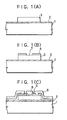
- Fig. 1 schematically illustrates a process for fabricating a planar-type TFT according to an exemplary embodiment of the present invention.
- a soda-lime glass substrate 1 On the surface of a soda-lime glass substrate 1 there was deposited a 300 nm thick silicon oxide film serving as a base protective film 2, the film 2 being deposited by a well known sputtering method.
- the film deposition was carried out under the following conditions: Sputter gas 100% O 2 Reaction pressure 0.5 Pa RF power 400 W Temperature of the substrate 150°C Rate of film deposition 5 nm/min.
- the film 3 was annealed by irradiation with excimer laser energy so as to crystallize the film 3 into a polycrystal.
- the conditions of the annealing process were as follows: Laser energy density 200 mJ/cm 2 Pulse repetition 50 shots.
- n-type non-single crystal silicon film doped with phosphorus such film serving as a low-resistance non-single crystal semiconductor layer.
- the deposition of this film was carried out by plasma chemical vapor deposition under the following conditions: Gas materials SiH 4 + PH 3 + H 2 Reaction pressure 0.05 Torr Temperature of the substrate 300°C RF power (13.56 MHz) 200 W Film thickness 50 nm.
- a microcrystalline film with a low electric resistance may be deposited as the n-type non-single crystal silicon film, by incorporating a large amount of H 2 gas into the gas materials at elevated RF power.
- the n-type non-single crystal semiconductor material of the source and the drain regions 4 was activated by irradiating the same with an excimer laser beam under the following conditions: Laser energy density 100 mJ/cm 2 Pulse repetition 50 shots.
- the channel portion 7 was then activated by plasma treatment in hydrogen under the following conditions: Temperature of the substrate 250°C RF power 100 W Duration of the treatment 60 minutes.
- the formation of the gate oxide film was carried out using the same materials and method as those used in the deposition of the base protective film 2.
- the etching of the contact holes was carried out by a method well known in the art.
- the conductivity of the source and drain n-type non-single crystal semiconductor material 4 changes as a function of the energy density of the irradiating excimer laser beam in the manner shown in Fig. 3.
- the conductivity of the semiconductor 4 increases with increasing energy density up to 150 mJ/cm 2 .
- the conductivity can be seen to decrease with further increase of the energy density since the N + layer surfaces of the source and drain are damaged by high energy laser irradiation. With still further increase of the energy density, the source and drain semiconductors 4 would sublime.
- the laser irradiation should be effected at an energy density preferably of 150 mJ/cm 2 or less, and more preferably in the range of from 100 mJ/cm 2 to 150 mJ/cm 2 .
- an energy density preferably of 150 mJ/cm 2 or less, and more preferably in the range of from 100 mJ/cm 2 to 150 mJ/cm 2 .
- the channel portion Since the channel portion was well crystallized by the laser annealing of the I-type semiconductor film 3, the channel portion would be degraded by the laser irradiation of the source and drain semiconductors 4 at an energy density of more than 150 mJ/cm 2 if the channel portion were not masked.
- the degradation is caused by stress which is, in turn, caused by the difference between the temperature of the channel portion and that of the other portions of the film 3 during the laser irradiation of the source and drain.
- this laser irradiation can be applied without degrading the channel portion if a not so high energy density of 150 mJ/cm 2 or less is applied.
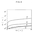
- Fig. 4 there is shown the change in the I D -V D characteristics of the TFT as a function of the energy density of the laser beam irradiation at zero gate potential.
- the abscissa represents the source-to-drain voltage, and the ordinate the source-to-drain current;
- curve 40 shows the I D -V D characteristics for a case without laser beam irradiation of the source and drain semiconductors, and
- curves 41 to 43 show the I D -V D characteristics for the cases in which source and drain semiconductors were irradiated with a laser beam at an energy of 100 mJ/cm 2 , 150 mJ/cm 2 , and 200 mJ/cm 2 , respectively.
- the gate insulating film 5 was formed after activation of the n-type source and drain semiconductors 4. In a practical process, however, the order may be reversed.
- a predetermined pattern etching thereof may be performed thereafter, followed by the activation of the source and the drain areas.
- the presence of the gate insulating film 5 on the I-type semiconductor film 3 may provide further favourable electric properties to the device since the presence thereof prevents degradation of the channel portion caused by laser irradiation.
- the process according to the present invention enables fabrication of a highly reliable TFT in a low temperature process.
- the TFT device moreover is of high performance, is furnished with a source and a drain having high electric conductivity, and is less influenced by parasitic resistances.
- an excimer laser beam can heat only the surface of a device irradiated therewith. Therefore, the substrate of the device is not subject to thermal damage and also a high density multilayered device can be made by the use of an excimer laser beam.
- the process according to the present invention is further advantageous in that the conventional heat treatment at high temperature is omitted.
- the process restrains impurities present in the substrate from penetrating into the active layers. This realizes TFTs having long term stability as regards their electric properties.
- a gate insulating film 5 and a base protective film 2 were provided under the source and the drain contacts 6. Since the same material and the same formation method were used for the films 2 and 5, there is little difference between the coefficients of thermal expansion of the films 2 and 5. Therefore, there is little difference between the thermal expansion of the film 2 and that of the film 5 caused by heat generated during operation of the TFT or by thermal treatments during the fabrication process. Accordingly, there is little risk that a metal electrode, such as an aluminum electrode or the like, provided on the uppermost surface of the device will peel off and become disconnected. Thus, it can be seen that the process according to the present invention provides TFTs which can function for a long period of time with high reliability.
- a silicon oxide film is used as a gate insulating film (gate oxide film), however, a silicon nitride layer or a multi-layer of silicon oxide and silicon nitride may be used as the gate insulating film instead.
- An I-type non-single crystal semiconductor film may be an intrinsic semiconductor film or a substantially intrinsic semiconductor film.
- a substantially intrinsic semiconductor film contains impurities at a concentration less than that of the source and drain n-type semiconductors.
- An irradiation beam for example a light beam or a YAG laser beam or the like, may be used for crystallizing the I-type non-single crystal semiconductor film instead of an excimer laser beam.
- An irradiation beam for example a light beam or a YAG laser beam or the like, may be used for activating the source and drain n-type semiconductors instead of an excimer laser beam.
- the light beam may for example be emitted from a halogen lamp or a Xe lamp.
Landscapes
- Thin Film Transistor (AREA)
- Recrystallisation Techniques (AREA)
Claims (11)
- Verfahren zur Herstellung eines Dünnschichttransistors, bei demauf einem Substrat (1) eine Halbleiterschicht aus einem Nicht-Einkristall gebildet wird,die Halbleiterschicht (3) aus Nicht-Einkristall mittels Bestrahlung mit einem ersten Strahl kristallisiert wird undauf die Halbleiterschicht (3) aus Nicht-Einkristall Source- und Drain-Halbleiterschichten (4) gebildet werden,dadurch gekennzeichnet, daß
die Source- und Drain-Halbleiterschichten (4) mittels Bestrahlung mit einem zweiten Strahl einer geringeren Energiedichte als der erste Strahl aktiviert werden. - Verfahren nach Anspruch 1, dadurch gekennzeichnet, daß die Energiedichte des zweiten Strahls 150 mJ/cm2 oder weniger beträgt.
- Verfahren nach einem der vorhergehenden Ansprüche, dadurch gekennzeichnet, daß die Source- und Drain-Halbleiterschichten (4) durch Ausbildung einer Halbleiterschicht mittels Chemical Vapor Deposition und durch Strukturierung der Halbleiterschicht zu Source- und Drain-Halbleiterschichten (4) gebildet werden.
- Verfahren nach einem der vorhergehenden Ansprüche, dadurch gekennzeichnet, daß die Halbleiterschicht (3) aus Nicht-Einkristall einen Eigenhalbleiter oder einen im wesentlichen eigenleitenden Halbleiter umfaßt.
- Verfahren nach einem der vorhergehenden Ansprüche, dadurch gekennzeichnet, daß bei der Bildung der Source- und Drain-Halbleiterschichten (4) ein Kanalbereich in der Halbleiterschicht (3) aus Nicht-Einkristall gebildet wird.
- Verfahren nach Anspruch 5, dadurch gekennzeichnet, daß die Bestrahlung der Source- und Drain-Schichten (4) ohne Maskierung des Kanalbereichs vorgenommen wird.
- Verfahren nach Anspruch 5, bei demauf den Kanalbereich und auf die Source- und Drain-Schichten (4) eine dünne Isolationsschicht (5) aufgebracht wird,Bereiche der dünnen Isolationsschicht (5) zur Bildung von durch die dünne Isolationsschicht (5) hindurch reichenden Kontaktöffnungen auf den Source- und Drain-Schichten (4) abgetragen werden, und bei dembei der Aktivierung der Source- und Drain-Schichten (4) diese sowie die verbleibenden Bereiche der dünnen Isolationsschicht (5) bestrahlt werden, wobei die verbleibenden Bereiche als Maske dienen.
- Verfahren nach Anspruch 7, dadurch gekennzeichnet, daß die dünne Isolationsschicht (5) Siliziumoxid, Siliziumnitrid oder eine Mehrfachschicht aus Siliziumoxid und Siliziumnitrid umfaßt.
- Verfahren nach Anspruch 7 oder 8, dadurch gekennzeichnet, daß eine obere Oberfläche des Kanalbereichs vollständig durch die verbleibenden Bereiche bedeckt ist.
- Verfahren nach einem der vorhergehenden Ansprüche, dadurch gekennzeichnet, daß die Source- und Drain-Schichten halbleitendes Material vom n-Leitfähigkeitstyp umfassen.
- Verfahren nach einem der vorhergehenden Ansprüche, dadurch gekennzeichnet, daß die Bestrahlung durch Verwendung eines Laserstrahls und/oder eines Lichtstrahls vorgenommen wird.
Applications Claiming Priority (2)
| Application Number | Priority Date | Filing Date | Title |
|---|---|---|---|
| JP2145069A JP2700277B2 (ja) | 1990-06-01 | 1990-06-01 | 薄膜トランジスタの作製方法 |
| JP145069/90 | 1990-06-01 |
Publications (3)
| Publication Number | Publication Date |
|---|---|
| EP0459836A2 EP0459836A2 (de) | 1991-12-04 |
| EP0459836A3 EP0459836A3 (en) | 1993-02-24 |
| EP0459836B1 true EP0459836B1 (de) | 1997-09-17 |
Family
ID=15376664
Family Applications (1)
| Application Number | Title | Priority Date | Filing Date |
|---|---|---|---|
| EP91305013A Expired - Lifetime EP0459836B1 (de) | 1990-06-01 | 1991-06-03 | Verfahren zum Herstellen von Dünnfilmtransistoren |
Country Status (5)
| Country | Link |
|---|---|
| US (3) | US6458200B1 (de) |
| EP (1) | EP0459836B1 (de) |
| JP (1) | JP2700277B2 (de) |
| KR (1) | KR950007355B1 (de) |
| DE (1) | DE69127656T2 (de) |
Cited By (2)
| Publication number | Priority date | Publication date | Assignee | Title |
|---|---|---|---|---|
| US6872605B2 (en) | 1992-12-04 | 2005-03-29 | Semiconductor Energy Laboratory Co., Ltd. | Semiconductor device and method of fabricating the same |
| US7045399B2 (en) | 1992-12-09 | 2006-05-16 | Semiconductor Energy Laboratory Co., Ltd. | Electronic circuit |
Families Citing this family (13)
| Publication number | Priority date | Publication date | Assignee | Title |
|---|---|---|---|---|
| JP2700277B2 (ja) * | 1990-06-01 | 1998-01-19 | 株式会社半導体エネルギー研究所 | 薄膜トランジスタの作製方法 |
| US5930608A (en) | 1992-02-21 | 1999-07-27 | Semiconductor Energy Laboratory Co., Ltd. | Method of fabricating a thin film transistor in which the channel region of the transistor consists of two portions of differing crystallinity |
| JPH06124913A (ja) | 1992-06-26 | 1994-05-06 | Semiconductor Energy Lab Co Ltd | レーザー処理方法 |
| CN100359633C (zh) * | 1992-12-09 | 2008-01-02 | 株式会社半导体能源研究所 | 制造半导体器件的方法 |
| TW425637B (en) * | 1993-01-18 | 2001-03-11 | Semiconductor Energy Lab | Method of fabricating mis semiconductor device |
| JP3173926B2 (ja) | 1993-08-12 | 2001-06-04 | 株式会社半導体エネルギー研究所 | 薄膜状絶縁ゲイト型半導体装置の作製方法及びその半導体装置 |
| US6331717B1 (en) | 1993-08-12 | 2001-12-18 | Semiconductor Energy Laboratory Co. Ltd. | Insulated gate semiconductor device and process for fabricating the same |
| US5681760A (en) * | 1995-01-03 | 1997-10-28 | Goldstar Electron Co., Ltd. | Method for manufacturing thin film transistor |
| JP3778456B2 (ja) | 1995-02-21 | 2006-05-24 | 株式会社半導体エネルギー研究所 | 絶縁ゲイト型薄膜半導体装置の作製方法 |
| JP3917205B2 (ja) * | 1995-11-30 | 2007-05-23 | 株式会社半導体エネルギー研究所 | 半導体装置の作製方法 |
| US6872607B2 (en) | 2000-03-21 | 2005-03-29 | Semiconductor Energy Laboratory Co., Ltd. | Method of manufacturing a semiconductor device |
| US7291522B2 (en) * | 2004-10-28 | 2007-11-06 | Hewlett-Packard Development Company, L.P. | Semiconductor devices and methods of making |
| JP6003321B2 (ja) * | 2012-07-18 | 2016-10-05 | Jfeスチール株式会社 | 方向性電磁鋼板の製造方法 |
Citations (2)
| Publication number | Priority date | Publication date | Assignee | Title |
|---|---|---|---|---|
| EP0301463A2 (de) * | 1987-07-27 | 1989-02-01 | Nippon Telegraph And Telephone Corporation | Dünnschicht-Siliciumhalbleiteranordnung und Verfahren zu ihrer Herstellung |
| EP0331811A2 (de) * | 1987-12-18 | 1989-09-13 | Fujitsu Limited | Halbleiteranordnungen mit Silicium-auf-Isolator(SOI)-Strukturen |
Family Cites Families (27)
| Publication number | Priority date | Publication date | Assignee | Title |
|---|---|---|---|---|
| US4174217A (en) * | 1974-08-02 | 1979-11-13 | Rca Corporation | Method for making semiconductor structure |
| JPS558026A (en) | 1978-06-30 | 1980-01-21 | Matsushita Electric Ind Co Ltd | Semi-conductor device manufacturing method |
| EP0171509B1 (de) * | 1979-07-24 | 1990-10-31 | Hughes Aircraft Company | Verfahren zur Laserbehandlung für "Silizium auf Saphir" |
| US4266986A (en) * | 1979-11-29 | 1981-05-12 | Bell Telephone Laboratories, Incorporated | Passivation of defects in laser annealed semiconductors |
| JPS5785262A (en) * | 1980-11-17 | 1982-05-27 | Toshiba Corp | Manufacture of metal oxide semiconductor type semiconductor device |
| JPS5814524A (ja) * | 1981-07-17 | 1983-01-27 | Fujitsu Ltd | 半導体装置の製造方法 |
| JPS58164267A (ja) | 1982-03-25 | 1983-09-29 | Seiko Epson Corp | 薄膜シリコントランジスタの製造方法 |
| US4769338A (en) * | 1984-05-14 | 1988-09-06 | Energy Conversion Devices, Inc. | Thin film field effect transistor and method of making same |
| US4727044A (en) * | 1984-05-18 | 1988-02-23 | Semiconductor Energy Laboratory Co., Ltd. | Method of making a thin film transistor with laser recrystallized source and drain |
| JPS61135110A (ja) * | 1984-12-05 | 1986-06-23 | Fujitsu Ltd | 半導体装置の製造方法 |
| DE3689735T2 (de) * | 1985-08-02 | 1994-06-30 | Semiconductor Energy Lab | Verfahren und Gerät zur Herstellung von Halbleitervorrichtungen. |
| US4933296A (en) * | 1985-08-02 | 1990-06-12 | General Electric Company | N+ amorphous silicon thin film transistors for matrix addressed liquid crystal displays |
| JPH07120802B2 (ja) * | 1985-08-08 | 1995-12-20 | ソニー株式会社 | 半導体装置の製造方法 |
| JPS6239067A (ja) | 1985-08-13 | 1987-02-20 | Seiko Instr & Electronics Ltd | 薄膜半導体装置の製造方法 |
| JPH0746729B2 (ja) * | 1985-12-26 | 1995-05-17 | キヤノン株式会社 | 薄膜トランジスタの製造方法 |
| JPS62254467A (ja) * | 1986-04-28 | 1987-11-06 | Seiko Instr & Electronics Ltd | 薄膜トランジスタの製造方法 |
| JPS63200572A (ja) | 1987-02-17 | 1988-08-18 | Seiko Instr & Electronics Ltd | 薄膜半導体装置の製造方法 |
| JPS63250178A (ja) | 1987-04-07 | 1988-10-18 | Seiko Instr & Electronics Ltd | 薄膜半導体装置の製造方法 |
| JPS63292682A (ja) * | 1987-05-26 | 1988-11-29 | Seiko Instr & Electronics Ltd | 薄膜半導体装置の製造方法 |
| US4743567A (en) * | 1987-08-11 | 1988-05-10 | North American Philips Corp. | Method of forming thin, defect-free, monocrystalline layers of semiconductor materials on insulators |
| JPH02130912A (ja) | 1988-11-11 | 1990-05-18 | Seiko Epson Corp | 薄膜半導体装置 |
| JP2867264B2 (ja) * | 1989-02-28 | 1999-03-08 | 株式会社日立製作所 | 液晶表示装置およびその製造方法 |
| JP2832991B2 (ja) * | 1989-04-14 | 1998-12-09 | ソニー株式会社 | 多層配線形成方法および連続処理装置 |
| JP2700277B2 (ja) * | 1990-06-01 | 1998-01-19 | 株式会社半導体エネルギー研究所 | 薄膜トランジスタの作製方法 |
| US5162239A (en) * | 1990-12-27 | 1992-11-10 | Xerox Corporation | Laser crystallized cladding layers for improved amorphous silicon light-emitting diodes and radiation sensors |
| GB9114018D0 (en) * | 1991-06-28 | 1991-08-14 | Philips Electronic Associated | Thin-film transistor manufacture |
| US5424244A (en) * | 1992-03-26 | 1995-06-13 | Semiconductor Energy Laboratory Co., Ltd. | Process for laser processing and apparatus for use in the same |
-
1990
- 1990-06-01 JP JP2145069A patent/JP2700277B2/ja not_active Expired - Lifetime
-
1991
- 1991-06-01 KR KR1019910009163A patent/KR950007355B1/ko not_active Expired - Lifetime
- 1991-06-03 EP EP91305013A patent/EP0459836B1/de not_active Expired - Lifetime
- 1991-06-03 DE DE69127656T patent/DE69127656T2/de not_active Expired - Lifetime
-
1993
- 1993-07-12 US US08/089,650 patent/US6458200B1/en not_active Expired - Lifetime
-
2002
- 2002-02-21 US US10/078,354 patent/US6740547B2/en not_active Expired - Fee Related
-
2004
- 2004-05-25 US US10/852,700 patent/US7018874B2/en not_active Expired - Fee Related
Patent Citations (2)
| Publication number | Priority date | Publication date | Assignee | Title |
|---|---|---|---|---|
| EP0301463A2 (de) * | 1987-07-27 | 1989-02-01 | Nippon Telegraph And Telephone Corporation | Dünnschicht-Siliciumhalbleiteranordnung und Verfahren zu ihrer Herstellung |
| EP0331811A2 (de) * | 1987-12-18 | 1989-09-13 | Fujitsu Limited | Halbleiteranordnungen mit Silicium-auf-Isolator(SOI)-Strukturen |
Non-Patent Citations (1)
| Title |
|---|
| Laser annealing of semiconductors, Ed. J.M. Poate et al, Academic Press, 1982 * |
Cited By (8)
| Publication number | Priority date | Publication date | Assignee | Title |
|---|---|---|---|---|
| US6872605B2 (en) | 1992-12-04 | 2005-03-29 | Semiconductor Energy Laboratory Co., Ltd. | Semiconductor device and method of fabricating the same |
| US7045399B2 (en) | 1992-12-09 | 2006-05-16 | Semiconductor Energy Laboratory Co., Ltd. | Electronic circuit |
| US7061016B2 (en) | 1992-12-09 | 2006-06-13 | Semiconductor Energy Laboratory Co., Ltd. | Electronic circuit |
| US7105898B2 (en) | 1992-12-09 | 2006-09-12 | Semiconductor Energy Laboratory Co., Ltd. | Electronic circuit |
| US7547916B2 (en) | 1992-12-09 | 2009-06-16 | Semiconductor Energy Laboratory Co., Ltd. | Electronic circuit |
| US7897972B2 (en) | 1992-12-09 | 2011-03-01 | Semiconductor Energy Laboratory Co., Ltd. | Electronic circuit |
| US8294152B2 (en) | 1992-12-09 | 2012-10-23 | Semiconductor Energy Laboratory Co., Ltd. | Electronic circuit including pixel electrode comprising conductive film |
| US7238558B2 (en) | 1993-06-30 | 2007-07-03 | Semiconductor Energy Laboratory Co., Ltd. | Semiconductor device and method of fabricating the same |
Also Published As
| Publication number | Publication date |
|---|---|
| US20050009254A1 (en) | 2005-01-13 |
| EP0459836A3 (en) | 1993-02-24 |
| US6740547B2 (en) | 2004-05-25 |
| US6458200B1 (en) | 2002-10-01 |
| DE69127656D1 (de) | 1997-10-23 |
| US20030017656A1 (en) | 2003-01-23 |
| JP2700277B2 (ja) | 1998-01-19 |
| JPH0437144A (ja) | 1992-02-07 |
| DE69127656T2 (de) | 1998-04-30 |
| EP0459836A2 (de) | 1991-12-04 |
| KR950007355B1 (ko) | 1995-07-10 |
| US7018874B2 (en) | 2006-03-28 |
Similar Documents
| Publication | Publication Date | Title |
|---|---|---|
| KR100333153B1 (ko) | 반도체장치제작방법 | |
| JP3193803B2 (ja) | 半導体素子の作製方法 | |
| US5858823A (en) | Semiconductor circuit for electro-optical device and method of manufacturing the same | |
| US7056775B2 (en) | Semiconductor device and process for fabricating the same | |
| US5851860A (en) | Semiconductor device and method for producing the same | |
| US5930608A (en) | Method of fabricating a thin film transistor in which the channel region of the transistor consists of two portions of differing crystallinity | |
| KR100280171B1 (ko) | 비단결정반도체장치(박막트랜지스터)와 이것을 이용한 액정표시장치 및 그 제조방법 | |
| US5834071A (en) | Method for forming a thin film transistor | |
| JPH0758339A (ja) | 半導体装置およびその作製方法 | |
| US6458200B1 (en) | Method for fabricating thin-film transistor | |
| JP2001028448A (ja) | 薄膜トランジスタの作製方法 | |
| KR20030069779A (ko) | 박막트랜지스터 및 그 제조방법 | |
| KR100700681B1 (ko) | 반도체박막의 결정화 방법 및 박막 반도체장치의 제조방법 | |
| JPH07131034A (ja) | 半導体装置の作製方法 | |
| JP3347340B2 (ja) | 薄膜トランジスタの製造方法 | |
| JPH04340725A (ja) | 薄膜トランジスタの製造方法 | |
| JPH0832074A (ja) | 半導体装置およびその製造方法 | |
| JP3380527B2 (ja) | 半導体装置の作製方法 | |
| JPH0982639A (ja) | 半導体装置およびその製造方法 | |
| JP3181901B2 (ja) | 薄膜トランジスタ | |
| JP2852855B2 (ja) | 半導体装置の作製方法 | |
| EP0955674B1 (de) | Herstellung von hybriden polykristallinen und amorphen Siliziumstrukturen | |
| JP3181817B2 (ja) | 薄膜トランジスタ | |
| JPH0831737A (ja) | 半導体装置およびその製造方法 | |
| JP2789417B2 (ja) | 半導体装置の作製方法 |
Legal Events
| Date | Code | Title | Description |
|---|---|---|---|
| PUAI | Public reference made under article 153(3) epc to a published international application that has entered the european phase |
Free format text: ORIGINAL CODE: 0009012 |
|
| AK | Designated contracting states |
Kind code of ref document: A2 Designated state(s): DE FR GB |
|
| PUAL | Search report despatched |
Free format text: ORIGINAL CODE: 0009013 |
|
| AK | Designated contracting states |
Kind code of ref document: A3 Designated state(s): DE FR GB |
|
| 17P | Request for examination filed |
Effective date: 19930625 |
|
| 17Q | First examination report despatched |
Effective date: 19941024 |
|
| GRAG | Despatch of communication of intention to grant |
Free format text: ORIGINAL CODE: EPIDOS AGRA |
|
| GRAH | Despatch of communication of intention to grant a patent |
Free format text: ORIGINAL CODE: EPIDOS IGRA |
|
| GRAH | Despatch of communication of intention to grant a patent |
Free format text: ORIGINAL CODE: EPIDOS IGRA |
|
| GRAA | (expected) grant |
Free format text: ORIGINAL CODE: 0009210 |
|
| AK | Designated contracting states |
Kind code of ref document: B1 Designated state(s): DE FR GB |
|
| REF | Corresponds to: |
Ref document number: 69127656 Country of ref document: DE Date of ref document: 19971023 |
|
| ET | Fr: translation filed | ||
| PLBE | No opposition filed within time limit |
Free format text: ORIGINAL CODE: 0009261 |
|
| STAA | Information on the status of an ep patent application or granted ep patent |
Free format text: STATUS: NO OPPOSITION FILED WITHIN TIME LIMIT |
|
| 26N | No opposition filed | ||
| REG | Reference to a national code |
Ref country code: GB Ref legal event code: IF02 |
|
| PGFP | Annual fee paid to national office [announced via postgrant information from national office to epo] |
Ref country code: FR Payment date: 20100709 Year of fee payment: 20 |
|
| PGFP | Annual fee paid to national office [announced via postgrant information from national office to epo] |
Ref country code: GB Payment date: 20100602 Year of fee payment: 20 Ref country code: DE Payment date: 20100526 Year of fee payment: 20 |
|
| REG | Reference to a national code |
Ref country code: DE Ref legal event code: R071 Ref document number: 69127656 Country of ref document: DE |
|
| REG | Reference to a national code |
Ref country code: DE Ref legal event code: R071 Ref document number: 69127656 Country of ref document: DE |
|
| REG | Reference to a national code |
Ref country code: GB Ref legal event code: PE20 Expiry date: 20110602 |
|
| PG25 | Lapsed in a contracting state [announced via postgrant information from national office to epo] |
Ref country code: GB Free format text: LAPSE BECAUSE OF EXPIRATION OF PROTECTION Effective date: 20110602 |
|
| PG25 | Lapsed in a contracting state [announced via postgrant information from national office to epo] |
Ref country code: DE Free format text: LAPSE BECAUSE OF EXPIRATION OF PROTECTION Effective date: 20110604 |