EP0464632A2 - Système de traitement de données parallèles avec un signal de compensation de décalage - Google Patents
Système de traitement de données parallèles avec un signal de compensation de décalage Download PDFInfo
- Publication number
- EP0464632A2 EP0464632A2 EP91110561A EP91110561A EP0464632A2 EP 0464632 A2 EP0464632 A2 EP 0464632A2 EP 91110561 A EP91110561 A EP 91110561A EP 91110561 A EP91110561 A EP 91110561A EP 0464632 A2 EP0464632 A2 EP 0464632A2
- Authority
- EP
- European Patent Office
- Prior art keywords
- signal
- pairs
- delay
- path
- signal paths
- Prior art date
- Legal status (The legal status is an assumption and is not a legal conclusion. Google has not performed a legal analysis and makes no representation as to the accuracy of the status listed.)
- Granted
Links
Images













Classifications
-
- G—PHYSICS
- G06—COMPUTING OR CALCULATING; COUNTING
- G06F—ELECTRIC DIGITAL DATA PROCESSING
- G06F1/00—Details not covered by groups G06F3/00 - G06F13/00 and G06F21/00
- G06F1/04—Generating or distributing clock signals or signals derived directly therefrom
- G06F1/10—Distribution of clock signals, e.g. skew
Definitions
- the present invention relates to a parallel data processing apparatus which comprises a plurality of processors which are operated in parallel in synchronization with a common clock, and the operations of which are started upon receiving a common asynchronous request signal.
- the present invention can be applied to a single instruction stream multiple data stream (SIMD) type parallel data processing apparatus.
- SIMD single instruction stream multiple data stream
- the above asynchronous request signal may be an interrupt signal output from a host processor to the processors in the parallel data processing apparatus, and the above asynchronous request signal must be received (latched) at the same time to ensure a synchronous parallel operation of all of the processors.
- the lengths of signal lines for each of the asynchronous request signal and the clock signal from the output point thereof to the plurality of processors are designed to be same (equal-length wiring), so that the asynchronous request signal is received simultaneously in each of the plurality of processors.
- the above equal-length wiring imposes a very severe design requirement on the designer of the parallel data processing apparatus. Further, a high accuracy of the timing of the operations of the plurality of processors cannot be achieved by the equal-length wiring, and therefore, the frequency of the clock signal cannot be increased in a parallel data processing apparatus designed to use the equal-length wiring.
- An object of the present invention is to provide a parallel data processing apparatus comprising a plurality of processors which are operated in parallel in synchronization with a common clock, and the operations of which are started upon receiving a common asynchronous request signal, where severe design requirements for equal-length wiring are reduced or eliminated, a high accuracy of the timing of the operations of the plurality of processors can be obtained, and a high frequency clock signal can be used.
- an apparatus for supplying a signal to a plurality of data processing units comprising: a plurality of pairs of signal paths, these pairs respectively corresponding to the plurality of data processing units, one signal path of each of the plurality of pairs being provided for supplying the signal from a predetermined position common to all of the plurality of pairs of signal paths, to a corresponding data processing unit, the other signal path of each of the plurality of pairs being provided for returning the signal from the corresponding data processing unit to the predetermined position, and the signal paths in each of the plurality of pairs are made symmetrical with regard to an electrical length for signal propagation, where each of the plurality of pairs of signal paths comprises a variable delay unit for delaying a propagation of a signal through the signal path; a delay measuring unit for measuring a time elapsing while the signal is propagated from the predetermined position to the corresponding data processing unit and then returned from the processor to the predetermined position through each pair of signal paths; and a delay adjusting unit for
- a parallel data processing apparatus comprising: a plurality of processors for processing data in parallel, in synchronization with a common clock signal, and the operations of which are started upon receiving a common asynchronous request signal; a clock generating unit for generating the common clock signal to the plurality of processors; a plurality of pairs of signal paths, the pairs respectively corresponding to the plurality of processors, one signal path of each of the plurality of pairs is provided for supplying the predetermined one of the clock signal and the asynchronous request signal from a predetermined position which is common to all of the plurality of pairs of signal paths, to a corresponding processor, the other signal path of each of the plurality of pairs is provided for returning the predetermined one of the clock signal and the asynchronous request signal from the corresponding processor to the predetermined position, and the signal paths in each of the plurality of pairs are made symmetrical with regard to the electrical length for a signal propagation, where each of the plurality of pairs of signal paths comprises a variable delay
- a parallel data processing apparatus comprising: a plurality of processors for processing data in parallel, in synchronization with a common clock signal, and the operations of which is started upon receiving a common asynchronous request signal; a clock generating unit for generating the common clock signal to the plurality of processors; a first plurality of pairs of signal paths, the pairs respectively corresponding to the plurality of processors, one signal path of each of the first plurality of pairs is provided for supplying the clock signal from a first predetermined position common to all of the first plurality of pairs of signal paths, to a corresponding processor, the other signal path of each of the first plurality of pairs is provided for returning the clock signal from the corresponding processor to the first predetermined position, and the signal paths in each of the first plurality of pairs are made symmetrical with regard to the electrical length for a signal propagation, where each of the first plurality of pairs of signal paths comprises a first variable delay unit for delaying a propagation of a clock signal through the signal path
- the time which elapses while the signal propagates from the predetermined position to the corresponding data processing unit and then returns from the processor to the predetermined position through each pair of signal paths, is measured by the delay measuring unit.
- This can be realized by the provision of the plurality of pairs of signal paths where the pairs respectively corresponding to the plurality of data processing units, and the signal paths in each of the plurality of pairs are made symmetrical with regard to the electrical length for a signal propagation.
- the delays caused by the variable delay unit in all of the signal paths of the plurality of pairs of signal paths are adjusted, based on results of measurement by the delay measuring unit so that times elapsing while the signal is propagated from the predetermined position to the plurality of data processing units through the respective signal paths of the plurality of pairs of signal paths for supplying the signal to the data processing units, are equal.
- the above provision of the first aspect of the present invention is made for a predetermined one of the clock signal and the asynchronous request signal.
- the above provision of the first aspect of the present invention is made for both the clock signal and the asynchronous request signal.
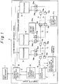
- Figure 1 is a block diagram showing a construction of the first embodiment of the present invention.
- reference numeral 1 denotes a host processor
- 2 denotes a parallel data processing apparatus
- 31, 32 ... 3 n each denote a processor
- 4 denotes a clock generator
- 5 denotes a request reception circuit
- 6a1, 6a2, ... 6a n each denote a programmable delay circuit
- 7a denotes a delay time measuring & setting circuit
- 9a1, 9a2, ... 9a n each denote a selector
- 10a1, 10a2, ... 10a n each denote a programmable delay circuit, 11a1, 11a2, ...
- 11a n each denote a selector
- 12a2 denotes an offset adjusting circuit
- 13a and 13a' each denote a waveform shaping circuit
- 14a denotes an offset adjusting circuit
- 15 denotes a clock signal supply path
- 16 denotes a return path corresponding to the clock signal supply path
- 17 denotes an asynchronous request signal path
- 18 denotes an acknowledge signal path
- 33a1, 33a2, ... 33a n each denote a branch path for supplying a clock signal to each processor
- 34a1, 34a2, ... 34a n each denote a branch path for returning the clock signal from a corresponding processor to the return path 16.
- Fig. 1 The construction of Fig. 1 is an embodiment of the above-mentioned second aspect of the present invention.
- the clock signal supply path 15 and the return path 16 are provided along the plurality of processors 31, 32, ... 3 n .
- One end of each of the clock signal supply path 15 and the return path 16 is connected with the clock generator 4.
- all other designs in the clock signal supply path 15 and the corresponding return path 16 are made symmetrical with regard to a signal propagation.
- the clock signal supply path 15 has a branch path 33a1, 33a2, ... 33a n for each of the plurality of processors 31, 32, ... 3 n , where each branch path 33a1, 33a2, ...
- the return path 16 has a branch path 34a1, 34a2, ... 34a n for each of the plurality of processors 31, 32, ... 3 n , where each branch path 34a1, 34a2, ... 34a n is provided corresponding to one of the above branch paths 33a1, 33a2, ... 33a n , and connects the return path 16 with the clock input terminal of the corresponding processor. All other designs in the above corresponding branch paths 33a1, 33a2, ... 33a n and 34a1, 34a2, ... 34a n are made symmetrical with regard to a signal propagation.
- One of the programmable delay circuits (variable delay circuits) 6a1, 6a2, ... 6a n is provided on a corresponding one of the branch paths 33a1, 33a2, ... 33a n
- one of the programmable delay circuits (variable delay circuits) 10a1, 10a2, ... 10a n is provided on a corresponding one of the branch paths 34a1, 34a2, ... 34a n
- the return path 16 comprises thereon the plurality of selectors 9a1, 9a2, ... 9a n .
- Each of the selectors 9a1, 9a2, ... 9a n-1 connects at its two input terminals the upstream side of the return path 16 and a corresponding one of the branch paths 10a1, 10a2, ...
- the selectors 11a1, 11a2, ... 11a n are provided on the clock signal supply path 15 at the locations corresponding to the locations of the selectors 9a1, 9a2, ... 9a n on the return path 16.
- Each of the clock signal supply path 15 and the return path 16 comprises a waveform shaping circuit 13a or 13a' for maintaining the waveform of the clock signal.
- the waveform shaping circuits 13a and 13a' on the clock signal supply path 15 and the return path 16 are provided in correspondence to each other.
- the offset adjusting circuit 14a is provided for the corresponding waveform shaping circuits 13a and 13a' to initially adjust the delay times caused by the corresponding waveform shaping circuits 13a and 13a' so that the initial delay times caused by the corresponding waveform shaping circuits 13a and 13a' are equal.
- the offset adjusting circuit 12a1, 12a2, ... 12a n may be provided for each pair of corresponding programmable delay circuits 6a1, 6a2, ...
- a common offset adjusting circuit may be provided for all pairs of the corresponding programmable delay circuits 6a1, 6a2, ... 6a n , and 10a1, 10a2, ... 10a n .
- An input terminal of the delay time measuring & setting circuit 7a is connected to the clock signal supply path 15 at the clock output terminal of the clock generator 4, and a clock output terminal of the delay time measuring & setting circuit 7a is connected to the return path 16 at the clock input terminal of the clock generator 4.
- the delay time measuring & setting circuit 7a measures a propagation delay time for a signal to be propagated from the delay time measuring & setting circuit 7a to the clock input terminal of each processor and then propagated from the clock input terminal of the processor to the delay time measuring & setting circuit 7a. Then, the delay time measuring & setting circuit 7a obtains a propagation delay time for a signal to be propagated from the delay time measuring & setting circuit 7a to the clock input terminal of each processor by dividing the above measured time by two, taking advantage of the above symmetricallity of the paths between the delay time measuring & setting circuit 7a and each processor. After obtaining the propagation delay times for all of the plurality of processors 31, 32, ...
- the delay time measuring & setting circuit 7a sets an additional delay time in the corresponding one of the programmable delay circuits 6a1, 6a2, ... 6a n on the corresponding one of the branch paths 33a1, 33a2, ... 33a n to each processor so that propagation delay times from the clock output terminal of the clock generator 4 to the input terminals of the plurality of processors 31, 32, ... 3 n , are the same.
- the above additional time for each programmable delay circuit can be determined as a difference between the maximum of the above obtained propagation delay times to the processors and the obtained propagation delay time to the corresponding processor, as shown in Fig. 2.
- an initial setting of the parallel data processing apparatus 2 of Fig. 1 is completed.
- the request reception circuit 5 receives an asynchronous request signal supplied from the host processor 1.
- the asynchronous request signal is, for example, an interrupt signal, or a hold request signal.
- the request reception circuit 5 sends a clock frequency down control signal to the clock generator 4 to temporarily lower the frequency of the clock signal output from the clock generator 4.
- the clock generator 4 comprises an oscillator, a frequency divider, and a frequency division rate control circuit for controlling a frequency division rate of the frequency divider.
- the frequency division rate control circuit temporarily lowers the frequency of the clock signal.
- the frequency division rate control circuit sends a complete signal, which indicates a completion of the lowering operation of the frequency of the clock signal, to the request reception circuit 5.
- the request reception circuit 5 Upon receiving the complete signal, the request reception circuit 5 sends the asynchronous request signal to the plurality of processors 31, 32, ... 3 n through the asynchronous request signal path 17.
- the processor returns an acknowledge signal to the request reception circuit 5 through the acknowledge signal path 18.
- the request reception circuit 5 When the request reception circuit 5 receives the acknowledge signal, the request reception circuit 5 sends a clock frequency up control signal to the clock generator 4.
- the frequency division rate control circuit Upon receiving the clock frequency up control signal, the frequency division rate control circuit temporarily increases the frequency of the clock signal to a predetermined frequency used in a normal operation. Namely, the above reception of the asynchronous request signal by each processor is carried out while the frequency of the clock signal supplied to the processor is lowered, i.e., the clock cycle is lengthened (for example, a normal cycle 30 nsec is increased to 240 nsec), and therefore, the operations in the respective processors 31, 32, ... 3 n responding to the asynchronous request signal can start within the same clock cycle even when the times at which the asynchronous request signal reaches the respective processors differ, as long as the difference in the times is within the lengthened clock cycle.
- the above asynchronous request signal path 17 to the plurality of processors 31, 32, ... 3 n may be designed by the conventional equal-length wiring. In this case, the above provision for lowering the frequency of the clock signal when receiving an asynchronous request signal may not be necessary.
- Figure 3 is a block diagram showing a construction of the second embodiment of the present invention.
- reference numeral 2' denotes a parallel data processing apparatus
- 5' denotes a request reception circuit
- 6b1, 6b2, ... 6b n each denote a programmable delay circuit
- 7b denotes a delay time measuring & setting circuit
- 9b1, 9b2, ... 9b n each denote a selector
- 10b1, 10b2, ... 10b n each denote a programmable delay circuit, 11b1, 11b2, ...
- 11b n each denote a selector
- 12b2 denotes an offset adjusting circuit
- 13b and 13b' each denote a waveform shaping circuit
- 14b denotes an offset adjusting circuit
- 15 denotes a clock signal supply path
- 16 denotes a clock signal return path
- 17 denotes an asynchronous request signal path
- 18 denotes an acknowledge signal path
- 19 denotes an asynchronous request signal path
- 20 denotes a return path corresponding to the asynchronous request signal path 19
- 21 denotes a clock signal supply path
- 33b1, 33b2, ... 33b n each denote a branch path for supplying a clock signal to each processor
- Fig. 3 is an embodiment of the above-mentioned second aspect of the present invention.
- a provision for adjusting propagation delay times to the plurality of processors 31, 32, ... 3 n is made for a construction for supplying the asynchronous request signal; conversely, the provision is made for the construction for supplying the clock signal in the construction of Fig. 1.
- the frequency of the clock signal is lowered when an asynchronous request signal is supplied to the plurality of processors 31, 32, ... 3 n .
- the control operations for lowering and increasing of the frequency of the clock signal are carried out by supplying the clock frequency down control signal and the clock frequency up control signal output from the request reception circuit 5' to the clock generator 4 responding to the reception of the asynchronous request signal from the host processor 1 and the reception of the acknowledge signal from the processors.
- the request reception circuit 5' outputs the asynchronous request signal to the plurality of processors 31, 32, ... 3 n when receiving the complete signal from the clock generator 4, respectively.
- the above reception of the asynchronous request signal by each processor is carried out while the frequency of the clock signal supplied to the processor is lowered, i.e., the clock cycle is lengthened, and therefore, the operations in the respective processors 31, 32, ... 3 n responding to the asynchronous request signal can start within the same clock cycle even when the times at which the clock signal reaches the respective processors differ, as long as the difference in the times is within the lengthened clock cycle.
- the above clock signal supply path 21 to the plurality of processors 31, 32, ... 3 n may be designed by the conventional equal-length wiring. In this case, the above provision for lowering the frequency of the clock signal when receiving an asynchronous request signal may not be necessary.
- Figure 4 is a block diagram showing a construction of the third embodiment of the present invention.
- reference numeral 2'' denotes a parallel data processing apparatus
- 5'' denotes a request reception circuit.
- the other elements in Fig. 4, which are denoted by the same reference numerals as Figs. 1 and 2, are respectively the same elements as shown in these figures.
- Fig. 4 is an embodiment of the above-mentioned third aspect of the present invention.
- the provision for adjusting propagation delay times to the plurality of processors 31, 32, ... 3 n is made for both the construction for supplying the asynchronous request signal and the construction for supplying the clock signal, where the respective provisions are the same as those shown in Figs. 1 and 3.
- FIG. 5 is a block diagram showing a construction of the fourth embodiment of the present invention.
- reference numeral 1' denotes a host processor
- 200 denotes a parallel data processing apparatus
- 221, 222, ... 22 n each denote a processor
- 23 denotes an MPU clock generator
- 24 denotes a request reception & clock control circuit
- 251, 252, ... 25 n each denote a delay & switch circuit
- 27 denotes a delay time measuring & setting circuit
- 28 denotes a control bus
- 29 denotes an asynchronous request signal path
- 30 denotes an acknowledge signal path
- 31 denotes a clock signal supply path
- 32 denotes a return path corresponding to the clock signal supply path 31.
- the delay & switch circuits 251, 252, ... 25 n are each provided for a corresponding one of the plurality of processors 221, 222, ... 22 n , and are chain connected to the delay time measuring & setting circuit 27.
- Fig. 5 is an embodiment of the above-mentioned second aspect of the present invention, and is basically similar to the construction of Fig. 1.
- the function for supplying the clock signal to the plurality of processors 221, 222, ... 22 n which is similar to the corresponding function in the construction of Fig. 1, is realized by the plurality of delay & switch circuits 251, 252, ... 25 n and the delay time measuring & setting circuit 27. Details of each of the delay & switch circuits 251, 252, ... 25 n and the delay time measuring & setting circuit 27 will be explained later.
- FIG. 6 is a block diagram showing a construction of the MPU clock generator 23 in the construction of Fig. 5.
- reference numeral 230 denotes a controller
- 231 denotes a frequency division rate counter
- 232 denotes a frequency divider.
- the controller 230 receives an up/down control signal supplied from the request reception & clock control circuit 24, and outputs an up/down signal U/D to the frequency division rate counter 231 according to the received up/down control signal.
- Figure 7 is a state transition diagram of the frequency division rate counter 231 in the construction of Fig. 6.
- the frequency division rate counter 231 is initially in the state "S7", where the frequency division rate counter 231 outputs a count equal to seven.
- FIG. 8 is a state transition diagram of the frequency divider 232 in the construction of Fig. 6.
- the frequency divider 232 is realized by a counter in which the count is increased by one when a leading edge of a master clock signal is supplied thereto from a master oscillator (not shown).
- the count of the counter is cyclically changed from 0 to i, and a carry signal is output when the count reaches i.
- the frequency divider 232 When the state of the frequency division rate counter 231 is "S0", the frequency divider 232 outputs an MPU clock signal having a frequency which is the same as the frequency of the master clock signal. Namely, the frequency division rate in the frequency divider 232 is equal to i+1.
- Figure 9 is a state transition diagram of the request reception & clock control circuit 24 in the construction of Fig. 5.
- the request reception & clock control circuit 24 is in an initial state "Init” after power is made ON.
- the timing of an example operation of the MPU clock generator 23 of Fig. 6 is shown in Fig. 10.
- a plurality of paths for supplying a plurality of asynchronous request signals to the processors and a plurality of paths for returning a plurality of acknowledge signals corresponding to the plurality of asynchronous request signals to the request reception & clock control circuit 24 are provided.
- the plurality of asynchronous request signals may include interrupt signals of a plurality of priority levels, and a hold request signal.
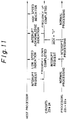
- Figure 11 is a diagram showing an example sequence in reception of an interrupt request signal by the parallel data processing apparatus 200 in Fig. 5.
- the request reception & clock control circuit 24 starts the above-mentioned operation for lowering the frequency of the MPU clock signal.
- the request reception & clock control circuit 24 outputs a LOW SPEED INDICATION to the host processor 1', and outputs an interrupt request signal to the plurality of processors 221, 222, ... 22 n .
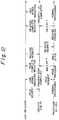
- Figure 12 is a diagram showing an example sequence in reception of a hold request signal by the parallel data processing apparatus 200 in Fig. 5.
- the request reception & clock control circuit 24 starts the above-mentioned operation for lowering the frequency of the MPU clock signal.
- the request reception & clock control circuit 24 outputs a LOW SPEED INDICATION to the host processor 1', and outputs a hold signal to the plurality of processors 221, 222, ... 22 n .
- the processors 221, 222, ... 22 n carry out a hold processing.
- the host processor 1' When receiving the HOLD COMPLETE INDICATION, the host processor 1' sends a release request signal to the request reception & clock control circuit 24, and the release request signal is transferred to the processors 221, 222, ... 22 n .
- the request reception & clock control circuit 24 starts the above-mentioned operation for increasing the frequency of the MPU clock signal to the frequency of the master clock signal, and when the operation is completed, the request reception & clock control circuit 24 sends a HIGH SPEED INDICATION to the host processor 1'.
- reference numerals 250, 252, 257, and 259 each denote a buffer amplifier
- 251, 254, 255, and 258 each denote a selector
- 253 and 256 each denote a programmable delay circuit.
- reference numerals A to G respectively correspond to the denotations of the terminals of Fig. 5.
- the MPU clock signal is supplied from the delay time measuring & setting circuit 27 or one of the delay & switch circuits 251, 252, ... 25 n to the delay & switch circuit of Fig. 13 through the input port C.
- the MPU clock signal passes through the buffer amplifier 250 and the selector 251.
- the selector 251 corresponds to one of the selectors 11a1, 11a2, ... 11a n in Fig. 1.
- the output of the selector 251 is divided into two ways: a way to another (if any) of the delay & switch circuits 251, 252, ...
- the output of the selector 254 is further divided into two ways: the above way to the other of the delay & switch circuits 251, 252, ... 25 n on the downstream side through the output port E; and a loop-back way toward the MPU clock generator 23.
- the loop-back way is connected with an input terminal of the selector 255.
- a timing signal output from the corresponding processor is applied to the other input terminal of the selector 255 through the input port B of the delay & switch circuit.
- the output of the selector 255 is applied to the programmable delay circuit 256, and the output of the programmable delay circuit 256 is applied to one of the input terminal of the selector 258.
- the output of the selector 258 is output through the buffer amplifier 259 and the output port D.
- the buffer amplifier 257 is provided corresponding to the buffer amplifier 252; the selector 255 is provided corresponding to the selector 254; the programmable delay circuit 256 is provided corresponding to the programmable delay circuit 253; the selector 258 is provided corresponding to the selector 251; and the buffer amplifier 259 is provided corresponding to the buffer amplifier 250; in order to make symmetrical the ways for supplying a signal to the downstream side and for returning the signal from the downstream side to the upstream side.
- the above programmable delay circuit 253 corresponds to one of the programmable delay circuits 6a1, 6a2, ... 6a n in the construction of Fig.
- the programmable delay circuit 256 corresponds to one of the programmable delay circuits 10a1, 10a2, ... 10a n in Fig. 1.
- the delay times in the programmable delay circuits 253 and 256 are set through the port G which is connected to the control bus 28 in Fig. 5.
- the provision for initially adjusting the delay times in the programmable delay circuits 253 and 256 are not indicated in Fig. 13, this provision is explained in the fifth embodiment.
- a timing signal output from each processor is used for processing data.
- This timing signal is generated in each processor responding to the MPU clock signal input thereto, for example, by frequency dividing the MPU clock signal.
- the times at which the above timing signals are output from all of the processors 221, 222, ... 22 n must be simultaneous. Therefore, in this case, a portion of each processor wherein the timing signal is generated must be included in the path of the signal in the measurement of the propagation delay time.
- the selector 255 must select the signal from the input port B in the delay & switch circuit of Fig. 13 when the delay & switch circuit is connected to the processor for which the propagation delay time is to be measured.
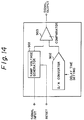
- Figure 14 is a block diagram showing an example construction of the programmable delay circuit 253 or 256 in the construction of Fig. 13.
- reference numeral 901 denotes a ramp voltage generator 902 denotes a digital to analog converter
- 903 denotes a comparator.
- the ramp voltage generator 902 generates a ramp voltage when triggered by an input of a leading edge of the MPU clock signal. The ramp voltage increases with a predetermined rate from the time of the above input of the leading edge.
- the digital to analog converter is a multiplication type digital to analog converter, outputs an analog voltage proportional to a delay time value set thereto and used as a reference voltage in the comparator 903.
- the comparator 903 compares the above ramp voltage with the above reference voltage. When the ramp voltage exceeds the reference voltage, the output of the comparator 903 rises.
- the programmable delay circuit of Fig. 14 delays the MPU clock signal by an amount determined by the delay time value set in the digital to analog converter.
- the delay time in the programmable delay circuit of Fig. 14 also has an offset. The provision for cancelling the affect of the above offset will be explained in the fifth embodiment of the present invention.
- Fig. 15 (Delay Time Measuring & Setting Circuit)
- Figure 15 is a block diagram showing an example construction of the delay time measuring & setting circuit 27 in the construction of Fig. 5.
- reference numerals 270, 271, and 273 each denote a buffer amplifier
- 272 denotes a programmable delay circuit
- 274 denotes a D-type flip-flop circuit
- 275 denotes a controller.
- reference numerals G to I respectively correspond to the denotations of the terminals of Fig. 5.
- a signal supplied from the MPU clock generator 23 is amplified through the buffer amplifier 270, and the output of the buffer amplifier 270 is divided into two ways: a way to the first delay & switch circuits 251 through the output port H, and the buffer amplifier 271 is provided on the way; and a way to an edge-triggered input terminal of the D-type flip-flop circuit 274.
- a signal input from the input port I is applied to the data input terminal of the D-type flip-flop circuit 274 through the buffer amplifier 273, and the Q output of the D-type flip-flop circuit 274 is monitored by the controller 275.
- the controller 275 controls the selectors 258 in the delay & switch circuits 251, 252, ... 25 n so that the output of the selector 254 in one of the delay & switch circuits 251, 252, ... 25 n is loop-backed toward the delay time measuring & setting circuit 27, where the delay & switch circuit at which the signal is loop-backed is connected to a processor at which the propagation delay time from the delay & switch circuit 27 is to be measured. Then, the delay & switch circuit 27 causes the master clock generator (not shown) to output a single timing pulse having a predetermined width when measuring the aforementioned propagation delay time. This operation is carried out in response to a command from the host processor 1' through the host CPU bus.
- the Q output of the D-type flip-flop circuit 274 becomes "1" when the timing of the input of the above single timing pulse into the edge-triggered input terminal of the flip-flop circuit 274 and the timing of the input of the above single timing pulse into the D input of the flip-flop circuit 274 coincide.
- the Q output of the D-type flip-flop circuit 274 becomes "1” when the delay time caused by the programmable delay circuit 272 coincides with the propagation delay time of the signal output from the output port H and then returned through the input port I. Therefore, the propagation delay time can be measured by scanning the delay time set in the programmable delay circuit 272 to find the delay time value which makes the Q output of the flip-flop circuit 274 "1". As explained before, the above measurement is carried out for all of the processors 221, 222, ... 22 n .
- the MPU clock signal is supplied from the output port c to another delay & switch circuit on the downstream side.
- the signal returning from the downstream side is input to the delay & switch circuit from the input port d, and the signal returning to the next delay & switch circuit is output from the output port b.
- Figs. 17A to 17B (Delay & Switch Circuit)
- reference numerals 221 to 224 each denote a processor
- 250', 252', 257', and 259' each denote a buffer amplifier
- 251', 252', 2541 to 2544, 2551 to 2554, 257', 258', 259', 300, 302, 307, 308, 309, and 312 each denote a selector, 2531 to 2534, 256', 304, and 305 each denote a programmable delay circuit
- 275' denotes a controller
- 3011 to 3014 and 306 each denote a D-type flip-flop circuit
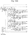
- 3031 to 3034 each denote a monostable multivibrator
- 3101 to 3104 and 3111 to 3114 each denote a level converter, 314, 315, 35
- the processors 221 to 224 are those to which the MPU clock signal is to be supplied, and the selector 300 is provided for selecting one of the processors 221 to 224 to measure the propagation delay time from the delay time measuring & setting circuits 271 to the processor.
- the programmable delay circuits 2541 to 2544 each correspond to the programmable delay circuit 253 in the construction of Fig. 13, and the programmable delay circuit 256' corresponds to the programmable delay circuit 256 in Fig. 13.
- the D-type flip-flop circuits 3011 to 3014 are provided for use in determining initial delay times in the programmable delay circuits 2531 to 2534.
- the selector 302 is provided for selecting one of the routes to be used when initially adjusting the delay times in the programmable delay circuits 2531 to 2534, and a route to be used when measuring propagation delay times for the respective processors 221 to 224.
- the level converters 3031 to 3034 and 3111 to 3114 are provided on both sides of the processors 221 to 224 for converting signal levels between ECL circuitry and TTL circuitry.
- the circuitry around the processors 221 to 224 is realized by the TTL circuitry, and the other circuitry for supplying the MPU clock signal to the processors is realized by the ECL circuitry.
- the monostable multivibrators 3031 to 3034 are provided for supplying an asynchronous request signal having a predetermined duty ratio to the processors 221 to 224 when the circuitry of Figs. 17A and 17B is used for simultaneously supplying the asynchronous request signal to the processors 221 to 224 as in the second and third embodiments of Figs. 3 and 4.
- the selectors 2541 to 2544 each correspond to the selector 254 in Fig. 13, and the selectors 2551 to 2554 each correspond to the selector 255 in Fig. 13.
- X2 denotes an edge-triggered input terminal
- H1 denotes an output terminal for the aforementioned timing signal generated in the processor.
- the programmable delay circuit 304 and the OR circuit 314 constitute a waveform shaping circuit for shaping a signal which passes therethrough
- the programmable delay circuit 305 and the OR circuit 315 constitute a waveform shaping circuit for shaping a signal which passes therethrough.
- These waveform shaping circuits are respectively provided in the path for supplying the MPU clock signal and the path for returning the MPU clock signal toward the MPU clock generator 23 in order to make symmetrical these paths.
- the D-type flip-flop circuit 306 is provided for use in determining initial delay times in the programmable delay circuits 304 and 305.
- the OR circuit 314 receives the output of the corresponding programmable delay circuit 304, and a master reset signal which is supplied from the host processor 1', and the output of the OR circuit 314 is applied to a reset input terminal of the programmable delay circuit 304.
- the OR circuit 315 receives the output of the corresponding programmable delay circuit 305, and the master reset signal, and the output of the OR circuit 315 is applied to a reset input terminal of the programmable delay circuit 305.
- the OR circuits 3531 to 3534 are respectively connected to the corresponding programmable delay circuits 2531 to 2534 in a way similar to the above waveform shaping circuits for shaping waveforms of the signals passing therethrough.
- the selector 307 is provided for selecting one of a route to be used when initially adjusting delay times in the programmable delay circuits 304 and 305, and a route to be used when the delay time measuring & setting circuit of Figs. 17A and 17B is used as a through path between the input port d to the output port b.
- the selector 308 is provided symmetricallity with the selector 300, and the selector 309 is provided for symmetricallity with the selector 302.
- the above routes, respectively provided for initially setting delay times in the programmable delay circuits 2531 to 2534 are indicated by dashed lines along the corresponding signal lines in Figs. 17A and 17B.
- the controller 275' controls the selectors in the construction of Figs. 17A and 17B so that the above indicated routes are realized. Then, the controller 275' causes the master clock generator (not shown) to output a single timing pulse having a predetermined width when measuring the aforementioned propagation delay time. This operation is carried out in response to a command from the host processor 1' through the host CPU bus.
- a signal input into the input port a is applied through the buffer amplifier 250', the selectors 251', 308, and 309 to the programmable delay circuits 2531 to 2534.
- the outputs of the programmable delay circuits 2531 to 2534 are respectively applied to the edge-triggered input terminal of the corresponding one of the flip-flop circuits 3011 to 3014.
- the output of the selector 308 is applied to one input terminal of the selector 302.
- the applied signal is selected and is output from the selector 302 to be applied to the edge-triggered input terminal of the programmable delay circuit 256'.
- the output of the programmable delay circuit 256' is applied to the D input terminal of the flip-flop circuits 3011 to 3014.
- each of the D-type flip-flop circuits 3011 to 3014 becomes the "1" level when the timing of the input of the above single timing pulse into the edge-triggered input terminal of each flip-flop circuit and the timing of the input of the above single timing pulse into the D input of the flip-flop circuit coincide.
- the Q output of each D-type flip-flop circuit becomes "1" when the delay time caused by the corresponding programmable delay circuit 253 r coincides with the propagation delay time of the signal which propagates through the programmable delay circuit 256'.
- the controller 275' initially sets in the programmable delay circuit 253 r the delay time value which makes the Q output of the flip-flop circuit 253 r "1".
- the operation for initially setting delay times in the programmable delay circuits 304 and 305 is carried out in a way similar to the above operation for setting delay times in the programmable delay circuits 2531 to 2534.
- the single timing signal input through the input port a is applied through the buffer amplifier 250' and the selector 251' to the edge-triggered input terminal of the programmable delay circuit 304 and one input terminal of the selector 307.
- the above signal is selected by the selector 307 and applied to the edge-triggered input terminal of the programmable delay circuit 305.
- the output of the programmable delay circuit 305 is applied to the edge-triggered input terminal of the D-type flip-flop circuit 306.
- the above output of the selector 251' is also applied to the edge-triggered input terminal of the programmable delay circuit 304, and the output of the programmable delay circuit 304 is applied to the D input terminal of the flip-flop circuit 306.
- the controller 275' initially sets in the programmable delay circuit 304 the delay time value which makes the Q output of the flip-flop circuit 304 "1" when the above single timing pulse is input into the circuit of Figs. 19A and 19B.
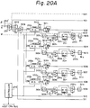
- the controller 275' controls the selectors in the construction of Figs. 17A and 17B so that the signal routes as indicated by dashed lines ⁇ , ⁇ , and ⁇ are realized, where the route ⁇ is a signal route passing from the input port a to the output port c, the route ⁇ is a signal route passing from the input port d to the output port b, and the route ⁇ is a signal route inputting from the input port a, loop-backing in the construction of Figs. 20A and 20B, and outputting from the output port b.
- the signal routes ⁇ passes through the buffer amplifier 250', the selectors 251', 308, and 309, the programmable delay circuit 2531, the level converter 3101, the selectors 2541 and 2551, the level converter 3111, the selectors 300 and 302, the programmable delay circuit 256', the selector 258, and the buffer amplifier 259', the signal routes ⁇ passes through the buffer amplifier 250', the selector 251', the programmable delay circuit 304, the selector 312, and the buffer amplifier 252', and the signal route ⁇ passes through the buffer amplifier 257', the selector 307, the programmable delay circuit 305, the selector 258, and the buffer amplifier 259'.
- the signal routes ⁇ and ⁇ are used when measuring the propagation delay time of a signal to one of the processors in the delay & switch circuit which is located on the downstream side of the construction of Figs. 20A and 20B, and the signal route ⁇ is used when measuring the propagation delay time of a signal to one of the processors in the construction of Figs. 20A and 20B.
- ⁇ 1 denotes a signal route of the MPU clock signal to be supplied to a processor in the delay & switch circuit located on the downstream side the construction of Figs. 21A and 21B
- ⁇ 2 denotes a signal route of the MPU clock signal to be supplied to a processor 221 in the construction of Figs. 21A and 21B.
- the signal route ⁇ 1 passes through the buffer amplifier 250', the selector 251', the programmable delay circuit 304, the selector 312, and the buffer amplifier 252', and the signal routes ⁇ 2 passes through the buffer amplifier 250', the selectors 251', 308, and 309, the programmable delay circuit 2531, the level converter 3101, the monostable multivibrator 3031, and the selectors 2541.
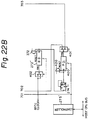
- reference numerals 271', 273', 276, 277, 278, and 279 each denote a buffer amplifier
- 272', 400, 403, 404, 410, and 411 each denote a programmable delay circuit
- 274', 405, and 412 each denote a D-type flip-flop circuit
- 275' denotes a controller
- 401, 402, 406, 407, 408, 409, 413, 414, 415, and 416 each denote a selector
- 372, 420, 423, 424, 430, and 431 each denote an OR circuit.
- the buffer amplifiers 271' and 273' respectively correspond to the buffer amplifiers 271 and 273 in Fig. 15
- the programmable delay circuit 272' corresponds to the programmable delay circuit 272 in Fig. 15
- the D-type flip-flop circuit 274' corresponds to the D-type flip-flop circuit 274 in Fig. 15
- the controller 275' corresponds to the controller 275 in Fig. 15.
- the programmable delay circuit 400 is provided for initially adjusting a delay time in the programmable delay circuit 272' for compensating the aforementioned offset in the programmable delay circuit 272'.
- the selector 401 is provided for selecting one of a route for use when initially adjusting the delay times in the programmable delay circuits 272', and a route for use when measuring the propagation delay times.
- the selector 402 is provided for the symmetry with the provision of the selector 401.
- the programmable delay circuit 403 is provided for adjusting a delay time in a path from the input port for the MPU clock signal or the input port e to the output port f.
- the programmable delay circuit 404 is provided for initially adjusting a delay time in the programmable delay circuit 403.
- the D-type flip-flop circuit 405 is provided for use when determining initial delay times in the programmable delay circuits 403 and 404.
- the selector 406 is provided for selecting one of a route to be used when initially adjusting the delay times in the programmable delay circuits 403 and 404, and a route to be used when loop-backing a signal which is input from the input port e, to the output port j.
- the selector 407 is provided for selecting one of a route to be used when initially adjusting the delay times in the programmable delay circuits 403 and 404, and a route to be used when measuring the propagation delay times.
- the selector 408 is provided for the symmetry with the provision of the selector 406.
- the selector 409 is provided symmetrically with the selector 407.
- the programmable delay circuit 410 is provided for adjusting a delay time in a path from the input port for the MPU clock signal or the input port e to the output port h, and shaping a waveform of a signal passing therethrough.
- the programmable delay circuit 411 is provided for adjusting a delay time in a path from the input port i to the output port j, and shaping a wave form of a signal passing therethrough.
- the D-type flip-flop circuit 412 is provided for determining initial delay times in the programmable delay circuits 410 and 411.
- the selector 413 is provided for selecting one of a route to be used when initially adjusting the delay times in the programmable delay circuits 410 and 411, and a route to be used when measuring the propagation delay times.
- the selector 414 is provided for the symmetry with the provision of the selector 413.
- the selector 415 is provided for selecting one of a route to be used when measuring the propagation delay times to another delay time measuring & setting circuits below the construction of Figs. 22A and 22B, and a route to be used when measuring the propagation delay times to a processor in one of the delay & switch circuits which are arrayed on the same row as the delay time measuring & setting circuit of Figs. 22A and 22B.
- the selector 416 is provided for selecting one of a route to be used for the MPU clock signal from the MPU clock input terminal of the construction of Figs. 22A and 22B, and a route to be used for the MPU clock signal supplied from the delay time measuring & setting circuit located above the construction of Figs. 22A and 22B.
- the programmable delay circuit 403 and the OR circuit 423, the programmable delay circuit 404 and the OR circuit 424, the programmable delay circuit 410 and the OR circuit 430, and the programmable delay circuit 411 and the OR circuit 431, respectively, function as a waveform shaping circuit for shaping a signal which passes therethrough.
- the above routes respectively for initially setting delay times in the programmable delay circuits 272, 400, 403, 404, 410, and 411 are indicated by dashed lines along the corresponding signal lines in Figs. 22A and 22B.
- the controller 275' controls the selectors in the construction of Figs. 22A and 22B so that the above routes as indicated by dashed lines ⁇ , ⁇ and ⁇ , are realized. Then, the controller 275' causes the master clock generator (not shown) to output a single timing pulse having a predetermined width when measuring the aforementioned propagation delay time. This operation is carried out in response to a command from the host processor 1' through the host CPU bus.
- the route ⁇ is a signal route used when the initial delay times of the programmable delay circuits 272' and 400 are determined to be set thereto.
- the initial delay times are set thereto so that a propagation delay time of a signal which passes through the selector 402 and the programmable delay circuit 272', and a propagation delay time of a signal which passes through the selector 401 and the programmable delay circuit 400 are the same.
- the initial delay times to be set are determined by the controller 275' by setting a certain delay time in one of the programmable delay circuits 272' and 400, scanning the delay time in the other of the programmable delay circuits 272' and 400, and monitoring the Q output of the D-type flip-flop circuit 274'.
- the route ⁇ is a signal route used when the initial delay times of the programmable delay circuits 403 and 404 are determined to be set thereto.
- the initial delay times are set thereto so that a propagation delay time of a signal which passes through the selector 409, the programmable delay circuit 403, and the selector 408, and a propagation delay time of a signal which passes through the selectors 406 and 407 and the programmable delay circuit 404 are the same.
- the initial delay times to be set are determined by the controller 275' by setting a certain delay time in one of the programmable delay circuits 403 and 404, scanning the delay time in the other of the programmable delay circuits 403 and 404, and monitoring the Q output of the D-type flip-flop circuit 405.
- the route ⁇ is a signal route used when the initial delay times of the programmable delay circuits 410 and 411 are determined to be set thereto.
- the initial delay times are set thereto so that a propagation delay time of a signal which passes through the programmable delay circuit 410 and the selector 414, and a propagation delay time of a signal which passes through the selector 413 and the programmable delay circuit 411 are the same.
- the initial delay times to be set are determined by the controller 275' by setting a certain delay time in one of the programmable delay circuits 410 and 411, scanning the delay time in the other of the programmable delay circuits 410 and 411, and monitoring the Q output of the D-type flip-flop circuit 412.
- the above routes are indicated by dashed lines along the corresponding signal lines in Figs. 22A and 22B.
- a signal input from the MPU clock input terminal is propagated in two ways. Namely, the signal on the first way passes through the selector 402 and the programmable delay circuit 272' to be applied to the edge-triggered input terminal of the flip-flop circuit 274', and the signal propagated on the second way passes through the selectors 416 and 409 and the programmable delay circuit 403 and is output from the output port f to be propagated to a clock input terminal of an objective processor, to be loop-backed at the clock input terminal, and to be returned therefrom.
- the returned signal is then input from the input port g, and passes through the selector 407, the programmable delay circuit 404, the selector 401, and the programmable delay circuit 400 to be applied to the D input terminal of the flip-flop circuit 274'.
- the controller 275' can measure the propagation delay time value which makes the Q output of the flip-flop circuit 274' "1" when the above single timing pulse is input into the MPU clock input terminal of the circuit of Figs. 22A and 22B.
- the above routes are indicated by dashed lines along the corresponding signal lines in Figs. 22A and 22B.
- the controller 275' controls the selectors in the construction of Figs. 22A and 22B so that the signal routes are as indicated by the dashed lines.
- a signal input from the MPU clock input terminal is propagated in two ways.
- the signal on the first way passes through the selector 402 and the programmable delay circuit 272' to be applied to the edge-triggered input terminal of the flip-flop circuit 405, and the signal propagated on the second way passes through the programmable delay circuit 410 and the selector 414 and is output from the output port h to be propagated to a clock input terminal of an objective processor, to be loop-backed at the clock input terminal, and to be returned therefrom.
- the returned signal is then input from the input port i, and passes through the selector 413, the programmable delay circuit 411, the selector 415, the selector 401, and the programmable delay circuit 400 to be applied to the D input terminal of the flip-flop circuit 274'.
- the controller 275' can measure the propagation delay time value which makes the Q output of the flip-flop circuit 274' "1" when the above single timing pulse is input to the MPU clock input terminal of the circuit of Figs. 22A and 22B.
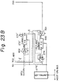
- the controller 275' controls the selectors in the construction of Figs. 22A and 22B so that the signal routes as indicated by dashed lines ⁇ and , are realized, where the route ⁇ is a signal route passing from the input port e to the output port h, and the route is a signal route passing from the input port i to the output port j.
- the signal route ⁇ passes through the buffer amplifier 276, the selector 416, the programmable delay circuit 410, the selector 414, and the buffer amplifier 277.
- the signal route passes through the buffer amplifier 278, the selector 413, the programmable delay circuit 411, the selector 415, and the buffer amplifier 279.
- the controller 275' controls the selectors in the construction of Figs. 22A and 22B so that the signal route as indicated by a dashed line is realized, where the route ⁇ is a signal route passing from the input port e to the output port h, and the route is a signal route passing from the input port i to the output port j.
- the signal routes ⁇ passes through the buffer amplifier 276, the selectors 416 and 409, the programmable delay circuit 403, the selectors 408, 406, and 407, the programmable delay circuit 404, the selector 415, and the buffer amplifier 279.
- the MPU clock signal output from the buffer amplifier 276 is propagated on the same ways ( ⁇ 1 and ⁇ 2) as the above routes ⁇ 1 and ⁇ 2, respectively.
Landscapes
- Engineering & Computer Science (AREA)
- Theoretical Computer Science (AREA)
- Physics & Mathematics (AREA)
- General Engineering & Computer Science (AREA)
- General Physics & Mathematics (AREA)
- Multi Processors (AREA)
- Test And Diagnosis Of Digital Computers (AREA)
Applications Claiming Priority (3)
| Application Number | Priority Date | Filing Date | Title |
|---|---|---|---|
| JP2171069A JP2507677B2 (ja) | 1990-06-28 | 1990-06-28 | 分散型デ―タ処理装置 |
| JP17106990 | 1990-06-28 | ||
| JP171069/90 | 1990-06-28 |
Publications (3)
| Publication Number | Publication Date |
|---|---|
| EP0464632A2 true EP0464632A2 (fr) | 1992-01-08 |
| EP0464632A3 EP0464632A3 (en) | 1993-08-25 |
| EP0464632B1 EP0464632B1 (fr) | 1999-12-08 |
Family
ID=15916461
Family Applications (1)
| Application Number | Title | Priority Date | Filing Date |
|---|---|---|---|
| EP91110561A Expired - Lifetime EP0464632B1 (fr) | 1990-06-28 | 1991-06-26 | Système et méthode de traitement de données parallèles avec compensation de décalage de signal |
Country Status (6)
| Country | Link |
|---|---|
| US (1) | US5220660A (fr) |
| EP (1) | EP0464632B1 (fr) |
| JP (1) | JP2507677B2 (fr) |
| AU (1) | AU636768B2 (fr) |
| DE (1) | DE69131822T2 (fr) |
| FI (1) | FI913114A7 (fr) |
Families Citing this family (27)
| Publication number | Priority date | Publication date | Assignee | Title |
|---|---|---|---|---|
| US5577214A (en) * | 1992-05-18 | 1996-11-19 | Opti, Inc. | Programmable hold delay |
| US5572722A (en) * | 1992-05-28 | 1996-11-05 | Texas Instruments Incorporated | Time skewing arrangement for operating random access memory in synchronism with a data processor |
| JPH0793386A (ja) * | 1993-09-28 | 1995-04-07 | Fujitsu Ltd | Lsi実装設計システム |
| US5467465A (en) * | 1993-11-17 | 1995-11-14 | Umax Data System Inc. | Two clock method for synchronizing a plurality of identical processors connected in parallel |
| JPH07248847A (ja) * | 1994-03-11 | 1995-09-26 | Fujitsu Ltd | クロック信号調整方法および装置 |
| US5768620A (en) * | 1996-04-09 | 1998-06-16 | International Business Machines Corporation | Variable timeout method in a missing-interrupt-handler for I/O requests issued by the same operating system |
| US6115769A (en) * | 1996-06-28 | 2000-09-05 | Lsi Logic Corporation | Method and apparatus for providing precise circuit delays |
| US6557066B1 (en) | 1999-05-25 | 2003-04-29 | Lsi Logic Corporation | Method and apparatus for data dependent, dual level output driver |
| US6294937B1 (en) | 1999-05-25 | 2001-09-25 | Lsi Logic Corporation | Method and apparatus for self correcting parallel I/O circuitry |
| DE10006236C2 (de) * | 2000-02-11 | 2001-12-20 | Infineon Technologies Ag | Anordnung zum Generieren von Signalimpulsen mit definierten Pulslängen in einem Baustein mit BIST-Funktion |
| JP3628265B2 (ja) * | 2001-02-21 | 2005-03-09 | 株式会社半導体理工学研究センター | マルチプロセッサシステム装置 |
| KR100414943B1 (ko) * | 2001-12-28 | 2004-01-16 | 엘지전자 주식회사 | 콤팩트 피씨아이에 기반한 다중 처리 시스템에서의 클럭분배 장치 및 방법 |
| US7043649B2 (en) * | 2002-11-20 | 2006-05-09 | Portalplayer, Inc. | System clock power management for chips with multiple processing modules |
| US7698490B2 (en) * | 2005-12-21 | 2010-04-13 | Nvidia Corporation | Passive USB power configuration switching |
| US7414550B1 (en) | 2006-06-30 | 2008-08-19 | Nvidia Corporation | Methods and systems for sample rate conversion and sample clock synchronization |
| US9209792B1 (en) | 2007-08-15 | 2015-12-08 | Nvidia Corporation | Clock selection system and method |
| US9088176B2 (en) * | 2007-12-17 | 2015-07-21 | Nvidia Corporation | Power management efficiency using DC-DC and linear regulators in conjunction |
| US8327173B2 (en) * | 2007-12-17 | 2012-12-04 | Nvidia Corporation | Integrated circuit device core power down independent of peripheral device operation |
| US9411390B2 (en) | 2008-02-11 | 2016-08-09 | Nvidia Corporation | Integrated circuit device having power domains and partitions based on use case power optimization |
| US9423846B2 (en) | 2008-04-10 | 2016-08-23 | Nvidia Corporation | Powered ring to maintain IO state independent of the core of an integrated circuit device |
| US8762759B2 (en) * | 2008-04-10 | 2014-06-24 | Nvidia Corporation | Responding to interrupts while in a reduced power state |
| JP5604799B2 (ja) * | 2009-03-06 | 2014-10-15 | 日本電気株式会社 | フォールトトレラントコンピュータ |
| JP5800752B2 (ja) * | 2012-04-25 | 2015-10-28 | 三菱電機株式会社 | 信号源同期回路 |
| US9395799B2 (en) | 2012-08-09 | 2016-07-19 | Nvidia Corporation | Power management techniques for USB interfaces |
| US9471395B2 (en) | 2012-08-23 | 2016-10-18 | Nvidia Corporation | Processor cluster migration techniques |
| US20140062561A1 (en) | 2012-09-05 | 2014-03-06 | Nvidia Corporation | Schmitt receiver systems and methods for high-voltage input signals |
| EP2775655B1 (fr) * | 2013-03-08 | 2020-10-28 | Pro Design Electronic GmbH | Procédé de distribution d'un signal d'horloge, système de distribution d'horloge et système électronique comprenant un système de distribution d'horloge |
Family Cites Families (7)
| Publication number | Priority date | Publication date | Assignee | Title |
|---|---|---|---|---|
| US4063308A (en) * | 1975-06-27 | 1977-12-13 | International Business Machines Corporation | Automatic clock tuning and measuring system for LSI computers |
| US4769558A (en) * | 1986-07-09 | 1988-09-06 | Eta Systems, Inc. | Integrated circuit clock bus layout delay system |
| JPS63238714A (ja) * | 1986-11-26 | 1988-10-04 | Hitachi Ltd | クロック供給システム |
| US4805196A (en) * | 1987-04-29 | 1989-02-14 | Gte Laboratories Incorporated | Line delay compensation for digital transmission systems utilizing low power line drivers |
| US5086500A (en) * | 1987-08-07 | 1992-02-04 | Tektronix, Inc. | Synchronized system by adjusting independently clock signals arriving at a plurality of integrated circuits |
| US5041966A (en) * | 1987-10-06 | 1991-08-20 | Nec Corporation | Partially distributed method for clock synchronization |
| US4868522A (en) * | 1988-12-13 | 1989-09-19 | Gazelle Microcircuits, Inc. | Clock signal distribution device |
-
1990
- 1990-06-28 JP JP2171069A patent/JP2507677B2/ja not_active Expired - Fee Related
-
1991
- 1991-06-25 AU AU79273/91A patent/AU636768B2/en not_active Ceased
- 1991-06-26 FI FI913114A patent/FI913114A7/fi unknown
- 1991-06-26 EP EP91110561A patent/EP0464632B1/fr not_active Expired - Lifetime
- 1991-06-26 DE DE69131822T patent/DE69131822T2/de not_active Expired - Fee Related
- 1991-06-27 US US07/722,198 patent/US5220660A/en not_active Expired - Lifetime
Also Published As
| Publication number | Publication date |
|---|---|
| JP2507677B2 (ja) | 1996-06-12 |
| EP0464632A3 (en) | 1993-08-25 |
| DE69131822D1 (de) | 2000-01-13 |
| AU636768B2 (en) | 1993-05-06 |
| FI913114A7 (fi) | 1991-12-29 |
| JPH0460742A (ja) | 1992-02-26 |
| EP0464632B1 (fr) | 1999-12-08 |
| FI913114A0 (fi) | 1991-06-26 |
| US5220660A (en) | 1993-06-15 |
| DE69131822T2 (de) | 2000-04-06 |
| AU7927391A (en) | 1992-03-26 |
Similar Documents
| Publication | Publication Date | Title |
|---|---|---|
| EP0464632A2 (fr) | Système de traitement de données parallèles avec un signal de compensation de décalage | |
| KR920005305B1 (ko) | 클록신호공급방법 및 장치 | |
| US5184027A (en) | Clock signal supply system | |
| KR100472292B1 (ko) | 동기식논리회로의신호디스큐시스템 | |
| US5712882A (en) | Signal distribution system | |
| US8819472B1 (en) | Method and system for clock edge synchronization of multiple clock distribution integrated circuits by configuring master device to produce at least one gated clock output signal | |
| US6560716B1 (en) | System for measuring delay of digital signal using clock generator and delay unit wherein a set of digital elements of clock generator identical to a set of digital elements of delay unit | |
| US20060061401A1 (en) | Semiconductor device adapted to minimize clock skew | |
| US6509775B2 (en) | Synchronous delay circuit and semiconductor integrated circuit apparatus | |
| JPS5921045B2 (ja) | クロツク信号分配回路の調整方式 | |
| JP2012181724A (ja) | クロック同期化回路及び半導体集積回路 | |
| JPH0198313A (ja) | 同期化回路 | |
| TWI473432B (zh) | 多相位時脈除頻器 | |
| KR101201871B1 (ko) | 반도체 장치 및 반도체 시스템 | |
| EP0282735A2 (fr) | Système d'alimentation de signaux d'horloge | |
| Tu et al. | A hybrid communication topology for modular multilevel converter | |
| JP3869406B2 (ja) | クロック位相差検出回路、クロック分配回路、及び大規模集積回路 | |
| JPH09134226A (ja) | クロック分配システム | |
| US8901938B2 (en) | Delay line scheme with no exit tree | |
| JP3789598B2 (ja) | 複数種類のスキューを低減する回路及び半導体装置 | |
| JP4553428B2 (ja) | プログラム可能なずれ及び周波数を有するフェーズロックループ(pll)・クロック発生器 | |
| JP2001228213A (ja) | 半導体集積回路装置及びクロックスキューの検証方法 | |
| JPS5853807B2 (ja) | クロツク折返しによる伝送方式 | |
| JPH0814609B2 (ja) | Icテスト装置 | |
| JPH09181582A (ja) | 多チャンネル遅延回路およびこれを用いた半導体集積回路試験装置 |
Legal Events
| Date | Code | Title | Description |
|---|---|---|---|
| PUAI | Public reference made under article 153(3) epc to a published international application that has entered the european phase |
Free format text: ORIGINAL CODE: 0009012 |
|
| AK | Designated contracting states |
Kind code of ref document: A2 Designated state(s): DE FR GB |
|
| PUAL | Search report despatched |
Free format text: ORIGINAL CODE: 0009013 |
|
| AK | Designated contracting states |
Kind code of ref document: A3 Designated state(s): DE FR GB |
|
| 17P | Request for examination filed |
Effective date: 19940218 |
|
| 17Q | First examination report despatched |
Effective date: 19970813 |
|
| GRAG | Despatch of communication of intention to grant |
Free format text: ORIGINAL CODE: EPIDOS AGRA |
|
| GRAG | Despatch of communication of intention to grant |
Free format text: ORIGINAL CODE: EPIDOS AGRA |
|
| GRAH | Despatch of communication of intention to grant a patent |
Free format text: ORIGINAL CODE: EPIDOS IGRA |
|
| GRAH | Despatch of communication of intention to grant a patent |
Free format text: ORIGINAL CODE: EPIDOS IGRA |
|
| GRAA | (expected) grant |
Free format text: ORIGINAL CODE: 0009210 |
|
| AK | Designated contracting states |
Kind code of ref document: B1 Designated state(s): DE FR GB |
|
| PG25 | Lapsed in a contracting state [announced via postgrant information from national office to epo] |
Ref country code: FR Free format text: LAPSE BECAUSE OF FAILURE TO SUBMIT A TRANSLATION OF THE DESCRIPTION OR TO PAY THE FEE WITHIN THE PRESCRIBED TIME-LIMIT Effective date: 19991208 |
|
| REF | Corresponds to: |
Ref document number: 69131822 Country of ref document: DE Date of ref document: 20000113 |
|
| EN | Fr: translation not filed | ||
| PLBE | No opposition filed within time limit |
Free format text: ORIGINAL CODE: 0009261 |
|
| STAA | Information on the status of an ep patent application or granted ep patent |
Free format text: STATUS: NO OPPOSITION FILED WITHIN TIME LIMIT |
|
| 26N | No opposition filed | ||
| REG | Reference to a national code |
Ref country code: GB Ref legal event code: IF02 |
|
| PGFP | Annual fee paid to national office [announced via postgrant information from national office to epo] |
Ref country code: GB Payment date: 20060621 Year of fee payment: 16 |
|
| PGFP | Annual fee paid to national office [announced via postgrant information from national office to epo] |
Ref country code: DE Payment date: 20060622 Year of fee payment: 16 |
|
| GBPC | Gb: european patent ceased through non-payment of renewal fee |
Effective date: 20070626 |
|
| PG25 | Lapsed in a contracting state [announced via postgrant information from national office to epo] |
Ref country code: DE Free format text: LAPSE BECAUSE OF NON-PAYMENT OF DUE FEES Effective date: 20080101 |
|
| PG25 | Lapsed in a contracting state [announced via postgrant information from national office to epo] |
Ref country code: GB Free format text: LAPSE BECAUSE OF NON-PAYMENT OF DUE FEES Effective date: 20070626 |