EP0567341A1 - Dispositif de puissance avec région de couche de contact de grille isolée - Google Patents
Dispositif de puissance avec région de couche de contact de grille isolée Download PDFInfo
- Publication number
- EP0567341A1 EP0567341A1 EP93303169A EP93303169A EP0567341A1 EP 0567341 A1 EP0567341 A1 EP 0567341A1 EP 93303169 A EP93303169 A EP 93303169A EP 93303169 A EP93303169 A EP 93303169A EP 0567341 A1 EP0567341 A1 EP 0567341A1
- Authority
- EP
- European Patent Office
- Prior art keywords
- gate
- region
- power device
- source electrode
- active
- Prior art date
- Legal status (The legal status is an assumption and is not a legal conclusion. Google has not performed a legal analysis and makes no representation as to the accuracy of the status listed.)
- Granted
Links
Images


Classifications
-
- H—ELECTRICITY
- H10—SEMICONDUCTOR DEVICES; ELECTRIC SOLID-STATE DEVICES NOT OTHERWISE PROVIDED FOR
- H10D—INORGANIC ELECTRIC SEMICONDUCTOR DEVICES
- H10D30/00—Field-effect transistors [FET]
- H10D30/60—Insulated-gate field-effect transistors [IGFET]
- H10D30/64—Double-diffused metal-oxide semiconductor [DMOS] FETs
- H10D30/66—Vertical DMOS [VDMOS] FETs
-
- H—ELECTRICITY
- H10—SEMICONDUCTOR DEVICES; ELECTRIC SOLID-STATE DEVICES NOT OTHERWISE PROVIDED FOR
- H10D—INORGANIC ELECTRIC SEMICONDUCTOR DEVICES
- H10D62/00—Semiconductor bodies, or regions thereof, of devices having potential barriers
- H10D62/10—Shapes, relative sizes or dispositions of the regions of the semiconductor bodies; Shapes of the semiconductor bodies
- H10D62/17—Semiconductor regions connected to electrodes not carrying current to be rectified, amplified or switched, e.g. channel regions
- H10D62/393—Body regions of DMOS transistors or IGBTs
-
- H—ELECTRICITY
- H10—SEMICONDUCTOR DEVICES; ELECTRIC SOLID-STATE DEVICES NOT OTHERWISE PROVIDED FOR
- H10D—INORGANIC ELECTRIC SEMICONDUCTOR DEVICES
- H10D30/00—Field-effect transistors [FET]
- H10D30/60—Insulated-gate field-effect transistors [IGFET]
- H10D30/64—Double-diffused metal-oxide semiconductor [DMOS] FETs
- H10D30/66—Vertical DMOS [VDMOS] FETs
- H10D30/665—Vertical DMOS [VDMOS] FETs having edge termination structures
-
- H—ELECTRICITY
- H10—SEMICONDUCTOR DEVICES; ELECTRIC SOLID-STATE DEVICES NOT OTHERWISE PROVIDED FOR
- H10D—INORGANIC ELECTRIC SEMICONDUCTOR DEVICES
- H10D62/00—Semiconductor bodies, or regions thereof, of devices having potential barriers
- H10D62/10—Shapes, relative sizes or dispositions of the regions of the semiconductor bodies; Shapes of the semiconductor bodies
- H10D62/102—Constructional design considerations for preventing surface leakage or controlling electric field concentration
- H10D62/103—Constructional design considerations for preventing surface leakage or controlling electric field concentration for increasing or controlling the breakdown voltage of reverse-biased devices
- H10D62/105—Constructional design considerations for preventing surface leakage or controlling electric field concentration for increasing or controlling the breakdown voltage of reverse-biased devices by having particular doping profiles, shapes or arrangements of PN junctions; by having supplementary regions, e.g. junction termination extension [JTE]
- H10D62/106—Constructional design considerations for preventing surface leakage or controlling electric field concentration for increasing or controlling the breakdown voltage of reverse-biased devices by having particular doping profiles, shapes or arrangements of PN junctions; by having supplementary regions, e.g. junction termination extension [JTE] having supplementary regions doped oppositely to or in rectifying contact with regions of the semiconductor bodies, e.g. guard rings with PN or Schottky junctions
Definitions
- This invention relates to preventing failure of power devices, for example, metal oxide silicon field effect transistors (MOSFETs) and insulated gate bipolar transistors (IGBTs).
- MOSFETs metal oxide silicon field effect transistors
- IGBTs insulated gate bipolar transistors
- Figure 12A is a magnified top down view of one possible configuration of one of the active cells 1102.
- Figure 12B is cross-sectional view of this configuration.
- the outer peripheral boundary 1200 of the P type peripheral body region 1201 has an octagonal shape.
- Each of the four corners formed by four large sides 1200A is blunted to form an additional small side 1200B.
- the square dotted line 1202 in Figure 12A represents the outline of the inner boundary of a contact window through which a metal source electrode contacts N+ source region 1205 and the central part 1203 of P+ type central body region 1204.
- N+ annular source region 1205 has both an octagonal outer boundary and also an octagonal inner boundary.
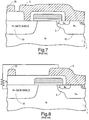
- Figure 10 is a cross-sectional view of the present invention taken along line B-B of Figure 11.
- This Figure shows a cross-sectional view of a portion of active cell 1102A, gate buffer region 1103, and a portion of gate shield region 1100.
- an N-epitaxial layer 1000 is disposed on an upper surface of a N+ substrate 1001.
- the N- epitaxial layer may, for example, be approximately 5 microns thick and may be doped with an N type dopant such as phosphorous to an approximate doping concentration of 8E15cm ⁇ 3.
- the N+ substrate 1001 is represented in Figure 10 as a thin layer for ease of illustration.
- the N+ substrate 1001 may, however, be considerably thicker than the overlying epitaxial layer 1000.
- active cell 1102A The left hand portion of active cell 1102A is shown on the right of Figure 10.
- This active cell has the same configuration as does the active cell shown in Figures 12A and 12B.
- a P+ central body region 1003 extends into the epitaxial layer 1000 from the upper surface of the epitaxial layer 1000 to an approximate depth of 2-5 microns.
- This P+ type central body region may, for example, be doped with a P type dopant such as boron to a doping concentration of 1E19cm ⁇ 3.
- a less heavily doped P type peripheral body region 1005 is disposed around the outer periphery of the P+ type central body region 1003 at the upper surface of the epitaxial layer 1000. Peripheral body region 1005 and central body region 1003 together form the body region of active cell 1102A.
- a gate buffer region 1103 of the present invention is disposed between the gate shield region 1100 of Figure 10 and the active cell 1102A of Figure 10.
- Gate buffer region 1103 may, for example, be doped with a P type dopant such as boron to a doping concentration of 1E18cm ⁇ 3 - 5E19cm ⁇ 3.
- Gate buffer region 1103 may, for example, extend from the upper surface of the epitaxial layer 1000 to an approximate depth of 2-5 microns. From a top down perspective, gate buffer region 1103 may, for example, be shaped substantially as three sides of a rectangle to separate the rectangular gate shield region 1100 from the active cells in the active region of the power device as shown in Figure 11.
- An insulating layer 1010 is disposed over the polysilicon gate layer 1009 to insulate the polysilicon gate 1009 from an overlying metal source electrode 1011.
- the overlying metal source electrode 1011 of the present invention may, for example, have the same approximate shape as does the source electrode 41 of Figure 4.
- the source electrode 1011 contacts P+ type central body region 1003 of active cell 1102A through one of the plurality of square-shaped windows in thin oxide layer 1008 and polysilicon gate layer 1009.
- the source electrode in the present invention also makes direct electrical and physical contact with the gate buffer region 1103.
Landscapes
- Insulated Gate Type Field-Effect Transistor (AREA)
- Electrodes Of Semiconductors (AREA)
Applications Claiming Priority (2)
| Application Number | Priority Date | Filing Date | Title |
|---|---|---|---|
| US873423 | 1992-04-23 | ||
| US07/873,423 US5430314A (en) | 1992-04-23 | 1992-04-23 | Power device with buffered gate shield region |
Publications (2)
| Publication Number | Publication Date |
|---|---|
| EP0567341A1 true EP0567341A1 (fr) | 1993-10-27 |
| EP0567341B1 EP0567341B1 (fr) | 1996-11-13 |
Family
ID=25361607
Family Applications (1)
| Application Number | Title | Priority Date | Filing Date |
|---|---|---|---|
| EP93303169A Expired - Lifetime EP0567341B1 (fr) | 1992-04-23 | 1993-04-22 | Dispositif de puissance avec région de couche de contact de grille isolée |
Country Status (4)
| Country | Link |
|---|---|
| US (2) | US5430314A (fr) |
| EP (1) | EP0567341B1 (fr) |
| JP (1) | JP3346825B2 (fr) |
| DE (2) | DE69305909T2 (fr) |
Cited By (2)
| Publication number | Priority date | Publication date | Assignee | Title |
|---|---|---|---|---|
| FR2741999A1 (fr) * | 1995-11-17 | 1997-06-06 | Int Rectifier Corp | Dispositif integrant un transistor bipolaire dit a grille isolee et son circuit de commande |
| EP1063705A2 (fr) * | 1999-06-24 | 2000-12-27 | Shindengen Electric Manufacturing Company, Limited | Transistor à effet de champ ayant une haute capacité de résistance au claquage |
Families Citing this family (25)
| Publication number | Priority date | Publication date | Assignee | Title |
|---|---|---|---|---|
| US5686750A (en) * | 1991-09-27 | 1997-11-11 | Koshiba & Partners | Power semiconductor device having improved reverse recovery voltage |
| DE69434937D1 (de) * | 1994-06-23 | 2007-04-19 | St Microelectronics Srl | Verfahren zur Herstellung von Leistungsbauteilen in MOS-Technologie |
| US5877529A (en) * | 1996-04-26 | 1999-03-02 | Megamos Corporation | Mosfet termination design and core cell configuration to increase breakdown voltage and to improve device ruggedness |
| US5912490A (en) * | 1997-08-04 | 1999-06-15 | Spectrian | MOSFET having buried shield plate for reduced gate/drain capacitance |
| US5918137A (en) | 1998-04-27 | 1999-06-29 | Spectrian, Inc. | MOS transistor with shield coplanar with gate electrode |
| US6215152B1 (en) | 1998-08-05 | 2001-04-10 | Cree, Inc. | MOSFET having self-aligned gate and buried shield and method of making same |
| US6621121B2 (en) * | 1998-10-26 | 2003-09-16 | Silicon Semiconductor Corporation | Vertical MOSFETs having trench-based gate electrodes within deeper trench-based source electrodes |
| US6545316B1 (en) | 2000-06-23 | 2003-04-08 | Silicon Wireless Corporation | MOSFET devices having linear transfer characteristics when operating in velocity saturation mode and methods of forming and operating same |
| WO2000074130A1 (fr) * | 1999-05-28 | 2000-12-07 | Advanced Power Devices, Inc. | Dispositif discret a diode de schottky, appauvri en courant de fuite |
| US6781194B2 (en) * | 2001-04-11 | 2004-08-24 | Silicon Semiconductor Corporation | Vertical power devices having retrograded-doped transition regions and insulated trench-based electrodes therein |
| US6784486B2 (en) * | 2000-06-23 | 2004-08-31 | Silicon Semiconductor Corporation | Vertical power devices having retrograded-doped transition regions therein |
| US20030091556A1 (en) * | 2000-12-04 | 2003-05-15 | Ruoslahti Erkki I. | Methods of inhibiting tumor growth and angiogenesis with anastellin |
| JP4198469B2 (ja) * | 2001-04-11 | 2008-12-17 | シリコン・セミコンダクター・コーポレイション | パワーデバイスとその製造方法 |
| KR100363101B1 (ko) * | 2001-04-16 | 2002-12-05 | 페어차일드코리아반도체 주식회사 | 고내압 아이솔레이션 영역을 갖는 고전압 반도체 소자 |
| ITMI20042243A1 (it) * | 2004-11-19 | 2005-02-19 | St Microelectronics Srl | Processo per la realizzazione di un dispositivo mos di potenza ad alta densita' di integrazione |
| US7875936B2 (en) * | 2004-11-19 | 2011-01-25 | Stmicroelectronics, S.R.L. | Power MOS electronic device and corresponding realizing method |
| US7751215B2 (en) | 2005-07-08 | 2010-07-06 | Panasonic Corporation | Semiconductor device and electric apparatus having a semiconductor layer divided into a plurality of square subregions |
| WO2007013367A1 (fr) | 2005-07-25 | 2007-02-01 | Matsushita Electric Industrial Co., Ltd. | Élément semi-conducteur et dispositif électrique |
| EP1909326A4 (fr) | 2005-07-26 | 2009-05-06 | Panasonic Corp | Élément à semi-conducteur et dispositif électrique |
| US8552535B2 (en) * | 2008-11-14 | 2013-10-08 | Semiconductor Components Industries, Llc | Trench shielding structure for semiconductor device and method |
| WO2010073759A1 (fr) * | 2008-12-25 | 2010-07-01 | 三菱電機株式会社 | Dispositif à semi-conducteur de puissance |
| US20130341673A1 (en) * | 2012-06-21 | 2013-12-26 | Infineon Technologies Ag | Reverse Conducting IGBT |
| US9362349B2 (en) | 2012-06-21 | 2016-06-07 | Infineon Technologies Ag | Semiconductor device with charge carrier lifetime reduction means |
| US9214521B2 (en) | 2012-06-21 | 2015-12-15 | Infineon Technologies Ag | Reverse conducting IGBT |
| US9871134B2 (en) * | 2015-12-21 | 2018-01-16 | Taiwan Semiconductor Manufacturing Company Ltd. | Power MOSFETs and methods for manufacturing the same |
Citations (13)
| Publication number | Priority date | Publication date | Assignee | Title |
|---|---|---|---|---|
| GB2137811A (en) * | 1983-03-21 | 1984-10-10 | Int Rectifier Corp | High power mosfet with direct connection from connection pads to underlying silicon |
| JPS60249367A (ja) | 1984-05-25 | 1985-12-10 | Hitachi Ltd | 絶縁ゲ−ト形トランジスタ |
| JPS6180860A (ja) * | 1984-09-28 | 1986-04-24 | Hitachi Ltd | パワ−mosfet |
| GB2166290A (en) | 1984-10-23 | 1986-04-30 | Rca Corp | Vdmos device |
| JPS6184865A (ja) * | 1984-10-02 | 1986-04-30 | Nec Corp | 半導体装置 |
| JPS6373564A (ja) * | 1986-09-16 | 1988-04-04 | Toshiba Corp | 半導体装置 |
| JPS6384070A (ja) * | 1986-09-26 | 1988-04-14 | Mitsubishi Electric Corp | 電界効果型半導体装置 |
| EP0293846A1 (fr) * | 1987-06-05 | 1988-12-07 | Siemens Aktiengesellschaft | Transistor MIS de puissance |
| US4819044A (en) | 1985-02-08 | 1989-04-04 | Nissan Motor Co., Ltd. | Vertical type MOS transistor and its chip |
| EP0335750A2 (fr) * | 1988-04-01 | 1989-10-04 | Nec Corporation | MOSFET vertical de puissance ayant une haute tension de claquage et une grande vitesse de commutation |
| JPH01276770A (ja) * | 1988-04-28 | 1989-11-07 | Fuji Electric Co Ltd | 半導体装置 |
| JPH0235780A (ja) * | 1988-07-26 | 1990-02-06 | Matsushita Electron Corp | 縦型mos電界効果トランジスタ |
| JPH03173180A (ja) * | 1989-12-01 | 1991-07-26 | Hitachi Ltd | 半導体素子 |
Family Cites Families (4)
| Publication number | Priority date | Publication date | Assignee | Title |
|---|---|---|---|---|
| US4532534A (en) * | 1982-09-07 | 1985-07-30 | Rca Corporation | MOSFET with perimeter channel |
| US4985739A (en) * | 1984-10-05 | 1991-01-15 | Analog Devices, Incorporated | Low-leakage JFET |
| JPH0282534A (ja) * | 1988-09-19 | 1990-03-23 | Sanyo Electric Co Ltd | 縦型mosfet及びその製造方法 |
| DE69029180T2 (de) * | 1989-08-30 | 1997-05-22 | Siliconix Inc | Transistor mit Spannungsbegrenzungsanordnung |
-
1992
- 1992-04-23 US US07/873,423 patent/US5430314A/en not_active Expired - Lifetime
-
1993
- 1993-04-21 JP JP11912893A patent/JP3346825B2/ja not_active Expired - Lifetime
- 1993-04-22 DE DE69305909T patent/DE69305909T2/de not_active Expired - Fee Related
- 1993-04-22 EP EP93303169A patent/EP0567341B1/fr not_active Expired - Lifetime
- 1993-04-22 DE DE0567341T patent/DE567341T1/de active Pending
-
1994
- 1994-05-13 US US08/242,519 patent/US5445978A/en not_active Expired - Lifetime
Patent Citations (13)
| Publication number | Priority date | Publication date | Assignee | Title |
|---|---|---|---|---|
| GB2137811A (en) * | 1983-03-21 | 1984-10-10 | Int Rectifier Corp | High power mosfet with direct connection from connection pads to underlying silicon |
| JPS60249367A (ja) | 1984-05-25 | 1985-12-10 | Hitachi Ltd | 絶縁ゲ−ト形トランジスタ |
| JPS6180860A (ja) * | 1984-09-28 | 1986-04-24 | Hitachi Ltd | パワ−mosfet |
| JPS6184865A (ja) * | 1984-10-02 | 1986-04-30 | Nec Corp | 半導体装置 |
| GB2166290A (en) | 1984-10-23 | 1986-04-30 | Rca Corp | Vdmos device |
| US4819044A (en) | 1985-02-08 | 1989-04-04 | Nissan Motor Co., Ltd. | Vertical type MOS transistor and its chip |
| JPS6373564A (ja) * | 1986-09-16 | 1988-04-04 | Toshiba Corp | 半導体装置 |
| JPS6384070A (ja) * | 1986-09-26 | 1988-04-14 | Mitsubishi Electric Corp | 電界効果型半導体装置 |
| EP0293846A1 (fr) * | 1987-06-05 | 1988-12-07 | Siemens Aktiengesellschaft | Transistor MIS de puissance |
| EP0335750A2 (fr) * | 1988-04-01 | 1989-10-04 | Nec Corporation | MOSFET vertical de puissance ayant une haute tension de claquage et une grande vitesse de commutation |
| JPH01276770A (ja) * | 1988-04-28 | 1989-11-07 | Fuji Electric Co Ltd | 半導体装置 |
| JPH0235780A (ja) * | 1988-07-26 | 1990-02-06 | Matsushita Electron Corp | 縦型mos電界効果トランジスタ |
| JPH03173180A (ja) * | 1989-12-01 | 1991-07-26 | Hitachi Ltd | 半導体素子 |
Non-Patent Citations (9)
| Title |
|---|
| CONFERENCE RECORD OF THE 1986 IEEE INDUSTRY APPLICATIONS SOCIETY ANNUAL MEETING vol. 1, October 1986, DENVER, COLORADO, U.S.A. pages 330 - 334 HAMZA YILMAZ ET AL 'Optimization of Power MOSFET Body Diode for Speed and Ruggedness' * |
| PATENT ABSTRACTS OF JAPAN vol. 010, no. 113 (E - 399)<2170> 26 April 1986 (1986-04-26) * |
| PATENT ABSTRACTS OF JAPAN vol. 010, no. 251 (E - 432)<2307> 28 August 1986 (1986-08-28) * |
| PATENT ABSTRACTS OF JAPAN vol. 010, no. 259 (E - 434)<2315> 4 September 1986 (1986-09-04) * |
| PATENT ABSTRACTS OF JAPAN vol. 012, no. 304 (E - 646)<3151> 18 August 1988 (1988-08-18) * |
| PATENT ABSTRACTS OF JAPAN vol. 012, no. 320 (E - 651)<3167> 30 August 1988 (1988-08-30) * |
| PATENT ABSTRACTS OF JAPAN vol. 014, no. 045 (E - 880)<3988> 26 January 1990 (1990-01-26) * |
| PATENT ABSTRACTS OF JAPAN vol. 014, no. 187 (E - 917)<4130> 16 April 1990 (1990-04-16) * |
| PATENT ABSTRACTS OF JAPAN vol. 015, no. 417 (E - 1125) 23 October 1991 (1991-10-23) * |
Cited By (2)
| Publication number | Priority date | Publication date | Assignee | Title |
|---|---|---|---|---|
| FR2741999A1 (fr) * | 1995-11-17 | 1997-06-06 | Int Rectifier Corp | Dispositif integrant un transistor bipolaire dit a grille isolee et son circuit de commande |
| EP1063705A2 (fr) * | 1999-06-24 | 2000-12-27 | Shindengen Electric Manufacturing Company, Limited | Transistor à effet de champ ayant une haute capacité de résistance au claquage |
Also Published As
| Publication number | Publication date |
|---|---|
| DE69305909T2 (de) | 1997-03-13 |
| DE69305909D1 (de) | 1996-12-19 |
| JP3346825B2 (ja) | 2002-11-18 |
| JPH07115193A (ja) | 1995-05-02 |
| EP0567341B1 (fr) | 1996-11-13 |
| DE567341T1 (de) | 1994-05-26 |
| US5445978A (en) | 1995-08-29 |
| US5430314A (en) | 1995-07-04 |
Similar Documents
| Publication | Publication Date | Title |
|---|---|---|
| EP0567341B1 (fr) | Dispositif de puissance avec région de couche de contact de grille isolée | |
| US5998836A (en) | Trench-gated power MOSFET with protective diode | |
| US6051850A (en) | Insulated gate bipolar junction transistors having built-in freewheeling diodes therein | |
| US6246092B1 (en) | High breakdown voltage MOS semiconductor apparatus | |
| EP0581246B1 (fr) | Dispositif semi-conducteur de type MIS | |
| EP1187214B1 (fr) | Dispositif semiconducteur avec une protection contre les décharges éléctrostatiques | |
| US7795638B2 (en) | Semiconductor device with a U-shape drift region | |
| EP0565349B1 (fr) | Thyristor à contrÔle MOS | |
| EP1331672B1 (fr) | MOSFET à double diffusion | |
| JPH10178176A (ja) | トレンチ・ゲート構造を有するトレンチ・ゲート形絶縁ゲート・バイポーラ・トランジスタ | |
| JPH10209432A (ja) | 半導体デバイスの改良 | |
| JPH0457111B2 (fr) | ||
| US7417282B2 (en) | Vertical double-diffused metal oxide semiconductor (VDMOS) device incorporating reverse diode | |
| JP2002353452A (ja) | 電力用半導体素子 | |
| JP4796220B2 (ja) | 保護用ダイオードを備えるトレンチゲート形パワーmosfet | |
| EP4231352B1 (fr) | Dispositif à semi-conducteur comprenant une couche de substrat avec une région de base flottante et circuit de commande de grille | |
| US5079607A (en) | Mos type semiconductor device | |
| JPH0851197A (ja) | 電流飽和特性を有するmos制御サイリスタ | |
| US20020005548A1 (en) | Trench-gate power semiconductor device preventing latch-up and method for fabricating the same | |
| US7446376B2 (en) | IGBT cathode design with improved safe operating area capability | |
| JP4177229B2 (ja) | 半導体装置とその製造方法 | |
| JP3415441B2 (ja) | 半導体装置 | |
| JP3249175B2 (ja) | 絶縁ゲート付きサイリスタ及び高耐圧半導体装置 | |
| KR102100857B1 (ko) | 전력 반도체 소자 | |
| KR0173778B1 (ko) | 반도체장치 및 그 제조방법 |
Legal Events
| Date | Code | Title | Description |
|---|---|---|---|
| PUAI | Public reference made under article 153(3) epc to a published international application that has entered the european phase |
Free format text: ORIGINAL CODE: 0009012 |
|
| AK | Designated contracting states |
Kind code of ref document: A1 Designated state(s): DE FR IT NL |
|
| ITCL | It: translation for ep claims filed |
Representative=s name: DE DOMINICIS MAYER . |
|
| EL | Fr: translation of claims filed | ||
| TCNL | Nl: translation of patent claims filed | ||
| DET | De: translation of patent claims | ||
| 17P | Request for examination filed |
Effective date: 19940426 |
|
| 17Q | First examination report despatched |
Effective date: 19950410 |
|
| GRAG | Despatch of communication of intention to grant |
Free format text: ORIGINAL CODE: EPIDOS AGRA |
|
| GRAH | Despatch of communication of intention to grant a patent |
Free format text: ORIGINAL CODE: EPIDOS IGRA |
|
| GRAH | Despatch of communication of intention to grant a patent |
Free format text: ORIGINAL CODE: EPIDOS IGRA |
|
| ITF | It: translation for a ep patent filed | ||
| GRAA | (expected) grant |
Free format text: ORIGINAL CODE: 0009210 |
|
| AK | Designated contracting states |
Kind code of ref document: B1 Designated state(s): DE FR IT NL |
|
| PG25 | Lapsed in a contracting state [announced via postgrant information from national office to epo] |
Ref country code: FR Effective date: 19961113 |
|
| REF | Corresponds to: |
Ref document number: 69305909 Country of ref document: DE Date of ref document: 19961219 |
|
| EN | Fr: translation not filed | ||
| PLBE | No opposition filed within time limit |
Free format text: ORIGINAL CODE: 0009261 |
|
| STAA | Information on the status of an ep patent application or granted ep patent |
Free format text: STATUS: NO OPPOSITION FILED WITHIN TIME LIMIT |
|
| 26N | No opposition filed | ||
| PGFP | Annual fee paid to national office [announced via postgrant information from national office to epo] |
Ref country code: NL Payment date: 20030403 Year of fee payment: 11 |
|
| PGFP | Annual fee paid to national office [announced via postgrant information from national office to epo] |
Ref country code: DE Payment date: 20040601 Year of fee payment: 12 |
|
| PG25 | Lapsed in a contracting state [announced via postgrant information from national office to epo] |
Ref country code: NL Free format text: LAPSE BECAUSE OF NON-PAYMENT OF DUE FEES Effective date: 20041101 |
|
| NLV4 | Nl: lapsed or anulled due to non-payment of the annual fee |
Effective date: 20041101 |
|
| PG25 | Lapsed in a contracting state [announced via postgrant information from national office to epo] |
Ref country code: IT Free format text: LAPSE BECAUSE OF NON-PAYMENT OF DUE FEES;WARNING: LAPSES OF ITALIAN PATENTS WITH EFFECTIVE DATE BEFORE 2007 MAY HAVE OCCURRED AT ANY TIME BEFORE 2007. THE CORRECT EFFECTIVE DATE MAY BE DIFFERENT FROM THE ONE RECORDED. Effective date: 20050422 |
|
| PG25 | Lapsed in a contracting state [announced via postgrant information from national office to epo] |
Ref country code: DE Free format text: LAPSE BECAUSE OF NON-PAYMENT OF DUE FEES Effective date: 20051101 |