EP0585601A1 - Système de sécurité pour circuit intégré et procédé d'interconnections implantées - Google Patents
Système de sécurité pour circuit intégré et procédé d'interconnections implantées Download PDFInfo
- Publication number
- EP0585601A1 EP0585601A1 EP93111978A EP93111978A EP0585601A1 EP 0585601 A1 EP0585601 A1 EP 0585601A1 EP 93111978 A EP93111978 A EP 93111978A EP 93111978 A EP93111978 A EP 93111978A EP 0585601 A1 EP0585601 A1 EP 0585601A1
- Authority
- EP
- European Patent Office
- Prior art keywords
- doped
- interconnect
- regions
- circuit
- substrate
- Prior art date
- Legal status (The legal status is an assumption and is not a legal conclusion. Google has not performed a legal analysis and makes no representation as to the accuracy of the status listed.)
- Granted
Links
Images


Classifications
-
- H—ELECTRICITY
- H10—SEMICONDUCTOR DEVICES; ELECTRIC SOLID-STATE DEVICES NOT OTHERWISE PROVIDED FOR
- H10W—GENERIC PACKAGES, INTERCONNECTIONS, CONNECTORS OR OTHER CONSTRUCTIONAL DETAILS OF DEVICES COVERED BY CLASS H10
- H10W42/00—Arrangements for protection of devices
- H10W42/40—Arrangements for protection of devices protecting against tampering, e.g. unauthorised inspection or reverse engineering
-
- G—PHYSICS
- G11—INFORMATION STORAGE
- G11C—STATIC STORES
- G11C7/00—Arrangements for writing information into, or reading information out from, a digital store
- G11C7/24—Memory cell safety or protection circuits, e.g. arrangements for preventing inadvertent reading or writing; Status cells; Test cells
-
- H—ELECTRICITY
- H10—SEMICONDUCTOR DEVICES; ELECTRIC SOLID-STATE DEVICES NOT OTHERWISE PROVIDED FOR
- H10D—INORGANIC ELECTRIC SEMICONDUCTOR DEVICES
- H10D89/00—Aspects of integrated devices not covered by groups H10D84/00 - H10D88/00
Definitions
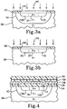
- FIGs. 3a and 3b are sectional views taken along the section lines 3a-3a and 3b-3b of FIG. 1b, respectively, illustrating the fabrication of the source, drain and interconnection implants, but excluding the polysilicon and metallization layers.
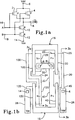
- the devices are formed in a semiconductor substrate 38 that for illustrative purposes is silicon, but may also be GaAs or some other desired semiconductor material.
- the circuit fabrication can be accomplished with a conventional process, such as that described in Frederiksen, Intuitive CMOS Electronics , McGraw-Hill Publishing Co., 1989, pages 134-145; it is a distinct advantage of the invention that it does not require any special processing to implement.
- the implantation can be performed exactly the same as in prior unsecured processes, the only difference being that the implant is now done through a larger opening in each mask that includes the implanted interconnection as well as the FET sources and drains. No differences in processing time or techniques are required, and the operator need not even know that the mask provides for circuit security.
- the circuits are then completed in a conventional manner, with threshold implants made into the FET channels to set the transistor characteristics.
- a field oxide is laid down as usual, but it also defines active areas which encompass "actual” as well as “possible” interconnect regions. Otherwise, the interconnect paths would be apparent.
- Polysilicon is then deposited and doped either by diffusion or ion implantation to form the channels and the interconnects.
- a dielectric is then deposited and metallization layers added to establish inputs, outputs and bias signals. Finally an overglass coating is laid down over the entire chip.
- a field oxide layer 54 insulates the FETs from adjacent devices, while the contact 14 to FET drain 12D is made from metallization layer 28 through an opening in an oxide insulating layer 56.
- oxide insulating layer 56 Several metallization layers separated by oxide layers are normally provided, although for simplicity only one metallization layer 28 is illustrated. This layer 28 is topped by a final oxide layer 58, and then a thicker overglass coating 60 of SiO2 that extends over the entire chip and is lightly doped so as to prevent the buildup of a static charge.
- FIG. 5 illustrates a three-input NAND gate that uses this approach; metallized connectors that are added at a later stage in the fabrication are not shown.
- the gate includes three p-channel FETs 62a, 62b and 62c, and three n-channel FETs 64a, 64b and 64c.
- Common polysilicon gate strips 66a, 66b and 66c are provided for transistor pairs 62a, 64a; 62b, 64b; and 62c, 64c, respectively.
- the polysilicon strips extend over the substrate surface between their respective FETs, as well as over the FET channels.
- To connect the upper FETs 62a-62c in parallel, their drains are electrically tied together by an interconnecting implant 60 in accordance with the invention.
- the secure NAND and NOR gates described herein and other types of logic gates can form the building blocks for many complicated logic sequences, which would therefore be virtually impossible to reverse engineer.
- a spreading resistance reverse engineering analysis might still theoretically be possible, with a small probe measuring the circuit's resistivity over a very small volume and stepped progressively across the surface, in practice this would also not work.
- the upper layers would have to be stripped away to analyze the implanted interconnects with the spreading resistance technique, but in so doing the positional registration of the implanted areas with respect to the stripped metallization would be lost.
- spreading resistance analysis is a mechanical process that is much slower than SEM analysis. The reverse engineer would still be able to see the transistors, but not the connections between them.
Landscapes
- Metal-Oxide And Bipolar Metal-Oxide Semiconductor Integrated Circuits (AREA)
- Semiconductor Integrated Circuits (AREA)
- Design And Manufacture Of Integrated Circuits (AREA)
- Internal Circuitry In Semiconductor Integrated Circuit Devices (AREA)
Priority Applications (1)
| Application Number | Priority Date | Filing Date | Title |
|---|---|---|---|
| EP98119897A EP0940851B1 (fr) | 1992-07-31 | 1993-07-28 | Système de sécurité pour circuit intégré et procédé utilisant des interconnections implantées |
Applications Claiming Priority (2)
| Application Number | Priority Date | Filing Date | Title |
|---|---|---|---|
| US92341192A | 1992-07-31 | 1992-07-31 | |
| US923411 | 1992-07-31 |
Related Child Applications (1)
| Application Number | Title | Priority Date | Filing Date |
|---|---|---|---|
| EP98119897A Division EP0940851B1 (fr) | 1992-07-31 | 1993-07-28 | Système de sécurité pour circuit intégré et procédé utilisant des interconnections implantées |
Publications (2)
| Publication Number | Publication Date |
|---|---|
| EP0585601A1 true EP0585601A1 (fr) | 1994-03-09 |
| EP0585601B1 EP0585601B1 (fr) | 1999-04-28 |
Family
ID=25448650
Family Applications (2)
| Application Number | Title | Priority Date | Filing Date |
|---|---|---|---|
| EP93111978A Expired - Lifetime EP0585601B1 (fr) | 1992-07-31 | 1993-07-28 | Système de sécurité pour circuit intégré et procédé d'interconnections implantées |
| EP98119897A Expired - Lifetime EP0940851B1 (fr) | 1992-07-31 | 1993-07-28 | Système de sécurité pour circuit intégré et procédé utilisant des interconnections implantées |
Family Applications After (1)
| Application Number | Title | Priority Date | Filing Date |
|---|---|---|---|
| EP98119897A Expired - Lifetime EP0940851B1 (fr) | 1992-07-31 | 1993-07-28 | Système de sécurité pour circuit intégré et procédé utilisant des interconnections implantées |
Country Status (5)
| Country | Link |
|---|---|
| US (3) | US5866933A (fr) |
| EP (2) | EP0585601B1 (fr) |
| JP (1) | JPH06163539A (fr) |
| DE (2) | DE69324637T2 (fr) |
| IL (1) | IL106513A (fr) |
Cited By (18)
| Publication number | Priority date | Publication date | Assignee | Title |
|---|---|---|---|---|
| EP0764985A2 (fr) | 1995-09-22 | 1997-03-26 | Hughes Aircraft Company | Circuit digital à géométrie de transistor et interrupteur de canal camouflage contre l'ingénierie inverse |
| EP0803702A3 (fr) * | 1996-04-25 | 1998-04-15 | Hewlett-Packard Company | Appareil de sonde à micro-aiguille |
| EP0883184A3 (fr) * | 1997-06-06 | 1999-12-15 | Hughes Electronics Corporation | Circuit camouflé ayant des zones implantées |
| WO2000028593A1 (fr) * | 1998-11-11 | 2000-05-18 | Infineon Technologies Ag | Procede de fabrication d'un composant semi-conducteur a cablage s'etendant par portions dans le substrat et composant semi-conducteur fabrique selon ce procede |
| EP0948052A3 (fr) * | 1998-03-12 | 2001-09-19 | Philips Patentverwaltung GmbH | Dispositif de type micro-contrôleur |
| US6667245B2 (en) | 1999-11-10 | 2003-12-23 | Hrl Laboratories, Llc | CMOS-compatible MEM switches and method of making |
| US6740942B2 (en) | 2001-06-15 | 2004-05-25 | Hrl Laboratories, Llc. | Permanently on transistor implemented using a double polysilicon layer CMOS process with buried contact |
| US6774413B2 (en) | 2001-06-15 | 2004-08-10 | Hrl Laboratories, Llc | Integrated circuit structure with programmable connector/isolator |
| US6791191B2 (en) | 2001-01-24 | 2004-09-14 | Hrl Laboratories, Llc | Integrated circuits protected against reverse engineering and method for fabricating the same using vias without metal terminations |
| US6815816B1 (en) | 2000-10-25 | 2004-11-09 | Hrl Laboratories, Llc | Implanted hidden interconnections in a semiconductor device for preventing reverse engineering |
| US6897535B2 (en) | 2002-05-14 | 2005-05-24 | Hrl Laboratories, Llc | Integrated circuit with reverse engineering protection |
| US6979606B2 (en) | 2002-11-22 | 2005-12-27 | Hrl Laboratories, Llc | Use of silicon block process step to camouflage a false transistor |
| US7049667B2 (en) | 2002-09-27 | 2006-05-23 | Hrl Laboratories, Llc | Conductive channel pseudo block process and circuit to inhibit reverse engineering |
| US7217977B2 (en) | 2004-04-19 | 2007-05-15 | Hrl Laboratories, Llc | Covert transformation of transistor properties as a circuit protection method |
| US7242063B1 (en) | 2004-06-29 | 2007-07-10 | Hrl Laboratories, Llc | Symmetric non-intrusive and covert technique to render a transistor permanently non-operable |
| US7294935B2 (en) | 2001-01-24 | 2007-11-13 | Hrl Laboratories, Llc | Integrated circuits protected against reverse engineering and method for fabricating the same using an apparent metal contact line terminating on field oxide |
| US7514755B2 (en) | 2002-12-13 | 2009-04-07 | Hrl Laboratories Llc | Integrated circuit modification using well implants |
| US7732321B2 (en) | 2004-05-17 | 2010-06-08 | Nds Limited | Method for shielding integrated circuits |
Families Citing this family (42)
| Publication number | Priority date | Publication date | Assignee | Title |
|---|---|---|---|---|
| DE69324637T2 (de) * | 1992-07-31 | 1999-12-30 | Hughes Electronics Corp., El Segundo | Sicherheitssystem für integrierte Schaltung und Verfahren mit implantierten Leitungen |
| JP3405508B2 (ja) * | 1997-05-30 | 2003-05-12 | 富士通株式会社 | 半導体集積回路 |
| US6096580A (en) * | 1999-09-24 | 2000-08-01 | International Business Machines Corporation | Low programming voltage anti-fuse |
| US6275072B1 (en) * | 1999-10-07 | 2001-08-14 | Velio Communications, Inc. | Combined phase comparator and charge pump circuit |
| US6515304B1 (en) * | 2000-06-23 | 2003-02-04 | International Business Machines Corporation | Device for defeating reverse engineering of integrated circuits by optical means |
| JP4794030B2 (ja) * | 2000-07-10 | 2011-10-12 | ルネサスエレクトロニクス株式会社 | 半導体装置 |
| JP4899248B2 (ja) * | 2001-04-02 | 2012-03-21 | 富士通セミコンダクター株式会社 | 半導体集積回路 |
| US6459629B1 (en) * | 2001-05-03 | 2002-10-01 | Hrl Laboratories, Llc | Memory with a bit line block and/or a word line block for preventing reverse engineering |
| US6924552B2 (en) * | 2002-10-21 | 2005-08-02 | Hrl Laboratories, Llc | Multilayered integrated circuit with extraneous conductive traces |
| EP1968112A3 (fr) * | 2003-02-04 | 2008-09-17 | Matsushita Electric Industrial Co., Ltd. | Dispositif à circuit intégré semi-conducteur |
| CN100468722C (zh) * | 2003-07-11 | 2009-03-11 | Nxp股份有限公司 | 对安全性敏感的半导体产品,尤其是智能卡芯片 |
| FR2865827A1 (fr) * | 2004-01-29 | 2005-08-05 | St Microelectronics Sa | Securisation du mode de test d'un circuit integre |
| US7949883B2 (en) * | 2004-06-08 | 2011-05-24 | Hrl Laboratories, Llc | Cryptographic CPU architecture with random instruction masking to thwart differential power analysis |
| US7224205B2 (en) * | 2004-07-07 | 2007-05-29 | Semi Solutions, Llc | Apparatus and method for improving drive-strength and leakage of deep submicron MOS transistors |
| US8247840B2 (en) * | 2004-07-07 | 2012-08-21 | Semi Solutions, Llc | Apparatus and method for improved leakage current of silicon on insulator transistors using a forward biased diode |
| US7683433B2 (en) * | 2004-07-07 | 2010-03-23 | Semi Solution, Llc | Apparatus and method for improving drive-strength and leakage of deep submicron MOS transistors |
| US7375402B2 (en) * | 2004-07-07 | 2008-05-20 | Semi Solutions, Llc | Method and apparatus for increasing stability of MOS memory cells |
| US7651905B2 (en) * | 2005-01-12 | 2010-01-26 | Semi Solutions, Llc | Apparatus and method for reducing gate leakage in deep sub-micron MOS transistors using semi-rectifying contacts |
| US7898297B2 (en) * | 2005-01-04 | 2011-03-01 | Semi Solution, Llc | Method and apparatus for dynamic threshold voltage control of MOS transistors in dynamic logic circuits |
| DE102005028905A1 (de) * | 2005-06-22 | 2006-12-28 | Infineon Technologies Ag | Transistorbauelement |
| FR2897439A1 (fr) * | 2006-02-15 | 2007-08-17 | St Microelectronics Sa | Circuit elelctronique comprenant un mode de test securise par l'utilisation d'un identifiant, et procede associe |
| US7863689B2 (en) * | 2006-09-19 | 2011-01-04 | Semi Solutions, Llc. | Apparatus for using a well current source to effect a dynamic threshold voltage of a MOS transistor |
| US8168487B2 (en) | 2006-09-28 | 2012-05-01 | Hrl Laboratories, Llc | Programmable connection and isolation of active regions in an integrated circuit using ambiguous features to confuse a reverse engineer |
| US7994042B2 (en) * | 2007-10-26 | 2011-08-09 | International Business Machines Corporation | Techniques for impeding reverse engineering |
| US7709401B2 (en) * | 2008-02-22 | 2010-05-04 | International Business Machines Corporation | Method of making thermally programmable anti-reverse engineering interconnects wherein interconnects only conduct when heated above room temperature |
| US10691860B2 (en) | 2009-02-24 | 2020-06-23 | Rambus Inc. | Secure logic locking and configuration with camouflaged programmable micro netlists |
| US8418091B2 (en) | 2009-02-24 | 2013-04-09 | Syphermedia International, Inc. | Method and apparatus for camouflaging a standard cell based integrated circuit |
| US8151235B2 (en) * | 2009-02-24 | 2012-04-03 | Syphermedia International, Inc. | Camouflaging a standard cell based integrated circuit |
| US9735781B2 (en) | 2009-02-24 | 2017-08-15 | Syphermedia International, Inc. | Physically unclonable camouflage structure and methods for fabricating same |
| US8510700B2 (en) | 2009-02-24 | 2013-08-13 | Syphermedia International, Inc. | Method and apparatus for camouflaging a standard cell based integrated circuit with micro circuits and post processing |
| US8111089B2 (en) * | 2009-05-28 | 2012-02-07 | Syphermedia International, Inc. | Building block for a secure CMOS logic cell library |
| JP2012054502A (ja) * | 2010-09-03 | 2012-03-15 | Elpida Memory Inc | 半導体装置 |
| US9218511B2 (en) | 2011-06-07 | 2015-12-22 | Verisiti, Inc. | Semiconductor device having features to prevent reverse engineering |
| US9287879B2 (en) * | 2011-06-07 | 2016-03-15 | Verisiti, Inc. | Semiconductor device having features to prevent reverse engineering |
| US9437555B2 (en) * | 2011-06-07 | 2016-09-06 | Verisiti, Inc. | Semiconductor device having features to prevent reverse engineering |
| US8975748B1 (en) | 2011-06-07 | 2015-03-10 | Secure Silicon Layer, Inc. | Semiconductor device having features to prevent reverse engineering |
| US9484110B2 (en) * | 2013-07-29 | 2016-11-01 | Qualcomm Incorporated | Mask-programmed read only memory with enhanced security |
| US9479176B1 (en) | 2013-12-09 | 2016-10-25 | Rambus Inc. | Methods and circuits for protecting integrated circuits from reverse engineering |
| US10568202B2 (en) | 2017-07-25 | 2020-02-18 | International Business Machines Corporation | Tamper-respondent assembly with interconnect characteristic(s) obscuring circuit layout |
| WO2019212410A1 (fr) | 2018-05-02 | 2019-11-07 | Nanyang Technological University | Cellule de disposition de circuit intégré, agencement de disposition de circuit intégré, et leurs procédés de formation |
| US10923596B2 (en) | 2019-03-08 | 2021-02-16 | Rambus Inc. | Camouflaged FinFET and method for producing same |
| DE102020105474A1 (de) | 2020-03-02 | 2021-09-02 | Infineon Technologies Ag | Integrierter Schaltkreis |
Citations (1)
| Publication number | Priority date | Publication date | Assignee | Title |
|---|---|---|---|---|
| US4291391A (en) * | 1979-09-14 | 1981-09-22 | Texas Instruments Incorporated | Taper isolated random access memory array and method of operating |
Family Cites Families (67)
| Publication number | Priority date | Publication date | Assignee | Title |
|---|---|---|---|---|
| US3946426A (en) * | 1973-03-14 | 1976-03-23 | Harris Corporation | Interconnect system for integrated circuits |
| US4267578A (en) * | 1974-08-26 | 1981-05-12 | Texas Instruments Incorporated | Calculator system with anti-theft feature |
| US4139864A (en) * | 1976-01-14 | 1979-02-13 | Schulman Lawrence S | Security system for a solid state device |
| NL185376C (nl) | 1976-10-25 | 1990-03-16 | Philips Nv | Werkwijze ter vervaardiging van een halfgeleiderinrichting. |
| US4164461A (en) * | 1977-01-03 | 1979-08-14 | Raytheon Company | Semiconductor integrated circuit structures and manufacturing methods |
| JPS54157092A (en) * | 1978-05-31 | 1979-12-11 | Nec Corp | Semiconductor integrated circuit device |
| NL7903158A (nl) | 1979-04-23 | 1980-10-27 | Philips Nv | Werkwijze voor het vervaardigen van een veldeffekt- transistor met geisoleerde poortelektrode, en transistor vervaardigd door toepassing van een derge- lijke werkwijze. |
| US4295897B1 (en) | 1979-10-03 | 1997-09-09 | Texas Instruments Inc | Method of making cmos integrated circuit device |
| US4317273A (en) | 1979-11-13 | 1982-03-02 | Texas Instruments Incorporated | Method of making high coupling ratio DMOS electrically programmable ROM |
| NL8003612A (nl) | 1980-06-23 | 1982-01-18 | Philips Nv | Werkwijze ter vervaardiging van een halfgeleider- inrichting en halfgeleiderinrichting vervaardigd door toepassing van deze werkwijze. |
| FR2486717A1 (fr) * | 1980-07-08 | 1982-01-15 | Dassault Electronique | Dispositif de transistor pour circuit integre |
| US4471376A (en) * | 1981-01-14 | 1984-09-11 | Harris Corporation | Amorphous devices and interconnect system and method of fabrication |
| JPS5856355A (ja) * | 1981-09-30 | 1983-04-04 | Hitachi Ltd | 半導体集積回路装置 |
| US4435895A (en) | 1982-04-05 | 1984-03-13 | Bell Telephone Laboratories, Incorporated | Process for forming complementary integrated circuit devices |
| JPS58190064A (ja) * | 1982-04-30 | 1983-11-05 | Hitachi Ltd | 半導体集積回路 |
| US4603381A (en) * | 1982-06-30 | 1986-07-29 | Texas Instruments Incorporated | Use of implant process for programming ROM type processor for encryption |
| JPS598352A (ja) | 1982-07-05 | 1984-01-17 | Nippon Gakki Seizo Kk | 半導体装置の製法 |
| US4623255A (en) * | 1983-10-13 | 1986-11-18 | The United States Of America As Represented By The Administrator, National Aeronautics And Space Administration | Method of examining microcircuit patterns |
| US4583011A (en) * | 1983-11-01 | 1986-04-15 | Standard Microsystems Corp. | Circuit to prevent pirating of an MOS circuit |
| US4727493A (en) * | 1984-05-04 | 1988-02-23 | Integrated Logic Systems, Inc. | Integrated circuit architecture and fabrication method therefor |
| US4821085A (en) * | 1985-05-01 | 1989-04-11 | Texas Instruments Incorporated | VLSI local interconnect structure |
| US4975756A (en) * | 1985-05-01 | 1990-12-04 | Texas Instruments Incorporated | SRAM with local interconnect |
| JPH06101551B2 (ja) | 1985-11-30 | 1994-12-12 | 日本電信電話株式会社 | Cmos集積回路装置 |
| DE3705173A1 (de) * | 1986-02-28 | 1987-09-03 | Canon Kk | Halbleitervorrichtung |
| EP0248267A3 (fr) * | 1986-06-06 | 1990-04-25 | Siemens Aktiengesellschaft | Circuit intégré monolithiques à branches de circuit parallèles entre elles |
| JPS63129647A (ja) * | 1986-11-20 | 1988-06-02 | Fujitsu Ltd | 半導体装置 |
| US5065208A (en) * | 1987-01-30 | 1991-11-12 | Texas Instruments Incorporated | Integrated bipolar and CMOS transistor with titanium nitride interconnections |
| US4766516A (en) * | 1987-09-24 | 1988-08-23 | Hughes Aircraft Company | Method and apparatus for securing integrated circuits from unauthorized copying and use |
| US4830974A (en) | 1988-01-11 | 1989-05-16 | Atmel Corporation | EPROM fabrication process |
| JPH0246762A (ja) * | 1988-08-09 | 1990-02-16 | Mitsubishi Electric Corp | 半導体集積回路 |
| US5168340A (en) | 1988-08-17 | 1992-12-01 | Texas Instruments Incorporated | Semiconductor integrated circuit device with guardring regions to prevent the formation of an MOS diode |
| JPH0777239B2 (ja) * | 1988-09-22 | 1995-08-16 | 日本電気株式会社 | 浮遊ゲート型不揮発性半導体記憶装置 |
| JPH02201935A (ja) * | 1988-12-02 | 1990-08-10 | Ncr Corp | コピー防止付回路ロジツク |
| JPH02290043A (ja) * | 1989-02-02 | 1990-11-29 | Mitsubishi Electric Corp | 半導体装置 |
| US5227649A (en) * | 1989-02-27 | 1993-07-13 | Texas Instruments Incorporated | Circuit layout and method for VLSI circuits having local interconnects |
| JPH02237038A (ja) * | 1989-03-09 | 1990-09-19 | Ricoh Co Ltd | 半導体装置 |
| DE69028665T2 (de) * | 1989-07-18 | 1997-04-17 | Sony Corp., Tokio/Tokyo | Nichtflüchtige Halbleiterspeicheranordnung und Verfahren zur Herstellung |
| US5030796A (en) * | 1989-08-11 | 1991-07-09 | Rockwell International Corporation | Reverse-engineering resistant encapsulant for microelectric device |
| US5117276A (en) * | 1989-08-14 | 1992-05-26 | Fairchild Camera And Instrument Corp. | High performance interconnect system for an integrated circuit |
| JP2501428Y2 (ja) * | 1989-12-22 | 1996-06-19 | 株式会社リコー | 熱複写装置 |
| FR2656939B1 (fr) * | 1990-01-09 | 1992-04-03 | Sgs Thomson Microelectronics | Verrous de securite pour circuit integre. |
| US5124774A (en) * | 1990-01-12 | 1992-06-23 | Paradigm Technology, Inc. | Compact SRAM cell layout |
| JPH0828120B2 (ja) * | 1990-05-23 | 1996-03-21 | 株式会社東芝 | アドレスデコード回路 |
| US5132571A (en) * | 1990-08-01 | 1992-07-21 | Actel Corporation | Programmable interconnect architecture having interconnects disposed above function modules |
| DE69133311T2 (de) | 1990-10-15 | 2004-06-24 | Aptix Corp., San Jose | Verbindungssubstrat mit integrierter Schaltung zur programmierbaren Verbindung und Probenuntersuchung |
| US5050123A (en) * | 1990-11-13 | 1991-09-17 | Intel Corporation | Radiation shield for EPROM cells |
| JP3027990B2 (ja) * | 1991-03-18 | 2000-04-04 | 富士通株式会社 | 半導体装置の製造方法 |
| US5146117A (en) * | 1991-04-01 | 1992-09-08 | Hughes Aircraft Company | Convertible multi-function microelectronic logic gate structure and method of fabricating the same |
| JP3110799B2 (ja) * | 1991-06-28 | 2000-11-20 | 株式会社東芝 | 半導体装置 |
| JPH06204414A (ja) * | 1991-07-31 | 1994-07-22 | Texas Instr Inc <Ti> | Cmos集積回路のチャネルストップ構造 |
| US5202591A (en) * | 1991-08-09 | 1993-04-13 | Hughes Aircraft Company | Dynamic circuit disguise for microelectronic integrated digital logic circuits |
| JP3118899B2 (ja) * | 1991-10-01 | 2000-12-18 | 日本電気株式会社 | アライメントチェックパターン |
| JPH05136125A (ja) * | 1991-11-14 | 1993-06-01 | Hitachi Ltd | クロツク配線及びクロツク配線を有する半導体集積回路装置 |
| US5231299A (en) * | 1992-03-24 | 1993-07-27 | International Business Machines Corporation | Structure and fabrication method for EEPROM memory cell with selective channel implants |
| JPH05275529A (ja) | 1992-03-27 | 1993-10-22 | Matsushita Electron Corp | 半導体集積回路の製造方法 |
| JPH05304207A (ja) | 1992-04-28 | 1993-11-16 | Oki Electric Ind Co Ltd | 半導体装置の素子間分離兼配線構造 |
| US5384472A (en) | 1992-06-10 | 1995-01-24 | Aspec Technology, Inc. | Symmetrical multi-layer metal logic array with continuous substrate taps and extension portions for increased gate density |
| DE69324637T2 (de) | 1992-07-31 | 1999-12-30 | Hughes Electronics Corp., El Segundo | Sicherheitssystem für integrierte Schaltung und Verfahren mit implantierten Leitungen |
| US5369299A (en) * | 1993-07-22 | 1994-11-29 | National Semiconductor Corporation | Tamper resistant integrated circuit structure |
| US5468990A (en) * | 1993-07-22 | 1995-11-21 | National Semiconductor Corp. | Structures for preventing reverse engineering of integrated circuits |
| US5354704A (en) * | 1993-07-28 | 1994-10-11 | United Microelectronics Corporation | Symmetric SRAM cell with buried N+ local interconnection line |
| US5721150A (en) | 1993-10-25 | 1998-02-24 | Lsi Logic Corporation | Use of silicon for integrated circuit device interconnection by direct writing of patterns therein |
| US5399441A (en) * | 1994-04-12 | 1995-03-21 | Dow Corning Corporation | Method of applying opaque coatings |
| US5475251A (en) * | 1994-05-31 | 1995-12-12 | National Semiconductor Corporation | Secure non-volatile memory cell |
| US5376577A (en) * | 1994-06-30 | 1994-12-27 | Micron Semiconductor, Inc. | Method of forming a low resistive current path between a buried contact and a diffusion region |
| US5783846A (en) | 1995-09-22 | 1998-07-21 | Hughes Electronics Corporation | Digital circuit with transistor geometry and channel stops providing camouflage against reverse engineering |
| US5973375A (en) | 1997-06-06 | 1999-10-26 | Hughes Electronics Corporation | Camouflaged circuit structure with step implants |
-
1993
- 1993-07-28 DE DE69324637T patent/DE69324637T2/de not_active Expired - Lifetime
- 1993-07-28 DE DE69333881T patent/DE69333881T2/de not_active Expired - Lifetime
- 1993-07-28 IL IL106513A patent/IL106513A/xx not_active IP Right Cessation
- 1993-07-28 EP EP93111978A patent/EP0585601B1/fr not_active Expired - Lifetime
- 1993-07-28 EP EP98119897A patent/EP0940851B1/fr not_active Expired - Lifetime
- 1993-08-02 JP JP5191479A patent/JPH06163539A/ja active Pending
-
1994
- 1994-02-03 US US08/191,063 patent/US5866933A/en not_active Expired - Lifetime
-
1998
- 1998-05-29 US US09/087,748 patent/US6294816B1/en not_active Expired - Lifetime
-
2000
- 2000-06-29 US US09/607,009 patent/US6613661B1/en not_active Expired - Fee Related
Patent Citations (1)
| Publication number | Priority date | Publication date | Assignee | Title |
|---|---|---|---|---|
| US4291391A (en) * | 1979-09-14 | 1981-09-22 | Texas Instruments Incorporated | Taper isolated random access memory array and method of operating |
Non-Patent Citations (1)
| Title |
|---|
| PATENT ABSTRACTS OF JAPAN vol. 016, no. 197 (P-1350)12 May 1992; & JP-A-04 028 092 (TOSHIBA CORP.) * |
Cited By (32)
| Publication number | Priority date | Publication date | Assignee | Title |
|---|---|---|---|---|
| EP0764985A2 (fr) | 1995-09-22 | 1997-03-26 | Hughes Aircraft Company | Circuit digital à géométrie de transistor et interrupteur de canal camouflage contre l'ingénierie inverse |
| EP0764985A3 (fr) * | 1995-09-22 | 1999-11-17 | Hughes Electronics Corporation | Circuit digital à géométrie de transistor et interrupteur de canal camouflage contre l'ingénierie inverse |
| EP0803702A3 (fr) * | 1996-04-25 | 1998-04-15 | Hewlett-Packard Company | Appareil de sonde à micro-aiguille |
| US5953306A (en) * | 1996-04-25 | 1999-09-14 | Hewlett-Packard Company | Micro needle probe apparatus having probes cantilevered over respective electronic circuits, moving medium memory device including same and method of making same |
| EP0883184A3 (fr) * | 1997-06-06 | 1999-12-15 | Hughes Electronics Corporation | Circuit camouflé ayant des zones implantées |
| EP0948052A3 (fr) * | 1998-03-12 | 2001-09-19 | Philips Patentverwaltung GmbH | Dispositif de type micro-contrôleur |
| WO2000028593A1 (fr) * | 1998-11-11 | 2000-05-18 | Infineon Technologies Ag | Procede de fabrication d'un composant semi-conducteur a cablage s'etendant par portions dans le substrat et composant semi-conducteur fabrique selon ce procede |
| US6440827B2 (en) | 1998-11-11 | 2002-08-27 | Infineon Technologies Ag | Method for fabricating a semiconductor component having a wiring which runs piecewise in the substrate, and also a semiconductor component which can be fabricated by this method |
| US6667245B2 (en) | 1999-11-10 | 2003-12-23 | Hrl Laboratories, Llc | CMOS-compatible MEM switches and method of making |
| GB2403593B (en) * | 2000-10-25 | 2005-07-20 | Hrl Lab Llc | Implanted hidden interconnections in a semiconductor device for preventing reverse engineering |
| US7166515B2 (en) | 2000-10-25 | 2007-01-23 | Hrl Laboratories, Llc | Implanted hidden interconnections in a semiconductor device for preventing reverse engineering |
| US6815816B1 (en) | 2000-10-25 | 2004-11-09 | Hrl Laboratories, Llc | Implanted hidden interconnections in a semiconductor device for preventing reverse engineering |
| US6791191B2 (en) | 2001-01-24 | 2004-09-14 | Hrl Laboratories, Llc | Integrated circuits protected against reverse engineering and method for fabricating the same using vias without metal terminations |
| US7294935B2 (en) | 2001-01-24 | 2007-11-13 | Hrl Laboratories, Llc | Integrated circuits protected against reverse engineering and method for fabricating the same using an apparent metal contact line terminating on field oxide |
| US6919600B2 (en) | 2001-06-15 | 2005-07-19 | Hrl Laboratories, Llc | Permanently on transistor implemented using a double polysilicon layer CMOS process with buried contact |
| US6740942B2 (en) | 2001-06-15 | 2004-05-25 | Hrl Laboratories, Llc. | Permanently on transistor implemented using a double polysilicon layer CMOS process with buried contact |
| US6893916B2 (en) | 2001-06-15 | 2005-05-17 | Hrl Laboratories, Llc | Programmable connector/isolator and double polysilicon layer CMOS process with buried contact using the same |
| US6774413B2 (en) | 2001-06-15 | 2004-08-10 | Hrl Laboratories, Llc | Integrated circuit structure with programmable connector/isolator |
| US6897535B2 (en) | 2002-05-14 | 2005-05-24 | Hrl Laboratories, Llc | Integrated circuit with reverse engineering protection |
| US7008873B2 (en) | 2002-05-14 | 2006-03-07 | Hrl Laboratories, Llc | Integrated circuit with reverse engineering protection |
| US7049667B2 (en) | 2002-09-27 | 2006-05-23 | Hrl Laboratories, Llc | Conductive channel pseudo block process and circuit to inhibit reverse engineering |
| US7888213B2 (en) | 2002-09-27 | 2011-02-15 | Hrl Laboratories, Llc | Conductive channel pseudo block process and circuit to inhibit reverse engineering |
| US8258583B1 (en) | 2002-09-27 | 2012-09-04 | Hrl Laboratories, Llc | Conductive channel pseudo block process and circuit to inhibit reverse engineering |
| US6979606B2 (en) | 2002-11-22 | 2005-12-27 | Hrl Laboratories, Llc | Use of silicon block process step to camouflage a false transistor |
| US7344932B2 (en) | 2002-11-22 | 2008-03-18 | Hrl Laboratories, Llc | Use of silicon block process step to camouflage a false transistor |
| US8679908B1 (en) | 2002-11-22 | 2014-03-25 | Hrl Laboratories, Llc | Use of silicide block process to camouflage a false transistor |
| US7514755B2 (en) | 2002-12-13 | 2009-04-07 | Hrl Laboratories Llc | Integrated circuit modification using well implants |
| US7217977B2 (en) | 2004-04-19 | 2007-05-15 | Hrl Laboratories, Llc | Covert transformation of transistor properties as a circuit protection method |
| US7732321B2 (en) | 2004-05-17 | 2010-06-08 | Nds Limited | Method for shielding integrated circuits |
| US7242063B1 (en) | 2004-06-29 | 2007-07-10 | Hrl Laboratories, Llc | Symmetric non-intrusive and covert technique to render a transistor permanently non-operable |
| US7935603B1 (en) | 2004-06-29 | 2011-05-03 | Hrl Laboratories, Llc | Symmetric non-intrusive and covert technique to render a transistor permanently non-operable |
| US8049281B1 (en) | 2004-06-29 | 2011-11-01 | Hrl Laboratories, Llc | Symmetric non-intrusive and covert technique to render a transistor permanently non-operable |
Also Published As
| Publication number | Publication date |
|---|---|
| US5866933A (en) | 1999-02-02 |
| JPH06163539A (ja) | 1994-06-10 |
| US6613661B1 (en) | 2003-09-02 |
| EP0940851B1 (fr) | 2005-10-05 |
| DE69324637T2 (de) | 1999-12-30 |
| DE69333881T2 (de) | 2006-07-13 |
| IL106513A (en) | 1997-03-18 |
| US6294816B1 (en) | 2001-09-25 |
| DE69333881D1 (de) | 2006-02-16 |
| EP0940851A1 (fr) | 1999-09-08 |
| DE69324637D1 (de) | 1999-06-02 |
| EP0585601B1 (fr) | 1999-04-28 |
Similar Documents
| Publication | Publication Date | Title |
|---|---|---|
| US5866933A (en) | Integrated circuit security system and method with implanted interconnections | |
| US5930663A (en) | Digital circuit with transistor geometry and channel stops providing camouflage against reverse engineering | |
| US6117762A (en) | Method and apparatus using silicide layer for protecting integrated circuits from reverse engineering | |
| EP0883184B1 (fr) | Utilisation d'un circuit camouflé | |
| US8524553B2 (en) | Integrated circuit modification using well implants | |
| US4513494A (en) | Late mask process for programming read only memories | |
| US4244752A (en) | Single mask method of fabricating complementary integrated circuits | |
| US7541266B2 (en) | Covert transformation of transistor properties as a circuit protection method | |
| US6504186B2 (en) | Semiconductor device having a library of standard cells and method of designing the same | |
| JP5144667B2 (ja) | リバースエンジニアリングに対する改善された抵抗力を有する半導体チップ | |
| US20130320491A1 (en) | Semiconductor Device Having Features to Prevent Reverse Engineering | |
| US5793069A (en) | Apparatus for protecting gate electrodes of target transistors in a gate array from gate charging by employing free transistors in the gate array | |
| US6774413B2 (en) | Integrated circuit structure with programmable connector/isolator | |
| US8975748B1 (en) | Semiconductor device having features to prevent reverse engineering | |
| US10037950B2 (en) | Semiconductor device having features to prevent reverse engineering | |
| EP2943979A1 (fr) | Dispositif à semi-conducteur dotés de caractéristiques permettant d'empêcher l'ingénierie inverse |
Legal Events
| Date | Code | Title | Description |
|---|---|---|---|
| PUAI | Public reference made under article 153(3) epc to a published international application that has entered the european phase |
Free format text: ORIGINAL CODE: 0009012 |
|
| AK | Designated contracting states |
Kind code of ref document: A1 Designated state(s): DE FR GB IT |
|
| 17P | Request for examination filed |
Effective date: 19940831 |
|
| 17Q | First examination report despatched |
Effective date: 19951206 |
|
| GRAG | Despatch of communication of intention to grant |
Free format text: ORIGINAL CODE: EPIDOS AGRA |
|
| GRAG | Despatch of communication of intention to grant |
Free format text: ORIGINAL CODE: EPIDOS AGRA |
|
| GRAH | Despatch of communication of intention to grant a patent |
Free format text: ORIGINAL CODE: EPIDOS IGRA |
|
| RAP1 | Party data changed (applicant data changed or rights of an application transferred) |
Owner name: HE HOLDINGS, INC. |
|
| RAP1 | Party data changed (applicant data changed or rights of an application transferred) |
Owner name: HUGHES ELECTRONICS CORPORATION |
|
| GRAH | Despatch of communication of intention to grant a patent |
Free format text: ORIGINAL CODE: EPIDOS IGRA |
|
| GRAA | (expected) grant |
Free format text: ORIGINAL CODE: 0009210 |
|
| ITF | It: translation for a ep patent filed | ||
| AK | Designated contracting states |
Kind code of ref document: B1 Designated state(s): DE FR GB IT |
|
| REF | Corresponds to: |
Ref document number: 69324637 Country of ref document: DE Date of ref document: 19990602 |
|
| ET | Fr: translation filed | ||
| PLBE | No opposition filed within time limit |
Free format text: ORIGINAL CODE: 0009261 |
|
| STAA | Information on the status of an ep patent application or granted ep patent |
Free format text: STATUS: NO OPPOSITION FILED WITHIN TIME LIMIT |
|
| 26N | No opposition filed | ||
| REG | Reference to a national code |
Ref country code: GB Ref legal event code: IF02 |
|
| PGFP | Annual fee paid to national office [announced via postgrant information from national office to epo] |
Ref country code: GB Payment date: 20120719 Year of fee payment: 20 |
|
| PGFP | Annual fee paid to national office [announced via postgrant information from national office to epo] |
Ref country code: DE Payment date: 20120720 Year of fee payment: 20 Ref country code: FR Payment date: 20120806 Year of fee payment: 20 Ref country code: IT Payment date: 20120727 Year of fee payment: 20 |
|
| REG | Reference to a national code |
Ref country code: DE Ref legal event code: R071 Ref document number: 69324637 Country of ref document: DE |
|
| REG | Reference to a national code |
Ref country code: GB Ref legal event code: PE20 Expiry date: 20130727 |
|
| PG25 | Lapsed in a contracting state [announced via postgrant information from national office to epo] |
Ref country code: DE Free format text: LAPSE BECAUSE OF EXPIRATION OF PROTECTION Effective date: 20130730 |
|
| PG25 | Lapsed in a contracting state [announced via postgrant information from national office to epo] |
Ref country code: GB Free format text: LAPSE BECAUSE OF EXPIRATION OF PROTECTION Effective date: 20130727 |