EP0601746A2 - Procédé et dispositif pour la fabrication de couches pour supports d'enregistrements optiques, procédé pour préparer une matrice et procédé pour préparer un photomasque - Google Patents
Procédé et dispositif pour la fabrication de couches pour supports d'enregistrements optiques, procédé pour préparer une matrice et procédé pour préparer un photomasque Download PDFInfo
- Publication number
- EP0601746A2 EP0601746A2 EP93309429A EP93309429A EP0601746A2 EP 0601746 A2 EP0601746 A2 EP 0601746A2 EP 93309429 A EP93309429 A EP 93309429A EP 93309429 A EP93309429 A EP 93309429A EP 0601746 A2 EP0601746 A2 EP 0601746A2
- Authority
- EP
- European Patent Office
- Prior art keywords
- roll
- stamper
- optical recording
- recording mediums
- pattern
- Prior art date
- Legal status (The legal status is an assumption and is not a legal conclusion. Google has not performed a legal analysis and makes no representation as to the accuracy of the status listed.)
- Withdrawn
Links
Images



Classifications
-
- G—PHYSICS
- G11—INFORMATION STORAGE
- G11B—INFORMATION STORAGE BASED ON RELATIVE MOVEMENT BETWEEN RECORD CARRIER AND TRANSDUCER
- G11B7/00—Recording or reproducing by optical means, e.g. recording using a thermal beam of optical radiation by modifying optical properties or the physical structure, reproducing using an optical beam at lower power by sensing optical properties; Record carriers therefor
- G11B7/24—Record carriers characterised by shape, structure or physical properties, or by the selection of the material
- G11B7/26—Apparatus or processes specially adapted for the manufacture of record carriers
-
- B—PERFORMING OPERATIONS; TRANSPORTING
- B29—WORKING OF PLASTICS; WORKING OF SUBSTANCES IN A PLASTIC STATE IN GENERAL
- B29C—SHAPING OR JOINING OF PLASTICS; SHAPING OF MATERIAL IN A PLASTIC STATE, NOT OTHERWISE PROVIDED FOR; AFTER-TREATMENT OF THE SHAPED PRODUCTS, e.g. REPAIRING
- B29C43/00—Compression moulding, i.e. applying external pressure to flow the moulding material; Apparatus therefor
- B29C43/22—Compression moulding, i.e. applying external pressure to flow the moulding material; Apparatus therefor of articles of indefinite length
- B29C43/222—Compression moulding, i.e. applying external pressure to flow the moulding material; Apparatus therefor of articles of indefinite length characterised by the shape of the surface
-
- B—PERFORMING OPERATIONS; TRANSPORTING
- B29—WORKING OF PLASTICS; WORKING OF SUBSTANCES IN A PLASTIC STATE IN GENERAL
- B29D—PRODUCING PARTICULAR ARTICLES FROM PLASTICS OR FROM SUBSTANCES IN A PLASTIC STATE
- B29D17/00—Producing carriers of records containing fine grooves or impressions, e.g. disc records for needle playback, cylinder records; Producing record discs from master stencils
- B29D17/005—Producing optically read record carriers, e.g. optical discs
- B29D17/007—Forming the relief pattern on a support larger than the record
-
- G—PHYSICS
- G11—INFORMATION STORAGE
- G11B—INFORMATION STORAGE BASED ON RELATIVE MOVEMENT BETWEEN RECORD CARRIER AND TRANSDUCER
- G11B7/00—Recording or reproducing by optical means, e.g. recording using a thermal beam of optical radiation by modifying optical properties or the physical structure, reproducing using an optical beam at lower power by sensing optical properties; Record carriers therefor
- G11B7/24—Record carriers characterised by shape, structure or physical properties, or by the selection of the material
- G11B7/26—Apparatus or processes specially adapted for the manufacture of record carriers
- G11B7/263—Preparing and using a stamper, e.g. pressing or injection molding substrates
-
- B—PERFORMING OPERATIONS; TRANSPORTING
- B29—WORKING OF PLASTICS; WORKING OF SUBSTANCES IN A PLASTIC STATE IN GENERAL
- B29C—SHAPING OR JOINING OF PLASTICS; SHAPING OF MATERIAL IN A PLASTIC STATE, NOT OTHERWISE PROVIDED FOR; AFTER-TREATMENT OF THE SHAPED PRODUCTS, e.g. REPAIRING
- B29C43/00—Compression moulding, i.e. applying external pressure to flow the moulding material; Apparatus therefor
- B29C43/32—Component parts, details or accessories; Auxiliary operations
- B29C43/44—Compression means for making articles of indefinite length
- B29C43/46—Rollers
- B29C2043/461—Rollers the rollers having specific surface features
- B29C2043/463—Rollers the rollers having specific surface features corrugated, patterned or embossed surface
-
- B—PERFORMING OPERATIONS; TRANSPORTING
- B29—WORKING OF PLASTICS; WORKING OF SUBSTANCES IN A PLASTIC STATE IN GENERAL
- B29C—SHAPING OR JOINING OF PLASTICS; SHAPING OF MATERIAL IN A PLASTIC STATE, NOT OTHERWISE PROVIDED FOR; AFTER-TREATMENT OF THE SHAPED PRODUCTS, e.g. REPAIRING
- B29C43/00—Compression moulding, i.e. applying external pressure to flow the moulding material; Apparatus therefor
- B29C43/32—Component parts, details or accessories; Auxiliary operations
- B29C43/44—Compression means for making articles of indefinite length
- B29C43/46—Rollers
- B29C2043/468—Rollers take-off rollers, i.e. arranged adjacent a material feeding device
-
- Y—GENERAL TAGGING OF NEW TECHNOLOGICAL DEVELOPMENTS; GENERAL TAGGING OF CROSS-SECTIONAL TECHNOLOGIES SPANNING OVER SEVERAL SECTIONS OF THE IPC; TECHNICAL SUBJECTS COVERED BY FORMER USPC CROSS-REFERENCE ART COLLECTIONS [XRACs] AND DIGESTS
- Y10—TECHNICAL SUBJECTS COVERED BY FORMER USPC
- Y10S—TECHNICAL SUBJECTS COVERED BY FORMER USPC CROSS-REFERENCE ART COLLECTIONS [XRACs] AND DIGESTS
- Y10S425/00—Plastic article or earthenware shaping or treating: apparatus
- Y10S425/81—Sound record
Definitions
- This invention relates to a process, and an apparatus, for continuously manufacturing substrates for optical recording mediums.
- It also relates to a process for preparing a stamper having fine patterns and a process for preparing a photomask.
- preformat pattern(s) a pattern or patterns corresponding to the preformats
- the substrates for optical recording mediums When the substrates for optical recording mediums are manufactured, it is sought, whatever their manufacturing process is, to settle two technical subjects, i.e., to improve transfer precision of preformat patterns and to decrease birefringence (or double refraction) of substrates.
- controlling the gap between the roll stamper and the molding roll causes a variation in thickness of substrate sheets.
- Such a variation in thickness of substrates for optical recording mediums further causes a non-uniformity of the quality of reproducing signals (e.g., C/N ratio) even if it is within the tolerance defined by a standard (usually, within ⁇ 10% of a standard thickness), and hence in recent years it is sought to make the variation as small as possible.
- gap variation a gap between the pattern forming surface of the roll stamper and the surface of the molding roll provided opposingly to the roll stamper to make it smaller, stated specifically, to make the gap variation, for example, 30 ⁇ m or less, particularly 20 ⁇ m or less, and more particularly 10 ⁇ m or less.
- An object of the present invention is to provide a process for manufacturing substrates for optical recording mediums, that can always maintain a small gap variation and hence can produce the substrates at a low cost, promising a superior transfer precision of preformat patterns, a low birefringence and a superior sheet thickness precision.
- Another object of the present invention is to provide an apparatus for manufacturing substrates for optical recording mediums, that can stably maintain a very small gap variation and can produce the substrates in a high quality at a low cost.
- Still another object of the present invention is to provide a process, and an apparatus, for manufacturing substrates for optical recording mediums, that can shorten the molding-fit time for the stamping molding of high-quality substrates for optical recording mediums.
- a further object of the present invention is to provide a master stamper that can give a stamper capable of more decreasing the gap variation, and a process for preparing a stamper making use of it.
- the process for manufacturing substrates for optical recording mediums is a process for successively preparing substrates for optical recording mediums, comprising the steps of; feeding a thermoplastic resin heated to a given temperature, to a gap between a roll stamper provided along its periphery with a preformat pattern and a roll provided opposingly to the roll stamper, from a means for extruding the thermoplastic resin while rotating the roll stamper and the roll at a given rotational speed; and pressing the thermoplastic resin between the roll stamper and the roll to make transfer of the preformat pattern, wherein; said thermoplastic resin is pressed between said roll stamper and said roll while bringing the former into contact with the latter through a gap control means at a region other than the region in which said roll stamper comes into touch with the thermoplastic resin on said roll.
- the process for manufacturing substrates for optical recording mediums is also a process for successively preparing substrates for optical recording mediums, comprising the steps of; feeding a thermoplastic resin heated to a given temperature, to a gap between a roll stamper comprising a roll substrate fitted along its periphery with a stamper member having a preformat pattern and a molding roll provided opposingly to the roll stamper, from a means for extruding the thermoplastic resin while rotating the roll stamper and the molding roll at a given rotational speed; and pressing the thermoplastic resin between the roll stamper and the molding roll to make transfer of the preformat pattern, wherein; said thermoplastic resin is pressed between said roll stamper and said molding roll while bringing the former into contact with the latter through a gap control means at a region other than the region in which said roll stamper comes into touch with the thermoplastic resin on said molding roll; and said stamper member is comprised of a stamper having a surface precision of 10 microns or less.
- the process for manufacturing substrates for optical recording mediums according to the present invention is still also a process for successively preparing substrates for optical recording mediums, comprising the steps of; feeding a thermoplastic resin heated to a given temperature, to a gap between a roll stamper comprising a roll substrate fitted along its periphery with a stamper member having a preformat pattern and a molding roll provided opposingly to the roll stamper, from a means for extruding the thermoplastic resin while rotating the roll stamper and the molding roll at a given rotational speed; and pressing the thermoplastic resin between the roll stamper and the molding roll to make transfer of the preformat pattern, wherein; said stamper member is comprised of a stamper having a surface precision of 10 microns or less.
- the process for manufacturing substrates for optical recording mediums is further a process for successively preparing substrates for optical recording mediums, comprising the steps of; feeding a thermoplastic resin heated to a given temperature, to a gap between a roll stamper comprising a roll substrate fitted along its periphery with a stamper member having a preformat pattern and a molding roll provided opposingly to the roll stamper, from a means for extruding the thermoplastic resin while rotating the roll stamper and the molding roll at a given rotational speed; and pressing the thermoplastic resin between the roll stamper and the molding roll to make transfer of the preformat pattern, wherein; said thermoplastic resin is pressed between said roll stamper and said molding roll while bringing the former into contact with the latter through a gap control means at a region other than the region in which said roll stamper comes into touch with the thermoplastic resin on said molding roll; and said stamper member is comprised of a stamper produced from a master stamper prepared according to the steps of; forming a pattern forming layer
- the apparatus for manufacturing substrates for optical recording mediums is an apparatus for successively preparing substrates for optical recording mediums, comprising; a means for extruding a thermoplastic resin; a roll stamper provided along its periphery with a preformat pattern; and a roll for molding the substrates for optical recording mediums by pressing the extruded resin between the roll and the roll stamper to transfer the preformat pattern to the surface of a sheet of the resin, wherein; said roll stamper and said roll are so provided as to come into contact with each other through a gap control means at a region other than the region in which said roll stamper comes into touch with the thermoplastic resin on said roll.
- the apparatus for manufacturing substrates for optical recording mediums is also an apparatus for successively preparing substrates for optical recording mediums, comprising; a means for extruding a thermoplastic resin; a roll stamper comprising a roll substrate fitted along its periphery with a stamper member having a preformat pattern; and a molding roll for molding the substrates for optical recording mediums by pressing the extruded resin between the molding roll and the roll stamper to transfer the preformat pattern to the surface of a sheet of the resin, wherein; said roll stamper and said roll are so provided as to come into contact with each other through a gap control means at a region other than the region in which said roll stamper comes into touch with the thermoplastic resin on said roll; and said stamper member is comprised of a stamper having a surface precision of 10 microns or less.
- the apparatus for manufacturing substrates for optical recording mediums is still also an apparatus for successively preparing substrates for optical recording mediums, comprising; a means for extruding a thermoplastic resin; a roll stamper comprising a roll substrate fitted along its periphery with a stamper member having a preformat pattern; and a molding roll for molding the substrates for optical recording mediums by pressing the extruded resin between the molding roll and the roll stamper to transfer the preformat pattern to the surface of a sheet of the resin, wherein; said stamper member is comprised of a stamper having a surface precision of 10 microns or less.
- the apparatus for manufacturing substrates for optical recording mediums is further an apparatus for successively preparing substrates for optical recording mediums, comprising; a means for extruding a thermoplastic resin; a roll stamper comprising a roll substrate fitted along its periphery with a stamper member having a preformat pattern; and a molding roll for molding the substrates for optical recording mediums by pressing the extruded resin between the molding roll and the roll stamper to transfer the preformat pattern to the surface of a sheet of the resin, wherein; said roll stamper and said roll are so provided as to come into contact with each other through a gap control means at a region other than the region in which said roll stamper comes into touch with the thermoplastic resin on said roll; and said stamper member is comprised of a stamper produced from a master stamper prepared according to the steps of; forming a pattern forming layer on the surface of the substrate; forming a positive resist layer on the pattern forming layer; selectively exposing the positive resist layer in accordance with the preformat pattern
- the stamper for substrates for optical recording mediums is a stamper having on its surface a preformat pattern for substrates for optical recording mediums, wherein; said stamper has a surface precision of 10 microns or less.
- the process for preparing a stamper according to the present invention is a process for preparing a stamper comprising a substrate provided in a given region of its surface, with a pattern forming member in a pattern, comprising the steps of; forming a pattern forming layer on the surface of the substrate; forming a positive resist layer on the pattern forming layer; selectively exposing the positive resist layer in accordance with said pattern and at the same time exposing the resist layer other than that in the region in which the pattern is formed; developing the resist layer to form a resist pattern; and etching the pattern forming layer, using the resist pattern as a mask.
- the process for preparing a photomask according to the present invention is a process for preparing a photomask comprising a transparent substrate provided in a given region on its surface, with a light-screening member in a pattern, comprising the steps of; forming a light-screening layer on the surface of the substrate; forming a positive resist layer on the light-screening layer; selectively exposing the positive resist layer in accordance with said pattern and at the same time exposing the resist layer other than that in the region in which the pattern is formed; developing the resist layer to form a resist pattern; and etching the pattern forming layer, using the resist pattern as a mask.
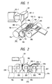
- Fig. 1 is a schematic perspective view to illustrate an embodiment of the apparatus for manufacturing substrates for optical recording mediums according to the present invention.
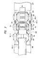
- Fig. 2 is a schematic cross section of the apparatus shown in Fig. 1.
- Fig. 3 is a schematic plan view of the apparatus shown in Fig. 1.
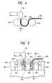
- Fig. 4 is a schematic cross section of a conventional apparatus for manufacturing substrates for optical recording mediums.
- Fig. 5 is a schematic cross section of the apparatus shown in Fig. 4.
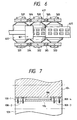
- Fig. 6 is a schematic plan view of the apparatus shown in Fig. 4.
- Fig. 7 is a schematic cross section of the part where a resin sheet is pressed between a roll and a stamper.
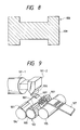
- Fig. 8 is a schematic cross section of an embodiment of the roll substrate used in the apparatus shown in Fig. 1.
- Fig. 9 is a schematic perspective view to illustrate another embodiment of the apparatus for manufacturing substrates for optical recording mediums according to the present invention.
- Fig. 10 illustrates definition of the width of the gap control means.
- Fig. 11 is a schematic perspective view to illustrate still another embodiment of the apparatus for manufacturing substrates for optical recording mediums according to the present invention.
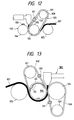
- Fig. 12 is a schematic cross section to illustrate a further embodiment of the apparatus for manufacturing substrates for optical recording mediums according to the present invention.
- Fig. 13 is a schematic cross section to illustrate a further embodiment of the apparatus for manufacturing substrates for optical recording mediums according to the present invention.
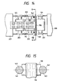
- Fig. 14 is a schematic plan view to illustrate a still further embodiment of the apparatus for manufacturing substrates for optical recording mediums according to the present invention.
- Fig. 15 is a cross section along the line B-B of the apparatus shown in Fig. 14.
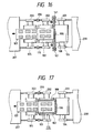
- Fig. 16 is a schematic plan view to illustrate a still further embodiment of the apparatus for manufacturing substrates for optical recording mediums according to the present invention.
- Fig. 17 is a schematic plan view to illustrate a still further embodiment of the apparatus for manufacturing substrates for optical recording mediums according to the present invention.
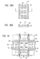
- Fig. 18A is a plan view of the stamper used in the apparatus shown in Fig. 14, and Fig. 18B is a cross section along the line C-C in Fig. 18A.
- Fig. 19 is a partial enlarged plan view to illustrate a still further embodiment of the apparatus for manufacturing substrates for optical recording mediums according to the present invention.
- Fig. 20 is a cross section in the direction laying at right angles to the rotating shaft of the roll stamper shown in Fig. 19.
- Fig. 21 is a schematic perspective view of an endless stamper usable in a still further embodiment of the apparatus for manufacturing substrates for optical recording mediums according to the present invention.
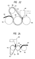
- Fig. 22 is a schematic perspective view of an apparatus for manufacturing substrates for optical recording mediums according to the present invention in which the endless stamper shown in Fig. 21 is used.
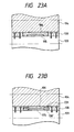
- Fig. 23A is a partial cross section of the part where the resin is pressed between a roll and a stamper, of a conventional apparatus for manufacturing substrates for optical recording mediums
- Fig. 23B is a partial cross section of the part where the resin is pressed between a roll and a stamper, of the apparatus for manufacturing substrates for optical recording mediums according to the present invention.
- Fig. 24 is a schematic cross section to illustrate a still further embodiment of the apparatus for manufacturing substrates for optical recording mediums according to the present invention.
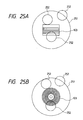
- Figs. 25A and 25B illustrate how to measure the surface precision of the stamper according to the present invention.
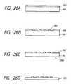
- Figs. 26A to 26D illustrate a process for preparing a conventional stamper.
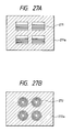
- Fig. 27A illustrates the region in which a stamper for optical cards is exposed to light
- Fig. 27B illustrates the region in which a stamper for optical disks is exposed to light.
- Fig. 28A is a plan view of a conventional stamper
- Fig. 28B is a cross section along the line D-D in Fig. 28A.
- Fig. 29 is a cross section of the stamper according to the present invention.
- Fig. 30 illustrates an instance in which the stamper according to the present invention is used as a photomask.
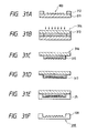
- Figs. 31A to 31F illustrate a process for preparing a stamper having the gap control means.
- Fig. 1 is a schematic perspective view of an embodiment of the apparatus for continuously manufacturing substrates for optical recording mediums according to the present invention.
- Fig. 2 is a schematic cross section of the apparatus shown in Fig. 1, in the direction laying at right angles to the rotating shaft of a roll stamper.
- Fig. 3 is a schematic plan view of the apparatus shown in Fig. 3.
- reference numeral 101 denotes a means for extruding a thermoplastic resin, comprised of an extruder 101-1 that extrudes the thermoplastic resin while melt-kneading the resin and a sheet extrusion die 101-2 that forms the thermoplastic resin into a molten resin sheet with a given width; 102, a roll stamper having on its periphery a preformat pattern 103 for optical recording mediums; and 104 and 105, molding rolls each provided opposingly to the roll stamper 102.
- the roll stamper 102 is, as shown in Fig. 7, a cross section in the direction along the rotating shaft at the part where the resin is held between the roll stamper 102 and the molding roll 104, comprised of a flexible stamper member 115 fitted along the periphery of a roll substrate 109 and also a gap control means 108 formed on the roll substrate 109 in its region other than the region in which the roll stamper comes into touch with a thermoplastic resin sheet 106.
- the roll stamper 102 and the molding rolls 104 and 105 are rotatably supported with bearings 201 to 203, respectively. These bearings are fitted to a pedestal 204 in the manner that they are each independently movable right and left as viewed in Fig. 2.
- the rolls are each formed in the manner that a heated fluid can circulate through its inside so that the surface temperature of each roll can be controlled to be a given temperature.
- the rolls are also each so constructed as to be rotatable by means of a drive motor (not shown) at a given speed in the direction shown in Fig. 2.
- the bearings 202 and 203 are also fitted with tapered blocks 202-1 and 203-1, respectively, and a wedge type space adjusting member 206 is provided between the bearings 202 and 203 in the manner that it is movable right and left as viewed in Fig. 2, on the pedestal 204 through an elevator means 205.
- This space adjusting member 206 is so shaped that it can fit to the tapered surfaces of the tapered blocks 202-1 and 203-1.
- a pressure device 207 fixed on the pedestal 204 can press the roll stamper 102 via the bearings 203 and 202 leftward as viewed in Fig. 2 and a pressure device 208 can press the molding roll 104 via the bearing 201 rightward as viewed in Fig. 2, so that the molding roll 104 and the roll stamper 102 can be brought into contact with each other through the gap control means 108.
- the thermoplastic resin sheet 106 may preferably be pressed between the the roll stamper 102 and the molding roll 104 while they are pressed against each other so as to come into contact through the gap control means 108. More specifically, since in this way the thermoplastic resin sheet is pressed between the molding roll 104 and the roll stamper 102 while they are pressed against each other so as to come into contact through the gap control means 108, the gap "d" formed by the roll stamper 102 and the molding roll 104 between which the thermoplastic resin sheet passes can be made free from its dependence on the eccentricity of each roll.
- the gap variation can be controlled to be very small, so that substrates for optical recording mediums having a superior preformat pattern sheet thickness precision and a high quality can be manufactured in a stable state and a low cost.
- the gap control means comes into contact with the periphery of the roll stamper 102, the molding-fit time (i.e., the time by which stamping molding becomes fit for obtaining the desired stamping-molded resin sheet) can be greatly shortened.
- the gap size in an apparatus for manufacturing a substrate sheet for optical recording mediums by a usual extrusion stamping molding process as shown in Fig. 4 is, as shown in Figs.
- FIG. 5 and 6 a schematic cross section and a plan view, respectively, of such an apparatus, defined by wedge type gap adjusting members 504 and 505 provided between bearings 501 to 503 that rotatably support a roll stamper 401 and specular rolls 402 and 403. More specifically, the bearings 501 to 503 are fitted with tapered blocks 501-1, 502-1 and 503-1, respectively, and the wedge type gap adjusting members 504 and 505 are provided between the bearings 501 and 502 and the bearings 502 and 503, respectively. The gap adjusting members are moved up or down to make adjustment so as to give a given gap size, and thereafter a pressure is applied to each bearing by means of pressure devices 506 and 507. In this way, the gap is controlled.
- the gap control means of the present invention is so thin and so closely comes into contact with the periphery of the roll stamper that it may cause only a very little gap variation due to thermal expansion thereof, and also any gap variations are converged in a short time so that the molding-fit time can be greatly shortened.
- the molding roll 104 may preferably be pressed against the roll stamper 102 at a total pressing force of from 490 to 11760 N (50 to 1,200 kgf), particularly from 686 to 7840 N (70 to 800 kgf), and more preferably from 980 to 4900 N (100 to 500 kgf), as a pressure applied using the pressure device 208 to the bearing 201 supporting the molding roll 104.
- This is preferable because the state of contact between the roll stamper 102 and the molding roll 104 through the gap control means 108 can not be released even if any variations more or less occur in the quantity of the thermoplastic resin being fed to the gape, and also because the roll stamper 102 and the molding roll 104 can not be hindered from being smoothly rotated.
- the roll substrate 109 having along its periphery the gap control means 108 can be formed, for example, by fixing a belt member on the roll substrate 109 at its given position, or by previously preparing an endless belt member and setting it in the roll substrate by shrinkage fitting or the like.
- this gap control means 108 there are no particular limitations thereon so long as they are materials having a uniform thickness and undergoing no deformation or change in properties due to the heat or pressure during the stamping molding. It is possible to use, for example, metal sheets made of carbon steel, copper, nickel, aluminum, etc., alloy sheets made of brass, stainless steel, etc., ceramic sheets made of BN, SiN, glass, Al2O3, titanium nitride, etc., and also heat-resistant resin sheets made of polyimide, polyether imide, aromatic polyamide, etc.
- the thickness precision of this gap control means 108 influences the gap variations, and may preferably be set within the amplitude of 10 ⁇ m or less, particularly 5 ⁇ m or less and more preferably 2 ⁇ m or less. Taking account of this thickness precision and excellent durability to heat and pressure, a stainless sheet is particularly preferred as a material for the gap control means 108 in the present embodiment.
- this gap control means 108 can be fixed on the roll substrate by a method in which it is bonded to the periphery of the roll substrate 109 by the use of an adhesive as exemplified by an organic adhesive such as an epoxy adhesive, a silicone adhesive or a cyanoacrylate adhesive, an inorganic adhesive such as water glass or low-melting glass, or a low-melting alloy, or a method in which it is mechanically secured using means such as screws as shown in Fig. 7, or a metal belt.
- an adhesive as exemplified by an organic adhesive such as an epoxy adhesive, a silicone adhesive or a cyanoacrylate adhesive, an inorganic adhesive such as water glass or low-melting glass, or a low-melting alloy, or a method in which it is mechanically secured using means such as screws as shown in Fig. 7, or a metal belt.
- the gap control means 108 is comprised of non-endless belt members 18-1, 18-2, 18-3 and 18-4, they may be in such a length that gaps (110, 111, 112 and 113) are formed between their respective ends as shown in Fig. 1 or 3, when they are wound around the roll substrate 109. This is preferable because the ends do not run against each other to cause no gap variations even if the belt members undergo expansion or elongation due to heat or pressure.
- the size of each gap may vary depending on the materials for the belt members. In usual instance, it may preferably be in the range of from 5 to 50 mm, and particularly from 10 to 40 mm.
- a plurality of belt members e.g., 108-1 and 108-2, and 108-3 and 108-4, in Fig. 1 are, as shown in Figs. 1, 3 and 7, each fixed on the periphery of the roll substrate 109 at its both ends in the width direction of the part at which the stamper member is fixed and also that the joints (with the gaps) of the belt members fixed on the both ends of the roll substrate are formed at positions different from each other on the periphery of the roll substrate 109.
- the joints (with the gaps) of the belt members fixed on the both ends of the roll substrate are formed at positions different from each other on the periphery of the roll substrate 109.
- a joint 110 of the belt member 18-1 and a joint 111 of the belt member 18-2 to be formed at different positions on the periphery of the roll substrate 109 and for a joint 112 of the belt member 18-3 and a joint 113 of the belt member 18-4 to be formed at different positions on the periphery of the roll substrate 109.
- this makes it possible for one belt member to maintain the gap size in a good precision when the joint of the other belt member comes into touch with the periphery of the molding roll 104, and is very effective for controlling the gap variations.
- the part where the stamper member is fixed on the roll substrate may be cut as shown in Fig. 8 so that the roll substrate itself can serve as the gap control means 108.
- a cleaning means 901 may be provided, to clean the surface at which the molding roll 104 comes into touch with the gap control means 108 and the surface at which the gap control means 108 comes into touch with the molding roll 104.
- the cleaning means 901 may preferably be a means that can remove dust such as resin pieces having adhered to the periphery of the molding roll 104 and the surface at which the gap control means 108 comes into touch with the molding roll 104, and also may cause no scratches on the surfaces to be cleaned.
- a wiping member may be brought into touch with the surface to be cleaned, or air may be blown thereto, any means of which can be used.
- the use of the wiping member is preferred because it has no influence on the heat balance between the thermoplastic resin sheet, the molding roll and the roll stamper.
- Materials usable for the wiping member may include polyolefin resins such as polyethylene, polypropylene and polytetrafluoroethylene, polyester resins, polyamide resins, epoxy resins, polyurethane resins, polyacrylic resins, polyvinyl chloride resins, polystyrene resins, and phenol resins.
- polyolefin resins such as polyethylene, polypropylene and polytetrafluoroethylene
- polyester resins such as polyethylene, polypropylene and polytetrafluoroethylene
- polyamide resins such as epoxy resins, polyurethane resins, polyacrylic resins, polyvinyl chloride resins, polystyrene resins, and phenol resins.
- the wiping member may also be impregnated with a solvent such as acetone, alcohol or toluene so that the cleaning can be more efficiently carried out.
- a solvent such as acetone, alcohol or toluene
- the pressure at which the wiping member is brought into touch with the surface to be cleaned may vary depending on the materials for the roll substrate and the material for the wiping member. In order to prevent the roll substrate from scratching and also remove the resin, the pressure may preferably be set in the range of from 9.8 x 10³ to 1.96 x 10⁶ Pa(0.1 kgf/cm2 to 20 kgf/cm2), and particularly from 4.9 x 10⁴ to 9.8 x 10⁵ Pa (0.5 to 10 kgf/cm2).
- the width of the gap control means may be as follows:
- the total of length "m" (see Fig. 10) at the part where the molding roll 104 comes into touch with the gap control means 108 at their one-side ends may preferably be at least 1 cm or more, particularly from 1.5 cm to 10 cm. This makes it possible to maintain the gap size more accurately and also not to make the roll substrate large-sized.
- the thickness "t" of the gap control means 108 may be as follows:
- the thickness may preferably be a thickness corresponding to the sum of the prescribed gap size "d" and the thickness "n" of the stamper member 115.
- the thickness "t" of the gap control means 108 may preferably be so set as to be substantially equal to the gap size "d".
- the gap control means 108 has been described as the one provided on the side of the roll substrate 109 of the roll stamper 102 in all instances.
- the gap control means 108 may alternatively be formed on the periphery of the molding roll 104, or may also be provided on both peripheries of the roll stamper 102 and the molding roll 104.
- Fig. 12 illustrates another embodiment of the process for manufacturing substrates for optical recording mediums according to the present invention.
- the apparatus shown in Fig. 12 comprises a gap control means 108 formed of an endless belt member, and a pulley 121 so provided that the endless belt member is synchronized with the rotation of the roll stamper 102 and led in the gap between the molding roll 104 and the roll stamper 102 so that the molding roll 104 and the roll stamper 102 are brought into contact with each other through it.
- the apparatus thus constructed makes it unnecessary to fix the gap control means 108 on the roll stamper 102 or the molding roll 104, or on the both of them, and is preferable because the gap size can be changed with ease when, for example, optical recording mediums with different thickness are formed.
- the gap control means 108 comprised of an endless belt member may be synchronized with the rotation of the molding roll 104, and also, as shown in Fig. 13, endless belt members may be suynchronized with the rotation of both the roll stamper 102 and the molding roll 104 so that the roll stamper 102 comes into contact with the molding roll 104 through two gap control means 108.
- a cleaning means 131 for cleaning the gap control means 108 may also be used so that the surface at which the gap control means 108 comes into touch with the roll stamper 102 and the surface at which it comes into touch with the molding roll 104 can be cleaned.
- a cleaning means 133 may also be provided so that the surface at which the molding roll 104 comes into touch with the gap control means 108 can be cleaned with it.
- both the each side of the gap control means 108 and the gap control means 108' may be cleaned using the cleaning means 131, so that the gap variations can be made smaller.
- the apparatus shown in Fig. 14 comprises a gap control means 108 formed of a heat-resistant disk 141 having a given thickness, and a rotating means 142 for rotating the disk 141, which is rotated as the roll stamper 102 and the molding roll 104 are rotated and is so provided as to be caught between the roll substrate 109 of the roll stamper 102 and the molding roll 104 so that the roll stamper 102 is brought into contact with the molding roll 104 through the disk 141, thereby carrying out stamping molding of the thermoplastic resin sheet 106.
- the disk 141 it is preferable for the disk 141 to be so provided that its rotational center 143 is on the plane embracing the rotating shaft of the roll stamper 102 and the rotating shaft of the molding roll 104, whereby the rotation of the disk 141 and the rotation of the roll stamper 102 and molding roll 104 may be interfered with difficulty.
- the stamping molding may be carried out on the thermoplastic resin sheet 106 while the surfaces at which the disk 141 comes into touch with the roll substrate 109 and the molding roll 104 are cleaned using a cleaning means 161 as shown in Fig. 16. This is preferable in view of the advantage that the gap variations can be made smaller.
- the stamper member 115 fixed on the periphery of the roll substrate 109 may be so formed as to have a width smaller than the width of the thermoplastic resin sheet 106.
- a press contact member 231 may preferably be provided so that the edges 106' of the resin sheet that do not come into touch with the stamper member 115 can be brought into pressure contact with the surface of the roll substrate 109 or molding roll 104.
- the edges of the resin sheet are brought into pressure contact with the periphery of the roll substrate 109 or molding roll 104 by the action of the press contact member 231 and cooled, so that the resin at the edges can be prevented from protruding to the surface at which the molding roll 104 comes into touch with the gap control means 108 and hence the gap size can be uniformly maintained even when the stamping molding is continuously carried out for a long time.
- This press contact member 231 may be provided along the periphery of the roll substrate 109, the periphery of the molding roll 104 or the peripheries of the both so long as the edges of the resin sheet 106 can be brought into pressure contact.
- an endless belt member 241 may be used as the press contact member as in the case of the gap control means 108, where the endless belt member 241 is so provided as to be led to the gap between the molding roll 104 and the roll stamper 102 by means of a pulley 242 as the molding roll 104 is rotated, so that the edges of the resin sheet 106 are brought into pressure contact with the surface of the roll substrate 109.
- Fig. 17 illustrates a further embodiment of the apparatus used in the process for manufacturing substrates for optical recording mediums according to the present invention.
- the apparatus shown in Fig. 17 comprises a gap control means 108 provided on a stamper member 170 fixed on the periphery of the roll substrate 109, in its region not coming into touch with the thermoplastic resin sheet 106.
- Fig. 18A is a schematic plan view of the stamper member 170 shown in Fig. 17, and Fig. 18B is a cross section along the line C-C in Fig. 18A.
- the stamper member 170 in the present embodiment can be prepared by, for example, a method in which the gap control means as described above is fixed, using an adhesive or screws, in a region not coming into touch with the thermoplastic resin sheet on a stamper member 180 formed by a conventional method, having a preformat pattern 103 on its surface.
- the gap control means may be fixed on the stamper member 180 at any time before the stamper member 180 is fitted to the roll substrate 109 or after the stamper member 180 has been fitted to the roll substrate 109.
- the stamper member 170 according to the present embodiment may also be prepared according to, for example, the steps as shown in Figs. 31A to 31F, where the stamper member and the gap control means 108 are integrally formed.
- a specular plate 313 is provided via a spacer 312 having a thickness equal to the gap size "d", in the manner that its specular surface faces the preformat pattern 103.
- a cell 314 is thus made up. Thereafter, the inside of the cell is packed with a photocurable resin, followed by curing to form on the specular plate a mother stamper member 316 having a resin layer 315 to which the preformat pattern has been transferred. Next, the surface (including the bared areas of the specular plate 313) of the mother stamper member 316 is made conductive, followed by electroforming to form an electroformed film 317. The electroformed film 317 is peeled from the mother stamper member 316, so that a stamper member 318 on which the gap control means 108 has been integrally formed can be obtained.
- another gap control means 194 may preferably be provided across both ends of the stamper member wound around the roll substrate.
- a method of fixing the stamper member 170 on the roll substrate 109 is exemplified by the disclosure in Japanese Patent Application No. 3-97909, filed by the present applicant, according to which, as shown in Fig. 19 and Fig. 20, the latter being a cross section of the former, fixing members 190 and 190' are secured to the back of a stamper member 170. Meanwhile, in the roll substrate 102, an engageable groove 191 to which the fixing members 190 and 190' can be fittingly inserted is formed in parallel to the axial direction of the roll substrate 109.
- the fixing members 190 and 190' are fittingly inserted to the engageable groove 191 and also wedges 192 are respectively inserted between the fixing members 190 and 190' and walls of the engageable groove 191 to apply a tension to the stamper member 170 so that the stamper member 170 can be fixed on the roll substrate 109 so as to be in close contact with the periphery thereof.
- the stamper member 170 having this gap control means 108 may be prepared in plural sheets, and the ends thereof may be joined using a means such as welding to provide an endless stamper 211 as shown in Fig. 21. Then, as shown in Fig. 22, using a pulley 221, the endless stamper 211 may be so provided as to synchronize with the rotation of a roll substrate 109 and to be caught between the molding roll 104 and the roll substrate 109 so that the stamping molding of the thermoplastic resin sheet 106 can be carried out while bringing the roll substrate 109 into contact with the molding roll 104 through the gap control means 108.
- stamper members having no gap control means 108 may be joined to produce an endless stamper and thereafter a belt made of stainless steel (which may be an endless belt) serving as the gap control means may be fixed on each side edge, whereby the endless stamper as shown in Fig. 21 can also be obtained.
- the roll stamper 102 used in the extrusion stamping molding the roll stamper comprising a roll substrate provided with a preformat pattern directly formed along its periphery or the roll stamper comprising a roll substrate fitted thereon with a stamper member having a preformat pattern is used as described above.
- the roll stamper comprising a roll substrate fitted thereon with a stamper member is preferably used because the stamper member can be replaced with ease if the preformat pattern has been broken.
- the gap variation depends also on the surface precision of the stamper member fixed on the periphery of the roll substrate.
- the gap variation so as to be 30 ⁇ m or less, particularly 20 ⁇ m or less, and more particularly 10 ⁇ m or less.
- the surface precision (flatness) of a stamper member may preferably be as follows: For example, as shown in Figs.
- a circular region 251 completely embracing a preformat pattern for a sheet of optical card or optical disk and also having an area about 12 times as large as the area of the preformat pattern has a surface precision of 15 ⁇ m or less, particularly 10 ⁇ m or less, and more particularly 5 ⁇ m or less, and also circular regions 252 of 50 mm in diameter, each having the center at any position within the above region 251, have a surface precision of 5 ⁇ m or less, and particularly 3 ⁇ m or less.
- a process for preparing a stamper for molding optical recording mediums there is a conventionally known process comprising the steps of forming a photoresist layer on a substrate, subjecting the resist layer to selective exposure and development to form a resist pattern, subsequently providing a conductive film on this resist pattern, followed by electroforming, and finally peeling the resulting electroformed film and the conductive film together from the resist pattern to give a stamper.
- a process comprising the steps of, as shown in Fig. 26, forming a pattern forming layer 262 on a substrate 261 (Fig. 26A), subsequently forming a resist pattern 263 on the pattern forming layer 262 by photolithography (Fig.
- This process enables repeated use of the master stamper, and hence has a superior mass productivity of stampers. At the same time, this process can achieve a superior pattern precision or a superior uniformity in the depth of the engraved portion in the preformat comprised of the raised and engraved portions, and is most suited for preparing stampers for optical recording mediums.
- stamper comprising a stamper member having on its surface a plurality of preformat patterns for optical recording mediums, it is very difficult to achieve the surface precision stated above.
- a master stamper formed through the following process has a very small strain, which process is a process comprising the steps of; forming a pattern forming layer on the surface of a substrate; forming a positive resist layer on the pattern forming layer; selectively exposing the positive resist layer in accordance with a preformat pattern of an optical recording medium and at the same time exposing the resist layer other than that in the region in which the pattern is formed; developing the resist layer to form a resist pattern; and etching the pattern forming layer, using the resist pattern as a mask.
- the master stamper is prepared, as described above, by forming, e.g., a chromium thin film as the pattern forming layer on a substrate having a high surface precision, thereafter coating a photoresist on the chromium thin film, followed by flood exposure using a photomask having a pattern corresponding to the preformats of optical cards or optical disks or track-by-track exposure using electron rays to print to the photoresist layer the preformat pattern corresponding to plural sheets of optical recording mediums, thereafter developing the resist layer to form a resist pattern, and then etching the chromium thin film not covered with the resist.
- the photoresist used for the preparation of the master stamper for optical recording mediums is usually a positive photoresist having an excellent resolution.
- the chromium thin film formed in the region where the photoresist layer is not exposed in the above process for preparing the master stamper i.e., the region as exemplified by a region 271a outside the pattern regions 271 of an optical card shown in Fig. 27A, which illustrates exposure regions, or a region 272a present outside pattern regions 272 of an optical disk shown in Fig. 27B, remains as it is as shown in Fig. 28B, which is a cross section of the line D-D in Fig. 28A schematically showing a plan view of the master stamper finally obtained.
- the chromium thin film is usually produced by sputtering of chromium on a polished glass substrate under such conditions as to cause no tensile stress or compression stress to prevent the glass substrate from warping when the film is formed on one side of the glass substrate, the chromium is partly removed by etching in the region in which the preformat pattern is formed, and therefore the stress kept balanced until that time becomes imbalanced in the chromium thin film formed in the vicinity of the pattern, resulting in lack of stress balance, and consequently causing a strain in the master stamper.
- the chromium thin film formed in the regon 271a or 272a is removed to make the substrate surface bare in this region, so that the influence of stress the chromium thin film may have on the substrate can be greatly reduced.
- any strain produced in the master stamper can be made smaller.
- the master stamper of the present invention can be prepared in the following way:
- a metal as exemplified by chromium is deposited by a method such as vacuum deposition or sputtering to form a film as a pattern forming layer in a thickness corresponding to the depth of information track grooves or information pits (usually a thickness of from 500 to 5,000 ⁇ is preferable).
- a positive photoresist layer is superposed on the pattern forming layer and thereafter the photoresist layer is subjected to pattern exposure or irradiation with electron rays corresponding to the tracking grooves or information pits.
- a photoresist should preferably be applied by spin coating.
- the photoresist layer should preferably be in a thickness of from 500 to 1,500 ⁇ . If it has a layer thickness of less than 500 ⁇ , the thin film with a uniform thickness is difficult to form by the spin coating, where defects such as pinholes tend to occur.
- the chromium thin film not covered with the photoresist is etched away.
- the etching is carried out in a depth corresponding to the thickness of the chromium thin film, and well carried out so that the glass substrate surface can be completely laid bare.
- a master stamper 291 of the present invention having a cross section as shown in Fig. 29.
- the master stamper according to the present invention is subsequently used in the preparation of the stamper for molding substrates for optical recording mediums.
- the stamper can be prepared from the master stamper by a process including, as previously described, a process comprising forming a conductive film on the surface of the master stamper, thereafter forming an electroformed film on the conductive film, and then separating the electroformed film together with the conductive film from the master stamper to obtain a stamper, and a process comprising making a replica of the master stamper by the use of a photocurable resin, forming a conductive film on the surface of the replica, thereafter forming an electroformed film on the conductive film, and then separating the electroformed film together with the conductive film from the replica to obtain a stamper.
- the gap variation can be controlled to be 30 ⁇ m or less, and further 20 ⁇ m or less, so that it becomes possible to mass-produce substrates for optical recording mediums with a very high quality.
- a product in which the substrate is replaced by a transparent substrate (e.g., glass) and the pattern forming layer is formed of a light-screening material (e.g., chromium) can also be preferably used as a photomask. More specifically, for example, as shown in Fig.
- a master stamper 304 previously prepared by the process of the present invention which is usable as the photomask, is provided on the photoresist layer, followed by exposure, whereby the preformat pattern can be accurately printed on the resist layer because of a small strain produced in the photomask itself.
- the exposure carried out on the regions 271a and 272a of the photomask can be carried out at the same time when the preformat pattern is printed, so that master stampers having a good surface precision and also more improved in pattern precision can be prepared in a good efficiency.
- the surface temperature of the roll stamper 102 and the molding rolls 104 and 105 may vary depending on the resin used.
- the roll stamper 102 may usually be set at a temperature of from 110°C to 145°C, the molding roll 104 from 90°C to 135°C, and the molding roll 105 from 120°C to 150°C, taking account of the heat deformation temperature of the polycarbonate.
- the roll stamper 102 may be set at a temperature of from 120°C to 145°C, the molding roll 104 from 100°C to 135, and the molding roll 105 from 120°C to 150°C.
- These roll temperatures may be controlled, for example, using a heater casted in each roll or by circulating a heating medium through the center of each roll.
- the resin used as a material for the resin sheet or substrate sheet 106 is a thermoplastic resin, and may preferably be those having a high transmittance to the light for recording and reproducing, including, for example, acrylic resins, polyester resins, polycarbonate resins, vinyl resins, polysulfone resins, polyolefin resins and cellulose derivatives.
- the molding rolls 104 and 105 and the roll substrate 109 of the roll stamper 102 may preferably be made of materials having a high hardness, having a good heat conductivity and capable of being readily mirror-finished.
- materials having a high hardness having a good heat conductivity and capable of being readily mirror-finished.
- steel, chrome steel, aluminum, mold steel (maraging steel) and so forth can be used.
- thermoplastic resin (a molten resin sheet) having been stamping-molded between the roll stamper 102 and the molding rolls 104 and 105 is formed into a substrate sheet 107 for optical recording mediums.
- the substrate sheet 107 thus obtained is wound up on a roll and forwarded to the subsequent steps of forming a recording layer and/or a reflective layer, forming a protective layer, and forming a hard coat layer on the recording and/or reproducing light incident surface of the substrate sheet 107 for optical recording mediums.
- the above steps may be carried out continuously.
- the recoring layer formed on the surface of the substrate sheet 107 for optical recording mediums, on the side on which the preformats have been transferred may be comprised of, for example, an oxide of Te, Sb, Mo, Ge, V, Sn, etc., an inorganic compound such as Sn or TeO x -Ge, a composite of a metal and an organic compound or inorganic sulfide, such as TeCH4, TeCS2, Te-styrene, Sn-SO2, GeS-Sn or SnS-S, a material of a thermoplastic resin such as nitrocelluloce, polystyrene or polyethylene having particles of metal such as silver dispersed thereinto. Chalcogens, and also magnetic materials such as Tb-Fe-Co, Gd-Fe-Co, Tb-Fe-Co-Cr and Gd-Fe-Co-Cr, as well as organic coloring matters may also be used.
- the preformat pattern may specifically include, for example, a pattern corresponding to tracking tracks for optical disks or optical cards, having the form of a spiral, concentric circles or stripes with a width of from 1 ⁇ m to 4 ⁇ m, a pitch of from 1 ⁇ m to 20 ⁇ m and a depth or height of from 200 ⁇ to 5,000 ⁇ , and a pattern corresponding to address pits with a width of from 0.6 ⁇ m to 10 ⁇ m, a length of from 0.6 ⁇ m to 20 ⁇ m and a depth or height of from 200 ⁇ to 5,000 ⁇ .
- the address pits include those which form raised portions or engraved portions with respect to the surfaces of the substrates for optical recording mediums.
- the stamping molding is carried out by bringing the roll stamper into contact with the molding roll through the gap control means, whereby the gap variation can be made smaller even when a roll stamper and a molding roll each having a large eccentricity are used, so that molding stability can be improved and high-quality substrates for optical recording mediums having a superior sheet thickness precision can be manufactured at a low cost.
- the present invention makes it unnecessary to use the conventional gap adjusting member, and hence the time for which the stamping molding becomes stable after the start-up of the apparatus can be shortened, making it possible to decrease the quantity of resins having been hitherto wasted.
- the process for preparing a master stamper according to the present invention also makes it possible to obtain a master stamper with a superior surface precision.
- Use of the master stamper prepared by this process also makes it possible to prepare a stamper having a superior surface precision.
- Use of the roll stamper comprising the roll substrate fitted thereon with this stamper having a superior surface precision also makes it possible to allow the gap variation to be always very small, e.g., not more than 30 ⁇ m, and particularly not more than 20 ⁇ m, so that substrates for optical recording mediums with a very high quality can be obtained at a low cost.
- a photomask with the structure as shown in Fig. 29 was prepared in the following way.
- a 3,000 ⁇ thick chromium thin film was formed by sputtering. This thickness corresponded to the depth of the preformat pattern.
- a positive photoresist (trade name: AZ-1370; available from Hoechist Japan Ltd.) was further applied by spin coating in a thickness of 1,000 ⁇ , followed by baking.
- a preformat pattern corresponding to four optical cards as shown in Fig. 27A was printed using electron rays and at the same time the photoresist layer of the region 271a was also irradiated with electron rays.
- the optical preformats refer to a pattern comprised of tracking tracks of 3 ⁇ m wide and 12 ⁇ m pitch, formed in stripes in a region of 80 mm long and 40 mm wide in parallel to their longitudinal direction.
- the resist layer was developed using a developer (trade name: AZ-312 MIF; available from Hoechist Japan Ltd.) to form a resist pattern.
- a developer trade name: AZ-312 MIF; available from Hoechist Japan Ltd.
- the optical card preformat pattern regions and the chromium thin film region outside the pattern were etched with 6N hydrochloric acid until the glass substrate became bare, followed by well washing and then drying. Subsequently, the remaining photoresist was removed by ashing by means of an oxygen plasma asher to obtain a photomask on which an optical card preformat pattern had been formed.
- this photomask its surface precision was measured on the basis of the number of interference fringes, using an interference refractometer (trade name: ZYGO Interference Refractometer, Mark III; manufactured by Zygo Co.) to ascertain that the region of a circle of 200 mm diameter embracing each optical card pattern had a surface precision of 4.7 ⁇ m, and the regions of any three circles of 50 mm diameter having the center within the region of 200 mm in diameter all had a surface precision of 2.5 ⁇ m.
- an interference refractometer trade name: ZYGO Interference Refractometer, Mark III; manufactured by Zygo Co.
- a master stamper was prepared in the following way.
- a 3,000 ⁇ thick chromium thin film was formed by sputtering. This thickness corresponded to the depth of the preformat pattern.
- a positive photoresist (trade name: AZ-1370; available from Hoechist Japan Ltd.) was further applied by spin coating in a thickness of 1,000 ⁇ , followed by baking.
- the above photomask was superposed in close contact, and exposure and development were carried out to form a resist pattern.
- the chromium thin film not covered with the photoresist layer was etched with 6N hydrochloric acid until the glass substrate became bare, followed by well washing and then drying. Subsequently, the remaining photoresist was removed by ashing by means of an oxygen plasma asher to obtain a master stamper on which an optical card preformat pattern had been formed.
- a glass sheet of 10 mm thick, 300 mm wide and 350 mm long was superposed via a spacer to produce a cell.
- a silane coupling agent (trade name: A-174; available from Nippon Unicar Co., Ltd.) was applied.
- the inside of the cell was filled with an acrylate type ultraviolet-curable resin, followed by curing to obtain a glass substrate to which a replica of the master stamper had adhered.
- This replica comprised of the ultraviolet-cured resin had a size of 10 mm thick, 280 mm wide and 330 mm long.
- nickel was deposited by sputtering as a conductive layer in a thickness of 1,000 ⁇ to form an electrode, followed by electroforming of nickel in a thickness of 250 ⁇ m. Subsequently, the nickel layer was mirror-polished to a thickness of 200 ⁇ m, and thereafter the nickel layer was peeled from the replica to obtain a stamper.
- the stamper was cut using a laser to have a size of 240 mm wide and 300 mm long in outer shape.
- the longitudinal directions of the parallel-line preformat pattern and the stamper were made parallel.
- a roll material made of stainless steel was chrome-plated on its periphery and the resulting coating surface was mirror-finished in a surface roughness of 0.1 ⁇ m or less to form a roll substrate 109 of 310 mm diameter and 500 mm wide.
- the engageable grooves as shown by reference numeral 191 in Fig. 19 were formed at three places.
- the engageable grooves were each formed in a depth of 10 mm, and in a length of 500 mm in the direction along the rotating shaft of the roll substrate.
- the distance on periphery between the engageable grooves adjacent to each other was set at 300 mm.
- stamper fixing members were respectively fittingly inserted in the engageable grooves and also the wedges shown by reference numeral 192 in Fig. 19 were fitted to apply a tension to the stamper members, and then the fixing members were secured to the roll substrate with screws to fix the three stamper members on the periphery of the roll substrate.
- Each stamper member was fixed on the periphery of the roll substrate in the manner that it is positioned at the middle of the roll substrate in its width direction.
- Another roll material made of stainless steel was chorme-plated on its periphery and the resulting coating surface was mirror-finished in a surface roughness of 0.1 ⁇ m or less to form a molding roll 104 of 310 mm diameter and 500 mm wide.
- the roll stamper 102 and the molding roll 104, thus obtained, were fitted to the extrusion stamping molding apparatus as shown in Fig. 1, and also the pressure of the molding roll 104 against the roll stamper 102 was set at 120 kgf.
- any gap variation occurring when the roll stamper 102 was rotated once while controlling the roll stamper 102 so as to come into contact with the molding roll 104 through the gap control means 108 was measured using a laser gap meter (trade name: LS-3001; manufactured by Keyens Co.) to ascertain that it was 7 ⁇ m or less.
- the temperature of the die 101-2 was adjusted to 310°C, the surface temperature of the roll stamper 102 to 150°C, the molten resin sheet transport speed to 3 m/min, and the resin output from the die 101-2 to 18 kg/hour, and the extrusion stamping molding was continuously carried out for 5 hours.
- the substrate sheet thus molded With regard to the substrate sheet thus molded, an average value of birefringence at any 9 points within the preformat pattern transferred region, an average value of transfer precision at those points and the ⁇ deflection from the predetermined thickness of the sheet (0.4 mm) within the preformat pattern region was examined.
- the substrate sheet thickness precision was as high as ⁇ 3 ⁇ m or less on the basis of the standard thickness of 0.4 mm, the transfer precision was 95% or more, and the birefringence was 10 nm or less.
- the substrate sheet thickness precision was as high as ⁇ 3 ⁇ m or less on the basis of the standard thickness of 0.4 mm
- the transfer precision was 95% or more
- the birefringence was 10 nm or less.
- the transfer precision was evaluated in the following way: Cross-sectional shapes in the direction perpendicular to track grooves at 15 points on the preformat pattern transferred region of the substrate sheet were observed using an electron beam surface profile analyzer (trade name: ESA-3000; manufactured by Erionix Co.), where the width of a land of the track groove transferred region of the substrate sheet was represented by a and the width of the bottom of a track groove of the stamper was represented by A , and the transfer precision was evaluated as a value of a/A.
- ESA-3000 electron beam surface profile analyzer
- the birefringence was measured with the light of 830 nm in wavelength and 1 ⁇ m in spot diameter, using a polarimeter (trade name: SP-224 Type; manufactured by Sinko Seiki K.K.), and was evaluated as a value of single pass.
- Example 1 The roll stamper 102 in Example 1 from which the gap control means 108 had been removed and the same molding roll 104 as used in Example 1 were applied as the roll stamper 401 and the molding roll 402 of the apparatus shown in Fig. 5, and the gap adjusting member 504 was used to adjust the gap size between the stamper surface of the roll stamper 401 and the periphery of the molding roll 402 to 0.4 mm.
- the gap variation occurring while the roll stamper 401 and the molding roll 402 were rotated at an equal angular velocity was measured in the same manner as in Example 1 to find that it was 70 ⁇ m.
- the substrates thus molded was examined in the same manner as in Example 1.
- the sheet thickness precision greatly fluctuated within the range of from 0.36 to 0.44 mm which is the standard of thickness precision of substrates for optical cards.
- the birefringence was unstable with fluctuation within the range of from 10 to 40 nm, and the transfer precision was also unstable with fluctuation within the range of from 0.7 to 0.96.
- the gap variation occurring between the stamper surface of the roll stamper 401 and the periphery of the molding roll 402 was again measured to reveal that it was 15 ⁇ m.
- the substrate thus molded was examined to make evaluation in the same manner as in Example 1.
- their sheet thickness precision became as good as ⁇ 10 ⁇ m or less on the basis of the standard thikcness of 0.4 mm, the transfer precision was 95% or more, and the birefringence 20 nm or less.
- a stamper member to be fitted to the periphery of the roll substrate 109 was prepared in the following way.
- a 3,000 ⁇ thick chromium thin film was formed by sputtering. This thickness corresponded to the depth of the preformat pattern.
- a positive photoresist (trade name: AZ-1370; available from Hoechist Japan Ltd.) was further applied by spin coating in a thickness of 1,000 ⁇ , followed by baking.
- a preformat pattern corresponding to four optical cards as shown in Fig. 27A was printed using electron rays.
- the optical preformats refer to a pattern comprised of tracking tracks of 3 ⁇ m wide and 12 ⁇ m pitch, formed in stripes in a region of 80 mm long and 40 mm wide in parallel to their longitudinal direction.
- the resist layer was developed using a developer (trade name: AZ-312 MIF; available from Hoechist Japan Ltd.) to form a resist pattern.
- a developer trade name: AZ-312 MIF; available from Hoechist Japan Ltd.
- the chromium thin film not covered with the photoresist layer was etched with 6N hydrochloric acid until the glass substrate became bare, followed by well washing and then drying. Subsequently, the remaining photoresist was removed by ashing by means of an oxygen plasma asher to obtain a master stamper on which an optical card preformat pattern had been formed.
- the stamper was cut using a laser to have a size of 240 mm wide and 300 mm long in outer shape.
- the stripelike preformat pattern and the stamper were made parallel in their longitudinal direction.
- the three stamper members thus prepared were fitted to a specular roll substrate 109 made of hard chrome plated steel, having a diameter of 300 mm and a roll face length of 400 mm.
- the roll stamper 102 was prepared.
- the molding roll 104 a roll made of carbon steel, having a diameter of 300 mm and a roll face length of 400 mm was made ready.
- the carbon steel roll used in the molding roll 104 was cut at its middle portion 50 mm inside from each edge in a depth of 0.6 mm, and hard chrome plating was applied to the cut surface, followed by mirror polishing to produce the molding roll 104 having the gap control means 108 as shown in Fig. 8.
- the pressure of the molding roll 104 against the roll stamper 102 was set at 150 kgf, and the variation at the gap where the resin was pressed between them was measured while bringing the roll stamper 102 into contact with the molding roll 104 through the gap control means 108. As a result, the gap variation was 20 ⁇ m. Next, while maintaining this pressure, the extrusion stamping molding of substrates for optical cards was continuously carried out for 5 hours.
- the substrate sheet thickness precision was as high as ⁇ 12 ⁇ m or less on the basis of the standard thickness of 0.4 mm, the transfer precision was 94% or more, and the birefringence was 20 nm or less.
- a specular roll made of hard chrome plated steel, having a diameter of 300 mm and a roll face length of 400 mm was masked at the centerarea of 300 mm width along its periphery, and chrome plating was applied to the both marginal ends in a thickness of 0.72 mm. Thereafter, land portions at the both ends were polished to have an even height of 0.7 mm with respect to the middle portion, to obtain the molding roll 104 having the gap control means 108.
- the pressure of the molding roll 104 against the roll stamper 102 was set at 200 kgf, and the variation at the gap where the resin was pressed between them was measured while bringing the roll stamper 102 into contact with the molding roll 104 through the gap control means 108.
- the gap variation was 19 ⁇ m.
- the temperature of the die 101-2 was adjusted to 300°C, the surface temperature of the roll stamper 102 to 140°C, the molten resin sheet transport speed to 4 m/min, and the resin output from the die 101-2 to 24 kg/hour.
- the substrate sheet thickness precision was as high as ⁇ 9 ⁇ m or less on the basis of the standard thickness of 0.4 mm, the transfer precision was 95% or more, and the birefringence was 15 nm or less.
- the roll stamper 102 was prepared in the same manner as in Example 3.
- a gap control means a pair of disks of 150 mm diameter and 700 ⁇ m thick, made of stainless steel (SUS430) were used. To the rotational center of each disc a shaft and a bearing were fitted so as to fix the shaft to the molding apparatus. The roll stamper and the molding roll were so provided that they came into contact with each other through the disks and the length of the contact site was 2 cm on one side and 4 cm on both sides. The pressure of the molding roll 104 against the roll stamper 102 was set at 100 kgf. Here, the gap variation at the gap where the resin was pressed between them was 20 ⁇ m.
- the temperature of the die 101-2 was adjusted to 310°C, the surface temperature of the roll stamper 102 to 140°C, the molten resin sheet transport speed to 3 m/min, and the resin output from the die 101-2 to 18 kg/hour.
- the substrate sheet thickness precision was as high as ⁇ 10 ⁇ m or less on the basis of the standard thickness of 0.4 mm, the transfer precision was 96% or more, and the birefringence was 18 nm or less.
- the stainless steel endless belt 108 used was 310 ⁇ m thick and 40 mm wide, and the stainless steel endless belt 108' was 410 ⁇ m thick and 30 mm wide. They were each set in a length (peripheral length) of 1,700 mm.
- the pressure of the molding roll 104 against the roll stamper 102 was set at 170 kgf.
- the gap variation at the gap where the resin was pressed between them was 21 ⁇ m.
- the temperature of the die 101-2 was adjusted to 310°C, the surface temperature of the roll stamper 102 to 140°C, the molten resin sheet transport speed to 3 m/min, and the resin throughput from the die 101-2 to 18 kg/hour.
- the substrate sheet thickness precision was as high as ⁇ 11 ⁇ m or less on the basis of the standard thickness of 0.4 mm, the transfer precision was 95% or more, and the birefringence was 15 nm or less.
- Example 2 Eight nickel stampers (stamper members) were prepared, each having an external size of 200 mm long, 300 mm wide and 0.2 mm thick and having four optical card preformat patterns on its surface.
- the preformat patterns of these stamper members were so formed as to be in parallel in its short-side direction of the stamper member.
- stamper members were welded each other side by side at their long sides, using a YAG laser to produce a continuous sheet stamper of 1,600 mm long, 300 mm wide and 200 ⁇ m thick.
- stainless steel belts of 20 mm wide, 1,600 mm long and 400 ⁇ m thick were welded using the YAG laser.
- the resulting continuous sheet stamper was welded end to end using YAG laser so as to form a circle.
- the pressure of the molding roll 104 against the roll substrate 109 was set at 110 kgf, and the variation at the gap where the resin was pressed between them was measured for one round of the endless stamper 211 to find that it was 18 ⁇ m.
- the temperature of the die 101-2 was adjusted to 300°C, the surface temperature of the endless stamper 211 to 150°C, the molten resin sheet transport speed to 3 m/min, and the resin throughput from the die 101-2 to 22 kg/hour.
- the substrate sheet thickness precision was as high as ⁇ 20 ⁇ m or less on the basis of the standard thickness of 0.4 mm, the transfer precision was 95% or more, and the birefringence was 20 nm or less.
- a spacer 312 of 400 ⁇ m thick was provided as shown in Fig. 31A, and a glass plate of 350 mm ⁇ 350 mm and 5 mm thick was superposed thereon to make up a molding unit. Thereafter, a ultraviolet curable resin (trade name: STM401; available from Dainippon Ink & Chemicals, Incorporated) was injected into the molding unit, followed by ultraviolet curing. Then, the master stamper 311 with a preformat pattern and the spacer 312 were removed to obtain a replica with a terrace of 450 ⁇ m (Fig. 31C).
- a ultraviolet curable resin trade name: STM401; available from Dainippon Ink & Chemicals, Incorporated
- a Ni film of about 1,000 ⁇ thick was formed by sputtering (Fig. 31D), followed by electroforming of Ni to form a Ni film of 620 to 630 ⁇ m thick.
- the Ni surface was polished to obtain a terraced Ni stamper 318 with a thickness of 200 ⁇ m at the stamper portion and a thickness of 600 ⁇ m at the terraced portion (actual difference in height: 400 ⁇ m).
- Six sheets of this stamper (stamper member) were made ready.
- the pressure of the molding roll 104 against the roll substrate 109 was set at 110 kgf, and any variation at the gap where the resin was pressed between them was measured for one round of the endless stamper to find that it was 19 ⁇ m.
- the temperature of the die 101-2 was adjusted to 300°C, the surface temperature of the endless stamper 211 to 150°C, the molten resin sheet transport speed to 3 m/min, and the resin throughput from the die 101-2 to 22 kg/hour.
- the substrate sheet thickness precision was as high as ⁇ 20 ⁇ m or less on the basis of the standard thickness of 0.4 mm, the transfer precision was 96% or more, and the birefringence was 17 nm or less.
- stampers with fixing members were prepared in the same manner as in Example 2. Stated specifically, these were nickel stampers of 295 mm long, 300 mm wide and 0.2 mm thick, each having on its surface a four optical card preformat pattern as shown in Fig. 27A, the preformat pattern being formed in parallel in the length direction of the stamper.
- the fixing members were welded on lengthwise both ends of the stamper.
- the gap control means 108 was fixed to produce the stamper as shown in Fig. 18.
- a stainless steel (SUS430) rolled sheet having the same length as the stamper, a width of 25 mm and a thickness of 450 ⁇ m was used, and was welded to the stamper by means of a YAG laser.
- ML-2220A manufactured by Miyaji Laser System K.K.
- the welding was carried out under the conditions of; charging voltage: 350 V, pulse width: 1.0 ms; defocus: 5 mm, REP-RATE (PPS): 20; and power: 35 to 65 W.
- the stampers (stamper members) thus obtained were each fittingly inserted to the engageable groove of the roll substrate 109 prepared in the same manner as in Example 1 and fixed there. Then, its recessed portion between the adjacent fixing members was filled with a silicon resin (trade name: KE-1204; available from Shin-Etsu Silicone Co., Ltd.) as a filler 193 as shown in Fig. 19, and also, as the additional gap control means 194, a stainless steel (SUS430) rolled sheet of 25 mm wide and 450 ⁇ m thick was secured with screws along each edge of the stamper member. The roll stamper 102 was thus prepared. The length of the additional gap control means 194 was so provided as to overlap with the gap control means 108 in a length of 10 cm.
- a silicon resin trade name: KE-1204; available from Shin-Etsu Silicone Co., Ltd.
- a specular roll made of hard chrome plated steel, having a diameter of 312 mm and a roll face length of 500 mm was made ready.
- the pressure of the molding roll 104 against the roll stamper 102 was set at 140 kgf, and any variation at the gap where the resin was pressed between them was measured for one round of the roll stamper while bringing the roll stamper 102 into contact with the molding roll 104 through the gap control means 108.
- the gap variation was 18 ⁇ m.
- the temperature of the die 101-2 was adjusted to 300°C, the surface temperature of the roll stamper 102 to 150°C, the molten resin sheet transport speed to 3 m/min, and the resin throughput from the die 101-2 to 22 kg/hour.
- the substrate sheet thickness precision was as higfh as ⁇ 19 ⁇ m or less on the basis of the standard thickness of 0.4 mm, the transfer precision was 95% or more, and the birefringence was 20 nm or less.
Landscapes
- Engineering & Computer Science (AREA)
- Mechanical Engineering (AREA)
- Manufacturing & Machinery (AREA)
- Shaping Of Tube Ends By Bending Or Straightening (AREA)
- Manufacturing Optical Record Carriers (AREA)
Applications Claiming Priority (4)
| Application Number | Priority Date | Filing Date | Title |
|---|---|---|---|
| JP317260/92 | 1992-11-26 | ||
| JP31726092 | 1992-11-26 | ||
| JP31895292 | 1992-11-27 | ||
| JP318952/92 | 1992-11-27 |
Publications (2)
| Publication Number | Publication Date |
|---|---|
| EP0601746A2 true EP0601746A2 (fr) | 1994-06-15 |
| EP0601746A3 EP0601746A3 (fr) | 1995-01-18 |
Family
ID=26568976
Family Applications (1)
| Application Number | Title | Priority Date | Filing Date |
|---|---|---|---|
| EP93309429A Withdrawn EP0601746A3 (fr) | 1992-11-26 | 1993-11-25 | Procédé et dispositif pour la fabrication de couches pour supports d'enregistrements optiques, procédé pour préparer une matrice et procédé pour préparer un photomasque. |
Country Status (4)
| Country | Link |
|---|---|
| US (1) | US5527497A (fr) |
| EP (1) | EP0601746A3 (fr) |
| KR (1) | KR940012286A (fr) |
| TW (1) | TW276337B (fr) |
Cited By (1)
| Publication number | Priority date | Publication date | Assignee | Title |
|---|---|---|---|---|
| EP0711651A3 (fr) * | 1994-11-11 | 1996-08-07 | Canon Kk | Procédé et dispositif pour la fabrication d'un substrat pour un support d'enregistrement d'information, et un support d'enregistrement d'information utilisant le substrat |
Families Citing this family (28)
| Publication number | Priority date | Publication date | Assignee | Title |
|---|---|---|---|---|
| CN1179334C (zh) * | 1996-07-11 | 2004-12-08 | 精工爱普生股份有限公司 | 光盘及其制造方法、薄板材料的制造方法 |
| EP0861715B1 (fr) * | 1997-02-28 | 2004-04-14 | Chiba Machine Industry Corporation | Procédé et dispositif de formage des feuilles |
| US6093455A (en) * | 1997-05-23 | 2000-07-25 | Deco Patents, Inc. | Method and compositions for decorating glass |
| US20030006535A1 (en) * | 2001-06-26 | 2003-01-09 | Michael Hennessey | Method and apparatus for forming microstructures on polymeric substrates |
| DE10157521A1 (de) * | 2001-11-23 | 2003-06-05 | Bayer Ag | Behandlung der Walzen bei der Herstellung von Gasdiffusionselektroden |
| US20050077647A1 (en) * | 2001-11-27 | 2005-04-14 | Coyle Dennis Joseph | Method for producing low birefringence plastic film |
| US20060038314A1 (en) * | 2001-11-27 | 2006-02-23 | Capaldo Kevin P | Method for producing low birefringence plastic film |
| DE10158347A1 (de) * | 2001-11-28 | 2003-06-12 | Tesa Ag | Verfahren zur Erzeugung von nano- und mikrostrukturierten Polymerfolien |
| FR2859035B1 (fr) * | 2003-08-22 | 2005-11-18 | Memscap | Dispositif de marquage, article integrant un tel dispositif et appareil de detection de marquage |
| US20050048252A1 (en) * | 2003-08-26 | 2005-03-03 | Irene Dris | Substrate and storage media for data prepared therefrom |
| KR100675412B1 (ko) * | 2003-09-09 | 2007-01-29 | 다이니폰 인사츠 가부시키가이샤 | 광학용 시트 및 그 제조방법 |
| US20060125141A1 (en) * | 2004-12-15 | 2006-06-15 | Tsau Ju International Ltd. | Method for continuously manufacturing anti-sliperry chopping boards |
| US20070014886A1 (en) * | 2005-02-02 | 2007-01-18 | Michael Hennessey | Method and apparatus for forming microstructures on polymeric substrates |
| US20070126144A1 (en) * | 2005-12-02 | 2007-06-07 | Yadong Jin | Polish/texture thermoplastic film and method for making the same |
| US7807938B2 (en) * | 2006-06-22 | 2010-10-05 | Sabic Innovative Plastics Ip B.V. | Mastering tools and systems and methods for forming a plurality of cells on the mastering tools |
| US8262381B2 (en) * | 2006-06-22 | 2012-09-11 | Sabic Innovative Plastics Ip B.V. | Mastering tools and systems and methods for forming a cell on the mastering tools |
| US20100215794A1 (en) * | 2007-09-06 | 2010-08-26 | Entire Technology Co., Ltd. | Diffusion film molding tool & manufacturing process thereof |
| JP4406452B2 (ja) * | 2007-09-27 | 2010-01-27 | 株式会社日立製作所 | ベルト状金型およびそれを用いたナノインプリント装置 |
| US8231821B2 (en) * | 2008-11-04 | 2012-07-31 | Molecular Imprints, Inc. | Substrate alignment |
| KR101034708B1 (ko) * | 2009-02-09 | 2011-05-17 | 삼성모바일디스플레이주식회사 | 롤러 타입 스템퍼 |
| JP2010218597A (ja) * | 2009-03-13 | 2010-09-30 | Toshiba Corp | パターン転写用樹脂スタンパ、及びこれを用いた磁気記録媒体の製造方法 |
| TW201202008A (en) * | 2010-07-12 | 2012-01-16 | Hon Hai Prec Ind Co Ltd | Device and method for making optical film |
| US8905748B2 (en) * | 2010-12-16 | 2014-12-09 | Northwestern University | Deformation-based micro surface texturing system |
| TWI477384B (zh) * | 2012-01-17 | 2015-03-21 | Chin Yi Tsai | 連續式光學結構陣列的製造方法與製造設備 |
| US8524348B1 (en) | 2012-04-30 | 2013-09-03 | General Electronics Company | Stacked film optical data storage device and method of manufacture |
| US20140264979A1 (en) * | 2013-03-13 | 2014-09-18 | Transitions Opticals, Inc. | Method of preparing photochromic-dichroic films having reduced optical distortion |
| KR20190038976A (ko) * | 2017-10-02 | 2019-04-10 | 삼성전자주식회사 | 임프린트 장치 |
| US11413804B2 (en) * | 2018-02-06 | 2022-08-16 | Xerox Corporation | Method and apparatus for embossing a substrate |
Family Cites Families (21)
| Publication number | Priority date | Publication date | Assignee | Title |
|---|---|---|---|---|
| GB1198342A (en) * | 1968-01-30 | 1970-07-08 | Crown Zellerbach Corp | Method and Apparatus for Forming Impressed Plastics Film |
| US3999914A (en) * | 1971-05-14 | 1976-12-28 | Breco Kunststoffverarbeitungs-Gmbh & Co. Kg | Device for producing in a continuous manner reinforced profile belts from extruded material |
| JPS5825925A (ja) * | 1981-08-07 | 1983-02-16 | Toyo Alum Kk | 押出し被覆における形付け装置 |
| JPS5835742A (ja) * | 1981-08-21 | 1983-03-02 | Victor Co Of Japan Ltd | 情報記録媒体円盤の製作に用いられるスタンパの製作法 |
| DE3583754D1 (de) * | 1984-03-16 | 1991-09-19 | Sharp Kk | Verfahren zur herstellung eines optischen speicherelements. |
| JPS62246784A (ja) * | 1986-04-21 | 1987-10-27 | Canon Inc | 光記録媒体 |
| US5248584A (en) * | 1986-09-03 | 1993-09-28 | Canon Kabushiki Kaisha | Optical card and method for reading information recorded in it |
| JPS63188412A (ja) * | 1987-01-31 | 1988-08-04 | Kobe Steel Ltd | 条鋼圧延ロ−ルのロ−ルバランス装置 |
| US4871601A (en) * | 1987-02-25 | 1989-10-03 | Canon Kabushiki Kaisha | Optical information recording carrier |
| JPS63302438A (ja) * | 1987-05-30 | 1988-12-09 | Toppan Printing Co Ltd | スタンパ作製方法 |
| JP2578459B2 (ja) * | 1988-01-25 | 1997-02-05 | キヤノン株式会社 | 情報記録媒体、情報記録媒体用基板の製造方法及び情報記録媒体用基板の成形用型 |
| AT392226B (de) * | 1988-09-27 | 1991-02-25 | Austria Metall | Einstellsystem fuer die spaltweite von tragrollenpaaren im sogenannten doppelbandsystem |
| US5147763A (en) * | 1988-10-19 | 1992-09-15 | Canon Kabushiki Kaisha | Process for producing molding stamper for data recording medium substrate |
| JPH02235620A (ja) * | 1989-03-10 | 1990-09-18 | Canon Inc | 光学的情報記録媒体用基板成形ローラー |
| US5096401A (en) * | 1989-06-26 | 1992-03-17 | Canon Kabushiki Kaisha | Apparatus for producing a substrate sheet for optical recording media |
| JPH0397525A (ja) * | 1989-09-12 | 1991-04-23 | Canon Inc | 光情報記録媒体用基板の製造方法 |
| JPH0649324B2 (ja) * | 1990-05-11 | 1994-06-29 | ソマール株式会社 | 微細凹凸表面を有する樹脂シート及びその製造方法 |
| US5368789A (en) * | 1990-09-28 | 1994-11-29 | Canon Kabushiki Kaisha | Method for forming substrate sheet for optical recording medium |
| US5281371A (en) * | 1990-11-16 | 1994-01-25 | Canon Kabushiki Kaisha | Method and apparatus for forming substrate sheet for optical recording medium |
| JP2997085B2 (ja) * | 1991-04-04 | 2000-01-11 | キヤノン株式会社 | 情報記録媒体形成用ロール状スタンパー |
| US5308235A (en) * | 1991-04-04 | 1994-05-03 | Canon Kabushiki Kaisha | Roll stamper and apparatus for forming a substrate for information recording medium |
-
1993
- 1993-11-19 US US08/154,561 patent/US5527497A/en not_active Expired - Lifetime
- 1993-11-22 TW TW082109807A patent/TW276337B/zh active
- 1993-11-25 EP EP93309429A patent/EP0601746A3/fr not_active Withdrawn
- 1993-11-25 KR KR1019930025209A patent/KR940012286A/ko not_active Ceased
Cited By (1)
| Publication number | Priority date | Publication date | Assignee | Title |
|---|---|---|---|---|
| EP0711651A3 (fr) * | 1994-11-11 | 1996-08-07 | Canon Kk | Procédé et dispositif pour la fabrication d'un substrat pour un support d'enregistrement d'information, et un support d'enregistrement d'information utilisant le substrat |
Also Published As
| Publication number | Publication date |
|---|---|
| TW276337B (fr) | 1996-05-21 |
| EP0601746A3 (fr) | 1995-01-18 |
| US5527497A (en) | 1996-06-18 |
| KR940012286A (ko) | 1994-06-23 |
Similar Documents
| Publication | Publication Date | Title |
|---|---|---|
| US5527497A (en) | Process and apparatus for manufacturing substrate sheet for optical recording mediums, and process for preparing stamper | |
| US5516469A (en) | Process for producing substrate sheet for information recording mediums | |
| US5310333A (en) | Roll stamper for molding substrate used for optical recording medium | |
| US5147763A (en) | Process for producing molding stamper for data recording medium substrate | |
| KR100248442B1 (ko) | 광디스크의 제조방법 | |
| JPH05200757A (ja) | フレキシブルスタンパー、ロール状スタンパー、および光情報記録媒体用基板の製造方法 | |
| EP0449462A2 (fr) | Rouleau de gaufrage pour former la couche porteuse pour milieux d'enregistrement d'information, procédé pour la preparation du même et procédé pour la production des couche porteuse pour milieux d'enregistrement d'information | |
| EP0481753B1 (fr) | Rouleau à moulage, procédé pour sa fabrication, et dispositif pour la fabrication d'un substrat pour un support d'enregistrement optique | |
| JPH09147417A (ja) | 光学記録媒体およびその製造方法 | |
| JPH06215423A (ja) | 光記録媒体用基板シートの製造方法及び製造装置、スタンパーの製造方法及びフォトマスクの製造方法 | |
| JPH0821746A (ja) | 光学式エンコーダースケール用ロール状スタンパー及びそれを用いた光学式エンコーダースケールの製造方法 | |
| JP2521216B2 (ja) | 情報記録媒体用基板シ―トの成形用ロ―ルスタンパ―及びそれを用いた情報記録媒体用基板の製造装置 | |
| JP2612622B2 (ja) | ロール型スタンパその製造方法および成形ロール | |
| JPH046640A (ja) | スタンパー | |
| JPH03219443A (ja) | 成型用ローラー及びそれを用いた光記録媒体用基板の製造方法 | |
| JPH0811225A (ja) | 光情報記録媒体用スタンパー | |
| JPH0714220A (ja) | 光記録媒体用基板シートの成形ロール | |
| JPH04212736A (ja) | 情報記録媒体用基板シートの成形用ロールスタンパーとその製造方法及びロールスタンパーを用いた情報記録媒体用基板シートの製造方法 | |
| JP2665269B2 (ja) | 成型ローラーの製造方法 | |
| JPH04118213A (ja) | 樹脂シートの製造方法 | |
| JP2633021B2 (ja) | 光記録媒体用ロール型の製造法 | |
| EP0660315A1 (fr) | Procédé et dispositif pour la fabrication de matrices | |
| JPH04364911A (ja) | 光記録媒体用樹脂基板シートの製造方法および製造装置 | |
| JPH08161775A (ja) | 光記録媒体製造用スタンパー | |
| JPH08147772A (ja) | 光記録媒体製造用ロール |
Legal Events
| Date | Code | Title | Description |
|---|---|---|---|
| PUAI | Public reference made under article 153(3) epc to a published international application that has entered the european phase |
Free format text: ORIGINAL CODE: 0009012 |
|
| AK | Designated contracting states |
Kind code of ref document: A2 Designated state(s): BE CH DE ES FR GB GR IT LI NL SE |
|
| PUAL | Search report despatched |
Free format text: ORIGINAL CODE: 0009013 |
|
| AK | Designated contracting states |
Kind code of ref document: A3 Designated state(s): BE CH DE ES FR GB GR IT LI NL SE |
|
| 17P | Request for examination filed |
Effective date: 19950606 |
|
| 17Q | First examination report despatched |
Effective date: 19970407 |
|
| 18D | Application deemed to be withdrawn |
Effective date: 19970819 |