EP0604234A2 - Verfahren zur Herstellung einer Halbleitervorrichtung - Google Patents
Verfahren zur Herstellung einer Halbleitervorrichtung Download PDFInfo
- Publication number
- EP0604234A2 EP0604234A2 EP93310507A EP93310507A EP0604234A2 EP 0604234 A2 EP0604234 A2 EP 0604234A2 EP 93310507 A EP93310507 A EP 93310507A EP 93310507 A EP93310507 A EP 93310507A EP 0604234 A2 EP0604234 A2 EP 0604234A2
- Authority
- EP
- European Patent Office
- Prior art keywords
- silicon substrate
- film
- contaminants
- oxidation film
- polycrystalline silicon
- Prior art date
- Legal status (The legal status is an assumption and is not a legal conclusion. Google has not performed a legal analysis and makes no representation as to the accuracy of the status listed.)
- Granted
Links
Images




Classifications
-
- H—ELECTRICITY
- H10—SEMICONDUCTOR DEVICES; ELECTRIC SOLID-STATE DEVICES NOT OTHERWISE PROVIDED FOR
- H10P—GENERIC PROCESSES OR APPARATUS FOR THE MANUFACTURE OR TREATMENT OF DEVICES COVERED BY CLASS H10
- H10P36/00—Gettering within semiconductor bodies
- H10P36/20—Intrinsic gettering, i.e. thermally inducing defects by using oxygen present in the silicon body
-
- H—ELECTRICITY
- H10—SEMICONDUCTOR DEVICES; ELECTRIC SOLID-STATE DEVICES NOT OTHERWISE PROVIDED FOR
- H10P—GENERIC PROCESSES OR APPARATUS FOR THE MANUFACTURE OR TREATMENT OF DEVICES COVERED BY CLASS H10
- H10P36/00—Gettering within semiconductor bodies
- H10P36/03—Gettering within semiconductor bodies within silicon bodies
Definitions
- This invention relates to a method of manufacturing a semiconductor device from a silicon substrate.
- such a semiconductor device has a principal surface and an opposite surface opposite to the principal surface and includes a circuit element formed in a particular area, namely, a circuit element forming area through the principal surface.
- a circuit element formed in a particular area, namely, a circuit element forming area through the principal surface.
- IG process intrinsic gettering process
- EG process extrinsic gettering process
- the contaminants are trapped in oxygen which is precipitated inside the silicon substrate, so that the amount of the contaminants is reduced from the particular area of the silicon substrate.
- a first heat treatment is at first carried out as regards the silicon substrate at a high temperature to reduce oxygen concentration in the particular area of the silicon substrate.
- the first heat treatment is followed by a second heat treatment which is carried out at a low temperature for precipitating nuclei.
- the second heat treatment is followed by a third heat treatment which is carried out at another high temperature for growing each of the nuclei to precipitate the oxygen.
- the oxygen concentration of 1-2 x 10¹⁸ atoms/cm3 is required in order to effectively carry out the IG process.
- the silicon substrate has an opposite surface opposite to the principal surface.
- crystal loss is introduced in the opposite surface to trap the contaminants therein.
- a back side damaging method a physical damage is given to the opposite surface of the silicon substrate by the use of fine particles such as SiO sprayed onto the opposite surface of the silicon substrate or a laser beam irradiated onto the opposite surface to melt and solidify the opposite surface.
- a ion implantation method the opposite surface is subjected to ion implantation to damage a crystal lattice known in the art. Use may be made of another method where a dopant is excessively diffused in the opposite surface to thereby deform the crystal lattice.
- the oxygen when the oxygen is present as a precipitated oxygen in the particular area of the silicon substrate, the contaminants are trapped in the precipitated oxygen. Accordingly, the contaminants still remain in the particular area even after the oxidation film is removed.
- a method of manufacturing a semiconductor device from a silicon substrate has a principal surface for use in forming a circuit element.
- the method comprises the steps of oxidizing the principal surface of the silicon substrate to produce an oxidation film, forming a polycrystalline silicon film on the oxidation film, and removing the oxidation film and the polycrystalline silicon film.
- a single-crystal silicon substrate 21 is prepared at first and has an upper or principal surface 21a and a lower or opposite surface 21b opposite to the principal surface 21a.
- the silicon substrate 21 includes a particular area, namely, a circuit element forming area adjacent to the principal surface 21a.
- the particular area is for being formed with a circuit element in the manner known in the art. It will be assumed that contaminants such as 22, such as heavy metal, are existent in the silicon substrate 21.
- the principal surface 21a of the silicon substrate 21 is oxidized to produce an oxidation film 23 as illustrated in a sectional view labelled (b).
- the oxidation film 23 has a thickness of about 400 angstroms.
- wet oxidation is carried out at 950°C to form the oxidation film 23.
- the oxidation film 23 traps that particular ones of the contaminants 22 which are existent in the particular area of the silicon substrate 21.
- the oxidation film 23 is etched by hydrofluoric acid aqueous solution. As a result, the oxidation film 23 is removed as illustrated in a sectional view labelled (c). Thereafter, the silicon substrate 21 is formed with the circuit element in the manner known in the art.
- Fig. 2 the description will be directed to a second conventional method of manufacturing the semiconductor device. Similar parts are designated by like reference numerals.
- the silicon substrate 21 is prepared at first.
- the principal and the opposite surfaces 21a and 21b of the silicon substrate 21 are oxidized to produce the oxidation films 23 as illustrated in a sectional view labelled (b).
- Each of the oxidation films 23 has a thickness of about 400 angstroms.
- wet oxidation is carried out at 950°C to form the oxidation films 23. In this event, each of the oxidation films 23 traps the contaminants 22.
- the oxidation films 23 are etched by hydrofluoric acid aqueous solution. As a result, the oxidation films 23 are removed from the silicon substrate 21 as illustrated in a sectional view labelled (c). Thereafter, the silicon substrate 21 is formed with the circuit element in the manner known in the art.
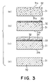
- a single-crystal silicon substrate 31 is prepared at first.
- the silicon substrate 31 has an upper or principal surface 31a and a lower or opposite surface 31b opposite to the principal surface 31a and includes a particular area, namely, a circuit element forming area adjacent to the principal surface 31a for being formed with the circuit element in the manner known in the art. It will be assumed that contaminants such as 32, such as heavy metal, are existent in the silicon substrate 31.
- the principal surface 31a of the silicon substrate 31 is oxidized to produce an oxidation film 33 as illustrated in a sectional view labelled (b).
- the oxidation film 33 has a thickness of about 400 angstroms.
- wet oxidation is carried out at 950°C to form the oxidation film 33.
- a polycrystalline silicon film 34 is deposited on the oxidation film 33 to have a thickness of, for example, 4000 angstroms.
- deposition is carried out at a temperature of 650°C under a pressure of 1 torr by the use of a silane gas. The flow rate of about 500sccm is sufficient.
- the polycrystalline silicon film 34 is subjected to phosphorus diffusion at 850°C for 60 minutes.
- the contaminants 32 are mainly concentrated around the interface between the polycrystalline silicon film 34 and the oxidation film 33, as illustrated in a sectional view labelled (c).
- the silicon substrate 31 is deleted with the polycrystalline silicon film 34 and the oxidation film 33 through a wet etching process known in the art.
- the silicon substrate 31 is formed with the circuit element in the manner known in the art.
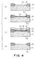
- FIG. 4 the description will be directed to a semiconductor device manufacturing method according to a second embodiment of this invention. Similar parts are designated by like reference numerals.
- isolation oxidation films such as 36 known in the art.
- Each of the isolation oxidation films 36 will be referred to as a selective oxidation film and is formed on or in a part of the principal surface 31a of the silicon substrate 31 to have a thickness of, for example, 6000 angstroms.
- the silicon substrate 31 is oxidized to form the oxidation film 33 as illustrated in a sectional view labelled (b). Thereafter, the polycrystalline silicon film 34 is deposited on the oxidation film 33 and then subjected to phosphorus diffusion as illustrated in a sectional view labelled (c).
- the presence of the isolation oxidation films 36 provides an unevenness on the upper surface of the silicon substrate 31. This gives rise to further stress concentration so as to facilitate accumulation of the contaminants 32. Heavy metal contaminants 32' readily concentrate to an edge portion of the isolation oxidation film 36. In particular, Fe tends to concentrate on such an oxidation film.
- the use of the polycrystalline silicon film 34 provides a greater effect in removal of the contaminants than that attained in the above-mentioned method described with reference to Fig. 3.
- the polycrystalline silicon film 34 is formed on the oxidation film 33 so that the contaminants 32 in the semiconductor substrate 31 are trapped in the interface between the oxidation film 33 and the polycrystalline silicon film 34. As compared with the case of the oxidation film alone, a greater amount of the contaminants 32 can be trapped.
- Fig. 5 the description will be directed to a semiconductor device manufacturing method according to a third embodiment of this invention. Similar parts are designated by like reference numerals.
- the silicon substrate 31 contains the contaminants 32 such as iron and that the contaminants present on the principal surface 31 and the particular area of the silicon substrate 31.
- the principal surface of the silicon substrate 31 is oxidized to produce the oxidation film 33 as illustrated in a sectional view labelled (b).
- the oxidation film 33 has a thickness of, for example, about 400 angstroms.
- the polycrystalline silicon film 34 is deposited on the oxidation film 33 to have a thickness of, for example, 4000 angstroms.
- deposition is carried out at a temperature of 650°C under a pressure of 1 torr by the use of silane gas. The flow rate of about 500sccm is sufficient.
- the polycrystalline silicon film 34 is subjected to phosphorus diffusion at a temperature of 820°C for 60 minutes. As a consequence, the contaminants 32 are mainly concentrated around the interface between the polycrystalline silicon film 34 and the oxidation film 33, as illustrated in a sectional view labelled (c).
- oxygen atoms 37 are present within the silicon substrate 31.
- a high-temperature heat treatment is carried out, for example, at 1200°C for four hours.
- the oxygen atoms 37 are outwardly diffused from the particular area of the silicon substrate 31 as shown by arrow marks such as 38 in a sectional view labelled (d).
- the oxygen atoms 37 are reduced from the silicon substrate 31.
- the particular area will be called hereafter a low oxygen concentration area 39.
- the low oxygen concentration area 39 does not substantially include the oxygen atoms 37 and may include a small number of the contaminants 32.
- a heat treatment is carried out, for example, at 1000°C for eight hours.
- the oxygen atoms 37 are precipitated as oxygen precipitations such as 41 in the silicon substrate 31.
- the contaminants 32 remaining in the silicon substrate 31 can be trapped in each of the oxygen precipitations 41 as illustrated in a sectional view labelled (e).
- the oxygen precipitations 41 are not produced in the low oxygen concentration area 39. Accordingly, the contaminants 32 can be excluded from the particular area, or the circuit element forming area.
- the polycrystalline silicon film 34 and the oxidation film 33 are deleted through the wet etching process as illustrated in a sectional view labelled (f).
- the contaminants 32 can be removed from the silicon substrate 31 together with the polycrystalline silicon film 34 and the oxidation film 33.
- removal of the polycrystalline silicon film 34 and the oxidation film 33 is carried out after completion of an intrinsic gettering process known in the art.
- the removal of the films 34 and 33 may be carried out before or during the heat treatment.
- Fig. 6 the description will be directed to a semiconductor device manufacturing method according to a fourth embodiment of this invention. Similar parts are designated by like reference numerals. The description is omitted as regards sectional views labelled (a) through (d). This is because the description as regards those sectional views are similar to that in the method described above with reference to Fig. 5.
- the low oxygen concentration area 39 After forming the low oxygen concentration area 39 as illustrated in a sectional view labelled (d), an additional step is incorporated where a low-temperature heat treatment is carried out at a temperature between 600°C and 800°C. As a result, nuclei are precipitated as precipitation nuclei such as 42 as illustrated in a sectional view labelled (e).
- the low oxygen concentration area 39 has a depth of about 50 ⁇ m from the surface of the silicon substrate 31.
- a heat treatment is carried out as the low-temperature heat treatment at 700°C for 16 hours.
- the precipitation nuclei 42 are formed at a relatively deep position of the silicon substrate 31.
- another heat treatment is carried out at 1000°C for eight hours to produce the oxygen precipitations 41 as illustrated in a sectional view labelled (f).
- the oxygen depositions 41 are not produced in the low oxygen concentration area 39. Accordingly, the contaminants 32 is trapped in the oxygen precipitations 41 and are also excluded from the low oxygen concentration area 39, namely, the area within 50 ⁇ m from the surface of the silicon substrate 31.
- the polycrystalline silicon film 34 and the oxidation film 33 are deleted through the wet etching process as illustrated in a sectional view labelled (g).
- the contaminants trapped in the polycrystalline silicon film 34 and the oxidation film 33 can be eliminated from the silicon substrate 31.
- the polycrystalline silicon film 34 and the oxidation film 33 may be deleted before or during the intrinsic gettering process.
- FIG. 7 the description will be directed to a semiconductor device manufacturing method according to a fifth embodiment of this invention. Similar parts are designated by like reference numerals.
- the silicon substrate 31 is prepared at first. It is assumed that the silicon substrate 31 contains the oxygen atoms 37.
- the silicon substrate 31 As regards the silicon substrate 31, a heat treatment is carried out, for example, at 1200°C for four hours. In this event, the oxygen atoms 37 are outwardly diffused from the particular area of the silicon substrate 31 through the principal surface 31a as shown by arrow marks such as 43 in a sectional view labelled (b). As a result, the low oxygen concentration area 39 is produced to have a depth of about 500 angstroms from the particular surface 31a of the silicon substrate 31.
- the oxygen precipitations 41 are produced in the silicon substrate 31 as illustrated in a sectional view labelled (c).
- the oxygen precipitations 41 are not produced in the low oxygen concentration area 39 but is produced only in a relatively deep portion of the silicon substrate 31. It is to be noted that the relatively deep portion is sufficiently spaced from the principal surface 31a of the silicon substrate 31.
- the oxidation film 33 has a thickness of, for example, about 400 angstroms. In this event, the contaminants 32 are partly trapped in the oxidation film 33, in the interface between the oxidation film 33 and the silicon substrate 31, and in the oxygen precipitations 41.
- the polycrystalline silicon film 34 is deposited on the oxidation film 33 to have a thickness of, for example, 4000 angstroms. Deposition is carried out, for example, at a temperature of 650°C under a pressure of 1 torr by the use of silane gas. The flow rate of about 500sccm is sufficient. Furthermore, the polycrystalline silicon film 34 is subjected to phosphorus diffusion at 820°C for 60 minutes. As a consequence, the contaminants 32 concentrate around the interface between the polycrystalline silicon film 34 and the oxidation film 33 as well as in the oxygen precipitations 41 present in the silicon substrate 31, as illustrated in a sectional view labelled (f).
- the polycrystalline silicon film 34 and the oxidation film 33 are deleted through the wet etching process.
- the contaminants 32 are eliminated from the silicon substrate 31 together with the polycrystalline silicon film 34 and the oxidation film 33 as illustrated in a sectional view labelled (g).
- the oxygen precipitations 41 are present only in the relatively deep portion that is sufficiently spaced from the circuit element forming area. Accordingly, it is possible to eliminate the contaminants 32 and the crystal defects such as the oxygen precipitations 41 from the circuit element forming area.
- FIG. 8 the description will be directed to a semiconductor device manufacturing method according to a sixth embodiment of this invention. Similar parts are designated by like reference numerals.
- the silicon substrate 31 is prepared at first. It is assumed that the silicon substrate 31 contains the oxygen atoms 37.
- the silicon substrate 31 As regards the silicon substrate 31, a heat treatment is carried out, for example, at 1200°C for four hours. In this event, the oxygen atoms 37 are outwardly diffused from the particular area of the silicon substrate 31 through the principal surface 31a as shown by the arrow marks 43 in a sectional view labelled (b). As a result, the low oxygen concentration area 39 is produced to have a depth of about 50 ⁇ m from the principal surface 31a of the silicon substrate 31.
- the oxidation film 33 has a thickness of, for example, about 400 angstroms.
- the contaminants 32 are partly trapped in the oxidation film 33, in the interface between the oxidation film 33 and the silicon substrate 31, and in the oxygen precipitations 41 as illustrated in a sectional view labelled (f).
- the polycrystalline silicon film 34 is deposited on the oxidation film 33 to have a thickness of, for example, 4000 angstroms. Deposition is carried out, for example, at a temperature of 650°C under a pressure of 1 torr by the use of silane gas. The flow rate of about 500sccm is sufficient. Furthermore, the polycrystalline silicon film 34 is subjected to phosphorus diffusion at 820°C for 60 minutes. As a consequence, the contaminants 32 concentrate around the interface between the polycrystalline silicon film 34 and the oxidation film 33 as well as in the oxygen precipitations 41 present in the silicon substrate 31.
- the polycrystalline silicon film 34 and the oxidation film 33 are deleted through the wet etching process.
- the contaminants 32 are eliminated from the silicon substrate 31 together with the polycrystalline silicon film 34 and the oxidation film 33 as illustrated in a sectional view labelled (g).
- the oxygen precipitations 41 are present only in the relatively deep portion that is sufficiently spaced from the circuit element forming area. Accordingly, it is possible to eliminate the contaminants 32 and the crystal defects such as the oxygen precipitations 41 from the circuit element forming area.
- the heat treatment is carried out at a relatively low temperature between 600°C and 800°C to produce the precipitation nuclei 42.
- the oxygen precipitations 41 can be produced with an improved controllability. It is therefore possible to effectively reduce the contaminants 32 and the crystal defects such as the oxygen precipitations 41 in the circuit element forming area.
- the polycrystalline silicon film 34 is formed on the oxidation film 33 so that the contaminants 32 can be trapped from the silicon substrate 31 in the interface between the oxidation film 33 and the polycrystalline silicon film 34. Accordingly, as compared with the case of the oxidation film 33 alone, a greater amount of the contaminants 32 can be trapped.
- the oxygen precipitations 41 can be eliminated from the circuit element forming area of the silicon substrate 31.
- the contaminants 32 present in the relatively deep portion of the silicon substrate 31 are removed also and trapped outside of the circuit element forming area.
- a greater effect is obtained. It is also possible to reduce the contaminants 32 trapped in the oxygen precipitations 41 and remaining in the circuit element forming area.
- FIG. 9 the description will be directed to a semiconductor device manufacturing method according to a seventh embodiment of this invention. Similar parts are designated by like reference numerals.
- the silicon substrate 31 is obtained from single-crystal silicon ingot through cutting, grinding, and etching processes in the manner known in the art.
- the opposite surface 31b is given a sandblast damage 44 as illustrated in a sectional view labelled (b).
- the silicon substrate 31 is heated and insulated at 600°C in an Ar gas atmosphere.
- An excimer laser beam is emitted from a laser source of XeCl (xenon chloride) and irradiated onto the sandblast damage 44 at a laser energy density of 0.2 J/cm2 pulse.
- the silicon substrate 31 has a portion which is melted to have a depth of 0.2 ⁇ m and to form a laser-annealed layer 45 as illustrated in a sectional view labelled (c).
- the silicon substrate 31 is cooled down to a decreased temperature.
- the principal surface 31a of the silicon substrate 31 is polished into a mirror surface.
- the silicon substrate 31 contains the contaminants 32 in the silicon substrate 31.
- An example of distribution of the contaminants 32 is illustrated in a sectional view labelled (d).
- the silicon substrate 31 is subjected to thermal oxidation.
- the principal and the opposite surfaces 31a and 31b of the silicon substrate 31 are oxidized to form the oxidation films 33 as illustrated in a sectional view labelled (e).
- the polycrystalline silicon films 34 are deposited on the oxidation films 33 as illustrated in a sectional view labelled (f). Then, the polycrystalline silicon films 34 are subjected to phosphorus diffusion. The contaminants 32 concentrate around the interface between each of the polycrystalline silicon films 34 and each of the oxidation films 33, in the laser-annealed layer 45, and in the sandblast damage 44.
- the polycrystalline silicon film 34 and the oxidation film 33 are deleted by the wet etching process as illustrated in a sectional view labelled (g).
- the contaminants 32 are eliminated from the silicon substrate 31 together with the polycrystalline silicon film 34 and the oxidation film 33.
- the extrinsic gettering is carried out by the use of the sandblasting technique and the laser damaging method.
- use may be made of other backside damaging methods, ion implantation methods of carrying out ion implantation in the opposite surface to damage a crystal lattice, or methods of excessively diffusing a dopant in the opposite surface to deform the crystal lattice.
- a yet greater effect is obtained by incorporating an additional step of eliminating the oxygen precipitations 41 in the vicinity of each of the principal and the opposite surfaces.
- a heat treatment for intrinsic gettering is carried out which is composed of a combination of a high-temperature heat treatment at a temperature not lower than 1100°C and a low-temperature heat treatment at a temperature not higher than 800°C.
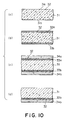
- Fig. 10 the description will be directed to a semiconductor device manufacturing method according to an eighth embodiment of this invention. Similar parts are designated by like reference numerals.
- the silicon substrate 31 contains the contaminants 32 in the silicon substrate 31.
- the principal and the opposite surfaces 31a and 31b of the silicon substrate 31 is oxidized to form upper and lower oxidation films 33a and 33b as illustrated in a sectional view labelled (b).
- upper and lower polycrystalline silicon films 34a and 34b are deposited on the upper and the lower oxidation films 33a and 33b, respectively.
- the upper and the lower polycrystalline silicon films 34a and 34b are subjected to phosphorus diffusion.
- a protection film (not shown) is formed only on the lower polycrystalline silicon film 34b.
- the upper polycrystalline silicon film 34a and the upper oxidation film 33a are subjected to the wet etching process.
- the upper polycrystalline silicon film 34a and the upper oxidation film 33a are exclusively deleted only from the circuit element forming surface illustrated in a sectional view labelled (d).
- the contaminants 32 present in a device activation area of the silicon substrate 31 are removed also.
- the lower polycrystalline silicon film 34b and the lower oxidation film 33b are left at a bottom side of the silicon substrate 31.
- the contaminants 32 are eliminated from the device activation area. In this event, the effect of removal of the contaminants 32 is continued in the subsequent steps after removal of the upper polycrystalline silicon film 34 and the upper oxidation film 33.
- the upper and the lower polycrystalline silicon films 34a and 34b are formed on the upper and the lower oxidation films 33a and 33b so that the contaminants 32 can be trapped from the silicon substrate 31 in the interface between each of the upper and the lower oxidation films 33a and 33b and the upper and the lower polycrystalline silicon films 34a and 34b.
- the oxidation film alone a greater amount of the contaminants 32 can be trapped and eliminated from the device activation area.
Landscapes
- Formation Of Insulating Films (AREA)
- Element Separation (AREA)
- Cleaning Or Drying Semiconductors (AREA)
Applications Claiming Priority (2)
| Application Number | Priority Date | Filing Date | Title |
|---|---|---|---|
| JP347134/92 | 1992-12-25 | ||
| JP4347134A JP3024409B2 (ja) | 1992-12-25 | 1992-12-25 | 半導体装置の製造方法 |
Related Child Applications (1)
| Application Number | Title | Priority Date | Filing Date |
|---|---|---|---|
| EP98200739 Division | 1998-03-09 |
Publications (3)
| Publication Number | Publication Date |
|---|---|
| EP0604234A2 true EP0604234A2 (de) | 1994-06-29 |
| EP0604234A3 EP0604234A3 (de) | 1995-01-11 |
| EP0604234B1 EP0604234B1 (de) | 1999-03-17 |
Family
ID=18388144
Family Applications (1)
| Application Number | Title | Priority Date | Filing Date |
|---|---|---|---|
| EP93310507A Expired - Lifetime EP0604234B1 (de) | 1992-12-25 | 1993-12-23 | Verfahren zur Herstellung einer Halbleitervorrichtung |
Country Status (5)
| Country | Link |
|---|---|
| US (1) | US5444001A (de) |
| EP (1) | EP0604234B1 (de) |
| JP (1) | JP3024409B2 (de) |
| KR (1) | KR0136742B1 (de) |
| DE (1) | DE69323979T2 (de) |
Cited By (7)
| Publication number | Priority date | Publication date | Assignee | Title |
|---|---|---|---|---|
| EP0635879A3 (de) * | 1993-07-22 | 1996-10-23 | Toshiba Kk | Silizium-Halbleiterplättchen und Verfahren zur Herstellung. |
| EP0822588A3 (de) * | 1996-08-01 | 1998-02-25 | Siemens Aktiengesellschaft | Dotiertes Siliziumsubstrat |
| GB2368464A (en) * | 1999-02-02 | 2002-05-01 | Nec Corp | Removing crystal originated particles from Czochralski silicon substrates |
| US6448157B1 (en) | 1999-02-02 | 2002-09-10 | Nec Corporation | Fabrication process for a semiconductor device |
| US6562733B2 (en) | 1997-09-30 | 2003-05-13 | Nec Corporation | Semiconductor device manufacturing method |
| DE102009051009A1 (de) | 2009-10-28 | 2011-05-05 | Siltronic Ag | Verfahren zum Polieren einer Halbleiterscheibe aus einkristallinem Silizium |
| USRE43450E1 (en) | 1994-09-29 | 2012-06-05 | Semiconductor Energy Laboratory Co., Ltd. | Method for fabricating semiconductor thin film |
Families Citing this family (18)
| Publication number | Priority date | Publication date | Assignee | Title |
|---|---|---|---|---|
| JPH06104268A (ja) * | 1992-09-21 | 1994-04-15 | Mitsubishi Electric Corp | ゲッタリング効果を持たせた半導体基板およびその製造方法 |
| US5789284A (en) * | 1994-09-29 | 1998-08-04 | Semiconductor Energy Laboratory Co., Ltd. | Method for fabricating semiconductor thin film |
| JP4559397B2 (ja) * | 1994-09-29 | 2010-10-06 | 株式会社半導体エネルギー研究所 | 結晶性珪素膜の作製方法、及び薄膜トランジスタの作製方法 |
| US5789308A (en) * | 1995-06-06 | 1998-08-04 | Advanced Micro Devices, Inc. | Manufacturing method for wafer slice starting material to optimize extrinsic gettering during semiconductor fabrication |
| JPH09120965A (ja) * | 1995-10-25 | 1997-05-06 | Toshiba Corp | 半導体装置の製造方法 |
| US6331457B1 (en) | 1997-01-24 | 2001-12-18 | Semiconductor Energy Laboratory., Ltd. Co. | Method for manufacturing a semiconductor thin film |
| JPH10209168A (ja) | 1997-01-24 | 1998-08-07 | Nec Corp | 半導体装置の製造方法 |
| US6146980A (en) * | 1997-06-04 | 2000-11-14 | United Microelectronics Corp. | Method for manufacturing silicon substrate having gettering capability |
| JP3830623B2 (ja) | 1997-07-14 | 2006-10-04 | 株式会社半導体エネルギー研究所 | 結晶性半導体膜の作製方法 |
| JP3295346B2 (ja) | 1997-07-14 | 2002-06-24 | 株式会社半導体エネルギー研究所 | 結晶性珪素膜の作製方法及びそれを用いた薄膜トランジスタ |
| US6277194B1 (en) * | 1999-10-21 | 2001-08-21 | Applied Materials, Inc. | Method for in-situ cleaning of surfaces in a substrate processing chamber |
| US6555487B1 (en) | 2000-08-31 | 2003-04-29 | Micron Technology, Inc. | Method of selective oxidation conditions for dielectric conditioning |
| JP2006190896A (ja) * | 2005-01-07 | 2006-07-20 | Renesas Technology Corp | エピタキシャルシリコンウエハとその製造方法および半導体装置とその製造方法 |
| JP5063867B2 (ja) * | 2005-04-21 | 2012-10-31 | 株式会社Sumco | Soi基板の製造方法 |
| JP2007220825A (ja) * | 2006-02-15 | 2007-08-30 | Sumco Corp | シリコンウェーハの製造方法 |
| US7737004B2 (en) * | 2006-07-03 | 2010-06-15 | Semiconductor Components Industries Llc | Multilayer gettering structure for semiconductor device and method |
| JP5752264B2 (ja) * | 2010-12-27 | 2015-07-22 | シャンハイ シングイ テクノロジー カンパニー リミテッドShanghai Simgui Technology Co., Ltd | 不純物のゲッタリングプロセスで絶縁層付きの半導体基板を製造する方法 |
| JP7047688B2 (ja) * | 2018-09-19 | 2022-04-05 | 三菱マテリアル株式会社 | 多結晶シリコンロッドの製造方法 |
Family Cites Families (16)
| Publication number | Priority date | Publication date | Assignee | Title |
|---|---|---|---|---|
| US4053335A (en) * | 1976-04-02 | 1977-10-11 | International Business Machines Corporation | Method of gettering using backside polycrystalline silicon |
| US4144099A (en) * | 1977-10-31 | 1979-03-13 | International Business Machines Corporation | High performance silicon wafer and fabrication process |
| JPS5680139A (en) * | 1979-12-05 | 1981-07-01 | Chiyou Lsi Gijutsu Kenkyu Kumiai | Manufacture of semiconductor device |
| JPS5848936A (ja) * | 1981-09-10 | 1983-03-23 | Fujitsu Ltd | 半導体装置の製造方法 |
| US4608096A (en) * | 1983-04-04 | 1986-08-26 | Monsanto Company | Gettering |
| JPS61135128A (ja) * | 1984-12-06 | 1986-06-23 | Toshiba Corp | 半導体装置の製造方法 |
| JPS61159741A (ja) * | 1984-12-31 | 1986-07-19 | Sony Corp | 半導体装置の製造方法 |
| JPS61214555A (ja) * | 1985-03-20 | 1986-09-24 | Hitachi Ltd | 半導体装置 |
| JPS6226826A (ja) * | 1985-07-26 | 1987-02-04 | Nec Corp | 半導体装置の製造方法 |
| JPS62208638A (ja) * | 1986-03-07 | 1987-09-12 | Toshiba Corp | 半導体装置の製造方法 |
| DE3910185C2 (de) * | 1988-03-30 | 1998-09-24 | Nippon Steel Corp | Siliziumplättchen mit hervorragendem Gettervermögen und Verfahren zu dessen Herstellung |
| JPH0648686B2 (ja) * | 1988-03-30 | 1994-06-22 | 新日本製鐵株式会社 | ゲッタリング能力の優れたシリコンウェーハおよびその製造方法 |
| US5189508A (en) * | 1988-03-30 | 1993-02-23 | Nippon Steel Corporation | Silicon wafer excelling in gettering ability and method for production thereof |
| JPH01298726A (ja) * | 1988-05-27 | 1989-12-01 | Hitachi Ltd | 半導体ウエハの製造方法およびその半導体ウエハを用いた半導体装置 |
| JPH03154346A (ja) * | 1989-11-13 | 1991-07-02 | Fujitsu Ltd | ゲッタリング方法 |
| JPH0472735A (ja) * | 1990-07-13 | 1992-03-06 | Mitsubishi Materials Corp | 半導体ウエーハのゲッタリング方法 |
-
1992
- 1992-12-25 JP JP4347134A patent/JP3024409B2/ja not_active Expired - Lifetime
-
1993
- 1993-12-23 US US08/172,248 patent/US5444001A/en not_active Expired - Fee Related
- 1993-12-23 DE DE69323979T patent/DE69323979T2/de not_active Expired - Fee Related
- 1993-12-23 EP EP93310507A patent/EP0604234B1/de not_active Expired - Lifetime
- 1993-12-24 KR KR1019930030165A patent/KR0136742B1/ko not_active Expired - Fee Related
Cited By (9)
| Publication number | Priority date | Publication date | Assignee | Title |
|---|---|---|---|---|
| EP0635879A3 (de) * | 1993-07-22 | 1996-10-23 | Toshiba Kk | Silizium-Halbleiterplättchen und Verfahren zur Herstellung. |
| US5738942A (en) * | 1993-07-22 | 1998-04-14 | Kabushiki Kaisha Toshiba | Semiconductor silicon wafer and process for producing it |
| USRE43450E1 (en) | 1994-09-29 | 2012-06-05 | Semiconductor Energy Laboratory Co., Ltd. | Method for fabricating semiconductor thin film |
| EP0822588A3 (de) * | 1996-08-01 | 1998-02-25 | Siemens Aktiengesellschaft | Dotiertes Siliziumsubstrat |
| US6562733B2 (en) | 1997-09-30 | 2003-05-13 | Nec Corporation | Semiconductor device manufacturing method |
| GB2368464A (en) * | 1999-02-02 | 2002-05-01 | Nec Corp | Removing crystal originated particles from Czochralski silicon substrates |
| US6448157B1 (en) | 1999-02-02 | 2002-09-10 | Nec Corporation | Fabrication process for a semiconductor device |
| GB2368464B (en) * | 1999-02-02 | 2002-10-16 | Nec Corp | Semiconductor device and fabrication process therefor |
| DE102009051009A1 (de) | 2009-10-28 | 2011-05-05 | Siltronic Ag | Verfahren zum Polieren einer Halbleiterscheibe aus einkristallinem Silizium |
Also Published As
| Publication number | Publication date |
|---|---|
| DE69323979T2 (de) | 1999-07-29 |
| EP0604234A3 (de) | 1995-01-11 |
| JPH06196490A (ja) | 1994-07-15 |
| EP0604234B1 (de) | 1999-03-17 |
| KR0136742B1 (ko) | 1998-04-29 |
| DE69323979D1 (de) | 1999-04-22 |
| JP3024409B2 (ja) | 2000-03-21 |
| US5444001A (en) | 1995-08-22 |
Similar Documents
| Publication | Publication Date | Title |
|---|---|---|
| US5444001A (en) | Method of manufacturing a semiconductor device readily capable of removing contaminants from a silicon substrate | |
| US6593173B1 (en) | Low defect density, thin-layer, SOI substrates | |
| EP0635879A2 (de) | Silizium-Halbleiterplättchen und Verfahren zur Herstellung | |
| EP1032027A2 (de) | Verfahren zur Bildung von einem verbundenem Substrat mit einem planaren Eigengetterungsgebiet und dadurch hergestelltes Substrat | |
| US6315826B1 (en) | Semiconductor substrate and method of manufacturing the same | |
| EP1137069A1 (de) | Herstellungsverfahren für geklebten soi-wafer, und geklebter soi-wafer | |
| US20080044669A1 (en) | Method for Manufacturing Simox Substrate and Simox Substrate Obtained by the Method | |
| US7582540B2 (en) | Method for manufacturing SOI wafer | |
| US4878988A (en) | Gettering process for semiconductor wafers | |
| US5130260A (en) | Method of gettering unintentional mobile impurities in silicon wafer by using a damaged layer exposed to the reverse surface thereof | |
| JPH0582525A (ja) | Simox基板及びその製造方法 | |
| US20040053513A1 (en) | Method for production of semiconductor components | |
| US20010015466A1 (en) | Semiconductor device and method for producing same | |
| JPH08293589A (ja) | 半導体基板および半導体装置 | |
| US6171966B1 (en) | Delineation pattern for epitaxial depositions | |
| JP2734034B2 (ja) | シリコン半導体基板の処理方法 | |
| JPH0832037A (ja) | 半導体基板の作製方法 | |
| JPH0613390A (ja) | 半導体装置の製造方法 | |
| JPH05235006A (ja) | エピタキシャルウエハの形成方法 | |
| JPH0247836A (ja) | 半導体装置の製造方法 | |
| JP3024193B2 (ja) | 半導体基板の製造方法 | |
| JPH0453140A (ja) | シリコン単結晶ウエハの処理方法 | |
| JPS63253632A (ja) | 半導体基板の製造方法 | |
| US5635414A (en) | Low cost method of fabricating shallow junction, Schottky semiconductor devices | |
| KR20070022285A (ko) | Simox 기판의 제조방법 및 그 방법에 의해 얻어지는simox 기판 |
Legal Events
| Date | Code | Title | Description |
|---|---|---|---|
| PUAI | Public reference made under article 153(3) epc to a published international application that has entered the european phase |
Free format text: ORIGINAL CODE: 0009012 |
|
| AK | Designated contracting states |
Kind code of ref document: A2 Designated state(s): DE FR GB IT NL |
|
| PUAL | Search report despatched |
Free format text: ORIGINAL CODE: 0009013 |
|
| AK | Designated contracting states |
Kind code of ref document: A3 Designated state(s): DE FR GB IT NL |
|
| RHK1 | Main classification (correction) |
Ipc: H01L 21/308 |
|
| 17P | Request for examination filed |
Effective date: 19941222 |
|
| 17Q | First examination report despatched |
Effective date: 19960507 |
|
| GRAG | Despatch of communication of intention to grant |
Free format text: ORIGINAL CODE: EPIDOS AGRA |
|
| GRAG | Despatch of communication of intention to grant |
Free format text: ORIGINAL CODE: EPIDOS AGRA |
|
| GRAH | Despatch of communication of intention to grant a patent |
Free format text: ORIGINAL CODE: EPIDOS IGRA |
|
| GRAH | Despatch of communication of intention to grant a patent |
Free format text: ORIGINAL CODE: EPIDOS IGRA |
|
| GRAA | (expected) grant |
Free format text: ORIGINAL CODE: 0009210 |
|
| RIN1 | Information on inventor provided before grant (corrected) |
Inventor name: TOKUYAMA, MICHIKO, C/O NEC CORPORATION |
|
| AK | Designated contracting states |
Kind code of ref document: B1 Designated state(s): DE FR GB IT NL |
|
| REF | Corresponds to: |
Ref document number: 69323979 Country of ref document: DE Date of ref document: 19990422 |
|
| ET | Fr: translation filed | ||
| PLBE | No opposition filed within time limit |
Free format text: ORIGINAL CODE: 0009261 |
|
| STAA | Information on the status of an ep patent application or granted ep patent |
Free format text: STATUS: NO OPPOSITION FILED WITHIN TIME LIMIT |
|
| 26N | No opposition filed | ||
| PGFP | Annual fee paid to national office [announced via postgrant information from national office to epo] |
Ref country code: FR Payment date: 20011212 Year of fee payment: 9 |
|
| PGFP | Annual fee paid to national office [announced via postgrant information from national office to epo] |
Ref country code: GB Payment date: 20011227 Year of fee payment: 9 |
|
| PGFP | Annual fee paid to national office [announced via postgrant information from national office to epo] |
Ref country code: NL Payment date: 20011228 Year of fee payment: 9 |
|
| REG | Reference to a national code |
Ref country code: GB Ref legal event code: IF02 |
|
| PGFP | Annual fee paid to national office [announced via postgrant information from national office to epo] |
Ref country code: DE Payment date: 20020109 Year of fee payment: 9 |
|
| PG25 | Lapsed in a contracting state [announced via postgrant information from national office to epo] |
Ref country code: GB Free format text: LAPSE BECAUSE OF NON-PAYMENT OF DUE FEES Effective date: 20021223 |
|
| PG25 | Lapsed in a contracting state [announced via postgrant information from national office to epo] |
Ref country code: NL Free format text: LAPSE BECAUSE OF NON-PAYMENT OF DUE FEES Effective date: 20030701 Ref country code: DE Free format text: LAPSE BECAUSE OF NON-PAYMENT OF DUE FEES Effective date: 20030701 |
|
| GBPC | Gb: european patent ceased through non-payment of renewal fee |
Effective date: 20021223 |
|
| NLV4 | Nl: lapsed or anulled due to non-payment of the annual fee |
Effective date: 20030701 |
|
| PG25 | Lapsed in a contracting state [announced via postgrant information from national office to epo] |
Ref country code: FR Free format text: LAPSE BECAUSE OF NON-PAYMENT OF DUE FEES Effective date: 20030901 |
|
| REG | Reference to a national code |
Ref country code: FR Ref legal event code: ST |
|
| PG25 | Lapsed in a contracting state [announced via postgrant information from national office to epo] |
Ref country code: IT Free format text: LAPSE BECAUSE OF NON-PAYMENT OF DUE FEES Effective date: 20051223 |