EP0735593A1 - MESFET mit versenktem Gate und Herstellungsverfahren - Google Patents
MESFET mit versenktem Gate und Herstellungsverfahren Download PDFInfo
- Publication number
- EP0735593A1 EP0735593A1 EP96105083A EP96105083A EP0735593A1 EP 0735593 A1 EP0735593 A1 EP 0735593A1 EP 96105083 A EP96105083 A EP 96105083A EP 96105083 A EP96105083 A EP 96105083A EP 0735593 A1 EP0735593 A1 EP 0735593A1
- Authority
- EP
- European Patent Office
- Prior art keywords
- recess
- active layer
- field effect
- semiconductor device
- coating
- Prior art date
- Legal status (The legal status is an assumption and is not a legal conclusion. Google has not performed a legal analysis and makes no representation as to the accuracy of the status listed.)
- Withdrawn
Links
- 238000004519 manufacturing process Methods 0.000 title description 17
- 230000005669 field effect Effects 0.000 claims abstract description 60
- 239000004065 semiconductor Substances 0.000 claims abstract description 58
- 238000000034 method Methods 0.000 claims description 36
- 239000011248 coating agent Substances 0.000 claims description 30
- 238000000576 coating method Methods 0.000 claims description 30
- 238000005530 etching Methods 0.000 claims description 19
- 239000000463 material Substances 0.000 claims description 12
- 238000007789 sealing Methods 0.000 claims description 4
- 229920002120 photoresistant polymer Polymers 0.000 description 37
- 230000015556 catabolic process Effects 0.000 description 18
- 239000000758 substrate Substances 0.000 description 18
- 229910001218 Gallium arsenide Inorganic materials 0.000 description 13
- 230000005684 electric field Effects 0.000 description 12
- 239000002184 metal Substances 0.000 description 12
- 229910052751 metal Inorganic materials 0.000 description 12
- 238000009413 insulation Methods 0.000 description 8
- 238000000206 photolithography Methods 0.000 description 6
- NBIIXXVUZAFLBC-UHFFFAOYSA-N Phosphoric acid Chemical compound OP(O)(O)=O NBIIXXVUZAFLBC-UHFFFAOYSA-N 0.000 description 4
- 239000012535 impurity Substances 0.000 description 3
- 150000002500 ions Chemical class 0.000 description 3
- 230000004807 localization Effects 0.000 description 3
- 230000002411 adverse Effects 0.000 description 2
- 229910000147 aluminium phosphate Inorganic materials 0.000 description 2
- 230000003247 decreasing effect Effects 0.000 description 2
- 238000001451 molecular beam epitaxy Methods 0.000 description 2
- MYMOFIZGZYHOMD-UHFFFAOYSA-N Dioxygen Chemical compound O=O MYMOFIZGZYHOMD-UHFFFAOYSA-N 0.000 description 1
- 229910000530 Gallium indium arsenide Inorganic materials 0.000 description 1
- 229910052782 aluminium Inorganic materials 0.000 description 1
- 230000015572 biosynthetic process Effects 0.000 description 1
- 230000000593 degrading effect Effects 0.000 description 1
- 238000000151 deposition Methods 0.000 description 1
- 229910001882 dioxygen Inorganic materials 0.000 description 1
- 238000006073 displacement reaction Methods 0.000 description 1
- 238000001312 dry etching Methods 0.000 description 1
- 239000007772 electrode material Substances 0.000 description 1
- 238000001704 evaporation Methods 0.000 description 1
- 239000012467 final product Substances 0.000 description 1
- 229910052737 gold Inorganic materials 0.000 description 1
- 238000012544 monitoring process Methods 0.000 description 1
- 238000002161 passivation Methods 0.000 description 1
- 229910052697 platinum Inorganic materials 0.000 description 1
- 229910052719 titanium Inorganic materials 0.000 description 1
- 238000001039 wet etching Methods 0.000 description 1
Images



Classifications
-
- H—ELECTRICITY
- H10—SEMICONDUCTOR DEVICES; ELECTRIC SOLID-STATE DEVICES NOT OTHERWISE PROVIDED FOR
- H10D—INORGANIC ELECTRIC SEMICONDUCTOR DEVICES
- H10D30/00—Field-effect transistors [FET]
- H10D30/01—Manufacture or treatment
- H10D30/061—Manufacture or treatment of FETs having Schottky gates
- H10D30/0612—Manufacture or treatment of FETs having Schottky gates of lateral single-gate Schottky FETs
-
- H—ELECTRICITY
- H10—SEMICONDUCTOR DEVICES; ELECTRIC SOLID-STATE DEVICES NOT OTHERWISE PROVIDED FOR
- H10D—INORGANIC ELECTRIC SEMICONDUCTOR DEVICES
- H10D64/00—Electrodes of devices having potential barriers
- H10D64/20—Electrodes characterised by their shapes, relative sizes or dispositions
- H10D64/27—Electrodes not carrying the current to be rectified, amplified, oscillated or switched, e.g. gates
- H10D64/311—Gate electrodes for field-effect devices
- H10D64/411—Gate electrodes for field-effect devices for FETs
- H10D64/511—Gate electrodes for field-effect devices for FETs for IGFETs
- H10D64/512—Disposition of the gate electrodes, e.g. buried gates
- H10D64/513—Disposition of the gate electrodes, e.g. buried gates within recesses in the substrate, e.g. trench gates, groove gates or buried gates
-
- H—ELECTRICITY
- H10—SEMICONDUCTOR DEVICES; ELECTRIC SOLID-STATE DEVICES NOT OTHERWISE PROVIDED FOR
- H10D—INORGANIC ELECTRIC SEMICONDUCTOR DEVICES
- H10D12/00—Bipolar devices controlled by the field effect, e.g. insulated-gate bipolar transistors [IGBT]
- H10D12/01—Manufacture or treatment
- H10D12/031—Manufacture or treatment of IGBTs
- H10D12/032—Manufacture or treatment of IGBTs of vertical IGBTs
- H10D12/038—Manufacture or treatment of IGBTs of vertical IGBTs having a recessed gate, e.g. trench-gate IGBTs
-
- H—ELECTRICITY
- H10—SEMICONDUCTOR DEVICES; ELECTRIC SOLID-STATE DEVICES NOT OTHERWISE PROVIDED FOR
- H10D—INORGANIC ELECTRIC SEMICONDUCTOR DEVICES
- H10D30/00—Field-effect transistors [FET]
- H10D30/80—FETs having rectifying junction gate electrodes
- H10D30/87—FETs having Schottky gate electrodes, e.g. metal-semiconductor FETs [MESFET]
- H10D30/873—FETs having Schottky gate electrodes, e.g. metal-semiconductor FETs [MESFET] having multiple gate electrodes
-
- H—ELECTRICITY
- H10—SEMICONDUCTOR DEVICES; ELECTRIC SOLID-STATE DEVICES NOT OTHERWISE PROVIDED FOR
- H10D—INORGANIC ELECTRIC SEMICONDUCTOR DEVICES
- H10D30/00—Field-effect transistors [FET]
- H10D30/80—FETs having rectifying junction gate electrodes
- H10D30/87—FETs having Schottky gate electrodes, e.g. metal-semiconductor FETs [MESFET]
- H10D30/877—FETs having Schottky gate electrodes, e.g. metal-semiconductor FETs [MESFET] having recessed gate electrodes
-
- H—ELECTRICITY
- H10—SEMICONDUCTOR DEVICES; ELECTRIC SOLID-STATE DEVICES NOT OTHERWISE PROVIDED FOR
- H10D—INORGANIC ELECTRIC SEMICONDUCTOR DEVICES
- H10D84/00—Integrated devices formed in or on semiconductor substrates that comprise only semiconducting layers, e.g. on Si wafers or on GaAs-on-Si wafers
- H10D84/01—Manufacture or treatment
- H10D84/0123—Integrating together multiple components covered by H10D12/00 or H10D30/00, e.g. integrating multiple IGBTs
- H10D84/0126—Integrating together multiple components covered by H10D12/00 or H10D30/00, e.g. integrating multiple IGBTs the components including insulated gates, e.g. IGFETs
- H10D84/013—Manufacturing their source or drain regions, e.g. silicided source or drain regions
-
- H—ELECTRICITY
- H10—SEMICONDUCTOR DEVICES; ELECTRIC SOLID-STATE DEVICES NOT OTHERWISE PROVIDED FOR
- H10D—INORGANIC ELECTRIC SEMICONDUCTOR DEVICES
- H10D84/00—Integrated devices formed in or on semiconductor substrates that comprise only semiconducting layers, e.g. on Si wafers or on GaAs-on-Si wafers
- H10D84/01—Manufacture or treatment
- H10D84/0123—Integrating together multiple components covered by H10D12/00 or H10D30/00, e.g. integrating multiple IGBTs
- H10D84/0126—Integrating together multiple components covered by H10D12/00 or H10D30/00, e.g. integrating multiple IGBTs the components including insulated gates, e.g. IGFETs
- H10D84/0135—Manufacturing their gate conductors
Definitions
- Fig. 1 is a cross-sectional view showing a field effect semiconductor device 1 according to an embodiment of the present invention.
- the field effect semiconductor device 1 includes a substrate 2.
- the substrate 2 comprises a semi-insulating GaAs layer 3 and an active layer 4 provided on the semi-insulating GaAs layer 4.
- the substrate 2 can be formed by implanting impurity ions into a surface region of the semi-insulating GaAs layer 4 or by epitaxially growing the active layer 4 on the semi-insulating GaAs layer 3 through a molecular beam epitaxy (MBE) method or the like.
- MBE molecular beam epitaxy
- Fig. 4 is a cross-sectional view showing the structure of a field effect semiconductor device 14 according to still another embodiment of the present invention.
- the metal electrode 10 is provided in the second recess 9, but no insulating film is formed over the second recess 9 and the drain electrode 6.
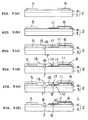
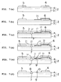
- a photoresist 15 is applied to the entire surface of the substrate 2, and a window 16 for forming a first recess 7 and a window 17 for forming a second recess 9 are simultaneously opened in the photoresist 15 by the photolithography method using a photomask. At this time, in the region in which the second recess 9 is to be formed, only the photoresist 15 is selectively etched and the insulation film 11 is not etched.
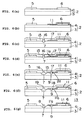
- Figs. 6(a) to 6(g) are cross-sectional views showing a fabrication method of the field effect semiconductor device 13 shown in Fig. 3.
- Figs. 6(a) to 6(e) show the same steps as the above Figs. 5(a) to 5(e).
- the photoresist 15 is removed.
- Fig. 6(f) after applying a photoresist 18 to the entire surface of the substrate 2, a window 19 for forming a gate electrode 7 in a position corresponding to the first recess 7 is formed in the photoresist 18.
- the manufacturing steps are shortened.
- the field effect semiconductor device produced by this embodiment is suitably used as a low power FET having a high breakdown voltage.
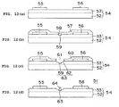
- the field effect semiconductor device could not be controlled by applying any gate bias voltage to the gate electrode in the case where the source-drain voltage is about 0V.
- the gate current I g increases as the voltage V sd increases from about 8V.
- the source-drain current I sd increases due to avalanche breakdown as the voltage V sd increases from about 9.5V.
- the g d drain conductance
Landscapes
- Junction Field-Effect Transistors (AREA)
- Electrodes Of Semiconductors (AREA)
Applications Claiming Priority (2)
| Application Number | Priority Date | Filing Date | Title |
|---|---|---|---|
| JP99535/95 | 1995-03-30 | ||
| JP7099535A JPH08274118A (ja) | 1995-03-30 | 1995-03-30 | 電界効果型半導体装置及びその製造方法 |
Publications (1)
| Publication Number | Publication Date |
|---|---|
| EP0735593A1 true EP0735593A1 (de) | 1996-10-02 |
Family
ID=14249907
Family Applications (1)
| Application Number | Title | Priority Date | Filing Date |
|---|---|---|---|
| EP96105083A Withdrawn EP0735593A1 (de) | 1995-03-30 | 1996-03-29 | MESFET mit versenktem Gate und Herstellungsverfahren |
Country Status (3)
| Country | Link |
|---|---|
| EP (1) | EP0735593A1 (de) |
| JP (1) | JPH08274118A (de) |
| KR (1) | KR960036131A (de) |
Cited By (2)
| Publication number | Priority date | Publication date | Assignee | Title |
|---|---|---|---|---|
| WO2004053996A1 (en) * | 2002-12-05 | 2004-06-24 | University Of Massachusetts Lowell | Multi-gate heterostructured field effect transistor |
| EP2040299A1 (de) * | 2007-09-12 | 2009-03-25 | Forschungsverbund Berlin e.V. | Elektronische Bauelemente mit verbesserten Transfercharakteristiken und Methode zur Optimierung der Transfercharakteristiken solcher elektronischen Bauelementen. |
Families Citing this family (3)
| Publication number | Priority date | Publication date | Assignee | Title |
|---|---|---|---|---|
| US6262444B1 (en) | 1997-04-23 | 2001-07-17 | Nec Corporation | Field-effect semiconductor device with a recess profile |
| JP2003258003A (ja) | 2002-03-06 | 2003-09-12 | Hitachi Ltd | 半導体装置及びその製造方法 |
| JP5801560B2 (ja) * | 2011-01-21 | 2015-10-28 | 株式会社豊田中央研究所 | 半導体装置 |
Citations (6)
| Publication number | Priority date | Publication date | Assignee | Title |
|---|---|---|---|---|
| JPS5752174A (en) * | 1980-09-16 | 1982-03-27 | Nec Corp | Multigate field effect transistor |
| JPH02237040A (ja) * | 1989-03-09 | 1990-09-19 | Fujitsu Ltd | 半導体装置 |
| JPH0350837A (ja) * | 1989-07-19 | 1991-03-05 | Sanyo Electric Co Ltd | 半導体素子の製造方法 |
| JPH04186845A (ja) * | 1990-11-21 | 1992-07-03 | Nec Corp | 化合物半導体装置の製造方法 |
| EP0550317A1 (de) * | 1991-12-31 | 1993-07-07 | Thomson Composants Microondes | Herstellungsverfahren für einen Hochfrequenz-Feldeffekttransistor |
| EP0664567A1 (de) * | 1994-01-25 | 1995-07-26 | Thomson-Csf Semiconducteurs Specifiques | Mikrowellenleistungstransistor mit doppelten Vertiefung und Verfahren zur Herstellung |
-
1995
- 1995-03-30 JP JP7099535A patent/JPH08274118A/ja active Pending
-
1996
- 1996-03-29 EP EP96105083A patent/EP0735593A1/de not_active Withdrawn
- 1996-03-30 KR KR1019960009593A patent/KR960036131A/ko not_active Ceased
Patent Citations (6)
| Publication number | Priority date | Publication date | Assignee | Title |
|---|---|---|---|---|
| JPS5752174A (en) * | 1980-09-16 | 1982-03-27 | Nec Corp | Multigate field effect transistor |
| JPH02237040A (ja) * | 1989-03-09 | 1990-09-19 | Fujitsu Ltd | 半導体装置 |
| JPH0350837A (ja) * | 1989-07-19 | 1991-03-05 | Sanyo Electric Co Ltd | 半導体素子の製造方法 |
| JPH04186845A (ja) * | 1990-11-21 | 1992-07-03 | Nec Corp | 化合物半導体装置の製造方法 |
| EP0550317A1 (de) * | 1991-12-31 | 1993-07-07 | Thomson Composants Microondes | Herstellungsverfahren für einen Hochfrequenz-Feldeffekttransistor |
| EP0664567A1 (de) * | 1994-01-25 | 1995-07-26 | Thomson-Csf Semiconducteurs Specifiques | Mikrowellenleistungstransistor mit doppelten Vertiefung und Verfahren zur Herstellung |
Non-Patent Citations (4)
| Title |
|---|
| PATENT ABSTRACTS OF JAPAN vol. 006, no. 123 (E - 117) 8 July 1982 (1982-07-08) * |
| PATENT ABSTRACTS OF JAPAN vol. 014, no. 550 (E - 1009) 6 December 1990 (1990-12-06) * |
| PATENT ABSTRACTS OF JAPAN vol. 016, no. 505 (E - 1281) 19 October 1992 (1992-10-19) * |
| PATENT ABSTRACTS OF JAPAN vol. 15, no. 191 (E - 1068) 16 May 1991 (1991-05-16) * |
Cited By (2)
| Publication number | Priority date | Publication date | Assignee | Title |
|---|---|---|---|---|
| WO2004053996A1 (en) * | 2002-12-05 | 2004-06-24 | University Of Massachusetts Lowell | Multi-gate heterostructured field effect transistor |
| EP2040299A1 (de) * | 2007-09-12 | 2009-03-25 | Forschungsverbund Berlin e.V. | Elektronische Bauelemente mit verbesserten Transfercharakteristiken und Methode zur Optimierung der Transfercharakteristiken solcher elektronischen Bauelementen. |
Also Published As
| Publication number | Publication date |
|---|---|
| JPH08274118A (ja) | 1996-10-18 |
| KR960036131A (ko) | 1996-10-28 |
Similar Documents
| Publication | Publication Date | Title |
|---|---|---|
| US5510280A (en) | Method of making an asymmetrical MESFET having a single sidewall spacer | |
| EP0551110B1 (de) | Verbindungshalbleiterbauelemente | |
| US5538910A (en) | Method of making a narrow gate electrode for a field effect transistor | |
| US5139968A (en) | Method of producing a t-shaped gate electrode | |
| GB2274944A (en) | Field effect transistor and method for producing the field effect transistor | |
| US5225703A (en) | Dual field effect transistor structure employing a single source region | |
| EP0735593A1 (de) | MESFET mit versenktem Gate und Herstellungsverfahren | |
| US5587328A (en) | Method for manufacturing semiconductor device | |
| GB2286720A (en) | Field effect transistors | |
| JPH02271537A (ja) | 半導体装置及びその製造方法 | |
| US5837570A (en) | Heterostructure semiconductor device and method of fabricating same | |
| US5824575A (en) | Semiconductor device and method of manufacturing the same | |
| JP3144089B2 (ja) | 電界効果トランジスタの製造方法 | |
| US20080064155A1 (en) | Method for Producing a Multi-Stage Recess in a Layer Structure and a Field Effect Transistor with a Multi-Recessed Gate | |
| JPS592385B2 (ja) | メサ型非活性Vゲ−トGaAs電界効果トランジスタとその製造方法 | |
| JP2914429B2 (ja) | 半導体集積回路の製造方法 | |
| KR100342443B1 (ko) | 전계효과 트랜지스터의 서브미크론 티이형 게이트형성방법 | |
| JPS62190772A (ja) | 電界効果トランジスタおよびその製造方法 | |
| JPS60251671A (ja) | 電界効果形トランジスタおよびその製造方法 | |
| JPS62115782A (ja) | 半導体装置の製造方法 | |
| JP3235548B2 (ja) | 半導体装置の製造方法 | |
| JP3183251B2 (ja) | 半導体装置の製造方法 | |
| JP3036451B2 (ja) | 半導体装置の製造方法 | |
| KR950000155B1 (ko) | 전계효과 트랜지스터의 제조방법 | |
| JPH0855861A (ja) | 電界効果トランジスタ、及びその製造方法 |
Legal Events
| Date | Code | Title | Description |
|---|---|---|---|
| PUAI | Public reference made under article 153(3) epc to a published international application that has entered the european phase |
Free format text: ORIGINAL CODE: 0009012 |
|
| AK | Designated contracting states |
Kind code of ref document: A1 Designated state(s): DE FI FR GB |
|
| 17P | Request for examination filed |
Effective date: 19960911 |
|
| 17Q | First examination report despatched |
Effective date: 19980128 |
|
| STAA | Information on the status of an ep patent application or granted ep patent |
Free format text: STATUS: THE APPLICATION IS DEEMED TO BE WITHDRAWN |
|
| 18D | Application deemed to be withdrawn |
Effective date: 19990225 |