EP0784865B1 - Diffundierung mit feldverstärkung und optischer aktivierung - Google Patents
Diffundierung mit feldverstärkung und optischer aktivierung Download PDFInfo
- Publication number
- EP0784865B1 EP0784865B1 EP95935183A EP95935183A EP0784865B1 EP 0784865 B1 EP0784865 B1 EP 0784865B1 EP 95935183 A EP95935183 A EP 95935183A EP 95935183 A EP95935183 A EP 95935183A EP 0784865 B1 EP0784865 B1 EP 0784865B1
- Authority
- EP
- European Patent Office
- Prior art keywords
- impurity
- diamond
- target material
- crystalline target
- type
- Prior art date
- Legal status (The legal status is an assumption and is not a legal conclusion. Google has not performed a legal analysis and makes no representation as to the accuracy of the status listed.)
- Expired - Lifetime
Links
Images

Classifications
-
- H—ELECTRICITY
- H10—SEMICONDUCTOR DEVICES; ELECTRIC SOLID-STATE DEVICES NOT OTHERWISE PROVIDED FOR
- H10D—INORGANIC ELECTRIC SEMICONDUCTOR DEVICES
- H10D48/00—Individual devices not covered by groups H10D1/00 - H10D44/00
- H10D48/01—Manufacture or treatment
- H10D48/031—Manufacture or treatment of three-or-more electrode devices
-
- H—ELECTRICITY
- H10—SEMICONDUCTOR DEVICES; ELECTRIC SOLID-STATE DEVICES NOT OTHERWISE PROVIDED FOR
- H10P—GENERIC PROCESSES OR APPARATUS FOR THE MANUFACTURE OR TREATMENT OF DEVICES COVERED BY CLASS H10
- H10P32/00—Diffusion of dopants within, into or out of wafers, substrates or parts of devices
- H10P32/10—Diffusion of dopants within, into or out of semiconductor bodies or layers
- H10P32/14—Diffusion of dopants within, into or out of semiconductor bodies or layers within a single semiconductor body or layer in a solid phase; between different semiconductor bodies or layers, both in a solid phase
-
- H—ELECTRICITY
- H01—ELECTRIC ELEMENTS
- H01J—ELECTRIC DISCHARGE TUBES OR DISCHARGE LAMPS
- H01J9/00—Apparatus or processes specially adapted for the manufacture, installation, removal, maintenance of electric discharge tubes, discharge lamps, or parts thereof; Recovery of material from discharge tubes or lamps
- H01J9/02—Manufacture of electrodes or electrode systems
- H01J9/022—Manufacture of electrodes or electrode systems of cold cathodes
-
- H—ELECTRICITY
- H10—SEMICONDUCTOR DEVICES; ELECTRIC SOLID-STATE DEVICES NOT OTHERWISE PROVIDED FOR
- H10D—INORGANIC ELECTRIC SEMICONDUCTOR DEVICES
- H10D48/00—Individual devices not covered by groups H10D1/00 - H10D44/00
- H10D48/01—Manufacture or treatment
- H10D48/021—Manufacture or treatment of two-electrode devices
-
- H—ELECTRICITY
- H10—SEMICONDUCTOR DEVICES; ELECTRIC SOLID-STATE DEVICES NOT OTHERWISE PROVIDED FOR
- H10D—INORGANIC ELECTRIC SEMICONDUCTOR DEVICES
- H10D62/00—Semiconductor bodies, or regions thereof, of devices having potential barriers
- H10D62/80—Semiconductor bodies, or regions thereof, of devices having potential barriers characterised by the materials
- H10D62/83—Semiconductor bodies, or regions thereof, of devices having potential barriers characterised by the materials being Group IV materials, e.g. B-doped Si or undoped Ge
- H10D62/8303—Diamond
-
- H—ELECTRICITY
- H10—SEMICONDUCTOR DEVICES; ELECTRIC SOLID-STATE DEVICES NOT OTHERWISE PROVIDED FOR
- H10P—GENERIC PROCESSES OR APPARATUS FOR THE MANUFACTURE OR TREATMENT OF DEVICES COVERED BY CLASS H10
- H10P32/00—Diffusion of dopants within, into or out of wafers, substrates or parts of devices
-
- H—ELECTRICITY
- H10—SEMICONDUCTOR DEVICES; ELECTRIC SOLID-STATE DEVICES NOT OTHERWISE PROVIDED FOR
- H10P—GENERIC PROCESSES OR APPARATUS FOR THE MANUFACTURE OR TREATMENT OF DEVICES COVERED BY CLASS H10
- H10P32/00—Diffusion of dopants within, into or out of wafers, substrates or parts of devices
- H10P32/10—Diffusion of dopants within, into or out of semiconductor bodies or layers
- H10P32/185—Lithium-drift diffusion
Definitions
- the following invention relates to a forced diffusion process for making semiconductor material and in particular relates to a process for doping diamond material with impurities to make N-type diamond semiconductors which may then be used in electronics (e.g., high voltage switches, integrated circuits) optics, and other applications.
- electronics e.g., high voltage switches, integrated circuits
- Diamond is one of the best insulators known, but heretofore it has been very difficult to produce diamond semiconductor material. Some success has been attained at creating P-type diamond semiconductors, but the production of N-type diamond has been largely unsuccessful.
- P-type diamond material has been made using in situ doping and ion implantation. N-type diamond has not been made by any process except for the process of the invention to be described herein. Furthermore, in situ doping and ion implantation introduce undesirable lattice defects in the diamond when P-type impurities are used.
- Forced diffusion is a method of doping semiconductor material with impurities that has been used in the past with semiconductor material such as silicon.
- semiconductor material with impurity material placed on it is first heated.
- Dopant material in the lattice is then activated by the heat (i.e., it becomes ionized).
- An electric field created by a high voltage placed across the silicon material drives the charged dopant atoms into the semiconductor lattice structure.
- Heating alone may be sufficient to ionize only shallow level impurity dopants, but the major problem with forced diffusion is to diffuse enough impurity atoms in the lattice structure to contribute to conduction.
- the number of atoms is a function of temperature and activation energy according to the Boltzmann distribution. The higher the temperature, the more that impurity ions are created which will diffuse into the lattice structure.
- the problem is that with diamond the lattice structure begins to break down into amorphous carbon or graphite when temperature levels high enough to cause ionization are reached due to metastability of the diamond phase.
- Diamond semiconductors of N-type material require high enough concentrations of dopant atoms with shallow energy levels in order to provide the requisite degree of conductivity. Thus far, diffusion doping processes have not been capable of achieving this result. Ion implantation and in situ doping have the problems associated with then that are noted above. What is needed, therefore, is a doping process for diamond material that can create N-type semiconductor material.
- a method for making semiconductor material having the features of the preamble of claim 1 is known from: "Materials Research Society Symposium Proceedings,” Vol. 339, “Diamond, SiC and Nitride Wide Bandgap Semiconductors,” Symposium San Francisco, CA., USA, April 4-8, 1994, pages 601 to 606; “Patent Abstracts of Japan,” Vol. 017, No: 475 (C-1103), August 30,1993, corresponding to JP-A-05117089; and DE-A-4331937.
- the invention is a process for malking, among other things, N-type semiconductor material and in particular diamond semiconductors using a modified forced diffusion process.
- a lithium salt such as LiClO 3 ;may be deposited atop the diamond material.
- Lithium is a good dopant to produce N-type material because theory predicts a shallow energy level of around 0.1eV.
- Photon bombardment of the diamond material is provided by a laser.
- a laser with a photon energy Ep activates the impurity atoms with the required activation energy Ea where Ep is greater than Ea. This enables the donor atoms to diffuse along the field lines to interstitial positions in the diamond lattice.
- This process may also be used for P-type impurities by changing the electric field direction because donor impurity ions are positive (N-type) and acceptor impurity ions are negative (P-type).
- the high temperature ionizes some shallow level dopants while the force created by the electric field drives the charged dopant into the target semiconductor material creating a gradient near the diamond's surface.
- the laser is directed at the migrating lithium atoms as a photon source to provide the activation energy E a . This is a far more effective method of providing activation energy than previous methods which used only heat because of the limitations inherent in heating some semiconductor target materials, particularly diamond. Also the laser optically ionizes far more impurity atoms than could previously be produced by heat alone.
- the laser because it acts locally in the target material, may be used to create zones where high concentrations of donor atoms may abound. In this way, the laser can be focused upon a certain area or can be moved to create linear strips defining doped regions.
- This process can be used to create high voltage switches, diodes and PNP and NPN transistors, P-N junctions, PIN structures, NIP structures, NIN structures, PIP structures or any other structure which, uses N-type material.
- impurities may be diffused, either on the front and back of a thin diamond plate or in a side-by-side configuration.
- the laser When the laser is used to create doping zones, it functions as a point heat source to "draw" a pattern on the impurity layer resting on the diamond while a voltage is placed across the diamond material and a second laser is used to optically ionize impurities which enter the diamond lattice.
- Another application of the forced diffusion process of the invention is the creation of a flat screen display.
- a sheet of N-type diamond material emits electrons when charged with a voltage. This property makes it practical to place luminescent phosphor material over the diamond layer which will emit light when bombarded by electrons.
- Various addressing techniques can be used to create local voltage gradients to, in effect, create pixels in the phosphor layer.
- Yet another application of the instant invention is the coloring of natural diamond.
- the diamond is placed on a substrate holder and an impurity placed on the diamond.
- the substrate is heated and the laser illuminates the diamond to ionize the impurity.
- a high voltage is placed across the diamond, and over a period of time impurities are diffused into the diamond.
- the energy of the laser must be such that Ep>Ea.
- the process will work both for impurities located at interstitial sites as well as for those substituted for carbon in the diamond lattice.
- an excimer laser may be used which provides sufficient energy to break carbon's sp3 bonds and create vacancies. In this instance impurities will diffuse into vacancies and become substitutional.
- diffusing boron into diamond using this process creates a blue colored diamond.
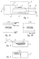
- a vacuum vessel 10 contains a substrate holder 12.
- a target chip or substrate film made from diamond 14 is deposited on the substrate holder 12.
- An impurity 16 such as a lithium salt is placed on top of the diamond 14.
- Coupled to the substrate holder 12 is a heating unit 18.
- a source of high voltage 20 has an input 22 coupled to the diamond material 14 and an output coupled to the substrate holder 12.
- the voltage unit 20 creates a voltage potential and consequently an electric field across the diamond material 14.
- a laser 26 directs a photon beam 27 at the diamond material.
- the vacuum vessel 10 is evacuated and the heating unit is turned on.
- the heater 18 may be made of graphite and ceramic heating elements and its purpose is to heat the diamond material 14 to temperatures of between room temperature and 1400°C.
- the high voltage source 20 is turned on, establishing an electric field across the diamond material 14.
- the voltage is highly variable, but experimentally, voltages of around 500 volts have produced good results.
- An acceptable laser for the process is a helium-neon laser operating at 632.8 nm which, in this configuration, provides Ep greater than Ea.
- lithium, oxygen and chlorine atoms in the impurity material 16 begin to activate (e.g., ionize in the lattice).
- these atoms begin to migrate into the crystalline lattice of the diamond material 14.
- nonionized lithium atoms also migrate into the top of the diamond film where they are bombarded by photons 27 from the laser 26. The photon bombardment provides activation energy for these atoms which in turn creates an even steeper gradient, drawing more lithium atoms into the diamond lattice structure.
- boron may be used as an acceptable impurity.
- the activation energy of the boron acceptor impurity is .3eV and it displays a work function of 5.2eV. The process is in all other respects, the same.
- FIG. 3 A variation of the process of Figure 1 is shown in Figure 3.
- the heating unit 18 is not used and a second laser 28 directs a collimated light beam 30 towards impurity material 32 deposited on a diamond substrate 34 in the vacuum vessel 10 as shown in Figure 1.
- the second laser 28 With the voltage on and the first laser 26 directed at the diamond substrate 34, the second laser 28 is moved across the impurity 32 where it functions as a point source of heat. As it heats the impurity material 32 in lines or strips, forced diffusion takes place under the influence of the electric field caused by the high voltage unit 20 and the optical ionization of migrating impurity atoms by the laser 26.
- Figure 4 The result is shown in Figure 4 in which patterned strips 36 of impurity material are "drawn" on the diamond substrate 34.
- Figures 5A and 5B show high power transistors.
- Figure 5A shows a thin diamond plate 40 which includes regions on both the front and back 42 and 44, respectively, ofN-type dopant which has diffused into the diamond material. If a voltage source 46 is placed across the diamond plate 40, the device will act as a switch.
- Figure 5B the N-type diamond materials 48 and 50 have been placed side-by-side in a thin plate of diamond material 52.
- a voltage source 54 will cause conduction between the two regions 50 and 48 depending upon the magnitude of the voltage and the lateral distance between the two regions.
- FIG. 6A Another application is shown in Figures 6A and 6B.
- P-type dopant has diffused into a plate previously doped with N-type material.
- a very thin diamond plate is used and the device will act as a diode.
- electrodes 60 and 62 are located on the same side of a P-type diamond plate 64.
- N-type material 66 is created in a region on the surface of the P-type diamond 64.
- NPN type transistors similar to those described for high voltage switches ( Figures 5A and 5B) and diodes ( Figures 6A and 6B) are shown for NPN type transistors.
- the first type of NPN transistor 66 shows a plate of P-type diamond material 68 doped with N-type material 70 and 72 respectively on either side thereof.
- the P-type diamond chip 74 includes side-by-side areas 76 and 78 respectively ofN-type diamond material.
- Figures 8A and 8B illustrate the same type of construction for PNP transistors.
- an N-type diamond plate 80 includes P-type diamond material 82 and 84 positioned on opposite sides of the plate. The plate must be very thin in order to provide conduction between the P-type diamond material regions 82 and 84.
- a flat diamond chip 86 includes side-by-side regions 88 and 90 respectively of P-type diamond material.
- Figure 9 illustrates the use of an N-type diamond plate 92 as an electron emitter to create a display screen.
- the material 92 emits electrons represented by the arrows which impact phosphor centers 94 resident in a thin film of phosphor material (not shown).
- a voltage source 91 is impressed across the N-type diamond material, electrons are emitted which impact the phosphor centers 94 causing light emission.
- the invention has been shown using diamond film as a semiconductor substrate to be doped with an impurity, the method will work for any semiconductor material such as silicon.
- the invention has been described using a lithium compound as N-type donor material, oxygen, fluorine and chlorine can also be used as dopants.
- the invention has been described in terms of the use of a laser as a means of providing optical ionization, any method of photon bombardment is acceptable. Good results were obtained using a helium-neon laser at 632.8 nanometers. Other wavelengths, however, may be acceptable. In general, for maximum efficiency the wavelength and the type of photon bombardment utilized should be configured to match the activation energy of the impurity.
Landscapes
- Engineering & Computer Science (AREA)
- Manufacturing & Machinery (AREA)
- Crystals, And After-Treatments Of Crystals (AREA)
- Semiconductor Lasers (AREA)
- Glass Compositions (AREA)
Claims (12)
- Verfahren zum Diffundieren einer Verunreinigung in ein kristallines Zielmaterial mit einer Seitenwand, mit den Schritten:(a) Anordnen des kristallinen Ziel materials (14, 34) auf einem Halter (12) in einer inerten Atmosphäre oder einem Vakuumbehälter;(b) Anordnen einer Verunreinigung (16, 32) auf einem Oberflächenbereich des kristallinen Zielmaterials;(c) Erzeugen eines elektrischen Feldes durch das kristalline Zielmaterial (14, 34);(d) Erwärmen zumindest eines Teils des kristallinen Zielmaterials;
dadurch gekennzeichnet, dass(e) zumindest ein Teil der Seitenwand des kristallinen Zielmaterials mit Photonen aus einer Photonenquelle (26) während des Ausführens der Schritte (c) und (d) bestrahlt wird, um Atome der Verunreinigung innerhalb des kristallinen Zielmaterials zu ionisieren, wobei die Photonen aus der Photonenquelle eine Photonenenergie (Ep) aufweisen, die größer als die benötigte Aktivierungsenergie (Ea) für die Diffusion der Verunreinigungsatome in das kristalline Zielmaterial ist. - Das Verfahren nach Anspruch 1, wobei die Photonquelle ein Laser ist.
- Das Verfahren nach einem der Anspruch 1 oder 2, wobei die im Schritt (b) verwendete Verunreinigung von einer Art ist, die ein N-Typ-Halbleitermaterial aus dem kristallinen Zielmaterial erzeugt.
- Das Verfahren nach einem der Ansprüche 1 bis 3, wobei die Verunreinigung Lithium und/oder Sauerstoff und/oder Fluor und/oder Chlor umfasst.
- Das Verfahren nach einem der Ansprüche 1 oder 2, wobei die Verunreinigung von der Art ist, dass diese ein P-Typ-Halbleitermaterial aus dem kristallinen Zielmaterial erzeugt.
- Das Verfahren nach einem der Ansprüche 1 bis 4, wobei die Verunreinigung ein Lithiumsalz ist
- Das Verfahren nach einem der Ansprüche 1 bis 6, wobei der Schritt des Erwärmens (d) durch Erwärmen des Halters (12) erreicht wird.
- Das Verfahren nach einem der Ansprüche 1 bis 7, wobei der Schritt des Erwärmens (d) erreicht wird, indem ein Laserstrahl auf die Verunreinigung fokussiert und der Laserstrahl bewegt wird, um ein gewünschtes Muster auf dem kristallinen Zielmaterial zu schaffen.
- Das Verfahren nach Anspruch 2, wobei der Laser ein Helium-Neon-Laser ist
- Das Verfahren nach einem der Ansprüche 1 bis 9, wobei das kristalline Ziel material Diamant ist
- Das Verfahren nach einem-der Ansprüche 1 bis 10, wobei das kristalline Zielmaterial Silizium ist
- Das Verfahren nach einem der Ansprüche 1 oder 2 oder 5 oder 7 bis 11, wobei die Verunreinigung Bor ist.
Applications Claiming Priority (3)
| Application Number | Priority Date | Filing Date | Title |
|---|---|---|---|
| US313641 | 1994-09-27 | ||
| US08/313,641 US5597762A (en) | 1994-09-27 | 1994-09-27 | Field-enhanced diffusion using optical activation |
| PCT/US1995/012432 WO1996010264A1 (en) | 1994-09-27 | 1995-09-26 | Field-enhanced diffusion using optical activation |
Publications (2)
| Publication Number | Publication Date |
|---|---|
| EP0784865A1 EP0784865A1 (de) | 1997-07-23 |
| EP0784865B1 true EP0784865B1 (de) | 2004-06-09 |
Family
ID=23216514
Family Applications (1)
| Application Number | Title | Priority Date | Filing Date |
|---|---|---|---|
| EP95935183A Expired - Lifetime EP0784865B1 (de) | 1994-09-27 | 1995-09-26 | Diffundierung mit feldverstärkung und optischer aktivierung |
Country Status (8)
| Country | Link |
|---|---|
| US (1) | US5597762A (de) |
| EP (1) | EP0784865B1 (de) |
| JP (1) | JPH10509559A (de) |
| KR (1) | KR970706602A (de) |
| AT (1) | ATE268944T1 (de) |
| CA (1) | CA2201112A1 (de) |
| DE (1) | DE69533136T2 (de) |
| WO (1) | WO1996010264A1 (de) |
Families Citing this family (55)
| Publication number | Priority date | Publication date | Assignee | Title |
|---|---|---|---|---|
| US5888113A (en) * | 1997-03-27 | 1999-03-30 | Universities Research Association, Inc. | Process for making a cesiated diamond film field emitter and field emitter formed therefrom |
| US6355543B1 (en) * | 1998-09-29 | 2002-03-12 | Advanced Micro Devices, Inc. | Laser annealing for forming shallow source/drain extension for MOS transistor |
| US6527854B1 (en) | 1999-06-16 | 2003-03-04 | Mark A. Prelas | Method for contact diffusion of impurities into diamond and other crystalline structures and products |
| AT7491U1 (de) * | 2004-07-15 | 2005-04-25 | Plansee Ag | Werkstoff für leitbahnen aus kupferlegierung |
| US7741147B2 (en) * | 2006-12-22 | 2010-06-22 | Palo Alto Research Center Incorporated | Method of field-controlled diffusion and devices formed thereby |
| JP2008227142A (ja) * | 2007-03-13 | 2008-09-25 | Tohoku Univ | 不純物のドーピング方法及びこれを用いた半導体装置の製造方法 |
| US8962976B2 (en) * | 2009-06-25 | 2015-02-24 | Empire Technology Development Llc | Doped diamond solar cell |
| US9910104B2 (en) | 2015-01-23 | 2018-03-06 | Lockheed Martin Corporation | DNV magnetic field detector |
| US10088336B2 (en) | 2016-01-21 | 2018-10-02 | Lockheed Martin Corporation | Diamond nitrogen vacancy sensed ferro-fluid hydrophone |
| US10088452B2 (en) | 2016-01-12 | 2018-10-02 | Lockheed Martin Corporation | Method for detecting defects in conductive materials based on differences in magnetic field characteristics measured along the conductive materials |
| US9910105B2 (en) | 2014-03-20 | 2018-03-06 | Lockheed Martin Corporation | DNV magnetic field detector |
| US9829545B2 (en) | 2015-11-20 | 2017-11-28 | Lockheed Martin Corporation | Apparatus and method for hypersensitivity detection of magnetic field |
| US9541610B2 (en) | 2015-02-04 | 2017-01-10 | Lockheed Martin Corporation | Apparatus and method for recovery of three dimensional magnetic field from a magnetic detection system |
| US10168393B2 (en) | 2014-09-25 | 2019-01-01 | Lockheed Martin Corporation | Micro-vacancy center device |
| US9853837B2 (en) | 2014-04-07 | 2017-12-26 | Lockheed Martin Corporation | High bit-rate magnetic communication |
| US9557391B2 (en) | 2015-01-23 | 2017-01-31 | Lockheed Martin Corporation | Apparatus and method for high sensitivity magnetometry measurement and signal processing in a magnetic detection system |
| US10241158B2 (en) | 2015-02-04 | 2019-03-26 | Lockheed Martin Corporation | Apparatus and method for estimating absolute axes' orientations for a magnetic detection system |
| US9638821B2 (en) | 2014-03-20 | 2017-05-02 | Lockheed Martin Corporation | Mapping and monitoring of hydraulic fractures using vector magnetometers |
| US9590601B2 (en) | 2014-04-07 | 2017-03-07 | Lockheed Martin Corporation | Energy efficient controlled magnetic field generator circuit |
| US9551763B1 (en) | 2016-01-21 | 2017-01-24 | Lockheed Martin Corporation | Diamond nitrogen vacancy sensor with common RF and magnetic fields generator |
| WO2016190909A2 (en) | 2015-01-28 | 2016-12-01 | Lockheed Martin Corporation | Magnetic navigation methods and systems utilizing power grid and communication network |
| EP3251193A4 (de) | 2015-01-28 | 2018-08-08 | Lockheed Martin Corporation | In-situ-stromaufladung |
| WO2017078766A1 (en) | 2015-11-04 | 2017-05-11 | Lockheed Martin Corporation | Magnetic band-pass filter |
| GB2560283A (en) | 2015-11-20 | 2018-09-05 | Lockheed Corp | Apparatus and method for closed loop processing for a magnetic detection system |
| WO2017095454A1 (en) | 2015-12-01 | 2017-06-08 | Lockheed Martin Corporation | Communication via a magnio |
| WO2017127096A1 (en) | 2016-01-21 | 2017-07-27 | Lockheed Martin Corporation | Diamond nitrogen vacancy sensor with dual rf sources |
| WO2017127090A1 (en) | 2016-01-21 | 2017-07-27 | Lockheed Martin Corporation | Higher magnetic sensitivity through fluorescence manipulation by phonon spectrum control |
| WO2017127094A1 (en) | 2016-01-21 | 2017-07-27 | Lockheed Martin Corporation | Magnetometer with light pipe |
| WO2017127097A1 (en) | 2016-01-21 | 2017-07-27 | Lockheed Martin Corporation | Magnetometer with a light emitting diode |
| WO2017127079A1 (en) | 2016-01-21 | 2017-07-27 | Lockheed Martin Corporation | Ac vector magnetic anomaly detection with diamond nitrogen vacancies |
| EP3405603A4 (de) | 2016-01-21 | 2019-10-16 | Lockheed Martin Corporation | Diamantstickstoffleerstellensensor mit schaltung auf diamant |
| US10338163B2 (en) | 2016-07-11 | 2019-07-02 | Lockheed Martin Corporation | Multi-frequency excitation schemes for high sensitivity magnetometry measurement with drift error compensation |
| US10359479B2 (en) | 2017-02-20 | 2019-07-23 | Lockheed Martin Corporation | Efficient thermal drift compensation in DNV vector magnetometry |
| US10571530B2 (en) | 2016-05-31 | 2020-02-25 | Lockheed Martin Corporation | Buoy array of magnetometers |
| US10408890B2 (en) | 2017-03-24 | 2019-09-10 | Lockheed Martin Corporation | Pulsed RF methods for optimization of CW measurements |
| US10228429B2 (en) | 2017-03-24 | 2019-03-12 | Lockheed Martin Corporation | Apparatus and method for resonance magneto-optical defect center material pulsed mode referencing |
| US10677953B2 (en) | 2016-05-31 | 2020-06-09 | Lockheed Martin Corporation | Magneto-optical detecting apparatus and methods |
| US10281550B2 (en) | 2016-11-14 | 2019-05-07 | Lockheed Martin Corporation | Spin relaxometry based molecular sequencing |
| US10145910B2 (en) | 2017-03-24 | 2018-12-04 | Lockheed Martin Corporation | Photodetector circuit saturation mitigation for magneto-optical high intensity pulses |
| US10371765B2 (en) | 2016-07-11 | 2019-08-06 | Lockheed Martin Corporation | Geolocation of magnetic sources using vector magnetometer sensors |
| US20170343621A1 (en) | 2016-05-31 | 2017-11-30 | Lockheed Martin Corporation | Magneto-optical defect center magnetometer |
| US10274550B2 (en) | 2017-03-24 | 2019-04-30 | Lockheed Martin Corporation | High speed sequential cancellation for pulsed mode |
| US10345395B2 (en) | 2016-12-12 | 2019-07-09 | Lockheed Martin Corporation | Vector magnetometry localization of subsurface liquids |
| US10345396B2 (en) | 2016-05-31 | 2019-07-09 | Lockheed Martin Corporation | Selected volume continuous illumination magnetometer |
| US10527746B2 (en) | 2016-05-31 | 2020-01-07 | Lockheed Martin Corporation | Array of UAVS with magnetometers |
| US10330744B2 (en) | 2017-03-24 | 2019-06-25 | Lockheed Martin Corporation | Magnetometer with a waveguide |
| US10317279B2 (en) | 2016-05-31 | 2019-06-11 | Lockheed Martin Corporation | Optical filtration system for diamond material with nitrogen vacancy centers |
| US9983255B2 (en) * | 2016-08-15 | 2018-05-29 | The Boeing Company | Apparatus for testing dielectric breakdown voltage |
| US10371760B2 (en) | 2017-03-24 | 2019-08-06 | Lockheed Martin Corporation | Standing-wave radio frequency exciter |
| US10379174B2 (en) | 2017-03-24 | 2019-08-13 | Lockheed Martin Corporation | Bias magnet array for magnetometer |
| US10338164B2 (en) | 2017-03-24 | 2019-07-02 | Lockheed Martin Corporation | Vacancy center material with highly efficient RF excitation |
| US10459041B2 (en) | 2017-03-24 | 2019-10-29 | Lockheed Martin Corporation | Magnetic detection system with highly integrated diamond nitrogen vacancy sensor |
| US10801982B2 (en) * | 2017-06-29 | 2020-10-13 | University of Pittsburgh—of the Commonwealth System of Higher Education | Graphitic carbon nitride sensors |
| US10787892B2 (en) * | 2018-09-19 | 2020-09-29 | Jefferson Science Associates, Llc | In situ SRF cavity processing using optical ionization of gases |
| US10816507B2 (en) * | 2019-03-20 | 2020-10-27 | Raytheon Technologies Corporation | Apparatus and method and system for inspecting a component of a gas turbine engine |
Family Cites Families (11)
| Publication number | Priority date | Publication date | Assignee | Title |
|---|---|---|---|---|
| JPS56165371A (en) * | 1980-05-26 | 1981-12-18 | Shunpei Yamazaki | Semiconductor device |
| US5002899A (en) * | 1988-09-30 | 1991-03-26 | Massachusetts Institute Of Technology | Electrical contacts on diamond |
| US5055424A (en) * | 1989-06-29 | 1991-10-08 | The United States Of America As Represented By The Secretary Of The Navy | Method for fabricating ohmic contacts on semiconducting diamond |
| US5210431A (en) * | 1989-07-06 | 1993-05-11 | Sumitomo Electric Industries, Ltd. | Ohmic connection electrodes for p-type semiconductor diamonds |
| JPH0358480A (ja) * | 1989-07-26 | 1991-03-13 | Sumitomo Electric Ind Ltd | 半導体ダイヤモンドのオーミツク接続電極 |
| JPH03105974A (ja) * | 1989-09-19 | 1991-05-02 | Kobe Steel Ltd | 多結晶ダイヤ薄膜合成によるシヨツトキー・ダイオードの製作法 |
| US5243199A (en) * | 1990-01-19 | 1993-09-07 | Sumitomo Electric Industries, Ltd. | High frequency device |
| JPH05117089A (ja) * | 1991-10-25 | 1993-05-14 | Sumitomo Electric Ind Ltd | ダイヤモンドのn型及びp型の形成方法 |
| US5382809A (en) * | 1992-09-14 | 1995-01-17 | Sumitomo Electric Industries, Ltd. | Semiconductor device including semiconductor diamond |
| US5382808A (en) * | 1993-05-14 | 1995-01-17 | Kobe Steel, Usa Inc. | Metal boride ohmic contact on diamond and method for making same |
| DE4331937A1 (de) * | 1993-09-16 | 1994-03-17 | Ulrich Prof Dr Mohr | Verfahren zur Eindiffusion von Dotanten in Halbleiterfestkörper |
-
1994
- 1994-09-27 US US08/313,641 patent/US5597762A/en not_active Expired - Lifetime
-
1995
- 1995-09-26 CA CA002201112A patent/CA2201112A1/en not_active Abandoned
- 1995-09-26 JP JP8512020A patent/JPH10509559A/ja active Pending
- 1995-09-26 KR KR1019970702007A patent/KR970706602A/ko not_active Withdrawn
- 1995-09-26 DE DE69533136T patent/DE69533136T2/de not_active Expired - Fee Related
- 1995-09-26 AT AT95935183T patent/ATE268944T1/de not_active IP Right Cessation
- 1995-09-26 EP EP95935183A patent/EP0784865B1/de not_active Expired - Lifetime
- 1995-09-26 WO PCT/US1995/012432 patent/WO1996010264A1/en not_active Ceased
Also Published As
| Publication number | Publication date |
|---|---|
| ATE268944T1 (de) | 2004-06-15 |
| JPH10509559A (ja) | 1998-09-14 |
| US5597762A (en) | 1997-01-28 |
| CA2201112A1 (en) | 1996-04-04 |
| DE69533136T2 (de) | 2004-09-30 |
| DE69533136D1 (de) | 2004-07-15 |
| EP0784865A1 (de) | 1997-07-23 |
| WO1996010264A1 (en) | 1996-04-04 |
| KR970706602A (ko) | 1997-11-03 |
Similar Documents
| Publication | Publication Date | Title |
|---|---|---|
| US5597762A (en) | Field-enhanced diffusion using optical activation | |
| US5525539A (en) | Method for forming a light emitting diode for use as an efficient emitter or detector of light at a common wavelength | |
| KR100413569B1 (ko) | 반도체불순물의 활성화방법 및 활성화장치 | |
| CA1262578A (en) | Semiconductor device for generating an electron beam | |
| WO1998058405A1 (en) | Deposition of dopant impurities and pulsed energy drive-in | |
| WO1979000724A1 (en) | Amorphous semiconductors equivalent to crystalline semiconductors | |
| US4684964A (en) | Silicon light emitting device and a method of making the device | |
| AU755927B2 (en) | Planar electron emitter (PEE) | |
| GB2299204A (en) | Electroluminescent device | |
| KR20030011762A (ko) | 다이아몬드로 보강한 전자 소스용 광전음극 | |
| KR19990044863A (ko) | 발광 디바이스 | |
| CA1253260A (en) | Semiconductor device for generating an electron beam | |
| EP0413435B1 (de) | Diamantdiodenstruktur | |
| Lourenco et al. | Ion beam fabricated silicon light emitting diodes | |
| JPH08148443A (ja) | 不純物のイオン注入方法 | |
| US6340859B1 (en) | Cold cathode electron emission device for activating electron emission using external electric field | |
| SU860165A1 (ru) | Холодный катод | |
| US4286231A (en) | Semiconductor laser device capable of radiating a visible ray | |
| US3845496A (en) | Infrared photocathode | |
| JP3143510B2 (ja) | 光学素子及びその作製方法 | |
| KR100354532B1 (ko) | 복수방출부 냉음극소자 | |
| Khan | ELECTRICAL AND OPTICAL PROPERTIES OF CHLORINE ION-IMPLANTED ZINC-TELLURIDE. | |
| Troxell et al. | Thin-film transistor fabrication for high brightness reconfigurable vacuum fluorescent displays | |
| Kubota et al. | AC-photoconductivity of amorphous gallium phosphide (a-GaP) formed by nitrogen ion beam assisted deposition | |
| Prokhorov et al. | Solid-Phase Laser Doping Of Silicon |
Legal Events
| Date | Code | Title | Description |
|---|---|---|---|
| PUAI | Public reference made under article 153(3) epc to a published international application that has entered the european phase |
Free format text: ORIGINAL CODE: 0009012 |
|
| 17P | Request for examination filed |
Effective date: 19970425 |
|
| AK | Designated contracting states |
Kind code of ref document: A1 Designated state(s): AT BE CH DE DK ES FR GB GR IE IT LI LU MC NL PT SE |
|
| 17Q | First examination report despatched |
Effective date: 19980731 |
|
| GRAG | Despatch of communication of intention to grant |
Free format text: ORIGINAL CODE: EPIDOS AGRA |
|
| GRAG | Despatch of communication of intention to grant |
Free format text: ORIGINAL CODE: EPIDOS AGRA |
|
| GRAG | Despatch of communication of intention to grant |
Free format text: ORIGINAL CODE: EPIDOS AGRA |
|
| GRAH | Despatch of communication of intention to grant a patent |
Free format text: ORIGINAL CODE: EPIDOS IGRA |
|
| RAP1 | Party data changed (applicant data changed or rights of an application transferred) |
Owner name: RHOMBIC CORPORATION |
|
| GRAH | Despatch of communication of intention to grant a patent |
Free format text: ORIGINAL CODE: EPIDOS IGRA |
|
| GRAA | (expected) grant |
Free format text: ORIGINAL CODE: 0009210 |
|
| AK | Designated contracting states |
Kind code of ref document: B1 Designated state(s): AT BE CH DE DK ES FR GB GR IE IT LI LU MC NL PT SE |
|
| PG25 | Lapsed in a contracting state [announced via postgrant information from national office to epo] |
Ref country code: NL Free format text: LAPSE BECAUSE OF FAILURE TO SUBMIT A TRANSLATION OF THE DESCRIPTION OR TO PAY THE FEE WITHIN THE PRESCRIBED TIME-LIMIT Effective date: 20040609 Ref country code: LI Free format text: LAPSE BECAUSE OF FAILURE TO SUBMIT A TRANSLATION OF THE DESCRIPTION OR TO PAY THE FEE WITHIN THE PRESCRIBED TIME-LIMIT Effective date: 20040609 Ref country code: IT Free format text: LAPSE BECAUSE OF FAILURE TO SUBMIT A TRANSLATION OF THE DESCRIPTION OR TO PAY THE FEE WITHIN THE PRE;WARNING: LAPSES OF ITALIAN PATENTS WITH EFFECTIVE DATE BEFORE 2007 MAY HAVE OCCURRED AT ANY TIME BEFORE 2007. THE CORRECT EFFECTIVE DATE MAY BE DIFFERENT FROM THE ONE RECORDED.SCRIBED TIME-LIMIT Effective date: 20040609 Ref country code: FR Free format text: LAPSE BECAUSE OF FAILURE TO SUBMIT A TRANSLATION OF THE DESCRIPTION OR TO PAY THE FEE WITHIN THE PRESCRIBED TIME-LIMIT Effective date: 20040609 Ref country code: CH Free format text: LAPSE BECAUSE OF FAILURE TO SUBMIT A TRANSLATION OF THE DESCRIPTION OR TO PAY THE FEE WITHIN THE PRESCRIBED TIME-LIMIT Effective date: 20040609 Ref country code: BE Free format text: LAPSE BECAUSE OF FAILURE TO SUBMIT A TRANSLATION OF THE DESCRIPTION OR TO PAY THE FEE WITHIN THE PRESCRIBED TIME-LIMIT Effective date: 20040609 Ref country code: AT Free format text: LAPSE BECAUSE OF FAILURE TO SUBMIT A TRANSLATION OF THE DESCRIPTION OR TO PAY THE FEE WITHIN THE PRESCRIBED TIME-LIMIT Effective date: 20040609 |
|
| REG | Reference to a national code |
Ref country code: GB Ref legal event code: FG4D |
|
| REG | Reference to a national code |
Ref country code: CH Ref legal event code: EP |
|
| REF | Corresponds to: |
Ref document number: 69533136 Country of ref document: DE Date of ref document: 20040715 Kind code of ref document: P |
|
| REG | Reference to a national code |
Ref country code: IE Ref legal event code: FG4D |
|
| PG25 | Lapsed in a contracting state [announced via postgrant information from national office to epo] |
Ref country code: SE Free format text: LAPSE BECAUSE OF FAILURE TO SUBMIT A TRANSLATION OF THE DESCRIPTION OR TO PAY THE FEE WITHIN THE PRESCRIBED TIME-LIMIT Effective date: 20040909 Ref country code: GR Free format text: LAPSE BECAUSE OF FAILURE TO SUBMIT A TRANSLATION OF THE DESCRIPTION OR TO PAY THE FEE WITHIN THE PRESCRIBED TIME-LIMIT Effective date: 20040909 Ref country code: DK Free format text: LAPSE BECAUSE OF FAILURE TO SUBMIT A TRANSLATION OF THE DESCRIPTION OR TO PAY THE FEE WITHIN THE PRESCRIBED TIME-LIMIT Effective date: 20040909 |
|
| PG25 | Lapsed in a contracting state [announced via postgrant information from national office to epo] |
Ref country code: ES Free format text: LAPSE BECAUSE OF FAILURE TO SUBMIT A TRANSLATION OF THE DESCRIPTION OR TO PAY THE FEE WITHIN THE PRESCRIBED TIME-LIMIT Effective date: 20040920 |
|
| PG25 | Lapsed in a contracting state [announced via postgrant information from national office to epo] |
Ref country code: LU Free format text: LAPSE BECAUSE OF NON-PAYMENT OF DUE FEES Effective date: 20040926 |
|
| PG25 | Lapsed in a contracting state [announced via postgrant information from national office to epo] |
Ref country code: IE Free format text: LAPSE BECAUSE OF NON-PAYMENT OF DUE FEES Effective date: 20040927 |
|
| PG25 | Lapsed in a contracting state [announced via postgrant information from national office to epo] |
Ref country code: MC Free format text: LAPSE BECAUSE OF NON-PAYMENT OF DUE FEES Effective date: 20040930 |
|
| NLV1 | Nl: lapsed or annulled due to failure to fulfill the requirements of art. 29p and 29m of the patents act | ||
| REG | Reference to a national code |
Ref country code: CH Ref legal event code: PL |
|
| PGFP | Annual fee paid to national office [announced via postgrant information from national office to epo] |
Ref country code: GB Payment date: 20050329 Year of fee payment: 10 Ref country code: DE Payment date: 20050329 Year of fee payment: 10 |
|
| PLBE | No opposition filed within time limit |
Free format text: ORIGINAL CODE: 0009261 |
|
| STAA | Information on the status of an ep patent application or granted ep patent |
Free format text: STATUS: NO OPPOSITION FILED WITHIN TIME LIMIT |
|
| 26N | No opposition filed |
Effective date: 20050310 |
|
| EN | Fr: translation not filed | ||
| REG | Reference to a national code |
Ref country code: IE Ref legal event code: MM4A |
|
| PG25 | Lapsed in a contracting state [announced via postgrant information from national office to epo] |
Ref country code: GB Free format text: LAPSE BECAUSE OF NON-PAYMENT OF DUE FEES Effective date: 20050926 |
|
| PG25 | Lapsed in a contracting state [announced via postgrant information from national office to epo] |
Ref country code: DE Free format text: LAPSE BECAUSE OF NON-PAYMENT OF DUE FEES Effective date: 20060401 |
|
| GBPC | Gb: european patent ceased through non-payment of renewal fee |
Effective date: 20050926 |
|
| PG25 | Lapsed in a contracting state [announced via postgrant information from national office to epo] |
Ref country code: PT Free format text: LAPSE BECAUSE OF NON-PAYMENT OF DUE FEES Effective date: 20041109 |