EP0839653A2 - Tintenstrahlaufzeichnungsgerät und Verfahren zu seiner Herstellung - Google Patents
Tintenstrahlaufzeichnungsgerät und Verfahren zu seiner Herstellung Download PDFInfo
- Publication number
- EP0839653A2 EP0839653A2 EP97118744A EP97118744A EP0839653A2 EP 0839653 A2 EP0839653 A2 EP 0839653A2 EP 97118744 A EP97118744 A EP 97118744A EP 97118744 A EP97118744 A EP 97118744A EP 0839653 A2 EP0839653 A2 EP 0839653A2
- Authority
- EP
- European Patent Office
- Prior art keywords
- pressure
- ink
- ink liquid
- nozzle
- applying
- Prior art date
- Legal status (The legal status is an assumption and is not a legal conclusion. Google has not performed a legal analysis and makes no representation as to the accuracy of the status listed.)
- Withdrawn
Links
Images





Classifications
-
- B—PERFORMING OPERATIONS; TRANSPORTING
- B41—PRINTING; LINING MACHINES; TYPEWRITERS; STAMPS
- B41J—TYPEWRITERS; SELECTIVE PRINTING MECHANISMS, i.e. MECHANISMS PRINTING OTHERWISE THAN FROM A FORME; CORRECTION OF TYPOGRAPHICAL ERRORS
- B41J2/00—Typewriters or selective printing mechanisms characterised by the printing or marking process for which they are designed
- B41J2/005—Typewriters or selective printing mechanisms characterised by the printing or marking process for which they are designed characterised by bringing liquid or particles selectively into contact with a printing material
- B41J2/01—Ink jet
- B41J2/015—Ink jet characterised by the jet generation process
- B41J2/04—Ink jet characterised by the jet generation process generating single droplets or particles on demand
- B41J2/06—Ink jet characterised by the jet generation process generating single droplets or particles on demand by electric or magnetic field
-
- B—PERFORMING OPERATIONS; TRANSPORTING
- B41—PRINTING; LINING MACHINES; TYPEWRITERS; STAMPS
- B41J—TYPEWRITERS; SELECTIVE PRINTING MECHANISMS, i.e. MECHANISMS PRINTING OTHERWISE THAN FROM A FORME; CORRECTION OF TYPOGRAPHICAL ERRORS
- B41J2/00—Typewriters or selective printing mechanisms characterised by the printing or marking process for which they are designed
- B41J2/005—Typewriters or selective printing mechanisms characterised by the printing or marking process for which they are designed characterised by bringing liquid or particles selectively into contact with a printing material
- B41J2/01—Ink jet
- B41J2/135—Nozzles
- B41J2/14—Structure thereof only for on-demand ink jet heads
- B41J2/14008—Structure of acoustic ink jet print heads
-
- B—PERFORMING OPERATIONS; TRANSPORTING
- B41—PRINTING; LINING MACHINES; TYPEWRITERS; STAMPS
- B41J—TYPEWRITERS; SELECTIVE PRINTING MECHANISMS, i.e. MECHANISMS PRINTING OTHERWISE THAN FROM A FORME; CORRECTION OF TYPOGRAPHICAL ERRORS
- B41J2/00—Typewriters or selective printing mechanisms characterised by the printing or marking process for which they are designed
- B41J2/005—Typewriters or selective printing mechanisms characterised by the printing or marking process for which they are designed characterised by bringing liquid or particles selectively into contact with a printing material
- B41J2/01—Ink jet
- B41J2/135—Nozzles
- B41J2/14—Structure thereof only for on-demand ink jet heads
- B41J2/14201—Structure of print heads with piezoelectric elements
- B41J2/14233—Structure of print heads with piezoelectric elements of film type, deformed by bending and disposed on a diaphragm
-
- B—PERFORMING OPERATIONS; TRANSPORTING
- B41—PRINTING; LINING MACHINES; TYPEWRITERS; STAMPS
- B41J—TYPEWRITERS; SELECTIVE PRINTING MECHANISMS, i.e. MECHANISMS PRINTING OTHERWISE THAN FROM A FORME; CORRECTION OF TYPOGRAPHICAL ERRORS
- B41J2/00—Typewriters or selective printing mechanisms characterised by the printing or marking process for which they are designed
- B41J2/005—Typewriters or selective printing mechanisms characterised by the printing or marking process for which they are designed characterised by bringing liquid or particles selectively into contact with a printing material
- B41J2/01—Ink jet
- B41J2/015—Ink jet characterised by the jet generation process
- B41J2/04—Ink jet characterised by the jet generation process generating single droplets or particles on demand
- B41J2/06—Ink jet characterised by the jet generation process generating single droplets or particles on demand by electric or magnetic field
- B41J2002/061—Ejection by electric field of ink or of toner particles contained in ink
-
- B—PERFORMING OPERATIONS; TRANSPORTING
- B41—PRINTING; LINING MACHINES; TYPEWRITERS; STAMPS
- B41J—TYPEWRITERS; SELECTIVE PRINTING MECHANISMS, i.e. MECHANISMS PRINTING OTHERWISE THAN FROM A FORME; CORRECTION OF TYPOGRAPHICAL ERRORS
- B41J2/00—Typewriters or selective printing mechanisms characterised by the printing or marking process for which they are designed
- B41J2/005—Typewriters or selective printing mechanisms characterised by the printing or marking process for which they are designed characterised by bringing liquid or particles selectively into contact with a printing material
- B41J2/01—Ink jet
- B41J2/135—Nozzles
- B41J2/14—Structure thereof only for on-demand ink jet heads
- B41J2002/14379—Edge shooter
Definitions
- the work load W of the piezo element is W ⁇ E p ⁇ d 31 2 (V/t) 2 ⁇ p , (where E p : Young's modulus of piezo element, d 31 : piezoelectric constant of the piezo element, V: voltage applied to the piezo element, t: thickness of the piezo element, and ⁇ p : volume of the piezo element), and as the nozzle density is raised (the width of the pressure chamber is narrowed), the value of ⁇ p becomes smaller. Therefore, to obtain a work load necessary for discharging the ink, it is necessary to reduce the thickness of the piezo element, and heighten the withstand voltage of the piezo element.
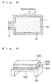
- FIG. 12 is a perspective view showing an example of multi-nozzle head in the first embodiment.
- FIG. 14 is a sectional view of the nozzle head in the third embodiment.
- FIG. 15 is a sectional view of a nozzle head in a fourth embodiment of the invention.
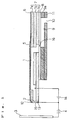
- the pressure chamber 1 is composed of a pressure chamber structure 7 in a three-layer structure made of three layers of photosensitive glass 7a, 7b, 7c, a nickel-made diaphragm 6 formed on the photosensitive glass 7a, and a stainless steel feed side nozzle plate 8 having the tiny hole 16 for passing the ink into the pressure chamber 1.
- the meniscus formed by voltage application of the counter electrode 3 can be held as it is on the way of the nozzle 2, so that ink drooping can be prevented.
- the degree of concentration of electric field on the ink that is, the ink injecting speed and the ink holding force at the nozzle 2 can be controlled, so that optimum conditions can be selected.
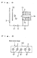
- FIG. 3 shows a state in which voltage is not applied to the counter electrode 3 in this embodiment (the switch 31 is off), and only a voltage is applied between the ink and control electrode 13.
- the ink is not swollen by the counter electrode 3, and the end of the ink is held at an intermediate position of the nozzle 2 by the applied voltage, so that the ink does not droop from the leading end of the nozzle.
- the control electrode 13 and the ink in the nozzle 2 are isolated, and therefore the electric field is not concentrated too much on the ink, and the electrostatic attraction by the counter electrode 3 is not too small, and drooping of the ink from the nozzle 2 can be prevented, and the crosstalk between nozzles can be suppressed.
- concentration of electric field between the counter electrode 3 and ink can be alleviated, crosstalk effects are smaller, and therefore, as shown in FIG. 6, for example, by composing the control electrode commonly by an electrode 60, arranging a plurality of nozzles 2 in a row, and surrounding the electrode 60 and the nozzles 2 by an insulator 61, multiple nozzles may be easily formed.
- drooping of the ink is prevented by holding the leading end of the ink at the nozzle 2 at its position by using the control electrode 13, and it is more effective to prevent drooping of ink by drawing back the ink to the pressure chamber side by using the following method.
- form the leading end portion of the nozzle 2 to a specified distance of inside, or further the leading end of the nozzle 2 may be covered with a water repellent film 70 having a water repellent property made of fluorine film.
- the ink is drawn back to the pressure chamber side as being repelled by the water repellent film 70, and drooping preventive effect is obtained.
- the voltage applied to the control electrode 13 is reverse in polarity to the voltage applied to the counter electrode 3, but, not limited to this, voltages of same polarity may be applied.
- FIG. 13 is a plan view of a nozzle head in a third embodiment of the invention.
- the difference in applied pressure by the control of the individual piezo elements 1302 is large between discharge and stop, and it is free from effects if bias fluctuations of the common piezo element 1301 are significant.
- a uniform meniscus may be easily formed, the required piezoelectric power of the individual piezo elements 1302 may be reduced, and large fluctuations can be ignored, so that a higher density is realized.
- maximum pressure is applied by both common piezo element 1301 and individual piezo elements 1302, powerful discharge is possible for head cleaning or servicing.
Landscapes
- Particle Formation And Scattering Control In Inkjet Printers (AREA)
Priority Applications (1)
| Application Number | Priority Date | Filing Date | Title |
|---|---|---|---|
| EP01130705A EP1199173B1 (de) | 1996-10-29 | 1997-10-28 | Tintenstrahlaufzeichnungsgerät und Verfahren zu seiner Herstellung |
Applications Claiming Priority (3)
| Application Number | Priority Date | Filing Date | Title |
|---|---|---|---|
| JP286479/96 | 1996-10-29 | ||
| JP28647996 | 1996-10-29 | ||
| JP28647996 | 1996-10-29 |
Related Child Applications (1)
| Application Number | Title | Priority Date | Filing Date |
|---|---|---|---|
| EP01130705A Division EP1199173B1 (de) | 1996-10-29 | 1997-10-28 | Tintenstrahlaufzeichnungsgerät und Verfahren zu seiner Herstellung |
Publications (2)
| Publication Number | Publication Date |
|---|---|
| EP0839653A2 true EP0839653A2 (de) | 1998-05-06 |
| EP0839653A3 EP0839653A3 (de) | 1999-06-30 |
Family
ID=17704933
Family Applications (2)
| Application Number | Title | Priority Date | Filing Date |
|---|---|---|---|
| EP97118744A Withdrawn EP0839653A3 (de) | 1996-10-29 | 1997-10-28 | Tintenstrahlaufzeichnungsgerät und Verfahren zu seiner Herstellung |
| EP01130705A Expired - Lifetime EP1199173B1 (de) | 1996-10-29 | 1997-10-28 | Tintenstrahlaufzeichnungsgerät und Verfahren zu seiner Herstellung |
Family Applications After (1)
| Application Number | Title | Priority Date | Filing Date |
|---|---|---|---|
| EP01130705A Expired - Lifetime EP1199173B1 (de) | 1996-10-29 | 1997-10-28 | Tintenstrahlaufzeichnungsgerät und Verfahren zu seiner Herstellung |
Country Status (4)
| Country | Link |
|---|---|
| US (1) | US6341851B1 (de) |
| EP (2) | EP0839653A3 (de) |
| KR (1) | KR100471793B1 (de) |
| DE (1) | DE69739387D1 (de) |
Cited By (3)
| Publication number | Priority date | Publication date | Assignee | Title |
|---|---|---|---|---|
| EP0976560A3 (de) * | 1998-07-29 | 2000-05-10 | Seiko Epson Corporation | Tintenstrahlaufzeichnungskopf und diesen Kopf tragende Tintenstrahlaufzeichnungsvorrichtung |
| EP0963846A3 (de) * | 1998-06-08 | 2000-05-10 | Seiko Epson Corporation | Tintenstrahlaufzeichnungskopf und Tintenstrahlaufzeichnungsvorrichtung |
| US8632166B2 (en) | 2001-06-15 | 2014-01-21 | Semiconductor Energy Laboratory Co., Ltd. | Printing device and method of manufacturing a light emitting device |
Families Citing this family (29)
| Publication number | Priority date | Publication date | Assignee | Title |
|---|---|---|---|---|
| US6392257B1 (en) * | 2000-02-10 | 2002-05-21 | Motorola Inc. | Semiconductor structure, semiconductor device, communicating device, integrated circuit, and process for fabricating the same |
| KR20030011083A (ko) | 2000-05-31 | 2003-02-06 | 모토로라 인코포레이티드 | 반도체 디바이스 및 이를 제조하기 위한 방법 |
| AU2001277001A1 (en) * | 2000-07-24 | 2002-02-05 | Motorola, Inc. | Heterojunction tunneling diodes and process for fabricating same |
| US20020096683A1 (en) * | 2001-01-19 | 2002-07-25 | Motorola, Inc. | Structure and method for fabricating GaN devices utilizing the formation of a compliant substrate |
| WO2002082551A1 (en) | 2001-04-02 | 2002-10-17 | Motorola, Inc. | A semiconductor structure exhibiting reduced leakage current |
| US20020158245A1 (en) * | 2001-04-26 | 2002-10-31 | Motorola, Inc. | Structure and method for fabricating semiconductor structures and devices utilizing binary metal oxide layers |
| US6992321B2 (en) * | 2001-07-13 | 2006-01-31 | Motorola, Inc. | Structure and method for fabricating semiconductor structures and devices utilizing piezoelectric materials |
| US7019332B2 (en) * | 2001-07-20 | 2006-03-28 | Freescale Semiconductor, Inc. | Fabrication of a wavelength locker within a semiconductor structure |
| US6855992B2 (en) * | 2001-07-24 | 2005-02-15 | Motorola Inc. | Structure and method for fabricating configurable transistor devices utilizing the formation of a compliant substrate for materials used to form the same |
| US20030034491A1 (en) | 2001-08-14 | 2003-02-20 | Motorola, Inc. | Structure and method for fabricating semiconductor structures and devices for detecting an object |
| US20030071327A1 (en) | 2001-10-17 | 2003-04-17 | Motorola, Inc. | Method and apparatus utilizing monocrystalline insulator |
| US6916717B2 (en) * | 2002-05-03 | 2005-07-12 | Motorola, Inc. | Method for growing a monocrystalline oxide layer and for fabricating a semiconductor device on a monocrystalline substrate |
| US20040012037A1 (en) * | 2002-07-18 | 2004-01-22 | Motorola, Inc. | Hetero-integration of semiconductor materials on silicon |
| US20040069991A1 (en) * | 2002-10-10 | 2004-04-15 | Motorola, Inc. | Perovskite cuprate electronic device structure and process |
| US20040079285A1 (en) * | 2002-10-24 | 2004-04-29 | Motorola, Inc. | Automation of oxide material growth in molecular beam epitaxy systems |
| US7169619B2 (en) | 2002-11-19 | 2007-01-30 | Freescale Semiconductor, Inc. | Method for fabricating semiconductor structures on vicinal substrates using a low temperature, low pressure, alkaline earth metal-rich process |
| US6885065B2 (en) * | 2002-11-20 | 2005-04-26 | Freescale Semiconductor, Inc. | Ferromagnetic semiconductor structure and method for forming the same |
| US6963090B2 (en) * | 2003-01-09 | 2005-11-08 | Freescale Semiconductor, Inc. | Enhancement mode metal-oxide-semiconductor field effect transistor |
| US7020374B2 (en) * | 2003-02-03 | 2006-03-28 | Freescale Semiconductor, Inc. | Optical waveguide structure and method for fabricating the same |
| US6965128B2 (en) | 2003-02-03 | 2005-11-15 | Freescale Semiconductor, Inc. | Structure and method for fabricating semiconductor microresonator devices |
| US20040164315A1 (en) * | 2003-02-25 | 2004-08-26 | Motorola, Inc. | Structure and device including a tunneling piezoelectric switch and method of forming same |
| US7497962B2 (en) * | 2004-08-06 | 2009-03-03 | Canon Kabushiki Kaisha | Method of manufacturing liquid discharge head and method of manufacturing substrate for liquid discharge head |
| JPWO2006067966A1 (ja) * | 2004-12-20 | 2008-06-12 | コニカミノルタホールディングス株式会社 | 液体吐出ヘッド、液体吐出装置および液体吐出方法 |
| JP4998266B2 (ja) * | 2005-05-11 | 2012-08-15 | コニカミノルタホールディングス株式会社 | 液体吐出装置 |
| JP4458052B2 (ja) * | 2006-03-13 | 2010-04-28 | セイコーエプソン株式会社 | インクジェットヘッドの製造方法 |
| JP2007237718A (ja) * | 2006-03-13 | 2007-09-20 | Seiko Epson Corp | インクジェットヘッドの製造方法 |
| US8006356B2 (en) | 2006-12-07 | 2011-08-30 | Xerox Corporation | Method of forming an array of drop generators |
| WO2014185559A1 (ko) * | 2013-05-13 | 2014-11-20 | 알피니언메디칼시스템 주식회사 | 트랜스듀서 제조방법 및 그 방법에 의해 제조된 트랜스듀서 |
| EP3969285B1 (de) | 2019-07-17 | 2024-04-24 | Scrona AG | Elektrohydrodynamischer druckkopf mit strukturierter zuführschicht |
Family Cites Families (37)
| Publication number | Priority date | Publication date | Assignee | Title |
|---|---|---|---|---|
| JPS585271A (ja) * | 1981-07-02 | 1983-01-12 | Seiko Epson Corp | インクジエツト印刷装置 |
| JPS6046257A (ja) * | 1983-08-24 | 1985-03-13 | Nec Corp | インクジェット記録装置 |
| JPS61106259A (ja) | 1984-10-31 | 1986-05-24 | Hitachi Ltd | インク滴噴出装置 |
| JPS62189168A (ja) * | 1986-02-14 | 1987-08-18 | Nec Corp | ドロツプオンデマンドインクジエツトヘツドの駆動方法 |
| JPS62240559A (ja) * | 1986-04-14 | 1987-10-21 | Toshiba Corp | インクジエツト記録装置 |
| JPS6391258A (ja) * | 1986-10-03 | 1988-04-21 | Shuzo Hattori | インクジエツトヘツド |
| US4879568A (en) | 1987-01-10 | 1989-11-07 | Am International, Inc. | Droplet deposition apparatus |
| JPH03193455A (ja) * | 1989-12-25 | 1991-08-23 | Seiko Epson Corp | インクジェットヘッド |
| JP2913806B2 (ja) * | 1990-09-14 | 1999-06-28 | ブラザー工業株式会社 | 圧電式インクジェットプリンタヘッド |
| US5500988A (en) * | 1990-11-20 | 1996-03-26 | Spectra, Inc. | Method of making a perovskite thin-film ink jet transducer |
| JPH04263951A (ja) * | 1991-02-19 | 1992-09-18 | Seiko Epson Corp | インクジェットヘッド |
| JPH04284253A (ja) * | 1991-03-13 | 1992-10-08 | Brother Ind Ltd | インクジェットプリンタおよびヘッド |
| JPH04329145A (ja) | 1991-04-30 | 1992-11-17 | Fujitsu Ltd | マルチノズルインクジェットヘッド |
| JPH04338548A (ja) * | 1991-05-16 | 1992-11-25 | Tokyo Electric Co Ltd | インクジェットプリンタ |
| US5477249A (en) * | 1991-10-17 | 1995-12-19 | Minolta Camera Kabushiki Kaisha | Apparatus and method for forming images by jetting recording liquid onto an image carrier by applying both vibrational energy and electrostatic energy |
| JPH05124187A (ja) * | 1991-10-31 | 1993-05-21 | Canon Inc | インクジエツト式記録装置および該装置におけるインク液滴制御方法ならびにインクミスト吸着方法 |
| JP3008609B2 (ja) * | 1991-11-13 | 2000-02-14 | 松下電器産業株式会社 | インク吐出装置 |
| JPH05305710A (ja) * | 1992-02-24 | 1993-11-19 | Rohm Co Ltd | インクジェットプリントヘッド及びそれを備える電子機器 |
| JPH05261920A (ja) | 1992-03-18 | 1993-10-12 | Fujitsu Ltd | インクジェットプリントヘッド及びその製造方法 |
| US5221934A (en) * | 1992-04-01 | 1993-06-22 | Eastman Kodak Company | Electrochemical resistive ink jet head |
| JP3379106B2 (ja) | 1992-04-23 | 2003-02-17 | セイコーエプソン株式会社 | 液体噴射ヘッド |
| JP3317308B2 (ja) * | 1992-08-26 | 2002-08-26 | セイコーエプソン株式会社 | 積層型インクジェット記録ヘッド、及びその製造方法 |
| US5271957A (en) * | 1992-06-18 | 1993-12-21 | Eastman Kodak Company | Chemical vapor deposition of niobium and tantalum oxide films |
| JP3106044B2 (ja) | 1992-12-04 | 2000-11-06 | 日本碍子株式会社 | アクチュエータ及びそれを用いたインクジェットプリントヘッド |
| JPH06218917A (ja) * | 1993-01-22 | 1994-08-09 | Sharp Corp | インクジェットヘッド |
| US5736993A (en) * | 1993-07-30 | 1998-04-07 | Tektronix, Inc. | Enhanced performance drop-on-demand ink jet head apparatus and method |
| KR0147245B1 (ko) * | 1993-12-01 | 1998-09-15 | 모리시타 요이찌 | 강유전체박막 및 그 제조방법 |
| US5825121A (en) * | 1994-07-08 | 1998-10-20 | Seiko Epson Corporation | Thin film piezoelectric device and ink jet recording head comprising the same |
| JPH08118662A (ja) * | 1994-10-26 | 1996-05-14 | Mita Ind Co Ltd | インクジェットプリンタ用印字ヘッド及びその製造方法 |
| JPH08132621A (ja) | 1994-11-08 | 1996-05-28 | Matsushita Electric Ind Co Ltd | 液滴吐出装置 |
| EP0736915A1 (de) * | 1995-04-03 | 1996-10-09 | Seiko Epson Corporation | Piezoelektrische Dünnschicht, Verfahren zum Herstellen und Tintenstrahldruckkopf mit Verwendung dieser Dünnschicht |
| JP2865621B2 (ja) * | 1995-06-12 | 1999-03-08 | オセ−ネーデルランド・ビー・ブイ | インクジェットシステム |
| US5923346A (en) * | 1995-10-23 | 1999-07-13 | Imaging Technology International | Shadow pulse compensation of an ink jet printer |
| JP2842343B2 (ja) * | 1995-10-26 | 1999-01-06 | 日本電気株式会社 | 静電式インクジェット記録装置 |
| JP2783220B2 (ja) * | 1995-10-30 | 1998-08-06 | 日本電気株式会社 | インクジェット式記録ヘッド |
| DE69607814T2 (de) * | 1995-12-14 | 2001-01-11 | Nec Corp., Tokio/Tokyo | Elektrostatische Tintenstrahlaufzeichnungsvorrichtung, welche die Tinte ausstösst mittels elektrischen Feldern |
| JPH09221393A (ja) * | 1996-02-13 | 1997-08-26 | Tdk Corp | 鉛含有ペロブスカイト型強誘電体単結晶膜及びその製造方法 |
-
1997
- 1997-10-28 EP EP97118744A patent/EP0839653A3/de not_active Withdrawn
- 1997-10-28 EP EP01130705A patent/EP1199173B1/de not_active Expired - Lifetime
- 1997-10-28 DE DE69739387T patent/DE69739387D1/de not_active Expired - Lifetime
- 1997-10-29 KR KR1019970055820A patent/KR100471793B1/ko not_active Expired - Fee Related
-
2000
- 2000-01-19 US US09/487,221 patent/US6341851B1/en not_active Expired - Fee Related
Cited By (5)
| Publication number | Priority date | Publication date | Assignee | Title |
|---|---|---|---|---|
| EP0963846A3 (de) * | 1998-06-08 | 2000-05-10 | Seiko Epson Corporation | Tintenstrahlaufzeichnungskopf und Tintenstrahlaufzeichnungsvorrichtung |
| US6336717B1 (en) | 1998-06-08 | 2002-01-08 | Seiko Epson Corporation | Ink jet recording head and ink jet recording apparatus |
| EP0976560A3 (de) * | 1998-07-29 | 2000-05-10 | Seiko Epson Corporation | Tintenstrahlaufzeichnungskopf und diesen Kopf tragende Tintenstrahlaufzeichnungsvorrichtung |
| US6502928B1 (en) | 1998-07-29 | 2003-01-07 | Seiko Epson Corporation | Ink jet recording head and ink jet recording apparatus comprising the same |
| US8632166B2 (en) | 2001-06-15 | 2014-01-21 | Semiconductor Energy Laboratory Co., Ltd. | Printing device and method of manufacturing a light emitting device |
Also Published As
| Publication number | Publication date |
|---|---|
| EP1199173A2 (de) | 2002-04-24 |
| KR19980033257A (ko) | 1998-07-25 |
| US6341851B1 (en) | 2002-01-29 |
| EP0839653A3 (de) | 1999-06-30 |
| KR100471793B1 (ko) | 2005-07-04 |
| DE69739387D1 (de) | 2009-06-10 |
| EP1199173B1 (de) | 2009-04-29 |
| EP1199173A3 (de) | 2003-03-05 |
Similar Documents
| Publication | Publication Date | Title |
|---|---|---|
| US6341851B1 (en) | Ink jet recording apparatus including a pressure chamber and pressure applying means | |
| US6394363B1 (en) | Liquid projection apparatus | |
| US4584590A (en) | Shear mode transducer for drop-on-demand liquid ejector | |
| JP4829165B2 (ja) | 圧電素子製造方法及び液体吐出ヘッド製造方法 | |
| JPH0661936B2 (ja) | パルス滴付着装置およびパルス滴付着装置の製造方法 | |
| JPH05301342A (ja) | インクジェットプリンタ用ヘッド | |
| JP2715001B2 (ja) | 2つのu字型チャンネル駆動装置を持つ高密度インクジェットプリンタヘッド | |
| US4188635A (en) | Ink jet printing head | |
| KR960003359B1 (ko) | 잉크제트 시스템용 압전 변환기 및 잉크제트 시스템 | |
| EP0658142B1 (de) | Tintenstrahldruckkopf | |
| JP2003008091A (ja) | ダイアフラム型圧電アクチュエータ及びインクジェットヘッド | |
| JP2867740B2 (ja) | 液滴噴射装置 | |
| JP3384958B2 (ja) | インクジェット記録装置とその製造方法 | |
| US6505920B1 (en) | Synchronously stimulated continuous ink jet head | |
| JP3149663B2 (ja) | インク噴射装置 | |
| JP3064455B2 (ja) | インクジェットヘッド | |
| JP3213126B2 (ja) | インクジェット記録装置の印字ヘッド | |
| US20240278557A1 (en) | Liquid droplet discharging apparatus | |
| JPH10278267A (ja) | インクジェット記録装置 | |
| JPH04294146A (ja) | インクジェットヘッド | |
| JPH02297445A (ja) | インクジェットプリンタのインク吐出装置 | |
| JP2729008B2 (ja) | インクジェット記録ヘッド装置 | |
| JPH04263951A (ja) | インクジェットヘッド | |
| JP2006069112A (ja) | インクジェット記録ヘッド及びインクジェット記録装置 | |
| JPH05338155A (ja) | インクジェットヘッド |
Legal Events
| Date | Code | Title | Description |
|---|---|---|---|
| PUAI | Public reference made under article 153(3) epc to a published international application that has entered the european phase |
Free format text: ORIGINAL CODE: 0009012 |
|
| AK | Designated contracting states |
Kind code of ref document: A2 Designated state(s): DE FR GB IT NL |
|
| AX | Request for extension of the european patent |
Free format text: AL;LT;LV;RO;SI |
|
| PUAL | Search report despatched |
Free format text: ORIGINAL CODE: 0009013 |
|
| 17P | Request for examination filed |
Effective date: 19990427 |
|
| AK | Designated contracting states |
Kind code of ref document: A3 Designated state(s): AT BE CH DE DK ES FI FR GB GR IE IT LI LU MC NL PT SE |
|
| AX | Request for extension of the european patent |
Free format text: AL;LT;LV;RO;SI |
|
| AKX | Designation fees paid |
Free format text: DE FR GB IT NL |
|
| 17Q | First examination report despatched |
Effective date: 20000927 |
|
| GRAH | Despatch of communication of intention to grant a patent |
Free format text: ORIGINAL CODE: EPIDOS IGRA |
|
| STAA | Information on the status of an ep patent application or granted ep patent |
Free format text: STATUS: THE APPLICATION IS DEEMED TO BE WITHDRAWN |
|
| 18D | Application deemed to be withdrawn |
Effective date: 20030222 |