EP0845792B1 - Verfahren zur Herstellung eines drahtgewickelten elektronischen Bauelements - Google Patents
Verfahren zur Herstellung eines drahtgewickelten elektronischen Bauelements Download PDFInfo
- Publication number
- EP0845792B1 EP0845792B1 EP97309130A EP97309130A EP0845792B1 EP 0845792 B1 EP0845792 B1 EP 0845792B1 EP 97309130 A EP97309130 A EP 97309130A EP 97309130 A EP97309130 A EP 97309130A EP 0845792 B1 EP0845792 B1 EP 0845792B1
- Authority
- EP
- European Patent Office
- Prior art keywords
- coil
- block
- flanges
- bobbin
- coating
- Prior art date
- Legal status (The legal status is an assumption and is not a legal conclusion. Google has not performed a legal analysis and makes no representation as to the accuracy of the status listed.)
- Expired - Lifetime
Links
Images












Classifications
-
- H—ELECTRICITY
- H01—ELECTRIC ELEMENTS
- H01F—MAGNETS; INDUCTANCES; TRANSFORMERS; SELECTION OF MATERIALS FOR THEIR MAGNETIC PROPERTIES
- H01F41/00—Apparatus or processes specially adapted for manufacturing or assembling magnets, inductances or transformers; Apparatus or processes specially adapted for manufacturing materials characterised by their magnetic properties
- H01F41/02—Apparatus or processes specially adapted for manufacturing or assembling magnets, inductances or transformers; Apparatus or processes specially adapted for manufacturing materials characterised by their magnetic properties for manufacturing cores, coils, or magnets
- H01F41/04—Apparatus or processes specially adapted for manufacturing or assembling magnets, inductances or transformers; Apparatus or processes specially adapted for manufacturing materials characterised by their magnetic properties for manufacturing cores, coils, or magnets for manufacturing coils
- H01F41/12—Insulating of windings
- H01F41/127—Encapsulating or impregnating
-
- H—ELECTRICITY
- H01—ELECTRIC ELEMENTS
- H01F—MAGNETS; INDUCTANCES; TRANSFORMERS; SELECTION OF MATERIALS FOR THEIR MAGNETIC PROPERTIES
- H01F17/00—Fixed inductances of the signal type
- H01F17/04—Fixed inductances of the signal type with magnetic core
- H01F17/045—Fixed inductances of the signal type with magnetic core with core of cylindric geometry and coil wound along its longitudinal axis, i.e. rod or drum core
-
- H—ELECTRICITY
- H01—ELECTRIC ELEMENTS
- H01F—MAGNETS; INDUCTANCES; TRANSFORMERS; SELECTION OF MATERIALS FOR THEIR MAGNETIC PROPERTIES
- H01F27/00—Details of transformers or inductances, in general
- H01F27/28—Coils; Windings; Conductive connections
- H01F27/29—Terminals; Tapping arrangements for signal inductances
- H01F27/292—Surface mounted devices
-
- H—ELECTRICITY
- H01—ELECTRIC ELEMENTS
- H01F—MAGNETS; INDUCTANCES; TRANSFORMERS; SELECTION OF MATERIALS FOR THEIR MAGNETIC PROPERTIES
- H01F41/00—Apparatus or processes specially adapted for manufacturing or assembling magnets, inductances or transformers; Apparatus or processes specially adapted for manufacturing materials characterised by their magnetic properties
- H01F41/02—Apparatus or processes specially adapted for manufacturing or assembling magnets, inductances or transformers; Apparatus or processes specially adapted for manufacturing materials characterised by their magnetic properties for manufacturing cores, coils, or magnets
- H01F41/04—Apparatus or processes specially adapted for manufacturing or assembling magnets, inductances or transformers; Apparatus or processes specially adapted for manufacturing materials characterised by their magnetic properties for manufacturing cores, coils, or magnets for manufacturing coils
- H01F41/10—Connecting leads to windings
-
- Y—GENERAL TAGGING OF NEW TECHNOLOGICAL DEVELOPMENTS; GENERAL TAGGING OF CROSS-SECTIONAL TECHNOLOGIES SPANNING OVER SEVERAL SECTIONS OF THE IPC; TECHNICAL SUBJECTS COVERED BY FORMER USPC CROSS-REFERENCE ART COLLECTIONS [XRACs] AND DIGESTS
- Y10—TECHNICAL SUBJECTS COVERED BY FORMER USPC
- Y10T—TECHNICAL SUBJECTS COVERED BY FORMER US CLASSIFICATION
- Y10T29/00—Metal working
- Y10T29/49—Method of mechanical manufacture
- Y10T29/49002—Electrical device making
- Y10T29/4902—Electromagnet, transformer or inductor
-
- Y—GENERAL TAGGING OF NEW TECHNOLOGICAL DEVELOPMENTS; GENERAL TAGGING OF CROSS-SECTIONAL TECHNOLOGIES SPANNING OVER SEVERAL SECTIONS OF THE IPC; TECHNICAL SUBJECTS COVERED BY FORMER USPC CROSS-REFERENCE ART COLLECTIONS [XRACs] AND DIGESTS
- Y10—TECHNICAL SUBJECTS COVERED BY FORMER USPC
- Y10T—TECHNICAL SUBJECTS COVERED BY FORMER US CLASSIFICATION
- Y10T29/00—Metal working
- Y10T29/49—Method of mechanical manufacture
- Y10T29/49002—Electrical device making
- Y10T29/4902—Electromagnet, transformer or inductor
- Y10T29/49071—Electromagnet, transformer or inductor by winding or coiling
-
- Y—GENERAL TAGGING OF NEW TECHNOLOGICAL DEVELOPMENTS; GENERAL TAGGING OF CROSS-SECTIONAL TECHNOLOGIES SPANNING OVER SEVERAL SECTIONS OF THE IPC; TECHNICAL SUBJECTS COVERED BY FORMER USPC CROSS-REFERENCE ART COLLECTIONS [XRACs] AND DIGESTS
- Y10—TECHNICAL SUBJECTS COVERED BY FORMER USPC
- Y10T—TECHNICAL SUBJECTS COVERED BY FORMER US CLASSIFICATION
- Y10T29/00—Metal working
- Y10T29/49—Method of mechanical manufacture
- Y10T29/49002—Electrical device making
- Y10T29/4902—Electromagnet, transformer or inductor
- Y10T29/49075—Electromagnet, transformer or inductor including permanent magnet or core
- Y10T29/49076—From comminuted material
Definitions
- the present invention relates to an inductor, transformer, choke coil or similar wire wound electronic component.
- Japanese Utility Model Laid-Open Publication No. 51-115547 teaches a fixed inductance device having a bobbin made up of a core and flanges, conductive layers formed on the circumferential surfaces of the flanges, and a coil wound round the core. A conductor protruding from opposite stripped ends of the coil is connected to the conductive layers and to conductive portions provided on a printed circuit board.
- Japanese Utility Model Laid-Open Publication No. 56-110612 discloses an inductance device having flanges formed with grooves, and a coil whose conductor is received in the grooves at both ends thereof.
- Japanese Patent Laid-Open Publication No. 57-73916 proposes a miniature inductor including a core, flanges formed at both ends of the core, conductive layers respectively formed on the flanges, and a coil wound round the center of the core.
- electrodes are formed after the assembly has been sealed with a resin.
- Japanese Utility Model Laid-Open Publication No. 61-144616 discloses a chip coil in which a conductor protruding from opposite stripped ends of a coil is drawn out via grooves formed in rectangular flanges, and electrodes are also formed on the sides of the flanges.
- a wire wound electronic component has a coil wound round a core and has a conductor protruding from the coil bonded to the electrodes of flanges.
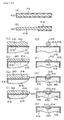
- Such a wire wound electronic component may be produced by a method shown in FIG. 27.
- FIG. 27 A
- a bobbin having a core 900 and flanges 902 formed at both ends of the bobbin 900 is prepared.
- electrodes 904 are respectively formed on the sides and end faces of the flanges 902 by dipping or similar technology.
- a coil 906 is wound round the core 900 and has its outgoing conductor 908 connected to the electrodes 904 by, e.g., heat pressure welding.
- a resin or a paint is applied to the core portion, which was wound the coil 906, in order to form a coating or armor 910.
- a plating 912 of, e.g., Ni is formed on each electrode 904.
- the assembly is entirely trimmed into a column having a rectangular cross-section.
- a method of producing a wire wound electronic component comprising the steps of: providing a bobbin comprising a core, one or more flanges wherein at least one flange is at one end of said core, and external electrodes on said one or more flanges; winding a sheathed conductor around said core to form a coil and electrically connecting the coil to said external electrodes, and forming a coating having a flat surface on said coil, characterised in that the step of forming the coating comprises pressing the coating towards the coil so that the coating penetrates gaps between the turns of the coil.
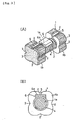
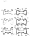
- the bobbin 1 has a core 1a having a circular cross-section and rectangular flanges 1b formed at both ends of the core 1a.
- the flanges 1b are sized 0.8 mm square by way of example and formed of ferrite or similar material.
- a groove 2 having a generally V-shaped cross-section and, e.g., 0.06 mm depth is formed in each side of each flange 1b.
- a conductive film or external electrode 3 is formed on the four sides and end face of each flange 1b.
- the conductive film 3 is made up of an underlying layer mainly consisting of silver, silver-platinum alloy or copper and an overlying layer of nickel or lead-tin alloy.
- a coil i.e., a sheathed wire 4 is wound round the core 1a of the bobbin 1 and formed of polyurethane, polyamide-imide or similar insulating material.
- the coil 4 has a diameter of, e.g., 20 ⁇ m to 120 ⁇ m.
- Opposite ends 5 of the coil 4, i.e., opposite ends of a conductor protruding from the stripped ends of the coil 4 are respectively received in the V-shaped grooves 2 of the flanges 1b and bonded to the conductive films 3 by welding, heat pressure welding or ultrasonic oscillation welding.
- the coil 4 can be wound round the core 1a in close contact with the surface of the core 1a. This reduces the scattering of inductance and protects the sheath of the wire from damage, compared to a bobbin having a rectangular core.
- a coating or armor portion 6 is formed on the entire circumference of the coil 4 and formed of an epoxy resin (with or without a filler) or similar insulator. To form the coating 6, use may be made of potting.
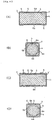
- the surface of the coating 6 is flattened such that it is positioned inward of the peripheries of the flanges 1b while its portions corresponding to the corners of the flanges 1b protrude to the outside of the incircles of the flanges 1b.
- the coating 6 has a rectangular cross-section complementary to the configuration of each flange 1b and has its surface positioned inward of the flange 1b.
- the magnetic bobbin 1 may be replaced with a bobbin formed of alumina or similar insulator.
- the coating 6 is provided on the entire periphery of the coil 6.
- the coating 6 may be formed only on the intermediate portion of the coil 4 with or without a constant width.
- the chip inductor can be readily transferred to a position above a printed circuit board only if a suction nozzle included in an automatic mounting machine is applied to the surface, labeled 6a, of the coating 6 so as to suck it. Subsequently, the conductive films 3 of the flanges 1b are soldered to a conductive pattern formed on the circuit board. With this configuration, it is not necessary to consider the mounting surface of the chip inductor when the inductor is mounted to the printed circuit board. In addition, because the flanges 1b of the bobbin 1 are rectangular, the chip inductor is prevented from rolling.
- each flange 1b of the bobbin 1 is controllable in order to provide the conductive film 3 with a desired configuration.
- the film 3 may be formed on each side of the flange 1b over only a part of the width of the side.
- the film 3 may extend even to the inner surface of the flange 1b.
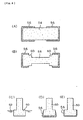
- the grooves 2 formed in the flanges 1b for receiving the ends 5 of the coil 4 are not essential. As shown in FIG. 2, (C) or (D), the ends 5 of the coil 4 may be inclined with respect to the thicknesswise direction of the flanges 2b or may even be bent along the contour of the flanges 1b when they are connected to the conductive films 3. Again, the ends 5 of the coil 4 are bonded to the films 3 in a flat configuration by welding, heat pressure welding or ultrasonic oscillation welding.
- FIG. 3 Another specific configuration of the chip inductor is shown in FIG. 3, (A) and (B).
- the coating 6 is formed only on the part of the coil 4 corresponding to one of four sides of the flanges 1b.
- the surface 6a of the coating 6 is flat and positioned inward of the contour of the flanges 1b.
- this chip inductor is identical with the chip inductor shown in FIG. 1, (A)-(D).
- the coating 6 may be provided on the portion or portions of the coil 4 corresponding to one or two of the other sides of the flanges 1b.
- FIG. 4 Still another specific configuration of the chip inductor is shown in FIG. 4, (A) and (B).
- the inductor has a bobbin 11 formed of a magnetic material or an insulating material and also provided with a generally circular cross-section.
- a coil or sheathed wire 4 is wound round the bobbin 11.
- Conductive caps or external electrodes 7 each having a rectangular configuration are respectively fitted on opposite ends of the bobbin 11 in pressing contact with the ends 5 of the coil 4.
- the coating 6 formed of resin, for example, is formed on the entire circumference of the coil 4.
- the coating 6 has a rectangular cross-section complementary to that of the caps 7.
- the flat surface 6a of the coating 6 is positioned inward of the caps 7, as in the example shown in FIG. 1, (A)-(D).
- FIG. 4, (C) and (D) A modification of the example shown in FIG. 4, (A) and (B), is shown in FIG. 4, (C) and (D).
- the modification is identical with the example of FIG. 4, (A) and (B).
- the coating 6 may be formed only in the intermediate portion of the coil 4, as shown in FIG. 1, (C) and (D), or may be provided only in the portion of the coil 4 corresponding to at least one of four sides of each cap 7, as shown in FIG. 3, (A) and (B).
- the surface of the coating 6 should only be flat enough to be sucked by the suction nozzle of an automatic mounting machine. Specifically, the flatness may only be of such a degree that the coating 6 has a cross-section not concentric with the core 1a and reduces the irregularities ascribable to the turns of the coil 4 in the axial direction of the core 1a. While the coating 6 has been shown and described as being positioned inward of the peripheries of the flanges 1b or those of the caps 7, the former may be made flush with the latter or may even be positioned outside of the peripheries of the latter for mounting reasons.
- the flanges 1b may each be provided with a polygonal configuration with or without rounded corners, if desired.
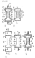
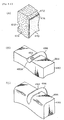
- FIG. 5 shows another method of producing a bobbin.
- FIG. 5 is a section along line #1-#1 shown in (A).
- a block 10 forming a bobbin has a rectangular cross-section.
- a recess 12 is formed in each of opposite end faces of the block 10 for a centering purpose. While the block 10 is rotated by being centered at its recesses 12, as indicated by arrows F1 shown in FIG. 5, (B), the intermediate portion of the block 10 is shaved.
- FIG. 5, (C) a bobbin 18 having a cylindrical core 14 and rectangular flanges 16 formed at both ends of the core 14 is produced. If necessary, the corners of the bobbin 18 may be rounded, as shown in FIG. 5, (D).
- portions 20 where the core 14 and flanges 16 adjoin each other may be provided with a curvature in order to enhance the rigid connection of the core 14 and flanges 16.
- the end portions of the flanges 16 formed with the recesses 12 may be left as they are, or may be cut away at a position indicated by arrows F2 in FIG. 5, (C), and then rounded, as shown in FIG. 5, (D).
- FIG. 6, (A) shows another specific block 22 for forming a bobbin.
- the block 22 has projections or tapered ends 24 and is shaved by being centered at the tapered ends 24.
- FIG. 6, (B) shows the resulting bobbin having a core 24 and flanges 28.
- the projections 24 may be cut away, if necessary.
- FIG. 6, (D) shows another specific block 30 for forming a bobbin.
- leads 32 are bonded to opposite ends of the block 30. The block 30 is rotated with the leads 32 serving as the center.
- the block 30 is formed with a core 34 and flanges 34, as shown in FIG. 6, (E).
- the leads 32 may be left as they are or may be cut away like the recessed ends 12 or the projecting ends 24.
- FIG. 7, (A) shows another specific block 40 for forming a bobbin.
- the block 40 has a rectangular cross-section and is formed with grooves 42 in its four sides.
- the block 40 is machined to form a core and flanges in the previously stated manner while being chucked at its grooves 42, as indicated by arrows F3.
- FIG. 7, (C) shows another specific block 44 formed with grooves 46 having a V-shaped cross-section in its sides and ends. The grooves 46 intersect each other at the end faces of the block 44.
- the block 44 is formed with a core and flanges while being chucked at its points 48 where the grooves 46 intersect each other.
- FIG. 7, (D) shows the resulting bobbin.
- the block shown in any one of FIGS. 5-7 can be accurately centered and therefore accurately machined. This allows electrodes to be efficiently formed and allows a coil to be efficiently wound later.
- a flange is to be formed at only one end of the bobbin, one of the recesses or projections will be formed on the flange while the other recess or projection will be formed on the core.
- FIG. 8 shows a method of forming electrodes on flanges.
- a flange 50 is formed with an electrode 56 by, e.g., being dipped in a paste 52 which includes silver liquid or similar liquid as the main components.
- a paste 52 which includes silver liquid or similar liquid as the main components.
- electrodes 56 are formed on a block 54 by dipping or similar method beforehand.
- the entire block 54 may be covered with a conductive film, if desired.
- the block 54 is machined to form a core 58 and flanges 60, as in the previous embodiments.
- the electrodes 56 are partly shaved off, as shown in FIG. 8, (B). This not only allows the electrodes 56 to be accurately formed, but also allows L(inductance) and Q(quality factor) to be accurately adjusted.
- the paste 52 when the paste 52 has a low viscosity, the electrode 56 is formed along the surface of the flange 50 in a relatively flat configuration. As shown in FIG. 8, (D), when the paste 52 has a high viscosity, the electrode 56 bulges out and has a desirably great thickness at the corners of the flange 60. Therefore, the paste 52 should preferably have a high viscosity. If desired, a dipping liquid having a low viscosity and a dipping liquid having a high viscosity may be applied one after the other. For example the liquid with a low viscosity and the liquid with a high viscosity may be sequentially applied in this order.
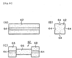
- a block 62 for forming a bobbin is machined before baking.
- the block 62 formed of ceramics and having a rectangular cross-section is prepared before baking.
- grooves 64 are formed in the four sides of the block 62.
- the block 62 easy to machine in such a condition is formed with a core 66 and flanges 68, as shown in FIG. 9, (C).
- the block 62 may be centered by any one of the schemes stated earlier. Subsequently, the block 62 with the core 66 and flanges 68 is baked.
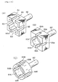
- FIG. 10 shows another example.
- caps 84 each having a lead 82 are fitted on both ends of a bobbin 80.
- the bobbin 80 has a core 86 and flanges 85 formed at both ends of the core 86. Electrodes 81 are respectively formed on the flanges 85. If desired, any one of the previously stated columnar blocks may be substituted for the bobbin 80 and machined to form the core 86 and flanges 85 by being centered at the leads 82.
- FIG. 11, (A) shows a specific configuration of each cap 84.
- the cap 84 has a bore 89A for receiving the flange 85 of the bobbin 80.
- the wall of the bore 89A is formed with slits or windows 83 at positions for connecting leads.
- FIG. 10, (B) shows the bobbin 80 with the caps 84 fitted thereon.
- a coil 90 is wound such that it extends from the leads 82 to the core 86 over the flanges 85.
- a conductor protruding from opposite stripped ends of the coil 90 is bonded to the electrode 81 by solder 91 via the slits 83 of the caps 84.
- a coating or armor of resin 92 is formed on the portion of the coil 90 wound round the core 86.
- the caps 84 are removed from the bobbin 80 by, e.g., being pulled with the soldered portions of the coil 90 being pressed.
- the conductor of the coil 90 is cut off, as shown in FIG. 10, (E).
- the electrodes 81 and soldered portions of the bobbin 80 are plated with, e.g., Ni (not shown).
- FIG. 11, (B) and (C) Other specific configurations of the cap 84 are shown in FIG. 11, (B) and (C).
- a cap 84 has a rectanglar bore 89A and applicable to a block having a rectanglar cross-section.
- a cap 84A has a circular bore 89B, as distinguished from the rectangular bore 89A shown in (A), and slits 83A.
- the cap 84A is usable when the block 80 for forming a bobbin has a circular cross-section.
- a cap 84B also has a circular bore 89C and slits 83B and applicable to a block having a circular cross-section.
- a wire wound electronic component can be produced by use of an existing production line for parts with leads.
- FIG. 12 shows another example which also uses caps.
- the flanges of a bobbin should preferably have flat surfaces from the mounting standpoint and have no directivity from the bulk mounting standpoint.
- a rectangle is one of the shapes of the flanges satisfying the above conditions.
- a cylinder is desirable from the easy machining standpoint.
- rectangular flange caps are bonded to opposite ends of a cylindrical core.
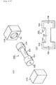
- a cylindrical block 100 is made up of a core 104 and comparatively thick ends portions 104. Recesses 106 are formed in the opposite end faces of the block 100 for the centering purpose.
- Flange caps 108 each has a circular bore 110 corresponding to the shape of the end portion 104. The end portions 104 are respectively press-fitted in or adhered to the bores 110 of the flange caps 108.
- FIG. 12, (B) shows the resulting assembly. In this manner, a bobbin having a cylindrical core and rectangular flanges is produced. Each flange cap 108 may be formed with grooves beforehand, if desired.
- FIG. 13 shows modifications of the above example.
- FIG. 13, (A) shows a cylindrical core member 120 and flange caps 124 each having a bore 122.
- the flange caps 124 are affixed to the end portions of the core member 120 by an adhesive 126.
- the flange caps 124 may each have a rectangular end, as shown in FIG. 13, (B).
- grooves 128 may be formed in the four sides of each flange cap 124.
- FIG. 13, (D) shows a cylindrical core member 130 and flange caps 134 each being formed with a through bore 132.
- the flange caps 134 are also affixed to the core member 130 by an adhesive 136.
- FIG. 13, (E) shows the end of the assembly of FIG. 13, (D).
- each cap may be formed with grooves, as needed.
- Each cap may be formed of ceramics and provided with an electrode on its surface or may be entirely formed of metal. This will allow the entire flanges to serve as heat radiators.
- For the adhesive use may be made of an insulating resin, conductive adhesive, solder or the like.
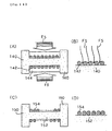
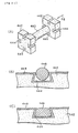
- FIG. 14, (A) shows an embodiment of the present invention, which relates to a coil.
- a bobbin 140 has a coil 142 wound thereround.
- a paint 144 is applied to the coil 142 in the form of a coating.
- the paint 144 is pressed toward the coil 142, as indicated by arrows F5.
- FIG. 14, (B) shows a bobbin 150 including a core 152 whose surface is roughened.
- the rough surface of the core 152 prevents the turns of the coil 154 from being dislocated.
- FIG. 15 shows other examples relating to the positions where the conductor of a coil is connected to electrodes portions(corresponding to flanges and electrodes).
- FIG. 15, (A) shows electrode portions 200 an 202 having grooves 204 and 206, respectively. As shown, the grooves 204 and 206 are deviated from each other with respect to the lengthwise direction of the bobbin.
- a coil 208 has conductor portions 210 and 212 bonded to electrodes in the grooves 204 and 206, respectively. With this configuration, it is possible to reduce the stress ascribable to the shrinkage of a coating resin.
- FIG. 15, (B) shows an electrode portion 220 formed with grooves 222, 224, 226 and 228, and an electrode portion 230 formed with grooves 232, 234, 236 and 238.
- the number of turns of the coil 208 is variable, depending on the grooves to which the stripped portions 210 and 212 of the coil 208 are connected. This allows L and Q to be readily adjusted in order to enhance productivity.
- FIG. 15, (C) shows a bobbin having a rectangular cross-section and including an electrode portion 240 and a flange portion 244. Grooves 242 and 246 are respectively formed in the electrode portion 240 and flange portion 244, but in different planes of the rectangle. This also allows the number of turns of the coil 208 and therefore L and Q to be adjusted with ease. If desired, the configurations shown in FIG. 15, (B) and (C) may be combined in order to adjust L and Q with higher accuracy.
- FIG. 16 shows another comparative example which applies a paint or a resin to a coil in two consecutive steps.
- a paint 314 is applied to a coil 312 in a cylindrical configuration.
- the coil 312 is wound round a bobbin 310(electrodes are not shown).
- a paint 316 is applied over the paint 314 in a rectangular configuration.
- the undercoating 314 has a low viscosity, it will successfully penetrate into the gaps between the turns of the coil 312, surely affixing the coil 312 and insulating its turns. If the overcoating 316 has a high viscosity, it can have its thickness adjusted and trimmed. Three or more paints may be sequentially applied, if desired.
- FIG. 17 shows other examples.
- FIG. 17, (A) shows a core 350 having a coil 352 wound thereround.
- a conductor protruding from opposite stripped ends of the coil 352 are bonded to electrodes 356 formed on flanges 354, but a gap 360 exists between each electrode 356 and a coating or armor 358.
- the gap 360 is apt to bring about various troubles including the breakage of the coil 352.
- a protective coating 362 is provided on the coating 358.
- a conductive resin 364 is applied by dipping or transfer and bonded to the electrode 356, and then a plating 366 is formed on the conductive resin 364.
- the protective coating 362 protects such gaps 360 and thereby obviates the above troubles.
- FIG. 17, (C) shows a structure in which the gaps 360 are protected by a conductive resin 363.
- FIG. 18 shows more examples.
- a wire to be used as a coil is made up of a conductor 410 and a covering 412 covering the conductor 410 and formed of an insulator.
- the covering 412 is removed by some suitable method.
- the surface of the conductor 410 is roughened in order to form irregularities (rough surface) 414. This can be done only if, e.g., the surface of the conductor 410 is mechanically rubbed when the covering 412 is peeled off.
- the conductor 410 with the irregularities 414 is positioned on an electrode 418 formed on a flange 416. In this condition, the conductor 410 is bonded to the electrode 418 by heat pressure welding, ultrasonic welding or similar technology.
- the conductor 410 bites deeply into the electrode 418 due to the irregularities 414. This increases the bonding strength due to a so-called anchor effect.
- FIG. 18, (G)-(K) A modification of the illustrative example is shown in FIG. 18, (G)-(K).
- the flange 416 is formed with a groove 420 having a generally U-shaped section (see (G) and (H)).
- the irregularities 414 of the conductor 410 are entangled with the electrode 418. This also increases the bonding strength between the conductor 410 and electrode 418 (see (I) and (J)).
- the conductor 410 may be fully received in the groove 420 in order to facilitate mounting.
- the groove 420 increases the area over which the conductor 410 and electrode 418 are bonded together. This further increases the bonding strength.
- the conductor 410 is received in the groove 420 while protruding from the electrode 418 little. Consequently, the electrode 418 can be stably bonded to an electrode pattern formed on a circuit board (not shown).
- FIG. 19 shows another example.
- a bobbin 430 has flanges 432 at opposite ends thereof.
- Each flange 432 has its side face and end face covered with an electrode 434.
- FIG. 19, (B) and (C) are fragmentary sections along line #2-#2 of FIG. 19, (A).
- the electrodes 434 are implemented by a silver paste or similar conductive paste containing glass frit as a binder.
- a conductive adhesive (or conductive resin) contains an organic component (e.g. epoxy resin, phenol resin or acryl resin) as a binder.
- each electrode 434 is configured such that the density of glass frit 434A is high in the vicinity of the flange 432 and sequentially decreases toward the its surface, as indicated by a double-headed arrow in FIG. 19, (B). Stated another way, the glass frit 434 is densely arranged in the vicinity of the flange 432 while silver particles 434B are densely arranged in the vicinity of the surface of the electrode 434 so as to form a rough surface.
- a conductor 436 included in a coil (not shown) is bonded to the electrode 434 by heat pressure welding or similar technology.
- the bonding strength of a silver paste increases with an increase in the density of glass frit. Therefore, a core material constituting the flange 432 and the silver paste forming the electrode 434 can be connected together by a great bonding strength due to the high glass frit density.
- the silver particles 434B forming the rough surface ensure rigid bond between the silver paste and the conductor 436 due to the anchor effect, as in the previous example.
- the above example enhances both the close contact of the electrode 434 and flange 432 and the rigid bond between'the electrode 434 and the conductor 436, providing the assembly with high reliability.
- a groove may be formed in the flange 432 in order to further enhance the rigid bond, as in the previous example.
- the electrode 434 may be implemented as a plurality of layers, if desired.
- the electrode 432 may be made up of a silver electrode 431 formed on the flange 432 and an Sn-Pb plating layer 433 formed on the silver electrode 431.
- the conductor 436 is positioned on the plating layer 433 and subjected to fusion bonding (including alloy bonding) using an ultrasonic wave and heat. This is also successful to achieve the advantages of the second embodiment.
- the mechanical bonding shown in FIG. 19 or the fusion bonding shown in FIG. 20, (A) may be replaced with diffusion bonding in which a conductor and an underlying material are bonded by dispersion. Of course, two or more of the above bonding schemes may be combined.
- the position 434P where the end of the electrode 434 is located on the side face of the flange 432 may be adjusted in the direction indicated by a double-headed arrow. This also allows the bonding strength between the electrode 434 and the conductor 436 to be adjusted.
- the specific configuration shown in FIG. 20, (B), includes grooves 438 having a relatively great width. The grooves 438 each allows the conductor 436 to be bonded to the electrode 434 in its oblique position with respect to the lengthwise direction of the bobbin (double-headed arrow F7). The conductor 436 is therefore free from sharp bends and therefore from breakage.
- FIG. 21 shows another example.
- a bobbin has a cylindrical core 440 and rectangular flanges 441 formed at opposite ends of the core 440.
- Each flange 442 is formed with grooves 444 in its four sides; each groove 444 is located at substantially the center of the respective side.
- FIG. 21, (B) is a section as seen in the direction indicated by an arrow F8 in FIG. 21, (A).
- an electrode 448 is formed on the surface of each flange 442.
- a conductor 446 included in a coil is received in the groove 444 and bonded to the electrode 448.
- the grooves 444 each is tapered from the inside toward the outside of the flange 442. Therefore, as shown in FIG. 21, (C), the conductor 446 bonded to the electrode 448 bites into the walls of the groove 444.
- the bonding strength between an electrode and a conductor depends on bonding conditions and is apt to cause the conductor to come off.
- the conductor 446 biting into the walls of the tapered groove 444 maintain the bond despite some scattering in bonding conditions. This prevents the conductor 446 from coming off the electrode.
- FIG. 22 shows another example.
- (A) is a perspective view
- (B) is a section along line #3-#3 of (A)
- (C) is an enlarged view of a conductor bonding portion.
- a bobbin has a cylindrical core 450, a coil 452 wound thereround, and flanges 454 formed at opposite ends of the core 450.
- a through hole 456 extends throughout each flange 454 in the lengthwise direction of the bobbin.
- An electrode 458 is formed on the four sides and end of each flange 454.
- the coil 452 is stripped off at its both ends in order to expose its conductor 460.
- the opposite ends of the conductor 460 are respectively inserted into the through holes 456 of the flanges 454 and bonded to the electrodes 458 by, e.g., a conductive paste, as best shown in FIG. 22, (C).
- the conductor 460 is not positioned on the sides of the flanges 454, but is inserted into the flanges 454. In this condition, a minimum of extraneous force is allowed to act on the conductor 460, so that the bond between the conductor 460 and the electrode 458 is ensured. Further, because the sides of the flanges 454 are simply flat, the electrodes 458 can be desirably bonded to a conductive pattern provided on a circuit board (not shown). In addition, the influence of an extraneous force on the conductor 460 decreases as the distance between the through holes 56 and the core 450 decreases, preventing the conductor 460 from being broken.
- a flange 470 is formed with grooves 472 each having a generally U-shaped section in its sides.
- An electrode 474 is formed on the sides and end of the flange 470.
- irregularities 476 are formed on the surface of the electrode 474 by, e.g., sand blasting or selective etching.
- conductor protruding from a coil (not shown) is bonded to the electrode 474 within the associated groove 472
- the conductor and the irregularities 476 of the electrode 474 are entangled together. As a result, rigid bond between the conductor and the electrode 474 is guaranteed.
- the irregularities 476 of the electrode 474 may be combined with the irregularities 414 of the first embodiment in order to further enhance the bonding strength.
- the groove 472 increass the area over which the conductor and electrode 474 are bonded together. This additionally increases the bonding strength. Moreover, the conductor is received in the groove 472 while protruding from the electrode 474 little. Consequently, the electrode 474 can be stably bonded to an electrode pattern formed on a circuit board (not shown).
- FIG. 23 (B), another example is shown.
- a flange 480 is formed with a groove 482 and with an electrode 484 on its sides and end.
- the end of a conductor 486 is bonded to the electrode 484 at a position inward of the end 480A of the flange 480, as illustrated. Should the end of the conductor 486 be extended to the end 480A of the flange 480, it might be rubbed at the time of plating or bulk mounting and might cause the conductor 486 to come off the electrode 484.
- FIG. 23 (C), another example is shown.
- a flange 490 is formed with a groove 492 and with an electrode 494 on its sides and end.
- the end of a conductor 496 protrudes from the groove 492 and is turned round to the end of the flange 490 along the rounded edge of the groove 492.
- the conductor 496 is bonded to the electrode 494. Because the end of the conductor 496 is turned round to the end of the flange 490, the area over which the conductor 496 and electrode 494 are bonded together is increased. This increases the bonding strength between the conductor 496 and the electrode 494 and thereby prevents the end of the conductor 496 from coming off at the time of plating or mounting.
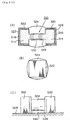
- FIG. 24 is a section showing an electronic component provided with an armor portion.
- a bobbin 510 is made up of a core 512 and rectangular flanges 514 formed at both ends of the core 512.
- An electrode 516 is formed on the sides and end of each flange 514.
- a coil 518 is wound round the core 512 has a conductor 520 protruding from opposite stripped ends thereof. Both ends of the conductor 520 are respectively bonded to the electrodes 516 by heat pressure welding or similar technology.
- a plating 522 is provided on each electrode 516 and implemented by, e.g., Ni.
- An armor in the form of a coating 524 is provided on the coil 512 by use of a paint or a resin.
- FIG. 24, (B) which is a side elevation, the coating 524 is sized great enough to protrude beyond the plating 522.
- the coating 524 is ground or otherwise machined in order to remove its portions protruding beyond the plating 522.
- the coating 524 is provided with a square section having flat sides, which can be desirably sucked.
- the flat sides enhance the stability of the assembly on a circuit board.
- the coating 524 may be ground to a position deeper than the sides of the flanges 514 in order to accurately maintain the distance between assembly and the circuit board. Grinding shown and described is a specific method of increasing the flatness may be replaced with injection molding using a metal mold.
- FIG. 24, (C) shows the electronic part mounted on a circuit board 528.
- a gap 526 exists between the coating 524 and the circuit board 528.
- the electronic part is mounted such that another part 530 is accommodated in the gap 526.
- the gap 526 is so formed as to leave some coating 524 in the vicinity of the flanges 514, as illustrated. This protects the bond between the conductor 520 of the coil 518 and the electrodes 516 from the influence of the grinding of the coating 524.
- FIG. 25, (A) and (B) An alternative example is shown in FIG. 25, (A) and (B), and relates to the ratio of the flat portion of the coating.
- (A) is a plan view while (B) is a section along line#4-#4 of (A).
- the coating should preferably be flat from the suction and stability standpoint, it does not have to be entirely flat.
- a coil 541 is wound round a core 539 having rectangular electrode portions 540 at its both ends.
- a coating 542 has sides each having a flat portion 544 whose width WP is only 30 % of the width WT of the entire side.
- the flatness refers not only to complete flatness but also to flatness with some degree of curvature.
- FIG. 25 shows another example.
- a coating 554 surrounding a coil 552 between flanges 550 has its surface roughened, i.e., formed with fine irregularities.
- the coating 554 may be implemented by a paint whose viscosity is high enough to cause the contour of the coil 552 to slightly appear on the surface of the coating 554, or (2) a filler having a preselected particle size may be mixed with the paint in order to roughen the surface of the coating 554.
- the fine irregularities of the coating 554 reduce static electricity ascribable to the rubbing of electronic parts at the time of bulk feed.
- the fine irregularities allow a minimum of displacement of the electronic part to occur when a sucking nozzle is shifted at the time of mounting.
- FIG. 25, (D) shows another example relating to a conductive paste on a circuit board, e.g., soldering.
- grooves 562 are formed in the four sides of an electrode 560.
- a conductor protruding from a coil(not shown) is bonded in any one of the grooves 562.
- Such an electronic part is positioned on a circuit board 564, as shown in FIG. 25, (D).
- solder 566 When solder 566 is applied to the electronic part, it is drawn into the grooves 562.
- the solder 566 therefore forms desirable fillets and ensures a great bonding strength even if its amount is small. This is desirable for a small size, light weight configuration. Should solder be applied to the entire electrode 560, as has been customary, the electronic part might break due to the influence of the solder.
- FIG. 26, (A) shows still another example so configured as to reduce the height of an electronic part.
- FIG. 26, (B) is a section along line #5-#5 of FIG. 26, (A).
- a bobbin has a core 572 and flanges 570 formed at both ends of the core 572.
- Each flange 570 is oblong, and the core 572 has an oval cross-section.
- Each flange 570 is formed with grooves 574 for receiving the conductor of a coil (not shown) in its sides. The longer sides of the flanges 570 are laid on a circuit board (not shown) so as to reduce the height of the electronic part.
- the shorter sides of the flanges 570 may be laid on the circuit board in order to reduce the area which the electronic part occupies. In this manner, a single electronic part is selectively usable for an application requiring a low height or an application requiring a small area.
- the core 572 having an oval cross-section guarantees a core area.
- FIG. 26, (C) shows a further example.
- a fuse 588 intervenes between an electrode 582 formed on a flange 580 and a conductor 586 protruding from a coil 584.
- the electrode 582 is implemented by a thick film, so that the fuse 588 can exhibits its function sufficiently.
- the circuitry is protected if the fuse 588 is so designed as to blow when a current greater than a preselected current flows. Because an independent fuse is not necessary, this example contributes to a small size, light weight configuration.
- the fuse 588 may be replaced with a resistor, capacitor or similar circuit element. From the mounting standpoint, grooves or similar recesses should preferably be formed in the flanges 580, so that the circuit element can be formed in any one of the grooves.
- the bobbin having the flanges at its ends may be formed by baking, e.g., ferrite or alumina.
- the electrodes formed on the flanges each consists of a thin film or a thick film of, e.g., Ag, Ag-Pd, Ag-Pt or Cu having a thickness of 1 ⁇ m to 60 ⁇ m, and a 1 ⁇ m to 10 ⁇ m thick layer of, e.g., Ni, Sn or Sn-Pb formed on the above film by plating.
- the bobbin is about 1.6mm long, about 0.8mm wide, and about 0.8mm high.
- the core positioned at the center of the bobbin has a diameter of 0.2mm to 0.7mm while the flanges each has a width of 0.2mm to 0.5mm.
Landscapes
- Engineering & Computer Science (AREA)
- Power Engineering (AREA)
- Manufacturing & Machinery (AREA)
- Microelectronics & Electronic Packaging (AREA)
- Coils Or Transformers For Communication (AREA)
Claims (13)
- Verfahren zum Herstellen einer elektronischen Komponente mit einem gewickelten Draht, folgende Schritte umfassend:dadurch gekennzeichnet, dass:Bereitstellen eines Spulenkörpers (1, 140) mit einem Kern (1a), zwei oder mehr Flanschen (1b), wobei mindestens ein Flansch an einem Ende des Kerns ist, und externen Elektroden (3) auf dem einen oder den mehreren Flanschen;Umwickeln des Kerns mit einem ummantelten Leiter (4, 142), um eine Spule (142) zu bilden, und elektrisches Verbinden der Spule mit den externen Elektroden; undBilden einer Ummantelung (144) mit einer flachen Fläche (6a) auf der Spule,der Schritt des Bildens der Ummantelung (144) umfasst, dass die Ummantelung (144) derart in Richtung zur Spule (142) gedrückt wird, dass sie in die Spalten zwischen den Windungen (154) der Spule (142) eindringt (F5).
- Verfahren nach Anspruch 1, wobei der Schritt des Bereitstellens des Spulenkörpers (1, 140) umfasst, dass ein Block (10, 22, 30, 40, 44) maschinell bearbeitet wird.
- Verfahren nach Anspruch 2, wobei der Schritt des maschinellen Bearbeitens des Blocks (10, 22) umfasst, dass Ein-(12) oder Ausbuchtungen (24) auf gegenüberliegenden Seiten des Blocks gebildet werden, und der Block durch Drehen des Blocks maschinell bearbeitet wird, wobei die Ein- oder Ausbuchtungen als Zentren benutzt werden.
- Verfahren nach Anspruch 2, wobei der Schritt des maschinellen Bearbeitens des Blocks (30) umfasst, dass Führungen (32) auf gegenüberliegenden Seiten des Blocks ausgebildet werden, und dass der Block durch Drehen des Blocks maschinell bearbeitet wird, wobei die Führungen als Zentren benutzt werden.
- Verfahren nach Anspruch 2, wobei der Schritt des maschinellen Bearbeitens des Blocks (40) umfasst, dass Ein- (42) oder Ausbuchtungen zum Halten auf Seiten des Blocks gebildet werden, und der Block durch Drehen des Blocks maschinell bearbeitet wird, wobei der Block über die Ein- oder Ausbuchtungen gehalten wird.
- Verfahren nach einem der Ansprüche 2 bis 5, wobei weiterhin Elektroden (56) auf dem Block (54) gebildet werden und ein Teil der Elektroden während des maschinellen Bearbeitens des Blocks entfernt werden.
- Verfahren nach einem der Ansprüche 1 bis 6, wobei weiterhin vor dem Wickeln der Spule (90) eine oder mehrere Kappen (84, 84A, 84B) an dem einen oder den mehreren Flanschen (85) angebracht werden, und die Kappen, nachdem die Enden der Spule (90) elektrisch mit den externen Elektroden (81) verbunden worden sind, entfernt werden.
- Verfahren nach einem der Ansprüche 1 bis 7, wobei der Schritt des Bereitstellens eines Spulenkörpers (1, 140) umfasst, dass eine Kappe (108, 124, 134) an einem Ende des Spulenkörpers als ein Flansch (1b) oder eine externe Elektrode (3) angebracht wird.
- Verfahren nach einem der Ansprüche 1 bis 8, wobei weiterhin eine Fläche des Kerns (152) aufgerauht wird.
- Verfahren nach einem der Ansprüche 1 bis 9, wobei die geformte Ummantelung (144) zwischen dem Kern (539) und jedem der Flansche (540) einen gekrümmten Teil (542) umfasst.
- Verfahren nach einem der Ansprüche 1 bis 10, wobei die externen Elektroden (3) durch eine Eintauchmethode mit einer hochviskosen Eintauchflüssigkeit (52) gebildet werden.
- Verfahren nach einem der Ansprüche 1 bis 11, wobei die Ummantelung aus einem Harz gebildet wird, und das Verfahren weiterhin umfasst, dass das Harz in mehreren aufeinanderfolgenden Schritten auf die Spule aufgebracht wird.
- Verfahren nach einem der Ansprüche 1 bis 12, wobei die Ummantelung aus einem Harz gebildet wird und das Verfahren weiterhin umfasst, dass das Harz auf die Spule (518) derart aufgebracht wird, dass das Harz (524) sich von der Oberfläche der externen Elektroden (516, 522) nach außen wölbt, und die Oberfläche des Harzes in eine vorgewählte Form gebracht wird.
Applications Claiming Priority (9)
| Application Number | Priority Date | Filing Date | Title |
|---|---|---|---|
| JP33497396A JP3319697B2 (ja) | 1996-11-29 | 1996-11-29 | 巻線型電子部品及びその製造方法 |
| JP334973/96 | 1996-11-29 | ||
| JP33497396 | 1996-11-29 | ||
| JP33482596 | 1996-11-30 | ||
| JP33482596A JP3402973B2 (ja) | 1996-11-30 | 1996-11-30 | 巻線型電子部品の製造方法 |
| JP334825/96 | 1996-11-30 | ||
| JP8352817A JPH10172853A (ja) | 1996-12-14 | 1996-12-14 | 巻線型電子部品及びその製造方法 |
| JP35281796 | 1996-12-14 | ||
| JP352817/96 | 1996-12-14 |
Publications (3)
| Publication Number | Publication Date |
|---|---|
| EP0845792A2 EP0845792A2 (de) | 1998-06-03 |
| EP0845792A3 EP0845792A3 (de) | 1999-02-10 |
| EP0845792B1 true EP0845792B1 (de) | 2004-02-11 |
Family
ID=27340694
Family Applications (1)
| Application Number | Title | Priority Date | Filing Date |
|---|---|---|---|
| EP97309130A Expired - Lifetime EP0845792B1 (de) | 1996-11-29 | 1997-11-13 | Verfahren zur Herstellung eines drahtgewickelten elektronischen Bauelements |
Country Status (4)
| Country | Link |
|---|---|
| US (3) | US6144280A (de) |
| EP (1) | EP0845792B1 (de) |
| CN (1) | CN1154127C (de) |
| DE (1) | DE69727543D1 (de) |
Cited By (1)
| Publication number | Priority date | Publication date | Assignee | Title |
|---|---|---|---|---|
| RU2603362C1 (ru) * | 2015-09-08 | 2016-11-27 | Общество с ограниченной ответственностью "АРТАКОМ" | Чип-индуктивность для автоматизированного поверхностного монтажа |
Families Citing this family (99)
| Publication number | Priority date | Publication date | Assignee | Title |
|---|---|---|---|---|
| JP3195585B2 (ja) | 1998-10-27 | 2001-08-06 | ティーディーケイ株式会社 | 表面実装自己誘導型インダクタンス部品 |
| JP4039779B2 (ja) * | 1999-01-28 | 2008-01-30 | 太陽誘電株式会社 | チップ状電子部品の製造方法 |
| JP2000269050A (ja) * | 1999-03-16 | 2000-09-29 | Taiyo Yuden Co Ltd | コモンモードチョークコイル |
| US6437676B1 (en) * | 1999-06-29 | 2002-08-20 | Matsushita Electric Industrial Co., Ltd. | Inductance element |
| JP2001052937A (ja) | 1999-08-13 | 2001-02-23 | Murata Mfg Co Ltd | インダクタ及びその製造方法 |
| JP3617426B2 (ja) * | 1999-09-16 | 2005-02-02 | 株式会社村田製作所 | インダクタ及びその製造方法 |
| JP3710042B2 (ja) * | 1999-09-20 | 2005-10-26 | Tdk株式会社 | コモンモードフィルタ |
| JP3456454B2 (ja) * | 1999-09-30 | 2003-10-14 | 株式会社村田製作所 | ワイヤを有する電子部品 |
| JP3583965B2 (ja) * | 1999-11-26 | 2004-11-04 | 太陽誘電株式会社 | 面実装型コイル及びその製造方法 |
| GB2361110A (en) * | 2000-04-03 | 2001-10-10 | Abb Ab | An induction device |
| US6918173B2 (en) * | 2000-07-31 | 2005-07-19 | Ceratech Corporation | Method for fabricating surface mountable chip inductor |
| AU2001286255A1 (en) * | 2000-09-14 | 2002-03-26 | Matsushita Electric Works Ltd. | Electromagnetic device and high-voltage generating device and method of producing electromagnetic device |
| JP3582477B2 (ja) * | 2000-11-01 | 2004-10-27 | 株式会社村田製作所 | 電子部品及びその製造方法 |
| US6946758B2 (en) | 2001-01-09 | 2005-09-20 | Black & Decker Inc. | Dynamoelectric machine having encapsulated coil structure with one or more of phase change additives, insert molded features and insulated pinion |
| US7096566B2 (en) * | 2001-01-09 | 2006-08-29 | Black & Decker Inc. | Method for making an encapsulated coil structure |
| US7814641B2 (en) | 2001-01-09 | 2010-10-19 | Black & Decker Inc. | Method of forming a power tool |
| CZ20031901A3 (cs) | 2001-01-09 | 2003-11-12 | Black & Decker Inc. | Elektrický motor s kotvou potaženou tepelně vodivým plastem |
| DE10105416A1 (de) * | 2001-01-30 | 2002-08-14 | Siemens Ag | Spule |
| MXPA04010749A (es) * | 2002-04-29 | 2005-07-05 | Quelis Id Systems Inc | Configuracion de espiral para dispositivos de identificacion de radiofrecuencia, proceso y aparato para fabricar esta configuracion. |
| TW553465U (en) * | 2002-07-25 | 2003-09-11 | Micro Star Int Co Ltd | Integrated inductor |
| TW559321U (en) * | 2002-12-10 | 2003-10-21 | Ferrico Corp | Device structure for sensing magnetism |
| JP4354187B2 (ja) * | 2003-01-21 | 2009-10-28 | Tdk株式会社 | 高qヘリカルコイルチップおよびその製造方法 |
| US6778055B1 (en) * | 2003-02-07 | 2004-08-17 | Aoba Technology Co., Ltd. | Core member for winding |
| JP4412702B2 (ja) * | 2003-03-28 | 2010-02-10 | スミダコーポレーション株式会社 | インダクタンス素子 |
| US7212093B2 (en) * | 2003-07-25 | 2007-05-01 | Kyocera Corporation | Ferrite core, method of manufacturing the same, and common-mode noise filter using the same |
| JP4532167B2 (ja) * | 2003-08-21 | 2010-08-25 | コーア株式会社 | チップコイルおよびチップコイルを実装した基板 |
| DE20318052U1 (de) * | 2003-11-21 | 2004-03-04 | Neosid Pemetzrieder Gmbh & Co Kg | Induktives Miniatur-Bauelement für SMD-Montage |
| DE10356094A1 (de) * | 2003-12-01 | 2005-07-14 | Siemens Audiologische Technik Gmbh | Induktionsspule mit Querempfindlichkeit für Hörgeräte |
| JP2005210055A (ja) * | 2003-12-22 | 2005-08-04 | Taiyo Yuden Co Ltd | 面実装コイル部品及びその製造方法 |
| JP2005327876A (ja) * | 2004-05-13 | 2005-11-24 | Tdk Corp | コイル部品及びその製造方法 |
| US7612641B2 (en) * | 2004-09-21 | 2009-11-03 | Pulse Engineering, Inc. | Simplified surface-mount devices and methods |
| JP2006100697A (ja) * | 2004-09-30 | 2006-04-13 | Chuki Seiki Kk | ノイズ除去デバイス |
| JP2006100700A (ja) * | 2004-09-30 | 2006-04-13 | Chuki Seiki Kk | ノイズ除去デバイス |
| DE102004058452A1 (de) * | 2004-12-03 | 2006-06-08 | Vacuumschmelze Gmbh & Co. Kg | Stromerfassungseinrichtung und Verfahren zum Herstellen einer solchen Stromerfassungseinrichtung |
| DE102005022927A1 (de) * | 2005-05-13 | 2006-11-16 | Würth Elektronik iBE GmbH | Elektronisches Bauteil und Verfahren zu seiner Befestigung |
| JP4844045B2 (ja) * | 2005-08-18 | 2011-12-21 | Tdk株式会社 | 電子部品及びその製造方法 |
| JP4947431B2 (ja) * | 2005-11-09 | 2012-06-06 | 株式会社村田製作所 | 固体電解コンデンサ及びその製造方法 |
| US8174820B2 (en) * | 2005-11-09 | 2012-05-08 | Murata Manufacturing Co., Ltd. | Solid electrolytic capacitor and method for manufacturing same |
| JP4780111B2 (ja) * | 2005-11-22 | 2011-09-28 | 株式会社村田製作所 | 巻線型コイル |
| CN1794376B (zh) * | 2006-01-06 | 2010-05-12 | 浙江大学 | 带有溅射膜电极的电感骨架及其生产方法 |
| JP2007311622A (ja) * | 2006-05-19 | 2007-11-29 | Toko Inc | 小型面実装電子部品とその製造方法 |
| JP2008053670A (ja) * | 2006-08-25 | 2008-03-06 | Taiyo Yuden Co Ltd | ドラム型コアを用いたインダクタ及びドラム型コアを用いたインダクタの製造方法 |
| US7855625B2 (en) * | 2006-08-31 | 2010-12-21 | General Electric Company | Lamp transformer |
| EP1895549B1 (de) * | 2006-09-01 | 2015-04-15 | DET International Holding Limited | Induktives Bauelement |
| JP5122783B2 (ja) * | 2006-09-28 | 2013-01-16 | 三洋電機株式会社 | コイン型電池 |
| DE102007017702A1 (de) * | 2007-04-14 | 2008-10-16 | Abb Technology Ag | Elektrisches Bauteil mit Wicklung und Anzapfung |
| TWI405225B (zh) * | 2008-02-22 | 2013-08-11 | Cyntec Co Ltd | 扼流線圈 |
| WO2009148072A1 (ja) * | 2008-06-05 | 2009-12-10 | コーア株式会社 | チップインダクタおよびその製造方法 |
| DE102008030631A1 (de) * | 2008-06-24 | 2009-12-31 | Würth Elektronik iBE GmbH | Elektronisches Bauelement |
| US9208937B2 (en) | 2009-02-27 | 2015-12-08 | Cyntec Co., Ltd. | Choke having a core with a pillar having a non-circular and non-rectangular cross section |
| USRE48472E1 (en) | 2009-02-27 | 2021-03-16 | Cyntec Co., Ltd. | Choke having a core with a pillar having a non-circular and non-rectangular cross section |
| US9117580B2 (en) * | 2009-02-27 | 2015-08-25 | Cyntec Co., Ltd. | Choke |
| TWI436381B (zh) * | 2009-06-08 | 2014-05-01 | Cyntec Co Ltd | 扼流器 |
| CN102034593B (zh) * | 2009-09-25 | 2012-09-26 | 川部股份有限公司 | 电感及其制造方法 |
| CN102110512A (zh) * | 2010-12-24 | 2011-06-29 | 柏玉新 | 带基座软磁铁氧体磁环 |
| JP2012160507A (ja) * | 2011-01-31 | 2012-08-23 | Toko Inc | 面実装インダクタと面実装インダクタの製造方法 |
| CN102231323A (zh) * | 2011-04-21 | 2011-11-02 | 广州市麦新电子有限公司 | 超小型电感的制造工艺 |
| WO2013065183A1 (ja) * | 2011-11-04 | 2013-05-10 | トヨタ自動車株式会社 | リアクトルおよびその製造方法 |
| TWI466144B (zh) * | 2011-12-20 | 2014-12-21 | Cyntec Co Ltd | 扼流器 |
| US10614945B2 (en) * | 2011-12-20 | 2020-04-07 | Cyntec Co., Ltd. | Choke having a core with a pillar having a non-circular and non-rectangular cross section |
| CN102723161B (zh) * | 2012-07-09 | 2013-12-04 | 中国科学院电工研究所 | 一种陶瓷骨架超导磁体螺线管线圈 |
| CN102723162B (zh) * | 2012-07-09 | 2013-12-04 | 中国科学院电工研究所 | 一种不锈钢骨架Nb3Sn超导磁体螺线管线圈 |
| CN102945728A (zh) * | 2012-11-06 | 2013-02-27 | 杭州康磁电子有限公司 | 一种高温焊接溅射电感骨架 |
| DE102013101364B4 (de) * | 2013-02-12 | 2023-02-02 | Tdk Electronics Ag | Elektrisches Übertragerbauelement |
| JP6377336B2 (ja) * | 2013-03-06 | 2018-08-22 | 株式会社東芝 | インダクタ及びその製造方法 |
| CN106409477A (zh) * | 2013-03-25 | 2017-02-15 | 乾坤科技股份有限公司 | 电感器 |
| JP5894114B2 (ja) * | 2013-05-17 | 2016-03-23 | 東光株式会社 | 面実装インダクタの製造方法 |
| JP5998110B2 (ja) | 2013-08-02 | 2016-09-28 | Ckd株式会社 | 電磁コイル、電磁コイルの製造方法、及び電磁アクチュエータ |
| JP6360288B2 (ja) | 2013-09-04 | 2018-07-18 | Ckd株式会社 | 電磁コイルの冷却構造、及び電磁アクチュエータ |
| JP6255933B2 (ja) * | 2013-11-20 | 2018-01-10 | Tdk株式会社 | コイル装置 |
| US9653205B2 (en) * | 2014-04-30 | 2017-05-16 | Cyntec Co., Ltd. | Electrode structure and the corresponding electrical component using the same and the fabrication method thereof |
| JP6435649B2 (ja) * | 2014-06-05 | 2018-12-12 | Tdk株式会社 | コイル部品及びその製造方法 |
| US9831023B2 (en) * | 2014-07-10 | 2017-11-28 | Cyntec Co., Ltd. | Electrode structure and the corresponding electrical component using the same and the fabrication method thereof |
| JP6522297B2 (ja) | 2014-07-28 | 2019-05-29 | 太陽誘電株式会社 | コイル部品 |
| JP6502627B2 (ja) * | 2014-07-29 | 2019-04-17 | 太陽誘電株式会社 | コイル部品及び電子機器 |
| JP6316136B2 (ja) * | 2014-08-01 | 2018-04-25 | 太陽誘電株式会社 | コイル部品およびそれを備える電子機器 |
| CN106663531B (zh) * | 2014-08-19 | 2018-04-06 | 株式会社村田制作所 | 卷线型线圈部件的制造方法 |
| KR101627134B1 (ko) * | 2014-09-23 | 2016-06-03 | 삼성전기주식회사 | 공통 모드 필터 |
| JP6247629B2 (ja) | 2014-12-11 | 2017-12-13 | Ckd株式会社 | コイル用シートの製造方法、及びコイルの製造方法 |
| JP6352791B2 (ja) | 2014-12-11 | 2018-07-04 | Ckd株式会社 | コイル用シート、コイル、及びコイルの製造方法 |
| US9899131B2 (en) * | 2015-07-20 | 2018-02-20 | Cyntec Co., Ltd. | Structure of an electronic component and an inductor |
| KR20170023501A (ko) * | 2015-08-24 | 2017-03-06 | 삼성전기주식회사 | 코일 전자부품 및 그 제조방법 |
| JP6451654B2 (ja) * | 2016-01-07 | 2019-01-16 | 株式会社村田製作所 | コイル部品 |
| CN105469956A (zh) * | 2016-02-17 | 2016-04-06 | 德州信平电子有限公司 | 电源变压器引线焊接结构及其焊接工艺 |
| JP6477592B2 (ja) * | 2016-05-13 | 2019-03-06 | 株式会社村田製作所 | セラミックコア、巻線型電子部品及びセラミックコアの製造方法 |
| JP6627731B2 (ja) * | 2016-12-01 | 2020-01-08 | 株式会社村田製作所 | 巻線型コイル部品及び巻線型コイル部品の製造方法 |
| CN106783017A (zh) * | 2016-12-29 | 2017-05-31 | 广东小天才科技有限公司 | 电感器及电感器的制造方法 |
| US10998613B2 (en) * | 2017-03-23 | 2021-05-04 | Wits Co., Ltd. | Chip antenna |
| JP6686978B2 (ja) * | 2017-06-24 | 2020-04-22 | 株式会社村田製作所 | コイル部品およびその製造方法 |
| JP6959062B2 (ja) | 2017-08-02 | 2021-11-02 | 太陽誘電株式会社 | コイル部品 |
| JP7020363B2 (ja) * | 2018-02-05 | 2022-02-16 | 株式会社村田製作所 | コモンモードチョークコイル |
| US11837396B2 (en) * | 2018-02-05 | 2023-12-05 | Murata Manufacturing Co., Ltd. | Common-mode choke coil |
| CN110970216B (zh) * | 2018-09-28 | 2021-04-02 | 德宙佑电股份有限公司 | 电感专用机的绞线机构 |
| JP7288297B2 (ja) | 2018-10-30 | 2023-06-07 | 太陽誘電株式会社 | コイル部品及び電子機器 |
| JP7183934B2 (ja) * | 2019-04-22 | 2022-12-06 | Tdk株式会社 | コイル部品及びその製造方法 |
| JP7146178B2 (ja) * | 2019-05-24 | 2022-10-04 | 株式会社オートネットワーク技術研究所 | リアクトル |
| JP6956925B2 (ja) * | 2019-05-24 | 2021-11-02 | 三菱電機株式会社 | ノイズ低減素子 |
| JP7463837B2 (ja) | 2020-05-14 | 2024-04-09 | Tdk株式会社 | 電子部品 |
| CN113674968B (zh) * | 2020-05-14 | 2025-01-28 | Tdk株式会社 | 电子部件 |
Family Cites Families (34)
| Publication number | Priority date | Publication date | Assignee | Title |
|---|---|---|---|---|
| US3585553A (en) * | 1970-04-16 | 1971-06-15 | Us Army | Microminiature leadless inductance element |
| JPS51115547A (en) * | 1975-04-03 | 1976-10-12 | Ig Kogyo Kk | Apparafus for spreading granular substances |
| US4316923A (en) * | 1975-04-14 | 1982-02-23 | Ampex Corporation | Precision dielectric filled ferrite toroid for use in microwave devices |
| JPS53126833A (en) | 1977-04-13 | 1978-11-06 | Hitachi Ltd | Terminal control system |
| JPS56110612A (en) * | 1980-02-08 | 1981-09-01 | Yamanouchi Pharmaceut Co Ltd | Readily disintegrable and absorbable compression molded article of slightly soluble drug |
| JPS5773916A (en) * | 1980-10-24 | 1982-05-08 | Tdk Corp | Small-sized inductor and preparation thereof |
| DE3042433A1 (de) * | 1980-11-11 | 1982-07-01 | Draloric Electronic GmbH, 8500 Nürnberg | Induktives bauelement zum einsatz in gedruckte schaltungen |
| JPS5793115A (en) * | 1980-12-02 | 1982-06-10 | Koatsu Kako Kk | Production of decorative article |
| JPS5875825A (ja) * | 1981-10-29 | 1983-05-07 | Murata Mfg Co Ltd | チツプインダクタの製造方法 |
| FR2548821B1 (fr) * | 1983-07-04 | 1986-01-24 | Europ Composants Electron | Composant electronique inductif pour le report a plat |
| JPS60109313A (ja) * | 1983-11-17 | 1985-06-14 | Mitsubishi Electric Corp | 中間周波処理用半導体集積回路 |
| US4704592A (en) * | 1984-09-13 | 1987-11-03 | Siemens Aktiengesellschaft | Chip inductor electronic component |
| JPS61144616A (ja) * | 1984-12-18 | 1986-07-02 | Olympus Optical Co Ltd | 明るい広角レンズ |
| US4696100A (en) * | 1985-02-21 | 1987-09-29 | Matsushita Electric Industrial Co., Ltd. | Method of manufacturing a chip coil |
| JPH0683706B2 (ja) * | 1985-03-04 | 1994-10-26 | 之男 斎藤 | 姿勢制御機能診断装置 |
| JPS625618A (ja) * | 1985-07-02 | 1987-01-12 | Matsushita Electric Ind Co Ltd | チツプ・インダクタ |
| JPS62190322A (ja) | 1986-02-18 | 1987-08-20 | Rinnai Corp | 燃焼制御装置 |
| JPS62286211A (ja) * | 1986-06-05 | 1987-12-12 | Murata Mfg Co Ltd | チツプコイル |
| US4810983A (en) * | 1986-12-22 | 1989-03-07 | Murata Manufacturing Co., Ltd. | Chip type LC composite component |
| JP2592505B2 (ja) | 1988-09-29 | 1997-03-19 | 株式会社クボタ | 杭打設工法 |
| JP2688429B2 (ja) | 1988-09-29 | 1997-12-10 | マミヤ・オーピー株式会社 | モータロック金庫 |
| US4842352A (en) * | 1988-10-05 | 1989-06-27 | Tdk Corporation | Chip-like inductance element |
| WO1990013135A1 (en) * | 1989-04-21 | 1990-11-01 | Motorola, Inc. | Improved surface-mountable air core inductor |
| JPH04364009A (ja) | 1991-06-11 | 1992-12-16 | Murata Mfg Co Ltd | 巻線型インダクタ |
| JPH0577909A (ja) | 1991-09-20 | 1993-03-30 | Toshiba Corp | 倉庫の搬出入装置 |
| JPH0737720A (ja) | 1993-07-21 | 1995-02-07 | Hitachi Metals Ltd | チップ部品及びその使用方法 |
| JPH07192924A (ja) | 1993-12-27 | 1995-07-28 | Fuji Elelctrochem Co Ltd | 巻線部品のフェライトコア |
| JPH07192931A (ja) | 1993-12-27 | 1995-07-28 | Taiyo Yuden Co Ltd | コイル部品 |
| JPH07220948A (ja) | 1994-02-04 | 1995-08-18 | Matsushita Electric Ind Co Ltd | チップインダクタンス部品およびその製造方法 |
| JPH08124761A (ja) * | 1994-10-19 | 1996-05-17 | Taiyo Yuden Co Ltd | チップ形インダクタおよびその製造方法 |
| JPH08264343A (ja) | 1995-03-22 | 1996-10-11 | Matsushita Electric Ind Co Ltd | チップコモンモードチョークおよびその製造方法 |
| JPH08273964A (ja) * | 1995-03-30 | 1996-10-18 | Citizen Watch Co Ltd | 電子時計用ステップモ−タのコイル巻芯の製造方法 |
| JPH08298359A (ja) | 1995-04-26 | 1996-11-12 | Kyocera Corp | 銅厚膜回路基板 |
| JPH08264384A (ja) | 1996-04-16 | 1996-10-11 | Rohm Co Ltd | チップ型複合電子部品 |
-
1997
- 1997-11-10 US US08/967,786 patent/US6144280A/en not_active Expired - Lifetime
- 1997-11-13 EP EP97309130A patent/EP0845792B1/de not_active Expired - Lifetime
- 1997-11-13 DE DE69727543T patent/DE69727543D1/de not_active Expired - Lifetime
- 1997-11-14 CN CNB971141355A patent/CN1154127C/zh not_active Expired - Fee Related
-
2000
- 2000-09-19 US US09/664,720 patent/US6449830B1/en not_active Expired - Fee Related
-
2002
- 2002-08-28 US US10/229,074 patent/US6727792B2/en not_active Expired - Fee Related
Cited By (1)
| Publication number | Priority date | Publication date | Assignee | Title |
|---|---|---|---|---|
| RU2603362C1 (ru) * | 2015-09-08 | 2016-11-27 | Общество с ограниченной ответственностью "АРТАКОМ" | Чип-индуктивность для автоматизированного поверхностного монтажа |
Also Published As
| Publication number | Publication date |
|---|---|
| US6727792B2 (en) | 2004-04-27 |
| US6144280A (en) | 2000-11-07 |
| EP0845792A2 (de) | 1998-06-03 |
| US6449830B1 (en) | 2002-09-17 |
| CN1154127C (zh) | 2004-06-16 |
| EP0845792A3 (de) | 1999-02-10 |
| DE69727543D1 (de) | 2004-03-18 |
| CN1187014A (zh) | 1998-07-08 |
| US20020190832A1 (en) | 2002-12-19 |
Similar Documents
| Publication | Publication Date | Title |
|---|---|---|
| EP0845792B1 (de) | Verfahren zur Herstellung eines drahtgewickelten elektronischen Bauelements | |
| US6535095B2 (en) | Wound type common mode choke coil | |
| EP0206584B1 (de) | Elektronische Vorrichtung für Flachmontage | |
| CN113871161B (zh) | 线圈部件 | |
| US4842352A (en) | Chip-like inductance element | |
| JPH0888124A (ja) | インダクタンス素子とその製造方法 | |
| KR102745210B1 (ko) | 코일 부품 및 전자 기기 | |
| CN111128513B (zh) | 线圈部件和电子器件 | |
| KR960005687B1 (ko) | 평코일 및 그 제조 방법 | |
| US4553123A (en) | Miniature inductor | |
| CA2274165C (en) | Method of manufacturing bead inductor and the bead inductor produced thereby | |
| JP3402973B2 (ja) | 巻線型電子部品の製造方法 | |
| US6437676B1 (en) | Inductance element | |
| GB2032810A (en) | Manufacture of coreless armatures | |
| JP3319697B2 (ja) | 巻線型電子部品及びその製造方法 | |
| JPH10172853A (ja) | 巻線型電子部品及びその製造方法 | |
| KR19980042442A (ko) | 코일형 전자부품 및 그 제조방법 | |
| JP2002313629A (ja) | チップ型インダクタ | |
| JPH09306744A (ja) | チップ状インダクタ | |
| CN116206852B (zh) | 线圈部件 | |
| JP3051534B2 (ja) | チップインダクタ | |
| US20260066182A1 (en) | Coil component | |
| JPH0512975Y2 (de) | ||
| JPH10294223A (ja) | チップインダクタ | |
| JP2805375B2 (ja) | 磁気シールド型インダクタの製造方法 |
Legal Events
| Date | Code | Title | Description |
|---|---|---|---|
| PUAI | Public reference made under article 153(3) epc to a published international application that has entered the european phase |
Free format text: ORIGINAL CODE: 0009012 |
|
| AK | Designated contracting states |
Kind code of ref document: A2 Designated state(s): DE FR GB |
|
| AX | Request for extension of the european patent |
Free format text: AL;LT;LV;MK;RO;SI |
|
| PUAL | Search report despatched |
Free format text: ORIGINAL CODE: 0009013 |
|
| AK | Designated contracting states |
Kind code of ref document: A3 Designated state(s): AT BE CH DE DK ES FI FR GB GR IE IT LI LU MC NL PT SE |
|
| AX | Request for extension of the european patent |
Free format text: AL;LT;LV;MK;RO;SI |
|
| 17P | Request for examination filed |
Effective date: 19990806 |
|
| AKX | Designation fees paid |
Free format text: DE FR GB |
|
| 17Q | First examination report despatched |
Effective date: 20011129 |
|
| RTI1 | Title (correction) |
Free format text: METHOD OF MANUFACTURING A WIRE WOUND ELECTRONIC COMPONENT |
|
| GRAH | Despatch of communication of intention to grant a patent |
Free format text: ORIGINAL CODE: EPIDOS IGRA |
|
| GRAS | Grant fee paid |
Free format text: ORIGINAL CODE: EPIDOSNIGR3 |
|
| GRAA | (expected) grant |
Free format text: ORIGINAL CODE: 0009210 |
|
| AK | Designated contracting states |
Kind code of ref document: B1 Designated state(s): DE FR GB |
|
| PG25 | Lapsed in a contracting state [announced via postgrant information from national office to epo] |
Ref country code: FR Free format text: LAPSE BECAUSE OF FAILURE TO SUBMIT A TRANSLATION OF THE DESCRIPTION OR TO PAY THE FEE WITHIN THE PRESCRIBED TIME-LIMIT Effective date: 20040211 |
|
| REG | Reference to a national code |
Ref country code: GB Ref legal event code: FG4D |
|
| REF | Corresponds to: |
Ref document number: 69727543 Country of ref document: DE Date of ref document: 20040318 Kind code of ref document: P |
|
| PG25 | Lapsed in a contracting state [announced via postgrant information from national office to epo] |
Ref country code: DE Free format text: LAPSE BECAUSE OF FAILURE TO SUBMIT A TRANSLATION OF THE DESCRIPTION OR TO PAY THE FEE WITHIN THE PRESCRIBED TIME-LIMIT Effective date: 20040512 |
|
| PLBE | No opposition filed within time limit |
Free format text: ORIGINAL CODE: 0009261 |
|
| STAA | Information on the status of an ep patent application or granted ep patent |
Free format text: STATUS: NO OPPOSITION FILED WITHIN TIME LIMIT |
|
| EN | Fr: translation not filed | ||
| 26N | No opposition filed |
Effective date: 20041112 |
|
| PGFP | Annual fee paid to national office [announced via postgrant information from national office to epo] |
Ref country code: GB Payment date: 20081117 Year of fee payment: 12 |
|
| GBPC | Gb: european patent ceased through non-payment of renewal fee |
Effective date: 20091113 |
|
| PG25 | Lapsed in a contracting state [announced via postgrant information from national office to epo] |
Ref country code: GB Free format text: LAPSE BECAUSE OF NON-PAYMENT OF DUE FEES Effective date: 20091113 |