EP0892441A2 - Feldeffekttransistor mit versenktem Gate und Verfahren zur Herstellung - Google Patents
Feldeffekttransistor mit versenktem Gate und Verfahren zur Herstellung Download PDFInfo
- Publication number
- EP0892441A2 EP0892441A2 EP98110701A EP98110701A EP0892441A2 EP 0892441 A2 EP0892441 A2 EP 0892441A2 EP 98110701 A EP98110701 A EP 98110701A EP 98110701 A EP98110701 A EP 98110701A EP 0892441 A2 EP0892441 A2 EP 0892441A2
- Authority
- EP
- European Patent Office
- Prior art keywords
- layer
- active layer
- semiconductor layer
- recess
- field effect
- Prior art date
- Legal status (The legal status is an assumption and is not a legal conclusion. Google has not performed a legal analysis and makes no representation as to the accuracy of the status listed.)
- Granted
Links
- 230000005669 field effect Effects 0.000 title claims abstract description 49
- 238000000034 method Methods 0.000 title claims abstract description 35
- 238000004519 manufacturing process Methods 0.000 title description 7
- 229910000980 Aluminium gallium arsenide Inorganic materials 0.000 claims abstract description 27
- 238000005530 etching Methods 0.000 claims abstract description 25
- 239000000758 substrate Substances 0.000 claims abstract description 17
- 239000004065 semiconductor Substances 0.000 claims description 41
- 229910001218 Gallium arsenide Inorganic materials 0.000 claims description 30
- 229910000530 Gallium indium arsenide Inorganic materials 0.000 claims description 3
- 239000000463 material Substances 0.000 claims description 3
- 239000010410 layer Substances 0.000 claims 61
- NBIIXXVUZAFLBC-UHFFFAOYSA-N Phosphoric acid Chemical compound OP(O)(O)=O NBIIXXVUZAFLBC-UHFFFAOYSA-N 0.000 claims 2
- 239000011241 protective layer Substances 0.000 claims 2
- 229910000147 aluminium phosphate Inorganic materials 0.000 claims 1
- 230000015556 catabolic process Effects 0.000 abstract description 7
- KRKNYBCHXYNGOX-UHFFFAOYSA-N citric acid Chemical compound OC(=O)CC(O)(C(O)=O)CC(O)=O KRKNYBCHXYNGOX-UHFFFAOYSA-N 0.000 description 4
- 241001125929 Trisopterus luscus Species 0.000 description 3
- 238000000206 photolithography Methods 0.000 description 3
- KLZUFWVZNOTSEM-UHFFFAOYSA-K Aluminium flouride Chemical compound F[Al](F)F KLZUFWVZNOTSEM-UHFFFAOYSA-K 0.000 description 2
- VYPSYNLAJGMNEJ-UHFFFAOYSA-N Silicium dioxide Chemical compound O=[Si]=O VYPSYNLAJGMNEJ-UHFFFAOYSA-N 0.000 description 2
- 238000005229 chemical vapour deposition Methods 0.000 description 2
- 238000004140 cleaning Methods 0.000 description 2
- 230000008020 evaporation Effects 0.000 description 2
- 238000001704 evaporation Methods 0.000 description 2
- 239000012212 insulator Substances 0.000 description 2
- 239000000203 mixture Substances 0.000 description 2
- 229910015844 BCl3 Inorganic materials 0.000 description 1
- MHAJPDPJQMAIIY-UHFFFAOYSA-N Hydrogen peroxide Chemical compound OO MHAJPDPJQMAIIY-UHFFFAOYSA-N 0.000 description 1
- 229910052681 coesite Inorganic materials 0.000 description 1
- 238000010276 construction Methods 0.000 description 1
- 238000007796 conventional method Methods 0.000 description 1
- 229910052906 cristobalite Inorganic materials 0.000 description 1
- 230000003247 decreasing effect Effects 0.000 description 1
- 230000006866 deterioration Effects 0.000 description 1
- 238000009826 distribution Methods 0.000 description 1
- 239000007789 gas Substances 0.000 description 1
- 238000012986 modification Methods 0.000 description 1
- 230000004048 modification Effects 0.000 description 1
- 238000007254 oxidation reaction Methods 0.000 description 1
- 150000003016 phosphoric acids Chemical class 0.000 description 1
- 239000000377 silicon dioxide Substances 0.000 description 1
- 229910052682 stishovite Inorganic materials 0.000 description 1
- FAQYAMRNWDIXMY-UHFFFAOYSA-N trichloroborane Chemical compound ClB(Cl)Cl FAQYAMRNWDIXMY-UHFFFAOYSA-N 0.000 description 1
- 229910052905 tridymite Inorganic materials 0.000 description 1
- 238000001039 wet etching Methods 0.000 description 1
Images


Classifications
-
- H—ELECTRICITY
- H10—SEMICONDUCTOR DEVICES; ELECTRIC SOLID-STATE DEVICES NOT OTHERWISE PROVIDED FOR
- H10D—INORGANIC ELECTRIC SEMICONDUCTOR DEVICES
- H10D30/00—Field-effect transistors [FET]
- H10D30/01—Manufacture or treatment
- H10D30/061—Manufacture or treatment of FETs having Schottky gates
- H10D30/0612—Manufacture or treatment of FETs having Schottky gates of lateral single-gate Schottky FETs
-
- H—ELECTRICITY
- H10—SEMICONDUCTOR DEVICES; ELECTRIC SOLID-STATE DEVICES NOT OTHERWISE PROVIDED FOR
- H10D—INORGANIC ELECTRIC SEMICONDUCTOR DEVICES
- H10D30/00—Field-effect transistors [FET]
- H10D30/01—Manufacture or treatment
- H10D30/015—Manufacture or treatment of FETs having heterojunction interface channels or heterojunction gate electrodes, e.g. HEMT
-
- H—ELECTRICITY
- H10—SEMICONDUCTOR DEVICES; ELECTRIC SOLID-STATE DEVICES NOT OTHERWISE PROVIDED FOR
- H10D—INORGANIC ELECTRIC SEMICONDUCTOR DEVICES
- H10D30/00—Field-effect transistors [FET]
- H10D30/80—FETs having rectifying junction gate electrodes
- H10D30/87—FETs having Schottky gate electrodes, e.g. metal-semiconductor FETs [MESFET]
- H10D30/877—FETs having Schottky gate electrodes, e.g. metal-semiconductor FETs [MESFET] having recessed gate electrodes
-
- Y—GENERAL TAGGING OF NEW TECHNOLOGICAL DEVELOPMENTS; GENERAL TAGGING OF CROSS-SECTIONAL TECHNOLOGIES SPANNING OVER SEVERAL SECTIONS OF THE IPC; TECHNICAL SUBJECTS COVERED BY FORMER USPC CROSS-REFERENCE ART COLLECTIONS [XRACs] AND DIGESTS
- Y10—TECHNICAL SUBJECTS COVERED BY FORMER USPC
- Y10S—TECHNICAL SUBJECTS COVERED BY FORMER USPC CROSS-REFERENCE ART COLLECTIONS [XRACs] AND DIGESTS
- Y10S438/00—Semiconductor device manufacturing: process
- Y10S438/97—Specified etch stop material
Definitions
- the invention relates to a field effect transistor and a method for manufacturing the same, and especially to a GaAs field effect transistor, which generates high output power and is required to be highly reliable, and a method for manufacturing the same.
- a GaAs field effect transistor provided with a double recess attracts attentions of electronic engineers as a device, which generates a high output power and withstands a high voltage applied thereto.
- the double recess is composed of a wide recess and a narrow recess, each having a form of a step of stairs, and formed by etching GaAs in most cases.
- it is indispensable to form the wide and narrow recesses with high accuracy.
- GaAs active layers and thin AlGaAs etching stopper layers are grown alternately and successively on a GaAs substrate, and the double recess is formed by selectively etching the aforementioned multilayered semiconductor.
- the double recess can be exactly formed because of the presence of the etching stopper layers, and a drain current, a threshold voltage and a gate breakdown voltage of the field effect transistor can be stabilized.
- a AlGaAs etching stopper layer is exposed on the wide recess.
- the etching stopper layer is easily oxidized, and surface state levels arise therein, which bring about the fluctuations of the characteristics of the field effect transistors. It is extremely desirable to remove the etching stopper exposed on the wide recess.
- a field effect transistor comprises:
- a method for fabricating a field effect transistor comprises the steps of:
- FIG.1 shows a cross-sectional view of the aforementioned example.
- a 300 to 500nm thick n-GaAs active layer is grown on a GaAs substrate 1.
- two 5.0 to 20nm thick AlGaAs layers serving as stopper layers are respectively grown at positions, which are respectively 50 to 150nm and 100 to 250nm high above the top surface of the GaAs substrate.
- the 50 to 150nm thick active layer 2 the 5.0 to 20nm thick stopper layer 13, the 45 to 80nm thick active layer 14, the 5.0 to 20nm thick stopper layer 15 and the 195 to 230nm thick active layer 16 are grown epitaxially and successively on the GaAs substrate 1.
- a source electrode 11 and a drain electrode 12 are formed on the active layer 16 by photolithography and lift-off technique.
- wet etching of the active layer is carried out by using the aforementioned resist pattern as a mask.
- a part of the active layer is selectively etched using enchant with low solubility on the stopper layer (mixture of citric acid and hydrogen peroxide solution, for example).
- the wide recess 18 can be formed by this process.
- the resist pattern is removed, and another resist pattern for forming a narrow recess is formed.
- the stopper layer is anisotropically etched and the active layer is exposed. Furthermore, only a part of the active layer is selectively recess etched by using the aforementioned etchant having low solubility on the stopper layer. The recess 19 is formed by this process. Thereafter, using a resist pattern as a mask, a gate electrode is formed by evaporation lift-off technique, and the resist pattern is removed. In this way, the gate electrode 20 is formed on the top surface of the stopper layer 13 in the narrow recess 19. According to the aforementioned fabrication process, the fluctuations of the shapes of the wide and narrow recesses of the field effect transistors can be suppressed, and drain currents, threshold voltages and withstand voltages of the field effect transistors can be stabilized.
- the AlGaAs layer which was used as the etching stopper layer, is exposed to the air after GaAs/AlGaAs selective etching for forming the wide recess. Since the AlGaAs layer is easily oxidized, when the AlGaAs layer makes up the surface of the wide recess, the surface state levels are arisen therein. The surface state levels become the causes of a increased gate leakage current, a decreased gate breakdown voltage, the increased standard deviation of DC characteristics of the field effect transistors fabricated from the same wafer and deterioration of high frequency characteristics.
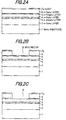
- FIGs.2A to 5 are cross-sectional views for shown fabrication process of a field effect transistor according to the first preferred embodiment of the invention.
- a n-GaAs active layer 2 is grown on a GaAs substrate 1 as the first active layer, and at a point of time that the n-GaAs active layer 2 becomes 100-250nm thick, a n-AlGaAs layer 3, which serves as a etching stopper layer in case that a narrow recess is formed, is grown till it becomes 5.0 to 10nm thick.
- a 5.0 to 100nm thick n-GaAs layer 4 is grown as the second active layer on the n-AlGaAs layer 3, on which a n-AlGaAs layer 5 is grown till it be comes about 4.0 to 10nm (4.0 to 5.0nm desirably) thick.
- a n-GaAs layer 6 is epitaxially grown as the third active layer 6 on the n-AlGaAs layer 5.
- a resist 7a is patterned in a shape of a aperture of a wide recess by photolithography in order to form the wide recess, which corresponds to the first step of the double recess.
- n-GaAs layer 6 which is not covered with the resist 7a, is selectively dry-etched by SF 6 /BCl 3 mixture gas.
- an AlGaAs layer 5 serving as an etching stopper is over-etched.
- the etch of the n-GaAs layer 6 and the same of the n-AlGaAs layer 5 are in the ratio 100:1, but the n-AlGaAs layer 5 is etched by 1 to 10nm because of the aforementioned over etch.
- the damaged layer is formed of AlF 3 .
- the damaged layer is irradiated by O 2 plasma and given water-rinse treatment, or given water-rise treatment without O 2 plasma irradiation, as a post pry etch treatment.
- the aforementioned treatment may be given either before or after the n-AlGaAs layer 5 is exposed to the air.
- the n-AlGaAs layer 5 remaining on the surface of the wide recess can be removed by the aforementioned procedure.
- the n-AlGaAs layer 5 can be perfectly removed on condition that it is thinner than 10nm (5.0nm desirably) and the aforementioned post dry etch cleaning is carried out.
- the n-AlGaAs layer 5 is more than 10nm thick, it is apprehended that an undamaged AlGaAs layer remains under the damaged layer and cannot be removed by post dry etch cleaning.
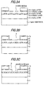
- the resist 7a is removed (FIG.3A), a resist 7b is further patterned in a shape of an aperture of a narrow recess (FIG.3B), the n-GaAs layer 4 is removed by selective etching (FIG.3C), and the narrow recess, corresponding to the second step, is formed.
- the n-AlGaAs layer 3 serves as an etching stopper layer.
- a gate electrode 10 is formed by evaporation lift-off technique on the bottom surface of the narrow recess 19, and a source electrode 11 and a drain electrode 12 are further formed on the third active layer 6 (FIG.4).
- an insulator layer 21, such as a SiN or SiO 2 layer are grown by chemical vapor deposition (CVD) method so that the insulator layer 21 covers the exposed surfaces of the active layers.
- Semiconductor of In series such as InGaAs, InGaP or InP can be used as material of a semiconductor layer.
- FIG.2A to 4 Fabrication process of a field effect transistor according to the second preferred embodiment are shown in FIG.2A to 4 also.
- An active layer 2, such as a n-GaAs layer, is grown on a GaAs substrate 1, and at a point of time that the active layer 2 becomes 100 to 250nm thick, an AlGaAs layer 3, which serves as a stopper layer in case that a narrow recess is formed, is grown till it becomes 5.0 to 30nm thick.
- a 5.0 to 100nm thick n-GaAs layer 4 is grown thereon, an about 5.0 to 30nm thick n-AlGaAs layer 5 is further grown thereon, and moreover a n-GaAs layer 6 is epitaxially grown thereon.
- a resist is patterned in a shape of an aperture of a wide recess by photolithography, and a part of the n-GaAs layer 6, which is not masked by the resist, is etched by selective etchant, such as etchant of the citric acid series.
- selective etchant such as etchant of the citric acid series.
- the stopper layer which is exposed on the surface of the wide recess, is removed by non-selective etchant of the phosphoric acid series.
- the n-AlGaAs layer can be removed independently of its thickness. The steps after that of removing the resist are the same as those of the first preferred embodiment.
- the stopper layer on the surface of the wide recess is removed, the surface state levels do not arise, so that the gate leakage current can be reduced as shown in FIG.6, and the gate breakdown voltage (Vgd) can be increased as shown in FIGs.7 and 8.
- the saturation output power Pout and the maximum power-added efficiency ⁇ add are respectively given by following equations, the high frequency characteristics (Pout, ⁇ add) are improved as shown in FIGs.9 and 10.
- the standard deviation of DC characteristic of the field effect transistors fabricated from the same wafer can be reduced as shown in FIG. 8, and the fluctuation of high frequency characteristic (RF characteristic) can be suppressed also.
- the field effect transistors with excellent and uniform characteristics can be fabricated with high reproducibility.
Landscapes
- Junction Field-Effect Transistors (AREA)
Applications Claiming Priority (3)
| Application Number | Priority Date | Filing Date | Title |
|---|---|---|---|
| JP15362197A JP3450155B2 (ja) | 1997-06-11 | 1997-06-11 | 電界効果トランジスタとその製造方法 |
| JP153621/97 | 1997-06-11 | ||
| JP15362197 | 1997-06-11 |
Publications (3)
| Publication Number | Publication Date |
|---|---|
| EP0892441A2 true EP0892441A2 (de) | 1999-01-20 |
| EP0892441A3 EP0892441A3 (de) | 1999-08-11 |
| EP0892441B1 EP0892441B1 (de) | 2008-11-26 |
Family
ID=15566501
Family Applications (1)
| Application Number | Title | Priority Date | Filing Date |
|---|---|---|---|
| EP98110701A Expired - Lifetime EP0892441B1 (de) | 1997-06-11 | 1998-06-10 | Verfahren zur Herstellung eines Feldeffekttransistors mit versenktem Gate |
Country Status (4)
| Country | Link |
|---|---|
| US (2) | US6172384B1 (de) |
| EP (1) | EP0892441B1 (de) |
| JP (1) | JP3450155B2 (de) |
| DE (1) | DE69840250D1 (de) |
Cited By (1)
| Publication number | Priority date | Publication date | Assignee | Title |
|---|---|---|---|---|
| RU2582440C1 (ru) * | 2015-02-06 | 2016-04-27 | Федеральное государственное бюджетное учреждение науки Институт сверхвысокочастотной полупроводниковой электроники Российской академии наук (ИСВЧПЭ РАН) | ПОЛУПРОВОДНИКОВАЯ ТРАНЗИСТОРНАЯ НАНОГЕТЕРОСТРУКТУРА НА ПОДЛОЖКЕ GaAs С МОДИФИЦИРОВАННЫМ СТОП-СЛОЕМ AlxGa1-xAs |
Families Citing this family (7)
| Publication number | Priority date | Publication date | Assignee | Title |
|---|---|---|---|---|
| US6528405B1 (en) * | 2000-02-18 | 2003-03-04 | Motorola, Inc. | Enhancement mode RF device and fabrication method |
| JP2005158800A (ja) * | 2003-11-20 | 2005-06-16 | Sharp Corp | 半導体装置の製造方法及びその製造方法により製造された半導体装置 |
| JP2005191022A (ja) * | 2003-12-24 | 2005-07-14 | Matsushita Electric Ind Co Ltd | 電界効果トランジスタ及びその製造方法 |
| US9768271B2 (en) * | 2013-02-22 | 2017-09-19 | Micron Technology, Inc. | Methods, devices, and systems related to forming semiconductor power devices with a handle substrate |
| US9166035B2 (en) * | 2013-09-12 | 2015-10-20 | Taiwan Semiconductor Manufacturing Company Limited | Delta doping layer in MOSFET source/drain region |
| US9536962B1 (en) | 2015-07-20 | 2017-01-03 | Taiwan Semiconductor Manufacturing Company, Ltd. | Source/drain regions for high electron mobility transistors (HEMT) and methods of forming same |
| US9583589B1 (en) | 2015-10-14 | 2017-02-28 | Northrop Grumman Systems Corporation | Self-aligned double gate recess for semiconductor field effect transistors |
Family Cites Families (16)
| Publication number | Priority date | Publication date | Assignee | Title |
|---|---|---|---|---|
| US4908325A (en) * | 1985-09-15 | 1990-03-13 | Trw Inc. | Method of making heterojunction transistors with wide band-gap stop etch layer |
| US5181087A (en) * | 1986-02-28 | 1993-01-19 | Hitachi, Ltd. | Semiconductor device and method of producing the same |
| JPS62202564A (ja) | 1986-03-03 | 1987-09-07 | Agency Of Ind Science & Technol | ヘテロ接合電界効果トランジスタ |
| JPH03160733A (ja) | 1989-11-17 | 1991-07-10 | Sanyo Electric Co Ltd | エピタキシャルウエハ |
| US5151758A (en) * | 1991-02-20 | 1992-09-29 | Comsat | Planar-doped valley field effect transistor (PDVFET) |
| US5262660A (en) * | 1991-08-01 | 1993-11-16 | Trw Inc. | High power pseudomorphic gallium arsenide high electron mobility transistors |
| JPH0582490A (ja) * | 1991-09-19 | 1993-04-02 | Hitachi Ltd | 選択エツチングの方法、装置 |
| JPH05129720A (ja) * | 1991-11-07 | 1993-05-25 | Hitachi Ltd | 半導体レーザ装置 |
| US5508535A (en) * | 1992-01-09 | 1996-04-16 | Mitsubishi Denki Kabushiki Kaisha | Compound semiconductor devices |
| JP3160733B2 (ja) | 1992-10-16 | 2001-04-25 | 大成建設株式会社 | 遮水構造物における漏水検知方法 |
| JP2581452B2 (ja) * | 1994-06-06 | 1997-02-12 | 日本電気株式会社 | 電界効果トランジスタ |
| JP2827905B2 (ja) | 1994-06-27 | 1998-11-25 | 日本電気株式会社 | Misfetおよびその製造方法 |
| JP2643849B2 (ja) * | 1994-08-01 | 1997-08-20 | 日本電気株式会社 | 半導体集積回路の製造方法 |
| JPH0897237A (ja) | 1994-09-29 | 1996-04-12 | Mitsubishi Electric Corp | 電界効果トランジスタ及びその製造方法 |
| US5739557A (en) * | 1995-02-06 | 1998-04-14 | Motorola, Inc. | Refractory gate heterostructure field effect transistor |
| JPH09321063A (ja) * | 1996-05-31 | 1997-12-12 | Nec Corp | 半導体装置およびその製造方法 |
-
1997
- 1997-06-11 JP JP15362197A patent/JP3450155B2/ja not_active Expired - Lifetime
-
1998
- 1998-06-10 EP EP98110701A patent/EP0892441B1/de not_active Expired - Lifetime
- 1998-06-10 DE DE69840250T patent/DE69840250D1/de not_active Expired - Lifetime
- 1998-06-11 US US09/095,710 patent/US6172384B1/en not_active Expired - Lifetime
-
1999
- 1999-09-01 US US09/387,500 patent/US6417035B2/en not_active Expired - Lifetime
Non-Patent Citations (2)
| Title |
|---|
| AMANO Y. ET AL: "Microwave Al0.3Ga0.7As/GaAs hetero-junction Power MISFET", TECHNICAL REPORT OF INSTITUTE OF ELECTRONICS, INFORMATION AND COMMUNICATION ENGINEERS, vol. 91, no. 218, 20 September 1991 (1991-09-20), TOKYO, JAPAN, pages 13 - 17, XP002993588 |
| TANIMOTO T. ET AL: "Double-recessed gate InGaAs channel HEMTs for low current operation", TECHNICAL REPORT OF INSTITUTE OF ELECTRONICS, INFORMATION AND COMMUNICATION ENGINEERS, vol. 91, no. 422, 20 January 1992 (1992-01-20), TOKYO, JAPAN, pages 79 - 85, XP002993589 |
Cited By (1)
| Publication number | Priority date | Publication date | Assignee | Title |
|---|---|---|---|---|
| RU2582440C1 (ru) * | 2015-02-06 | 2016-04-27 | Федеральное государственное бюджетное учреждение науки Институт сверхвысокочастотной полупроводниковой электроники Российской академии наук (ИСВЧПЭ РАН) | ПОЛУПРОВОДНИКОВАЯ ТРАНЗИСТОРНАЯ НАНОГЕТЕРОСТРУКТУРА НА ПОДЛОЖКЕ GaAs С МОДИФИЦИРОВАННЫМ СТОП-СЛОЕМ AlxGa1-xAs |
Also Published As
| Publication number | Publication date |
|---|---|
| EP0892441A3 (de) | 1999-08-11 |
| DE69840250D1 (de) | 2009-01-08 |
| EP0892441B1 (de) | 2008-11-26 |
| US6172384B1 (en) | 2001-01-09 |
| JP3450155B2 (ja) | 2003-09-22 |
| US20020016083A1 (en) | 2002-02-07 |
| JPH113896A (ja) | 1999-01-06 |
| US6417035B2 (en) | 2002-07-09 |
Similar Documents
| Publication | Publication Date | Title |
|---|---|---|
| EP0448307B1 (de) | Verfahren zur Herstellung eines leitenden Elements | |
| JP4143068B2 (ja) | 選択的エッチングした自己整列二重リセス高電子移動度トランジスターの製造方法 | |
| JP2009224801A (ja) | 増強/空乏モード擬似形態高電子移動度トランジスタデバイス | |
| JPH02148740A (ja) | 半導体装置及びその製造方法 | |
| EP0439114B1 (de) | Verfahren zur Herstellung eines Halbleiterbauelementes mit zu Source- und Drainelektrode selbstjustiertem Gate | |
| JP2891204B2 (ja) | 半導体装置の製造方法 | |
| EP1131849B1 (de) | Pseudomorphe transistoren mit hoher elektronenbeweglichkeit | |
| US6172384B1 (en) | Field effect transistor and a method for manufacturing a same | |
| US5362658A (en) | Method for producing semiconductor device | |
| JPH03194931A (ja) | 半導体装置の製造方法 | |
| EP0367411A2 (de) | Heteroübergang-Halbleiteranordnungen und Verfahren zu deren Herstellung | |
| JPH11177079A (ja) | 電界効果トランジスタ | |
| JP3903243B2 (ja) | 電界効果型半導体装置の製造方法 | |
| US6163041A (en) | Field effect transistor and method of manufacturing the same | |
| JP2914429B2 (ja) | 半導体集積回路の製造方法 | |
| JP3123445B2 (ja) | 半導体装置の製造方法 | |
| JP3903241B2 (ja) | 化合物電界効果型半導体装置 | |
| JP2000243917A (ja) | 半導体装置およびその製造方法 | |
| JP2000058560A (ja) | 電界効果トランジスタおよびその製造方法 | |
| JPH07135220A (ja) | 半導体装置およびその製造方法 | |
| JPH07202173A (ja) | 半導体装置及びその製造方法 | |
| JP2000353789A (ja) | 化合物半導体装置およびその製造方法 | |
| JP2004047621A (ja) | 半導体装置及びその製造方法 | |
| JPH0595004A (ja) | 電界効果トランジスタの製造方法 | |
| JPH05283438A (ja) | 2段リセス型fetの製造方法 |
Legal Events
| Date | Code | Title | Description |
|---|---|---|---|
| PUAI | Public reference made under article 153(3) epc to a published international application that has entered the european phase |
Free format text: ORIGINAL CODE: 0009012 |
|
| AK | Designated contracting states |
Kind code of ref document: A2 Designated state(s): DE FR GB |
|
| AX | Request for extension of the european patent |
Free format text: AL;LT;LV;MK;RO;SI |
|
| PUAL | Search report despatched |
Free format text: ORIGINAL CODE: 0009013 |
|
| AK | Designated contracting states |
Kind code of ref document: A3 Designated state(s): AT BE CH CY DE DK ES FI FR GB GR IE IT LI LU MC NL PT SE |
|
| AX | Request for extension of the european patent |
Free format text: AL;LT;LV;MK;RO;SI |
|
| 17P | Request for examination filed |
Effective date: 19990629 |
|
| AKX | Designation fees paid |
Free format text: DE FR GB |
|
| RAP1 | Party data changed (applicant data changed or rights of an application transferred) |
Owner name: NEC COMPOUND SEMICONDUCTOR DEVICES, LTD. |
|
| TPAC | Observations filed by third parties |
Free format text: ORIGINAL CODE: EPIDOSNTIPA |
|
| RAP1 | Party data changed (applicant data changed or rights of an application transferred) |
Owner name: NEC ELECTRONICS CORPORATION |
|
| 17Q | First examination report despatched |
Effective date: 20061030 |
|
| GRAP | Despatch of communication of intention to grant a patent |
Free format text: ORIGINAL CODE: EPIDOSNIGR1 |
|
| RTI1 | Title (correction) |
Free format text: METHOD FOR MANUFACTURING A FIELD EFFECT TRANSISTOR WITH RECESSED GATE |
|
| GRAS | Grant fee paid |
Free format text: ORIGINAL CODE: EPIDOSNIGR3 |
|
| GRAA | (expected) grant |
Free format text: ORIGINAL CODE: 0009210 |
|
| AK | Designated contracting states |
Kind code of ref document: B1 Designated state(s): DE FR GB |
|
| REG | Reference to a national code |
Ref country code: GB Ref legal event code: FG4D |
|
| REF | Corresponds to: |
Ref document number: 69840250 Country of ref document: DE Date of ref document: 20090108 Kind code of ref document: P |
|
| PLBE | No opposition filed within time limit |
Free format text: ORIGINAL CODE: 0009261 |
|
| STAA | Information on the status of an ep patent application or granted ep patent |
Free format text: STATUS: NO OPPOSITION FILED WITHIN TIME LIMIT |
|
| 26N | No opposition filed |
Effective date: 20090827 |
|
| PGFP | Annual fee paid to national office [announced via postgrant information from national office to epo] |
Ref country code: GB Payment date: 20090610 Year of fee payment: 12 |
|
| REG | Reference to a national code |
Ref country code: FR Ref legal event code: CD |
|
| GBPC | Gb: european patent ceased through non-payment of renewal fee |
Effective date: 20100610 |
|
| PG25 | Lapsed in a contracting state [announced via postgrant information from national office to epo] |
Ref country code: GB Free format text: LAPSE BECAUSE OF NON-PAYMENT OF DUE FEES Effective date: 20100610 |
|
| REG | Reference to a national code |
Ref country code: DE Ref legal event code: R082 Ref document number: 69840250 Country of ref document: DE Representative=s name: GLAWE DELFS MOLL - PARTNERSCHAFT VON PATENT- U, DE |
|
| REG | Reference to a national code |
Ref country code: DE Ref legal event code: R082 Ref document number: 69840250 Country of ref document: DE Representative=s name: GLAWE DELFS MOLL PARTNERSCHAFT MBB VON PATENT-, DE Effective date: 20120828 Ref country code: DE Ref legal event code: R082 Ref document number: 69840250 Country of ref document: DE Representative=s name: GLAWE DELFS MOLL - PARTNERSCHAFT VON PATENT- U, DE Effective date: 20120828 Ref country code: DE Ref legal event code: R081 Ref document number: 69840250 Country of ref document: DE Owner name: TESSERA ADVANCED TECHNOLOGIES, INC., SAN JOSE, US Free format text: FORMER OWNER: NEC ELECTRONICS CORP., KAWASAKI, KANAGAWA, JP Effective date: 20120828 Ref country code: DE Ref legal event code: R081 Ref document number: 69840250 Country of ref document: DE Owner name: RENESAS ELECTRONICS CORPORATION, JP Free format text: FORMER OWNER: NEC ELECTRONICS CORP., KAWASAKI, JP Effective date: 20120828 |
|
| REG | Reference to a national code |
Ref country code: DE Ref legal event code: R082 Ref document number: 69840250 Country of ref document: DE Representative=s name: GLAWE DELFS MOLL PARTNERSCHAFT MBB VON PATENT-, DE |
|
| REG | Reference to a national code |
Ref country code: DE Ref legal event code: R082 Ref document number: 69840250 Country of ref document: DE Representative=s name: GLAWE DELFS MOLL PARTNERSCHAFT MBB VON PATENT-, DE Effective date: 20140829 Ref country code: DE Ref legal event code: R081 Ref document number: 69840250 Country of ref document: DE Owner name: TESSERA ADVANCED TECHNOLOGIES, INC., SAN JOSE, US Free format text: FORMER OWNER: RENESAS ELECTRONICS CORPORATION, KAWASAKI-SHI, KANAGAWA, JP Effective date: 20140829 |
|
| REG | Reference to a national code |
Ref country code: FR Ref legal event code: TP Owner name: TESSERA ADVANCED TECHNOLOGIES, INC., US Effective date: 20141013 |
|
| REG | Reference to a national code |
Ref country code: FR Ref legal event code: PLFP Year of fee payment: 19 |
|
| REG | Reference to a national code |
Ref country code: FR Ref legal event code: PLFP Year of fee payment: 20 |
|
| PGFP | Annual fee paid to national office [announced via postgrant information from national office to epo] |
Ref country code: FR Payment date: 20170627 Year of fee payment: 20 |
|
| PGFP | Annual fee paid to national office [announced via postgrant information from national office to epo] |
Ref country code: DE Payment date: 20170628 Year of fee payment: 20 |
|
| REG | Reference to a national code |
Ref country code: DE Ref legal event code: R071 Ref document number: 69840250 Country of ref document: DE |