EP0905785A2 - Mémoire semi-conductrice à haute densité - Google Patents
Mémoire semi-conductrice à haute densité Download PDFInfo
- Publication number
- EP0905785A2 EP0905785A2 EP98307876A EP98307876A EP0905785A2 EP 0905785 A2 EP0905785 A2 EP 0905785A2 EP 98307876 A EP98307876 A EP 98307876A EP 98307876 A EP98307876 A EP 98307876A EP 0905785 A2 EP0905785 A2 EP 0905785A2
- Authority
- EP
- European Patent Office
- Prior art keywords
- memory
- lines
- bit line
- word line
- word lines
- Prior art date
- Legal status (The legal status is an assumption and is not a legal conclusion. Google has not performed a legal analysis and makes no representation as to the accuracy of the status listed.)
- Ceased
Links
- 239000004065 semiconductor Substances 0.000 title claims abstract description 23
- 230000015654 memory Effects 0.000 claims abstract description 112
- 230000009977 dual effect Effects 0.000 claims abstract description 24
- 230000000295 complement effect Effects 0.000 claims description 32
- 239000003990 capacitor Substances 0.000 description 4
- 239000000872 buffer Substances 0.000 description 3
- VYPSYNLAJGMNEJ-UHFFFAOYSA-N Silicium dioxide Chemical compound O=[Si]=O VYPSYNLAJGMNEJ-UHFFFAOYSA-N 0.000 description 2
- 229910052782 aluminium Inorganic materials 0.000 description 2
- XAGFODPZIPBFFR-UHFFFAOYSA-N aluminium Chemical compound [Al] XAGFODPZIPBFFR-UHFFFAOYSA-N 0.000 description 2
- 238000003491 array Methods 0.000 description 2
- 230000001419 dependent effect Effects 0.000 description 2
- 238000010586 diagram Methods 0.000 description 2
- 238000005516 engineering process Methods 0.000 description 2
- 230000001788 irregular Effects 0.000 description 2
- 230000001413 cellular effect Effects 0.000 description 1
- 239000004020 conductor Substances 0.000 description 1
- 230000000694 effects Effects 0.000 description 1
- 230000006870 function Effects 0.000 description 1
- 229910052751 metal Inorganic materials 0.000 description 1
- 239000002184 metal Substances 0.000 description 1
- 238000001465 metallisation Methods 0.000 description 1
- 230000000737 periodic effect Effects 0.000 description 1
- 229910021420 polycrystalline silicon Inorganic materials 0.000 description 1
- 229920005591 polysilicon Polymers 0.000 description 1
- 229910021332 silicide Inorganic materials 0.000 description 1
- FVBUAEGBCNSCDD-UHFFFAOYSA-N silicide(4-) Chemical compound [Si-4] FVBUAEGBCNSCDD-UHFFFAOYSA-N 0.000 description 1
- 235000012239 silicon dioxide Nutrition 0.000 description 1
- 239000000377 silicon dioxide Substances 0.000 description 1
- 239000007787 solid Substances 0.000 description 1
Images


Classifications
-
- G—PHYSICS
- G11—INFORMATION STORAGE
- G11C—STATIC STORES
- G11C7/00—Arrangements for writing information into, or reading information out from, a digital store
- G11C7/18—Bit line organisation; Bit line lay-out
-
- G—PHYSICS
- G11—INFORMATION STORAGE
- G11C—STATIC STORES
- G11C11/00—Digital stores characterised by the use of particular electric or magnetic storage elements; Storage elements therefor
- G11C11/21—Digital stores characterised by the use of particular electric or magnetic storage elements; Storage elements therefor using electric elements
- G11C11/34—Digital stores characterised by the use of particular electric or magnetic storage elements; Storage elements therefor using electric elements using semiconductor devices
- G11C11/40—Digital stores characterised by the use of particular electric or magnetic storage elements; Storage elements therefor using electric elements using semiconductor devices using transistors
- G11C11/401—Digital stores characterised by the use of particular electric or magnetic storage elements; Storage elements therefor using electric elements using semiconductor devices using transistors forming cells needing refreshing or charge regeneration, i.e. dynamic cells
- G11C11/4063—Auxiliary circuits, e.g. for addressing, decoding, driving, writing, sensing or timing
- G11C11/407—Auxiliary circuits, e.g. for addressing, decoding, driving, writing, sensing or timing for memory cells of the field-effect type
- G11C11/409—Read-write [R-W] circuits
- G11C11/4097—Bit-line organisation, e.g. bit-line layout, folded bit lines
-
- G—PHYSICS
- G11—INFORMATION STORAGE
- G11C—STATIC STORES
- G11C8/00—Arrangements for selecting an address in a digital store
- G11C8/14—Word line organisation; Word line lay-out
-
- H—ELECTRICITY
- H10—SEMICONDUCTOR DEVICES; ELECTRIC SOLID-STATE DEVICES NOT OTHERWISE PROVIDED FOR
- H10B—ELECTRONIC MEMORY DEVICES
- H10B12/00—Dynamic random access memory [DRAM] devices
- H10B12/30—DRAM devices comprising one-transistor - one-capacitor [1T-1C] memory cells
- H10B12/48—Data lines or contacts therefor
- H10B12/482—Bit lines
-
- H—ELECTRICITY
- H10—SEMICONDUCTOR DEVICES; ELECTRIC SOLID-STATE DEVICES NOT OTHERWISE PROVIDED FOR
- H10B—ELECTRONIC MEMORY DEVICES
- H10B12/00—Dynamic random access memory [DRAM] devices
- H10B12/30—DRAM devices comprising one-transistor - one-capacitor [1T-1C] memory cells
- H10B12/48—Data lines or contacts therefor
- H10B12/488—Word lines
-
- H—ELECTRICITY
- H10—SEMICONDUCTOR DEVICES; ELECTRIC SOLID-STATE DEVICES NOT OTHERWISE PROVIDED FOR
- H10B—ELECTRONIC MEMORY DEVICES
- H10B12/00—Dynamic random access memory [DRAM] devices
- H10B12/01—Manufacture or treatment
- H10B12/02—Manufacture or treatment for one transistor one-capacitor [1T-1C] memory cells
- H10B12/03—Making the capacitor or connections thereto
- H10B12/038—Making the capacitor or connections thereto the capacitor being in a trench in the substrate
Definitions
- This invention relates generally to semiconductor memories such as dynamic random access memories (DRAMs). More specifically, this invention relates to a space efficient architecture for a high density semiconductor memory having diagonal bit lines to facilitate memory cell access, and having dual word lines on different, vertically-spaced layers.
- DRAMs dynamic random access memories
- Each memory cell is comprised of an access transistor (e.g., an NFET) and a capacitor such as a trench capacitor for storing charge corresponding to a data bit.
- the memory cells are typically located at the intersections of the word lines and bit lines.
- the gate electrode of each access transistor is electrically connected to the associated word line while the transistor's drain terminal is connected to the associated bit line.
- true memory cells are located in close proximity to corresponding complementary memory cells.
- the true cells are connected to true bit lines and the complementary cells are connected to complementary bit lines.
- a true bit line and an adjacent complementary bit line form a bit line pair.
- the bit line pair is typically connected at one end to a sense amplifier.
- column is sometimes used herein to refer to a bit line pair.
- the true and complementary bit lines Prior to reading data from a true cell, the true and complementary bit lines are precharged with a certain precharge voltage, and then left floating at that voltage.
- the access transistor is switched on, thereby modifying the voltage level on the true bit line due to charge sharing with the memory cell capacitor.
- the voltage on the complementary bit line remains at the precharge voltage, whereby a differential voltage is applied to the sense amplifier.
- the sense amplifier then amplifies the differential voltage to provide a solid logic level for readout and restore operations.
- the true bit line is held at the precharge voltage while the word line coupled to the complementary cell is raised, whereby an analogous differential voltage is amplified by the sense amplifier.
- a word line configuration designed to reduce memory cell access time (RC time constant of the word line) is referred to herein as a dual word line configuration.
- a dual word line consists of a master word line running continuously across the entire memory cell array or subarray, and a number of local word lines, either connected to or separated from each other, each electrically connecting a predetermined number of memory cells in an associated row to one master word line.
- One master word line and multiple local word lines are used for each row of the array.
- Each master word line overlies the associated local word lines on a different vertically-spaced layer, with a suitable dielectric layer separating the two layers.
- the master word line is composed of a low resistivity metal such as aluminum whereas the local word lines are typically composed of highly doped polysilicon with a silicide layer on top.
- the local word lines are electrically connected to the associated master word line by means of periodic electrical via hole contacts (stitches) between the layers.
- word line drivers employing FET switches are used in place of the via hole contacts. With either approach, the total resistance in the path to any given memory cell is substantially reduced. With lower word line resistance, the RC time constant associated with each word line is reduced, thereby reducing memory cell access time.
- the segmented architecture has the additional advantage of reduced word line capacitance; however, a drawback to this configuration is the additional complexity and space required for the local word line drivers.
- DBL diagonal bit line
- F the minimum feature size of the processing technology.
- An example of a diagonal bit line type DRAM is disclosed in an article entitled “FA 14.6: A 1Gb DRAM for File Applications", by T. Sugibayashi et al., ISSC95/Session 14. That article discloses a DRAM using an open bit line architecture.
- the open bit line architecture is more susceptible to noise-related problems than a folded bit line architecture.
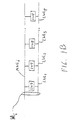
- each memory array in the DRAM is divided into multiple memory blocks such as B1, B2 and B3.
- Dual word lines such as WL i or WL y extend across multiple blocks and are driven by a main word line driver 93.
- Local word line drivers are disposed in areas L D between the blocks.
- each dual word line as WL i consists of a master word line MWL i and a number P of local word lines LWL 1 -LWL P .
- a local word line driver LWD is coupled between each local word line and the master word line.
- Each local word line driver operates to drive the associated local word line to permit selective access to the cells coupled to that local word line.
- Folded bit line pairs such as BLP j , BLP i , BLP y are each coupled to a respective sense amplifier within sense amplifier bank 92.
- Each pair as BLP j consists of a true bit line BL j and a complementary bit line BL j .
- the bit lines run diagonally with respect to the word lines, changing direction at twist regions 33. Direction changes occur every K word lines, where K is typically 2 N , e.g., eight, sixteen, thirty-two, sixty-four, etc.
- the true and complementary bit lines of each bit line pair are vertically spaced from one another, alternatingly overlying and underlying one another.
- a three dimensional twist occurs such that the vertical positions of the true and complementary bitlines change with respect to one another.
- This three dimensional twist will be referred to herein as a vertical twist.
- a change in horizontal direction can also occur.
- the bit lines define zigzag-type patterns in the horizontal plane along the memory array.
- the zigzag patterns of the bit lines in conjunction with the locations of the local word line drivers between memory blocks, results in wasted chip area in the regions Ap at the edge of each memory block.
- the area penalty is a function of the bit line slant angle ⁇ of the pattern and the length D T of the vertical twist regions.
- the invention also relates to a DRAM or to an IC chip incorporating the semiconductor memory in accordance with the invention.
- the present invention is directed towards a high density semiconductor memory having diagonal bit lines and a dual word line configuration with highly efficient use of chip area.
- the semiconductor memory includes a memory cell array of memory cells arranged in rows and columns, and a plurality of diagonal bit lines arranged in a pattern that changes horizontal direction along the memory cell array to facilitate access to the memory cells.
- the bit lines are arranged non-orthogonal to a plurality of dual word lines, where each dual word line includes a master word line at a first layer and a plurality of local word lines at a second layer.
- the local word lines each connect to plural memory cells and to the master word line of a common row via a plurality of spaced electrical connections.
- the electrical connections which may be, e.g., electrical contacts, run in substantially the same pattern in the horizontal plane along the memory cell array as the bit lines.
- the bit lines may be arranged in folded or open configurations.
- the substantial area penalty exhibited by prior art diagonal bit line type memories of the segmented word line type is largely eliminated with the present invention.
- the present invention relates to a space-efficient, high density semiconductor memory employing diagonal bit lines and dual word lines with a space efficient architecture.
- the invention provides a way to substantially eliminate the area penalty associated with diagonal bit line type memories.
- an exemplary embodiment of the invention is described in the context of a DRAM chip. The invention however has broader applications.
- the invention has application in other memory devices such as EDO-DRAM, SDRAM, RAMBUS-DRAM, MDRAM, SRAM, flash RAM, EPROM, EEPROM, or mask ROM, or merged DRAM-logic (embedded DRAM).
- the devices are used in, for example, consumer products such as computer systems, cellular phones, personal digital assistants (PDAs), and other electronic products.
- a memory cell array 12 of DRAM 10 comprises of memory cells MC arranged in an array of M rows by N columns.
- M and N may each be on the order of several thousand or tens of thousands.
- Each one of M dual word lines WL 1 to WL M is electrically coupled to memory cells MC of an associated row such as R j .
- FIG. 11 schematically illustrates one of the dual word lines WL j in the vertical plane (where the major surface of the memory cell array is defined as being in the horizontal plane).
- Dual word line WL j consists of a master word line MWLj and X local word lines LWL 1 -LWL X oriented along the associated row.
- the master word lines and local word lines are fabricated on different, vertically spaced layers, and each master word line overlies the associated local word lines in the respective row.
- Each local word line is electrically connected to the associated master word line by an electrical contact (stitch) 29.
- This type of arrangement is known as a stitched dual word line architecture, mentioned above.
- the local word lines LWL 1 -LWL X of any given row are preferably formed as a continuous line along the array, but may alternatively be separated by spacings S as shown.
- incoming addresses to DRAM 10 are applied to an address buffer 11 which in turn provides the addresses to a row decoder 13 and a column decoder 15 as is conventional.
- Row decoder 13 operates in conjunction with a word line driver 19 to activate the master word line corresponding to the row of the incoming address.
- column decoder 15 activates one of column select lines CSL 1 to CSLy corresponding to the column of the incoming address, whereby data can be written into or read from the particular memory cell corresponding to the row and column of the address.
- a sense amplifier bank 21 includes N sense amplifiers SA 1 -SA N , one for each column, each of which is coupled to a corresponding bit line pair BLP 1 -BLP N .
- a master data line 22 connects to each sense amplifier in the bank and carries data to or from the target memory cell at any given time.
- Input/output (I/O) buffer 23 connects to data line 22, and buffers incoming and outgoing data in a conventional manner.
- bit lines employed in the present invention are diagonal bit lines conducive to accessing small memory cells such as 6F 2 cells.
- the memory cells may be conventional diagonal bit line cells similar to those disclosed in the T. Sugibayashi et al. article cited hereinabove.
- the bit lines are shown as folded bit lines, where a bit line pair, such as BLP j , comprises true and complementary diagonal bit lines BL j , BL j as was the case for the bit lines of FIGS. 1A and 2 described above.
- a bit line pair such as BLP j
- the present invention is applicable to both a folded bit line architecture and to an open bit line architecture.
- the open line architecture will be discussed further below.
- each bit line pair as BLPj may be the same as that shown in FIG. 2.
- Each pair comprises of a true bit line BL j electrically connected to the true memory cells MC in column Cj, and a complementary bit line BL j connected to the complementary cells in column C j .
- the true and complementary bit lines are aligned with one another in the vertical plane (where the major surface of the memory cell array is in the horizontal plane).
- the true bit lines are periodically twisted at locations 33 in the vertical plane with the associated complementary bit lines as was discussed earlier.
- the true bit line alternately overlies and underlies the associated complementary bit line, where the two lines are vertically spaced by a dielectric layer. That is, alternating portions of the true bit line run on top of the complementary bit line, and vice versa.
- the twists occur after every K word lines, where K is preferably 2 N , e.g., eight, sixteen, thirty-two sixty-four, etc.
- each bit line pair runs in a zigzag-type pattern as was described above in reference to FIG. 1A.
- the slanted direction (i.e., slanted with respect to the word lines) of the zigzag pattern changes at every twist of the true and complementary bit lines, i.e. at locations 33.
- the electrical contacts or stitches 29 that connect the local word lines to the associated master word line follow the same zigzag pattern in the horizontal plane as the bit lines. Accordingly, the above-described area penalty of the segmented architecture of FIG. 1A is largely eliminated. That is, unused area "Ap" of FIG. 1A is substantially reduced to zero.
- the only additional area of the memory cell array which is required to implement the stitched architecture of the present invention is the area occupied by the stitches themselves, e.g., three microns per stitch (including the area of dummy bit lines on both sides of each stitch 29 as necessary).
- the memory cell area in between each zigzag pattern of stitches 29 defines a memory cell block such as Bq, analogous to the memory blocks B1-B3 of FIG. 1A.
- Adjacent memory cell blocks such as Bq and Bq+1 "fit" together in a space efficient manner.
- the stitches 29 of adjacent local word lines as LWL y , LWL y+1 are separated by a distance D, where D is dependent on the number of memory cells allocated to each local word line, and the dimensions of each memory cell.
- D is dependent on the number of memory cells allocated to each local word line, and the dimensions of each memory cell.
- the regions where changes in horizontal direction of the bit lines occur are not coincident with the vertical twist regions of the bit lines.
- the changes in horizontal direction would occur at the regions 33 as shown in FIG. 4, but the vertical twists would occur somewhere in between the shown regions 33.
- the distance D between adjacent local word lines may be different for different portions of each row. For example, it is preferable to allocate a lower number of memory cells to the local word lines further away from the word line driver than for those closer to the word line driver, whereby the distance D becomes progressively smaller as the row extends away from the word line driver.
- This approach is illustrated in FIG. 5.
- the distance D1 between the stitch 29 of the first local word line LWL 1 to the stitch 29 of LWL 2 is substantially greater than the distance DX between the next to last local word line LWL X-1 and the last local word line LWL X of each row. It is noted that each stitch 29 preferably connects the master word line to the center of each associated local word line.
- 5 allows for a reduction in the total number of stitches in each row, since, as compared to the case in which uniform local word line spacings are used, a larger number of memory cells can be allocated to the local word lines closer to the word line driver.
- the irregular spacing approach is feasible because the limiting factor in the local word line lengths is the delay time from the word line driver to the last memory cell of each local word line. If uniform spacings are used, the delay times are shorter for the memory cells closest to the word line driver, whereas if irregular spacings are used, the delay times of all cells may be approximately equalized.
- the local word lines may be separated from one another by a distance S as shown.
- all the local word lines may be formed as one continuous, electrically conductive line, whereby S is zero.
- the latter approach is taken, with the local word lines being formed integrally with the gate electrodes of all the memory cells (true or complementary) in the row.
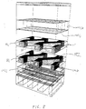
- FIG. 6 there is shown a plan view of a portion of the memory cell array 12 corresponding to approximately two memory cell areas.
- FIG. 7 is the cross-sectional view taken along the lines 7-7 of FIG. 6.
- a true bit line as BL j directly overlies a complementary bit line BL i .
- the complementary bit line overlies the true bit line.
- the bit lines are separated by a dielectric layer 44 such as silicon dioxide.
- a typical thickness for layer 44 is about 400 nanometers and an exemplary width for each bit line is about the minimum feature size F, e.g., 0.25 um (for .25 micron technology).
- each bit line is comprised of portions 25 which are orthogonal to the word lines such as MWL j , MWL j+1 , and portions 28 that are slanted with respect to the word lines.
- portions 25 which are orthogonal to the word lines such as MWL j , MWL j+1 , and portions 28 that are slanted with respect to the word lines.
- An exemplary angle ⁇ 1 of portion 28 with respect to the word lines is about 45°.
- the portions 25 orthogonal to the word lines can be eliminated, whereby the bit lines run diagonally in a continuous fashion for each segment of K word lines.
- Electrical contacts or stitches 29 are shown adjacent bit line BL i and extend, as shown in FIG. 7, from the master word line as MWLj to the associated local word line LWL j , the latter of which is preferably integrated with the gate conductors of the transistors in the row.
- the master word line as MWL j is separated from the top bit lines by another dielectric layer 42.
- a dielectric layer 46 separates the lower bit lines from the local word lines.
- interconnects 34 for interconnecting bit lines to the drains of the associated memory cell transistors, and trench capacitor regions 36 and 38 of respective memory cells. Suitable metallization such as aluminum, is used to form the stitches 29.
- the diameter of stitches 29 is approximately the width of a bitline, e.g., .25um.
- the area that needs to be allocated for the stitch region is larger, e.g. 1-5 um, because one or two dummy bit lines on both sides of each stitch are typically necessary.
- the area occupied by the dummy bit lines is significantly larger than the stitch itself.
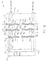
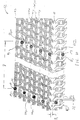
- FIG. 8 a perspective view of a three dimensional section of memory array 12 is shown.
- the section corresponds to approximately three memory cells of the array.
- the reference numerals depicted in FIG. 8 correspond to those in FIGS. 6 and 7.
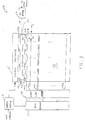
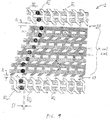
- FIG. 9 there is shown a plan view of a portion of an exemplary layout of memory cell array 12 showing only bit lines, word lines and stitches 29.
- the bit line pairs are vertically twisted to facilitate access to the memory cells.
- the true bit lines as BLi run on top of complementary bit lines and the complementary bit lines access the memory cells in that portion.
- K is preferably 2 N , e.g., eight, sixteen, thirty-two, sixty-four, etc.
- a vertical twist occurs at the lower and upper junctures 33, whereby the complementary bit lines such as BL i then run on top of the true bit lines as BLi.
- the complementary bit lines overlie the true bit lines, and the true bit lines access the true memory cells for K consecutive word lines.
- the configuration of the vertical twist regions 33 may be similar to or essentially the same as that disclosed in the DeBrosse et al. patent application mentioned above.
- the horizontal distance D T of each vertical twist region 33 is typically on the order of three microns.
- the slant angle ⁇ 2 between the dotted line 36 and the direction of the word lines is generally the slant angle of the overall zigzag pattern.
- a typical slant angle ⁇ 2 is on the order of 65°.
- the electrical contacts 29 are laid out in generally the same zigzag pattern as the bit lines. In the embodiment of FIG. 9, each contact 29 is spaced at approximately the same distance S1 from the adjacent bit line in the row.
- the bit lines on both sides of each stitch 29, such as BL j and BL j-1 are actually dummy bit lines as discussed above.
- the above-described exemplary layout of FIG. 9 is shown over a larger number of columns.
- the stitches 29 are arranged in an interleaved configuration such that the local word lines such as LWL y-1 and LWL y are in a row to row staggered configuration.
- the distance D between adjacent contacts 29 of a common row is dependent upon the number of memory cells allocated to the local word line.
- DRAM 10 is typically a multi-array DRAM having several subarrays of memory cells. Each subarray may be essentially identical to the above-described array 12, with folded bit lines running in a zigzag pattern, with the electrical contacts 29 generally following the pattern of the bit lines, and generally following the pattern of the bit lines, and so forth.
- FIG. 4 may be envisioned as one half of an open bit line architecture, with the bit lines designated such as BLP i representing a single bit line rather than a bit line pair.
- BLP i the bit lines designated such as BLP i representing a single bit line rather than a bit line pair.
- the other side of the open bit line architecture would reside atop the sense amplifier bank 21 of FIG. 4.
- the layout of the open bit line architecture would correspond to that of FIGS. 9 or 10, except that at regions 33, there would be no vertical twists -- the bit lines would only undergo a change in horizontal direction.
- the plan view would represent only the singular bit lines of the open bit line configuration rather than alternating true and complementary bit lines.
- sense amplifiers of the folded bit line configurations described above have been shown in unshared configurations, it is understood that they may be in shared configurations with memory cell arrays on either side, and with bit line pairs coupled to the sense amplifiers on either side.
- the shared configuration is advantageous in terms of space efficiency, since less space consuming sense amplifiers are employed for a given memory capacity.
Landscapes
- Engineering & Computer Science (AREA)
- Microelectronics & Electronic Packaging (AREA)
- Computer Hardware Design (AREA)
- Semiconductor Memories (AREA)
- Dram (AREA)
- Static Random-Access Memory (AREA)
Applications Claiming Priority (2)
| Application Number | Priority Date | Filing Date | Title |
|---|---|---|---|
| US08/939,455 US5864496A (en) | 1997-09-29 | 1997-09-29 | High density semiconductor memory having diagonal bit lines and dual word lines |
| US939455 | 1997-09-29 |
Publications (2)
| Publication Number | Publication Date |
|---|---|
| EP0905785A2 true EP0905785A2 (fr) | 1999-03-31 |
| EP0905785A3 EP0905785A3 (fr) | 2003-08-13 |
Family
ID=25473216
Family Applications (1)
| Application Number | Title | Priority Date | Filing Date |
|---|---|---|---|
| EP98307876A Ceased EP0905785A3 (fr) | 1997-09-29 | 1998-09-29 | Mémoire semi-conductrice à haute densité |
Country Status (6)
| Country | Link |
|---|---|
| US (1) | US5864496A (fr) |
| EP (1) | EP0905785A3 (fr) |
| JP (1) | JPH11163299A (fr) |
| KR (1) | KR100564662B1 (fr) |
| CN (1) | CN1244932C (fr) |
| TW (1) | TW439063B (fr) |
Cited By (3)
| Publication number | Priority date | Publication date | Assignee | Title |
|---|---|---|---|---|
| WO2004109705A3 (fr) * | 2003-06-09 | 2005-03-03 | Toshiba Kk | Memoire ferroelectrique |
| US7092274B2 (en) | 2003-06-16 | 2006-08-15 | Kabushiki Kaisha Toshiba | Ferroelectric memory device |
| JP2013145875A (ja) * | 2011-12-15 | 2013-07-25 | Semiconductor Energy Lab Co Ltd | 記憶装置 |
Families Citing this family (51)
| Publication number | Priority date | Publication date | Assignee | Title |
|---|---|---|---|---|
| JP3110348B2 (ja) * | 1997-06-18 | 2000-11-20 | 日本電気アイシーマイコンシステム株式会社 | 半導体記憶装置 |
| US6025221A (en) * | 1997-08-22 | 2000-02-15 | Micron Technology, Inc. | Processing methods of forming integrated circuitry memory devices, methods of forming DRAM arrays, and related semiconductor masks |
| US6191443B1 (en) | 1998-02-28 | 2001-02-20 | Micron Technology, Inc. | Capacitors, methods of forming capacitors, and DRAM memory cells |
| US6730559B2 (en) | 1998-04-10 | 2004-05-04 | Micron Technology, Inc. | Capacitors and methods of forming capacitors |
| US6333866B1 (en) * | 1998-09-28 | 2001-12-25 | Texas Instruments Incorporated | Semiconductor device array having dense memory cell array and heirarchical bit line scheme |
| US7031214B2 (en) * | 1999-01-14 | 2006-04-18 | Silicon Storage Technology, Inc. | Digital multilevel memory system having multistage autozero sensing |
| DE19903197A1 (de) * | 1999-01-27 | 2000-03-09 | Siemens Ag | Integrierter Speicher mit segmentierter Wortleitung |
| DE19907176A1 (de) * | 1999-02-19 | 2000-08-31 | Siemens Ag | Decoder-Anschlußanordnung für Speicherchips mit langen Bitleitungen |
| JP3580719B2 (ja) * | 1999-03-03 | 2004-10-27 | 株式会社東芝 | 半導体記憶装置及びその製造方法 |
| KR100361863B1 (ko) | 1999-06-29 | 2002-11-22 | 주식회사 하이닉스반도체 | 반도체 메모리 장치 |
| US6469947B2 (en) | 1999-06-29 | 2002-10-22 | Hyundai Electronics Co., Ltd. | Semiconductor memory device having regions with independent word lines alternately selected for refresh operation |
| US6320780B1 (en) * | 1999-09-28 | 2001-11-20 | Infineon Technologies North America Corp. | Reduced impact from coupling noise in diagonal bitline architectures |
| US6282113B1 (en) * | 1999-09-29 | 2001-08-28 | International Business Machines Corporation | Four F-squared gapless dual layer bitline DRAM array architecture |
| US6504246B2 (en) * | 1999-10-12 | 2003-01-07 | Motorola, Inc. | Integrated circuit having a balanced twist for differential signal lines |
| US7005695B1 (en) * | 2000-02-23 | 2006-02-28 | Micron Technology, Inc. | Integrated circuitry including a capacitor with an amorphous and a crystalline high K capacitor dielectric region |
| US7184290B1 (en) * | 2000-06-28 | 2007-02-27 | Marvell International Ltd. | Logic process DRAM |
| US6496402B1 (en) * | 2000-10-17 | 2002-12-17 | Intel Corporation | Noise suppression for open bit line DRAM architectures |
| US6912696B2 (en) * | 2000-12-05 | 2005-06-28 | Oki Electric Industry Co., Ltd. | Smart card and circuitry layout thereof for reducing cross-talk |
| CA2340985A1 (fr) | 2001-03-14 | 2002-09-14 | Atmos Corporation | Architecture canal mot entrelacee |
| JP3910047B2 (ja) * | 2001-11-20 | 2007-04-25 | 松下電器産業株式会社 | 半導体記憶装置 |
| US20030235089A1 (en) * | 2002-04-02 | 2003-12-25 | Gerhard Mueller | Memory array with diagonal bitlines |
| TW536789B (en) * | 2002-04-18 | 2003-06-11 | Macronix Int Co Ltd | Mask ROM |
| US7042749B2 (en) * | 2002-05-16 | 2006-05-09 | Micron Technology, Inc. | Stacked 1T-nmemory cell structure |
| KR100456598B1 (ko) * | 2002-09-09 | 2004-11-09 | 삼성전자주식회사 | 서로 상보되는 데이터를 갖는 메모리 셀들이 배열되는메모리 장치 |
| US6657880B1 (en) | 2002-12-04 | 2003-12-02 | Virtual Silicon Technology, Inc. | SRAM bit line architecture |
| US7371627B1 (en) * | 2005-05-13 | 2008-05-13 | Micron Technology, Inc. | Memory array with ultra-thin etched pillar surround gate access transistors and buried data/bit lines |
| US7120046B1 (en) * | 2005-05-13 | 2006-10-10 | Micron Technology, Inc. | Memory array with surrounding gate access transistors and capacitors with global and staggered local bit lines |
| KR100709431B1 (ko) * | 2005-05-31 | 2007-04-18 | 주식회사 하이닉스반도체 | 6f2 셀 구조를 포함하는 반도체 소자 |
| US7888721B2 (en) * | 2005-07-06 | 2011-02-15 | Micron Technology, Inc. | Surround gate access transistors with grown ultra-thin bodies |
| US7768051B2 (en) * | 2005-07-25 | 2010-08-03 | Micron Technology, Inc. | DRAM including a vertical surround gate transistor |
| US7696567B2 (en) * | 2005-08-31 | 2010-04-13 | Micron Technology, Inc | Semiconductor memory device |
| US7616492B2 (en) * | 2005-10-04 | 2009-11-10 | Qimonda Ag | Evaluation circuit and evaluation method for the assessment of memory cell states |
| US8872247B2 (en) | 2009-11-04 | 2014-10-28 | Micron Technology, Inc. | Memory cells having a folded digit line architecture |
| US8745555B2 (en) * | 2010-05-12 | 2014-06-03 | D2S, Inc. | Method for integrated circuit design and manufacture using diagonal minimum-width patterns |
| US8923050B2 (en) * | 2012-06-15 | 2014-12-30 | Sandisk 3D Llc | 3D memory with vertical bit lines and staircase word lines and vertical switches and methods thereof |
| US9257152B2 (en) | 2012-11-09 | 2016-02-09 | Globalfoundries Inc. | Memory architectures having wiring structures that enable different access patterns in multiple dimensions |
| US9383411B2 (en) * | 2013-06-26 | 2016-07-05 | International Business Machines Corporation | Three-dimensional processing system having at least one layer with circuitry dedicated to scan testing and system state checkpointing of other system layers |
| US9389876B2 (en) | 2013-10-24 | 2016-07-12 | International Business Machines Corporation | Three-dimensional processing system having independent calibration and statistical collection layer |
| US9524920B2 (en) | 2013-11-12 | 2016-12-20 | Taiwan Semiconductor Manufacturing Co., Ltd. | Apparatus and method of three dimensional conductive lines |
| CN105448927B (zh) * | 2014-09-26 | 2018-07-06 | 旺宏电子股份有限公司 | 三维半导体元件 |
| US9691695B2 (en) * | 2015-08-31 | 2017-06-27 | Taiwan Semiconductor Manufacturing Company, Ltd. | Monolithic 3D integration inter-tier vias insertion scheme and associated layout structure |
| KR20170027493A (ko) * | 2015-09-02 | 2017-03-10 | 에스케이하이닉스 주식회사 | 반도체 장치의 레이아웃 구조 |
| KR102633031B1 (ko) * | 2016-11-04 | 2024-02-05 | 에스케이하이닉스 주식회사 | 반도체 메모리 소자 |
| KR102342853B1 (ko) * | 2017-07-21 | 2021-12-23 | 삼성전자주식회사 | 수직형 메모리 소자를 구비한 집적회로 소자 |
| US10818729B2 (en) * | 2018-05-17 | 2020-10-27 | Macronix International Co., Ltd. | Bit cost scalable 3D phase change cross-point memory |
| US10726922B2 (en) | 2018-06-05 | 2020-07-28 | Sandisk Technologies Llc | Memory device with connected word lines for fast programming |
| CN112885832B (zh) * | 2019-11-29 | 2024-07-16 | 长鑫存储技术有限公司 | 半导体结构及其制造方法 |
| KR102810859B1 (ko) | 2020-09-16 | 2025-05-20 | 삼성전자주식회사 | 로우 디코더를 포함하는 메모리 장치 |
| CN112366203B (zh) * | 2020-10-23 | 2023-01-03 | 福建省晋华集成电路有限公司 | 图案布局以及其形成方法 |
| US20240028880A1 (en) * | 2020-12-11 | 2024-01-25 | National University Of Singapore | Planar-staggered array for dcnn accelerators |
| CN116741227B (zh) * | 2023-08-09 | 2023-11-17 | 浙江力积存储科技有限公司 | 一种三维存储器架构及其操作方法和存储器 |
Citations (1)
| Publication number | Priority date | Publication date | Assignee | Title |
|---|---|---|---|---|
| JPH09135004A (ja) * | 1995-11-10 | 1997-05-20 | Nec Corp | 半導体記憶装置 |
Family Cites Families (24)
| Publication number | Priority date | Publication date | Assignee | Title |
|---|---|---|---|---|
| JPS60206164A (ja) * | 1984-03-30 | 1985-10-17 | Toshiba Corp | 半導体メモリ装置 |
| JPS62188261A (ja) * | 1986-01-16 | 1987-08-17 | Sony Corp | メモリ装置 |
| US5214601A (en) * | 1986-12-11 | 1993-05-25 | Mitsubishi Denki Kabushiki Kaisha | Bit line structure for semiconductor memory device including cross-points and multiple interconnect layers |
| JP2681285B2 (ja) * | 1988-09-19 | 1997-11-26 | 富士通株式会社 | 半導体記憶装置 |
| JPH02288362A (ja) * | 1989-04-28 | 1990-11-28 | Sony Corp | 半導体メモリ |
| US5194752A (en) * | 1989-05-23 | 1993-03-16 | Kabushiki Kaisha Toshiba | Semiconductor memory device |
| JPH07114258B2 (ja) * | 1989-09-13 | 1995-12-06 | 東芝マイクロエレクトロニクス株式会社 | 半導体メモリ |
| JPH03105969A (ja) * | 1989-09-19 | 1991-05-02 | Fujitsu Ltd | 半導体記憶装置 |
| JPH03278573A (ja) * | 1990-03-28 | 1991-12-10 | Mitsubishi Electric Corp | 半導体記憶装置 |
| US5107459A (en) * | 1990-04-20 | 1992-04-21 | International Business Machines Corporation | Stacked bit-line architecture for high density cross-point memory cell array |
| JPH04269863A (ja) * | 1991-02-26 | 1992-09-25 | Hitachi Ltd | 半導体集積回路装置 |
| JPH04328860A (ja) * | 1991-04-30 | 1992-11-17 | Hitachi Ltd | 半導体集積回路装置及びその製造方法 |
| DE4139719C1 (fr) * | 1991-12-02 | 1993-04-08 | Siemens Ag, 8000 Muenchen, De | |
| JP2884962B2 (ja) * | 1992-10-30 | 1999-04-19 | 日本電気株式会社 | 半導体メモリ |
| KR960008572B1 (en) * | 1993-03-15 | 1996-06-28 | Hyundai Electronics Ind | Dram device |
| JP3150496B2 (ja) * | 1993-06-30 | 2001-03-26 | 株式会社東芝 | 半導体記憶装置 |
| JP2638487B2 (ja) * | 1994-06-30 | 1997-08-06 | 日本電気株式会社 | 半導体記憶装置 |
| TW318281B (fr) * | 1994-08-30 | 1997-10-21 | Mitsubishi Electric Corp | |
| JPH08167290A (ja) * | 1994-12-15 | 1996-06-25 | Mitsubishi Electric Corp | 半導体記憶装置 |
| JP3247573B2 (ja) * | 1995-04-12 | 2002-01-15 | 株式会社東芝 | ダイナミック型半導体記憶装置 |
| JPH0936327A (ja) * | 1995-07-14 | 1997-02-07 | Nittetsu Semiconductor Kk | 半導体記憶装置 |
| JPH0982911A (ja) * | 1995-09-12 | 1997-03-28 | Toshiba Corp | ダイナミック型半導体記憶装置 |
| AU1757797A (en) * | 1996-02-01 | 1997-08-22 | Micron Technology, Inc. | Digit line architecture for dynamic memory |
| JP2852735B2 (ja) * | 1996-04-26 | 1999-02-03 | 富士通株式会社 | 半導体記憶装置 |
-
1997
- 1997-09-29 US US08/939,455 patent/US5864496A/en not_active Expired - Lifetime
-
1998
- 1998-09-28 JP JP10273955A patent/JPH11163299A/ja active Pending
- 1998-09-29 CN CNB981243231A patent/CN1244932C/zh not_active Expired - Fee Related
- 1998-09-29 EP EP98307876A patent/EP0905785A3/fr not_active Ceased
- 1998-09-29 KR KR1019980040450A patent/KR100564662B1/ko not_active Expired - Fee Related
-
1999
- 1999-01-19 TW TW087116172A patent/TW439063B/zh not_active IP Right Cessation
Patent Citations (1)
| Publication number | Priority date | Publication date | Assignee | Title |
|---|---|---|---|---|
| JPH09135004A (ja) * | 1995-11-10 | 1997-05-20 | Nec Corp | 半導体記憶装置 |
Cited By (5)
| Publication number | Priority date | Publication date | Assignee | Title |
|---|---|---|---|---|
| WO2004109705A3 (fr) * | 2003-06-09 | 2005-03-03 | Toshiba Kk | Memoire ferroelectrique |
| CN100468566C (zh) * | 2003-06-09 | 2009-03-11 | 株式会社东芝 | 铁电存储器件 |
| US7092274B2 (en) | 2003-06-16 | 2006-08-15 | Kabushiki Kaisha Toshiba | Ferroelectric memory device |
| JP2013145875A (ja) * | 2011-12-15 | 2013-07-25 | Semiconductor Energy Lab Co Ltd | 記憶装置 |
| US9990965B2 (en) | 2011-12-15 | 2018-06-05 | Semiconductor Energy Laboratory Co., Ltd. | Storage device |
Also Published As
| Publication number | Publication date |
|---|---|
| CN1244932C (zh) | 2006-03-08 |
| KR100564662B1 (ko) | 2006-07-14 |
| KR19990030225A (ko) | 1999-04-26 |
| CN1213834A (zh) | 1999-04-14 |
| TW439063B (en) | 2001-06-07 |
| EP0905785A3 (fr) | 2003-08-13 |
| JPH11163299A (ja) | 1999-06-18 |
| US5864496A (en) | 1999-01-26 |
Similar Documents
| Publication | Publication Date | Title |
|---|---|---|
| US5864496A (en) | High density semiconductor memory having diagonal bit lines and dual word lines | |
| US6826069B2 (en) | Interleaved wordline architecture | |
| US6282113B1 (en) | Four F-squared gapless dual layer bitline DRAM array architecture | |
| US6069815A (en) | Semiconductor memory having hierarchical bit line and/or word line architecture | |
| US7596011B1 (en) | Logic process DRAM | |
| US5391901A (en) | Semiconductor memory with oblique folded bit-line arrangement | |
| JPH0772991B2 (ja) | 半導体記憶装置 | |
| US6680501B2 (en) | Semiconductor device | |
| JP2000150820A (ja) | 半導体記憶装置 | |
| EP0905703B1 (fr) | Mémoire à semiconducteurs ayant un arrangement d'espace efficace | |
| EP0197639B1 (fr) | Dispositif de mémoire semi-conducteur | |
| US6680859B1 (en) | Logic process DRAM | |
| CN115172364A (zh) | 半导体结构及存储器 | |
| US20020131290A1 (en) | Device and method to reduce wordline RC time constant in semiconductor memory devices | |
| US7199471B2 (en) | Method and apparatus for reducing capacitive coupling between lines in an integrated circuit | |
| JPH0982911A (ja) | ダイナミック型半導体記憶装置 | |
| EP0889480B1 (fr) | Circuits d'égalisation améliorés pour mémoire d'accès dynamique et méthodes pour ceux-ci | |
| JP3354230B2 (ja) | ダイナミック型半導体記憶装置 | |
| HK1017493A (en) | High density semiconductor memory | |
| US6947324B1 (en) | Logic process DRAM | |
| JPH10303387A (ja) | 半導体記憶装置 | |
| EP0913831B1 (fr) | Placement efficace de point de vue espace d'un interrupteur pour ligne de donnée principale | |
| US6421266B1 (en) | Memory circuit having improved sense-amplifier block and method for forming same | |
| US20260052676A1 (en) | Semiconductor memory device | |
| JPH11145426A (ja) | Dram及びそのメモリセルアレイ |
Legal Events
| Date | Code | Title | Description |
|---|---|---|---|
| PUAI | Public reference made under article 153(3) epc to a published international application that has entered the european phase |
Free format text: ORIGINAL CODE: 0009012 |
|
| AK | Designated contracting states |
Kind code of ref document: A2 Designated state(s): AT BE CH CY DE DK ES FI FR GB GR IE IT LI LU MC NL PT SE |
|
| AX | Request for extension of the european patent |
Free format text: AL;LT;LV;MK;RO;SI |
|
| RIN1 | Information on inventor provided before grant (corrected) |
Inventor name: KIRIHATA, TOSHIAKI Inventor name: HOENIGSCHMID, HEINZ Inventor name: MUELLER, GERHARD |
|
| PUAL | Search report despatched |
Free format text: ORIGINAL CODE: 0009013 |
|
| RIC1 | Information provided on ipc code assigned before grant |
Ipc: 7G 11C 8/14 B Ipc: 7H 01L 21/8242 B Ipc: 7H 01L 27/105 B Ipc: 7G 11C 8/00 B Ipc: 7G 11C 11/409 B Ipc: 7H 01L 27/108 A |
|
| AK | Designated contracting states |
Designated state(s): AT BE CH CY DE DK ES FI FR GB GR IE IT LI LU MC NL PT SE |
|
| AX | Request for extension of the european patent |
Extension state: AL LT LV MK RO SI |
|
| 17P | Request for examination filed |
Effective date: 20040107 |
|
| AKX | Designation fees paid |
Designated state(s): DE FR GB IE IT NL |
|
| REG | Reference to a national code |
Ref country code: HK Ref legal event code: WD Ref document number: 1017493 Country of ref document: HK |
|
| 17Q | First examination report despatched |
Effective date: 20071002 |
|
| RAP1 | Party data changed (applicant data changed or rights of an application transferred) |
Owner name: INTERNATIONAL BUSINESS MACHINES CORPORATION Owner name: QIMONDA AG |
|
| STAA | Information on the status of an ep patent application or granted ep patent |
Free format text: STATUS: THE APPLICATION HAS BEEN REFUSED |
|
| 18R | Application refused |
Effective date: 20131031 |