EP0916506A2 - Appareil de formation d'image - Google Patents
Appareil de formation d'image Download PDFInfo
- Publication number
- EP0916506A2 EP0916506A2 EP98309346A EP98309346A EP0916506A2 EP 0916506 A2 EP0916506 A2 EP 0916506A2 EP 98309346 A EP98309346 A EP 98309346A EP 98309346 A EP98309346 A EP 98309346A EP 0916506 A2 EP0916506 A2 EP 0916506A2
- Authority
- EP
- European Patent Office
- Prior art keywords
- forming apparatus
- image
- image forming
- photosensitive member
- light emission
- Prior art date
- Legal status (The legal status is an assumption and is not a legal conclusion. Google has not performed a legal analysis and makes no representation as to the accuracy of the status listed.)
- Withdrawn
Links
- 230000033001 locomotion Effects 0.000 claims abstract description 8
- 238000003491 array Methods 0.000 claims description 31
- 239000000758 substrate Substances 0.000 claims description 18
- 229910021417 amorphous silicon Inorganic materials 0.000 claims description 7
- 230000007274 generation of a signal involved in cell-cell signaling Effects 0.000 claims description 6
- 238000000034 method Methods 0.000 claims description 5
- 230000005525 hole transport Effects 0.000 claims description 4
- 239000000565 sealant Substances 0.000 claims description 3
- 230000010365 information processing Effects 0.000 claims description 2
- 239000002131 composite material Substances 0.000 claims 2
- 239000010410 layer Substances 0.000 description 40
- 238000002347 injection Methods 0.000 description 16
- 239000007924 injection Substances 0.000 description 16
- 239000000463 material Substances 0.000 description 9
- KDLHZDBZIXYQEI-UHFFFAOYSA-N palladium Substances [Pd] KDLHZDBZIXYQEI-UHFFFAOYSA-N 0.000 description 8
- 239000000126 substance Substances 0.000 description 8
- 229910052751 metal Inorganic materials 0.000 description 7
- 239000002184 metal Substances 0.000 description 7
- -1 alkyl radical Chemical class 0.000 description 6
- 239000003086 colorant Substances 0.000 description 6
- 150000001875 compounds Chemical class 0.000 description 5
- 229910052774 Proactinium Inorganic materials 0.000 description 4
- 229910052782 aluminium Inorganic materials 0.000 description 4
- 239000011521 glass Substances 0.000 description 4
- 229910052745 lead Inorganic materials 0.000 description 4
- 229910052581 Si3N4 Inorganic materials 0.000 description 3
- XAGFODPZIPBFFR-UHFFFAOYSA-N aluminium Chemical compound [Al] XAGFODPZIPBFFR-UHFFFAOYSA-N 0.000 description 3
- 239000003822 epoxy resin Substances 0.000 description 3
- 125000004435 hydrogen atom Chemical group [H]* 0.000 description 3
- 229920000647 polyepoxide Polymers 0.000 description 3
- HQVNEWCFYHHQES-UHFFFAOYSA-N silicon nitride Chemical compound N12[Si]34N5[Si]62N3[Si]51N64 HQVNEWCFYHHQES-UHFFFAOYSA-N 0.000 description 3
- 125000001424 substituent group Chemical group 0.000 description 3
- VYPSYNLAJGMNEJ-UHFFFAOYSA-N Silicium dioxide Chemical compound O=[Si]=O VYPSYNLAJGMNEJ-UHFFFAOYSA-N 0.000 description 2
- 229910045601 alloy Inorganic materials 0.000 description 2
- 239000000956 alloy Substances 0.000 description 2
- 150000005840 aryl radicals Chemical class 0.000 description 2
- 230000015572 biosynthetic process Effects 0.000 description 2
- 125000004432 carbon atom Chemical group C* 0.000 description 2
- 238000010586 diagram Methods 0.000 description 2
- PCHJSUWPFVWCPO-UHFFFAOYSA-N gold Chemical compound [Au] PCHJSUWPFVWCPO-UHFFFAOYSA-N 0.000 description 2
- 229910052737 gold Inorganic materials 0.000 description 2
- 239000010931 gold Substances 0.000 description 2
- 229910052749 magnesium Inorganic materials 0.000 description 2
- 239000012044 organic layer Substances 0.000 description 2
- 239000011368 organic material Substances 0.000 description 2
- BASFCYQUMIYNBI-UHFFFAOYSA-N platinum Chemical compound [Pt] BASFCYQUMIYNBI-UHFFFAOYSA-N 0.000 description 2
- 230000001681 protective effect Effects 0.000 description 2
- 239000011241 protective layer Substances 0.000 description 2
- 150000003254 radicals Chemical class 0.000 description 2
- 229920005989 resin Polymers 0.000 description 2
- 239000011347 resin Substances 0.000 description 2
- 238000000926 separation method Methods 0.000 description 2
- 229910052814 silicon oxide Inorganic materials 0.000 description 2
- 229910052709 silver Inorganic materials 0.000 description 2
- XOLBLPGZBRYERU-UHFFFAOYSA-N tin dioxide Chemical compound O=[Sn]=O XOLBLPGZBRYERU-UHFFFAOYSA-N 0.000 description 2
- 229910001887 tin oxide Inorganic materials 0.000 description 2
- TVIVIEFSHFOWTE-UHFFFAOYSA-K tri(quinolin-8-yloxy)alumane Chemical compound [Al+3].C1=CN=C2C([O-])=CC=CC2=C1.C1=CN=C2C([O-])=CC=CC2=C1.C1=CN=C2C([O-])=CC=CC2=C1 TVIVIEFSHFOWTE-UHFFFAOYSA-K 0.000 description 2
- 238000001771 vacuum deposition Methods 0.000 description 2
- BCMCBBGGLRIHSE-UHFFFAOYSA-N 1,3-benzoxazole Chemical class C1=CC=C2OC=NC2=C1 BCMCBBGGLRIHSE-UHFFFAOYSA-N 0.000 description 1
- OGGKVJMNFFSDEV-UHFFFAOYSA-N 3-methyl-n-[4-[4-(n-(3-methylphenyl)anilino)phenyl]phenyl]-n-phenylaniline Chemical compound CC1=CC=CC(N(C=2C=CC=CC=2)C=2C=CC(=CC=2)C=2C=CC(=CC=2)N(C=2C=CC=CC=2)C=2C=C(C)C=CC=2)=C1 OGGKVJMNFFSDEV-UHFFFAOYSA-N 0.000 description 1
- 229910001316 Ag alloy Inorganic materials 0.000 description 1
- 239000004215 Carbon black (E152) Substances 0.000 description 1
- VYZAMTAEIAYCRO-UHFFFAOYSA-N Chromium Chemical compound [Cr] VYZAMTAEIAYCRO-UHFFFAOYSA-N 0.000 description 1
- 229910000861 Mg alloy Inorganic materials 0.000 description 1
- BUGBHKTXTAQXES-UHFFFAOYSA-N Selenium Chemical compound [Se] BUGBHKTXTAQXES-UHFFFAOYSA-N 0.000 description 1
- 229910000577 Silicon-germanium Inorganic materials 0.000 description 1
- BQCADISMDOOEFD-UHFFFAOYSA-N Silver Chemical compound [Ag] BQCADISMDOOEFD-UHFFFAOYSA-N 0.000 description 1
- 239000007983 Tris buffer Substances 0.000 description 1
- HCHKCACWOHOZIP-UHFFFAOYSA-N Zinc Chemical compound [Zn] HCHKCACWOHOZIP-UHFFFAOYSA-N 0.000 description 1
- CIUQDSCDWFSTQR-UHFFFAOYSA-N [C]1=CC=CC=C1 Chemical compound [C]1=CC=CC=C1 CIUQDSCDWFSTQR-UHFFFAOYSA-N 0.000 description 1
- LEVVHYCKPQWKOP-UHFFFAOYSA-N [Si].[Ge] Chemical compound [Si].[Ge] LEVVHYCKPQWKOP-UHFFFAOYSA-N 0.000 description 1
- 125000004429 atom Chemical group 0.000 description 1
- 125000005605 benzo group Chemical group 0.000 description 1
- IOJUPLGTWVMSFF-UHFFFAOYSA-N benzothiazole Chemical class C1=CC=C2SC=NC2=C1 IOJUPLGTWVMSFF-UHFFFAOYSA-N 0.000 description 1
- 229910052804 chromium Inorganic materials 0.000 description 1
- 239000011651 chromium Substances 0.000 description 1
- 238000004140 cleaning Methods 0.000 description 1
- GBRBMTNGQBKBQE-UHFFFAOYSA-L copper;diiodide Chemical compound I[Cu]I GBRBMTNGQBKBQE-UHFFFAOYSA-L 0.000 description 1
- 239000006059 cover glass Substances 0.000 description 1
- 238000000151 deposition Methods 0.000 description 1
- 230000008021 deposition Effects 0.000 description 1
- 238000006073 displacement reaction Methods 0.000 description 1
- 239000002019 doping agent Substances 0.000 description 1
- 230000008030 elimination Effects 0.000 description 1
- 238000003379 elimination reaction Methods 0.000 description 1
- 238000000295 emission spectrum Methods 0.000 description 1
- 125000001495 ethyl group Chemical group [H]C([H])([H])C([H])([H])* 0.000 description 1
- 230000008020 evaporation Effects 0.000 description 1
- 238000001704 evaporation Methods 0.000 description 1
- 125000005843 halogen group Chemical group 0.000 description 1
- 238000010438 heat treatment Methods 0.000 description 1
- 229930195733 hydrocarbon Natural products 0.000 description 1
- 229910052738 indium Inorganic materials 0.000 description 1
- AMGQUBHHOARCQH-UHFFFAOYSA-N indium;oxotin Chemical compound [In].[Sn]=O AMGQUBHHOARCQH-UHFFFAOYSA-N 0.000 description 1
- 150000002500 ions Chemical class 0.000 description 1
- 229910052741 iridium Inorganic materials 0.000 description 1
- GKOZUEZYRPOHIO-UHFFFAOYSA-N iridium atom Chemical compound [Ir] GKOZUEZYRPOHIO-UHFFFAOYSA-N 0.000 description 1
- 230000001678 irradiating effect Effects 0.000 description 1
- 229910052744 lithium Inorganic materials 0.000 description 1
- 238000004020 luminiscence type Methods 0.000 description 1
- 229910001507 metal halide Inorganic materials 0.000 description 1
- 150000005309 metal halides Chemical class 0.000 description 1
- 229910044991 metal oxide Inorganic materials 0.000 description 1
- 150000004706 metal oxides Chemical class 0.000 description 1
- 125000002496 methyl group Chemical group [H]C([H])([H])* 0.000 description 1
- 229910052757 nitrogen Inorganic materials 0.000 description 1
- 239000012299 nitrogen atmosphere Substances 0.000 description 1
- 239000013110 organic ligand Substances 0.000 description 1
- 229910052763 palladium Inorganic materials 0.000 description 1
- 229910052697 platinum Inorganic materials 0.000 description 1
- 230000006798 recombination Effects 0.000 description 1
- 238000005215 recombination Methods 0.000 description 1
- 230000027756 respiratory electron transport chain Effects 0.000 description 1
- 238000007789 sealing Methods 0.000 description 1
- 229910052711 selenium Inorganic materials 0.000 description 1
- 239000011669 selenium Substances 0.000 description 1
- 230000035945 sensitivity Effects 0.000 description 1
- HBMJWWWQQXIZIP-UHFFFAOYSA-N silicon carbide Chemical compound [Si+]#[C-] HBMJWWWQQXIZIP-UHFFFAOYSA-N 0.000 description 1
- 239000004332 silver Substances 0.000 description 1
- 238000004544 sputter deposition Methods 0.000 description 1
- 230000002194 synthesizing effect Effects 0.000 description 1
- 125000006617 triphenylamine group Chemical class 0.000 description 1
- 229910052725 zinc Inorganic materials 0.000 description 1
- 239000011701 zinc Substances 0.000 description 1
Images

Classifications
-
- B—PERFORMING OPERATIONS; TRANSPORTING
- B41—PRINTING; LINING MACHINES; TYPEWRITERS; STAMPS
- B41J—TYPEWRITERS; SELECTIVE PRINTING MECHANISMS, i.e. MECHANISMS PRINTING OTHERWISE THAN FROM A FORME; CORRECTION OF TYPOGRAPHICAL ERRORS
- B41J2/00—Typewriters or selective printing mechanisms characterised by the printing or marking process for which they are designed
- B41J2/435—Typewriters or selective printing mechanisms characterised by the printing or marking process for which they are designed characterised by selective application of radiation to a printing material or impression-transfer material
- B41J2/447—Typewriters or selective printing mechanisms characterised by the printing or marking process for which they are designed characterised by selective application of radiation to a printing material or impression-transfer material using arrays of radiation sources
- B41J2/45—Typewriters or selective printing mechanisms characterised by the printing or marking process for which they are designed characterised by selective application of radiation to a printing material or impression-transfer material using arrays of radiation sources using light-emitting diode [LED] or laser arrays
Definitions
- the present invention relates to an image forming apparatus such as an electrophotographic copying apparatus, and more particularly to an image forming apparatus having a linear array of a plurality of photosensitive members and utilizing such photosensitive members in independent manner, thereby forming cyan, magenta, yellow and black images respectively corresponding to the photosensitive members and synthesizing these images to form a color image.
- laser light sources are provided as image exposure means respectively corresponding to four electrophotographic photosensitive members arranged in a linear array and are controlled respectively corresponding to the image information of cyan, magenta, yellow and black colors to form electrostatic latent images respectively corresponding to the cyan, magenta, yellow and black colors on the four electrophotographic photosensitive members, then such electrostatic latent images are respectively developed and the developed images are synthesized to obtain a color image.
- LED light image forming apparatus in which four LED's are provided respectively corresponding to the photosensitive members, as the light sources for forming the electrostatic latent images of cyan, magenta, yellow and black colors, in place for the laser beam sources in the above-mentioned image forming apparatus.
- the above-described jointed LED element has to be provided for each of the plurality of photosensitive members, and the light emission characteristics become different among the plurality of jointed LED elements corresponding to the plurality of photosensitive members. Consequently, there emerges a difficult requirement of matching the light emission characteristics among such jointed LED elements.
- An object of the present invention is to resolve the fluctuation in the light emission characteristics in the main scanning direction, encountered in the image forming apparatus, particularly electrophotographic copying apparatus, employing a jointed LED element as the exposure device.
- Another object of the present invention is to resolve the fluctuation in the light emission characteristics among the plurality of jointed LED elements, encountered in the color image forming apparatus employing a plurality of photosensitive members and exposure devices consisting of a plurality of jointed LED elements provided respectively corresponding to the photosensitive members.
- an image forming apparatus comprising: a photosensitive member; an exposure means including a single-chip light emission element array formed by integrating a plurality of light emitting elements in a single chip which exposure means executes the exposure in the main scanning direction relative to the movement of the photosensitive member, by the light emission from said single-chip light emission element array; and a developing means provided around said photosensitive member.
- an image forming apparatus comprising: a plurality of photosensitive members provided mutually independently; an exposure means including a plurality of single-chip light emission element arrays obtained by forming, on a single substrate, a plurality of light emission element arrays each consisting of a plurality of light emitting elements and separating each of said plurality of light emission element arrays, and constructed by positioning said plurality of single-chip light emission element arrays respectively corresponding to said plurality of photosensitive members; and a plurality of developing means provided respectively around said plurality of photosensitive members.
- the present invention is firstly featured by an image forming apparatus provided with a photosensitive member, exposure means having a single-chip light emission element array formed by integrating a plurality of light emission elements in a single chip and adapted to execute the entire exposure in the main scanning direction (with a main scanning distance D) relative to the movement of the photosensitive member by the light emission from the single-chip light emission element array, and developing means provided around the photosensitive member.
- the present invention is secondly featured by an image forming apparatus provided with mutually independent photosensitive members, a plurality of single-chip light emission element arrays each of which consists of integrated light emission elements and is obtained by forming light emission element arrays, each consisting of such plurality of light emission elements, in a plurality of rows on a single substrate and mutually separating such plurality of rows of the light emission element arrays, and a plurality of developing means provided respectively around the plurality of photosensitive members.
- the light emission element is an organic light emission element.
- the photosensitive member is an organic or inorganic electrophotographic photosensitive member.
- the above-described mutually independent photosensitive members are respectively shaped as drums and are arrayed linearly.
- the plurality of single-chip light emission element arrays are independently connected to first drive means for driving cyan image information for forming a cyan image, second drive means for driving magenta image information for forming a magenta image, and third drive means for driving yellow image information for forming a yellow image.
- the plurality of single-chip light emission element arrays are independently connected to first drive means for driving cyan image information for forming a cyan image, second drive means for driving magenta image information for forming a magenta image, third drive means for driving yellow image information for forming a yellow image, and fourth drive means for driving black image information for forming a black image.
- the plurality of developing means comprise first developing means for forming a cyan image, second developing means for forming a magenta image, and third developing means for forming a yellow image which are independently operable each other.
- the plurality of developing means comprise first developing means for forming a cyan image, second developing means for forming a magenta image, third developing means for forming a yellow image, and fourth developing means for forming a black image which are independently operable each other.
- the chip length of the single-chip light emission element array is so selected that the entire main scanning length, relative to the movement of the photosensitive member, can be exposed with such single-chip array.
- the photosensitive members are respectively in the form of a drum having the same diameter.
- the photosensitive members are composed of a same photosensitive layer.
- FIG. 1 is across-sectional view of a color electrophotographic copying apparatus, which is the image forming apparatus of the present invention.
- a printing medium such as paper is housed in a cassette 6 and is fed to a transport unit from the cassette 6, along the progress of an image forming operation (hereinafter also called printing operation).
- a conveyor belt 31, being supported between a driving roller 35 and two idler rollers 36 and 37, constitutes a transport unit and is rendered capable of motion between the roller 35 and the rollers 36 and 37, in a direction indicated by an arrow A under the belt 31, as the driving roller 35 is rotated by a motor 38.
- image forming units Pa, Pb, Pc and Pd of a similar structure.
- the configuration of such units will be briefly explained in the following, taking the image forming unit Pa for the first color as an example.
- a cylindrical photosensitive member or a photosensitive drum 1a rotating in a direction of an arrow B, is provided in the vicinity of the conveyor belt 31.
- a photosensitive layer provided on the surface thereof is uniformly charged by a primary charger 4a, consisting of a contact charger.
- the charged photosensitive layer is exposed to a light image of the yellow component of the original image, by the light emission from exposure means 8a consisting of the aforementioned single-chip light emission element array adapted to irradiating the entire main scanning area of the photosensitive drum, thereby forming an electrostatic latent image of the yellow component.
- the portion bearing such electrostatic latent image moves in succession by its rotation to the position of a yellow developing unit 2a and is rendered visible therein by image development with yellow toner supplied from the yellow developing unit 2a.
- the yellow toner image reaches, by the rotation of the photosensitive drum 1a, a transfer position corresponding to a corona charger 3a, opposed to the drum 1a across the conveyor belt 31.
- the printing medium is transported to the transfer position by the conveyor belt 31.
- a transfer bias voltage is applied to the corona charger 3a, whereby the yellow toner image borne on the photosensitive drum 1a is transferred onto the printing medium along the rotation of the photosensitive drum 1.
- the toner remaining therein is eliminated by a cleaning unit (not shown), whereby the photosensitive drum is readied for entering the next image forming cycle.
- the printing medium bearing the transferred yellow toner image is transported by the conveyor belt 31 to the printing portion composed of the image forming unit Pb of the second color.
- the image forming unit Pb of the second color has a configuration similar to that of the image forming unit Pa of the first color, wherein the exposure of the light image of the magenta component of the original image is executed by the light emission from the exposure means 8b employing the single-chip light emission element array in a similar manner as explained above to form an electrostatic latent image of the magenta component. Then the latent image is developed with magenta toner to obtain a magenta toner image which is transferred, in a transfer position, onto the printing medium in superposition with the yellow toner image formed previously.
- electrostatic latent images of cyan component and black component are formed in the image forming units Pc and Pd by the light emissions from the exposure means 8c and 8d consisting of the single-chip light emission element arrays, and a cyan toner image and a black toner image respectively formed in these units are transferred in superposition, whereby a color image consisting of superposed four color toner images is obtained on the printing medium.
- the image forming units Pb, Pc and Pd of the second, third and fourth colors are provided respectively with photosensitive drums 1b, 1c and 1d; magenta, cyan and black developing units 2b, 2c and 2d; corona chargers 3b, 3c and 3d; and primary chargers 4b, 4c and 4d consisting of contact chargers.
- the printing medium bearing the toner images of four colors is further transported, then subjected to charge elimination by a corona separator 7, separated from the conveyor belt 31 and is transferred to a fixing unit 5 provided with a fixing roller 51 and a pressure roller 52 positioned in a pair.
- the transferred toner images are fixed by pressurization and heating in a nip portion of the rollers 51 and 52 which are normally heated to a predetermined temperature. Subsequently the printing medium is discharged from the copying apparatus.
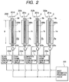
- Fig. 2 is a block diagram showing the details of the image forming units Pa, Pb, Pc and Pd shown in Fig. 1.
- the exposure means 8a, 8b, 8c and 8d positioned respectively corresponding to the photosensitive drums 1a, 1b, 1c and 1d are provided respectively with a light emission element array 200a for yellow, a light emission element array 200b for magenta, a light emission element array 200c for cyan and a light emission element array 200d for black, which are respectively connected a yellow signal drive circuit (IC) 202a, a magenta signal drive circuit (IC) 202b, a cyan signal drive circuit (IC) 202c and a black signal drive circuit (IC) 202d through wiring units 201a, 201b, 201c and 201d including lead wires arranged with a high density, whereby each light emission element is controlled in a light emitting state or a light non-emitting state by the function of the drive circuit.
- IC yellow signal drive circuit
- IC magenta signal drive circuit
- IC cyan signal drive circuit
- IC black signal drive circuit
- the light emitting operations of the light emission element arrays are controlled according to the image signals from a yellow signal generation circuit 204a, a magenta signal generation circuit 204b, a cyan signal generation circuit 204c and a black signal generation circuit 204d.
- the light emitting elements employed in the above-mentioned yellow, magenta, cyan and black light emission element arrays 200a, 200b, 200c and 200d form a linearly arrayed member (an arrayed member on a row or a column) with a high resolution of, for example, 1,200 dpi.
- a counter electrode provided in each of the yellow light emission element array 200a, magenta light emission element array 200b, cyan light emission element array 200c and black light emission element array 200d is utilized as a common electrode, and the timing of respective driving operations is controlled by a yellow common drive circuit 203a, a magenta common drive circuit 203b, a cyan common drive circuit 203c and a black common drive circuit 203d.
- the common driving operations, as well as the yellow, magenta, cyan and black image signals, are controlled by an image information processing unit 205 in a CPU (not shown).
- each of the yellow light emission element array 200a, magenta light emission element array 200b, cyan light emission element array 200c and black light emission element array 200d of the present invention there is employed a single-chip (one-chip) light emission element array so positioned as to cover the entire main scanning distance D in the main scanning direction relative to the rotating displacement of the photosensitive drum 1a, 1b, 1c or 1d.
- a single-chip (one-chip) light emission element array so positioned as to cover the entire main scanning distance D in the main scanning direction relative to the rotating displacement of the photosensitive drum 1a, 1b, 1c or 1d.
- light emitting elements are integrated on a single chip with a high resolution in excess of 600 dpi, such as 1,200 dpi or even higher, so that the single chip covers the entire main scanning distance D of the photosensitive member.
- the above-described single-chip light emission element arrays employed in the yellow, magenta, cyan and black light emission element arrays 200a, 200b, 200c and 200d are formed on a single substrate and are then cut into four units as will explained in the following.
- arrows C indicate the sub scanning direction of the rotating photosensitive members.
- the photosensitive drums 1a, 1b, 1c and 1d are composed of aluminum pipes of a same diameter (for example a diameter of 60, 30 or 20 cm) and are provided with a same organic photoconductive layer or an a-Si photosensitive layer, so that they have a same moving speed in the sub scanning direction C.
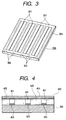
- Fig. 3 is a perspective view of a single-chip light emission element array substrate 300 provided on a single glass substrate 303 at a prior step in which single-chip light emission element arrays 301 employed in the above-described yellow, magenta, cyan and black light emission element arrays 200a, 200b, 200c and 200d shown in Fig. 2 have not been cut into four arrays along separation lines 302.
- the glass substrate 303 to be employed in the present invention may have any size as long as the light emission element arrays can be formed in a single chip.
- Fig. 4 is a cross-sectional view of the single-chip light emission element array 301 in the longitudinal direction thereof, in the single-chip light emission element array substrate 300 on the glass substrate 303 shown in Fig. 3.
- Each light emitting element is composed of a segment electrode 403, a counter electrode 402 and a light emitting layer 401 provided between the paired electrodes 402 and 403.
- an insulating layer (not shown) can be provided between the segment electrode 403 and the light emitting layer 401 or between the counter electrode 402 and the light emitting layer 401.
- the counter electrode 402 is used as a common electrode for applying a common signal
- the segment electrode 403 is used as an information signal electrode for applying an image signal.
- the light emitting elements on a single substrate are covered by a protective layer 404, and a sealant 405 is provided for mutually separating the light emitting elements.
- the light emitting layer 401 of the light emitting elements of the present invention is preferably composed of an organic electroluminescent (EL) light emitting element, but it can also be composed of an inorganic EL element.
- EL organic electroluminescent
- Examples of the materials constituting the organic EL to be employed in the present invention include those disclosed in EP-A-349,265 (1990) assigned to Scozzafava; U.S. Patent No. 4,356,429 assigned to Tang.; U.S. Patent No. 4,539,507 assigned to VanSlyke et al.; U.S. Patent No. 4,720,432 assigned to VanSlyke et al.; U.S. Patent No. 4,769,292 assigned to Tang et al.; U.S. Patent No. 4,885,211 assigned to Tang et al.; U.S. Patent No. 4,950,950 assigned to Perry et al.; U.S. Patent No.
- the EL layer is composed of an organic hole injection/transfer layer in contact with an anode, and an electron injection/transfer layer which forms a junction with the organic hole injection/transfer layer.
- the hole injection/transfer layer is formed by a single material or plural materials, and is composed of a hole injection layer which is in contact with an anode and with a continuous hole transfer layer provided between the hole injection layer and an electron injection/transfer layer.
- the electron injection/transfer layer is formed by a single material or a plurality of materials, and is composed of an electron injection layer which is in contact with the anode and with a continuous electron transfer layer provided between the electron injection layer and the hole injection/transfer layer.
- the hole-electron recombination and luminescence take place in the electron injection/transfer layer, adjacent to the junction between the electron injection/transfer layer and the hole injection/transfer layer.
- the compound constituting the organic EL layer is typically deposited by evaporation, but it can also be deposited by other known methods.
- the organic material constituting the hole injection layer has the following general formula: wherein:
- the hole transfer layer is composed of an aromatic tertiary amine, of which a preferred sub class includes tetraaryldiamine represented by the following formula: wherein Are is an arylene radical; n is an integer of from 1 to 4; and AR, R 7 , R 8 and R 9 are independently each other selected aryl radicals.
- the luminescent electron injection/transfer layer contains a metal oxinoid compound, of which preferred examples are represented by the following general formula: wherein R 2 to R 7 respectively mean possible substituents.
- the metal oxinoid compound is represented by the following formula: wherein R 2 to R 7 have the same meaning as defined above; and L 1 to L 5 represent independently each other a hydrogen atom or a hydrocarbon radical containing 1 to 12 carbon atoms, and L 1 and L 2 or L 2 and L 3 together may form a fused benzo ring.
- the metal oxinoid compound is represented by the following formula: wherein R 2 to R 6 respectively represent a hydrogen atom or a possible substituent.
- the examples described above merely represent the preferred organic material that can be employed in the electroluminescent layer. Such examples are not intended to limit the scope of the present invention but merely designate the organic electroluminescent layer in general sense.
- the organic EL material contains a coordinate compound having an organic ligand.
- the segment electrode 403 to be employed in the light emitting element of the present invention can be composed of reflective metal such as aluminum, silver, zinc, gold or chromium, and the counter electrode 402 can be composed of a transparent conductive film such as Indium Tin Oxide (ITO) or tin oxide.
- ITO Indium Tin Oxide
- the sealant 405 to be employed in the present invention can be composed of inorganic insulating substance such as silicon oxide or silicon nitride, or organic insulating resin such as epoxy resin.
- the protective film 404 to be employed in the present invention can be composed of a film of an inorganic insulating substance such as silicon oxide or silicon nitride, or organic insulating resin such as epoxy resin.
- the photosensitive layer of the photosensitive members 1a, 1b, 1c and 1d can be composed of an organic photoconductive substance such as photosensitive benzoxazols, photosensitive benzothiazols or photosensitive triphenylamines, or an inorganic photoconductive substance such as photosensitive amorphous silicon (a-Si), photosensitive amorphous silicon-germanium (a-SiGe) alloys or photosensitive amorphous silicon carbide (a-SiC).
- an organic photoconductive substance such as photosensitive benzoxazols, photosensitive benzothiazols or photosensitive triphenylamines
- an inorganic photoconductive substance such as photosensitive amorphous silicon (a-Si), photosensitive amorphous silicon-germanium (a-SiGe) alloys or photosensitive amorphous silicon carbide (a-SiC).
- the protective film (404) was prepared by sputtering silicon nitride in a thickness of 150 nm. The steps from the formation of the organic layer to the formation of the protective layer were executed in a same vacuum chamber.
- anode of the organic LED there is preferably used a material with a large work function, and may be used, in addition to ITO employed in the present embodiment, for example, tin oxide, gold, platinum, palladium, selenium, iridium or copper iodide.
- the cathode there is preferably used a material with a small work function, and may be used, in addition to Mg/Ag employed in the present embodiment, for example, Mg, Al, Li, In or alloys thereof.
- hole transport layer there may be used, in addition to TPD, any of the organic substances shown in the following Table 1.
- an inorganic substance such as a-Si or a-SiC.
- the electron transport layer there may be used, in addition to Alq 3 , any of the substances shown in the following Table 2.
- the electron transport layer or the hole transport layer may be doped with a dopant dye shown in the following Table 3.
- the material constituting the organic LED desirably has a light emission spectrum matching the sensitivity of the photosensitive drum to be used.
- a metal mask with a line width of 50 ⁇ m and a line pitch of 80 ⁇ m was placed and ITO was sputtered with a thickness of 100 nm to form the anode 403.
- the transparent substrate was then subjected to UV ion rinsing treatment for 30 minutes at 150°C.
- N,N'-bis(3-methylphenyl)-N,N'-diphenyl-(1,1'-biphenyl)-4,4'-diamine (hereinafter represented as TPD) as the hole transport layer and tris(8-quinolynol)aluminum (hereinafter represented as Alq 3 ) as the electron transport layer were deposited by vacuum deposition with respective thicknesses of 50 nm in this order.
- the vacuum deposition was executed under vacuum of 1 ⁇ 10 -6 torr and with a film forming rate of 0.3 nm/sec.
- the organic layer 401 was formed in the above-explained manner.
- the film forming rate was 1 nm/sec.
- the single-chip light emission element array substrate 300 prepared in this manner was then cut along the separation lines 302 shown in Fig. 3 to obtain four single-chip light emission element arrays 301 each having a size of 230 mm ⁇ 10 mm. Then a cover glass of a dimension of 220 mm ⁇ 5 mm ⁇ 0.5 mm was placed on the elements and was sealed with epoxy resin.
- the steps from the cutting to the sealing were executed in a nitrogen atmosphere.
- the single-chip light emission element array thus prepared was connected to a driver and was given a DC voltage, with the positive side at the ITO electrode and the negative side at the Mg/Ag electrode, whereby green light was emitted from the intersection of the ITO electrode and the Mg/Ag electrode.
- the four single-chip light emission element arrays thus prepared were measured as to a fluctuation in the amount of light emission among the pixels.
- the fluctuation in the amount of light emission from each pixels of a single-chip light emission element array was within ⁇ 3%, and the fluctuation in the amount of light emission among the four single-chip light emission element arrays was also within ⁇ 3%.
- the present invention employs the novel single-chip light emission element arrays instead of the conventional jointed LED's, thereby reducing the cost of the light emission element array in the image forming apparatus, and improving the color reproducibility in the main scanning direction. Also, since the four single-chip light emission element arrays provided respectively corresponding to the photosensitive members are taken from a single substrate and have therefore substantially equal light emission characteristics, the compensation of the characteristics among the different element arrays can be dispensed with and the cost required therefor can be significantly reduced.
Landscapes
- Physics & Mathematics (AREA)
- Optics & Photonics (AREA)
- Health & Medical Sciences (AREA)
- General Health & Medical Sciences (AREA)
- Toxicology (AREA)
- Printers Or Recording Devices Using Electromagnetic And Radiation Means (AREA)
- Electroluminescent Light Sources (AREA)
- Color Electrophotography (AREA)
Applications Claiming Priority (3)
| Application Number | Priority Date | Filing Date | Title |
|---|---|---|---|
| JP30861297A JPH11138899A (ja) | 1997-11-11 | 1997-11-11 | 画像形成装置 |
| JP308612/97 | 1997-11-11 | ||
| JP30861297 | 1997-11-11 |
Publications (2)
| Publication Number | Publication Date |
|---|---|
| EP0916506A2 true EP0916506A2 (fr) | 1999-05-19 |
| EP0916506A3 EP0916506A3 (fr) | 1999-09-08 |
Family
ID=17983151
Family Applications (1)
| Application Number | Title | Priority Date | Filing Date |
|---|---|---|---|
| EP98309346A Withdrawn EP0916506A3 (fr) | 1997-11-11 | 1998-11-10 | Appareil de formation d'image |
Country Status (3)
| Country | Link |
|---|---|
| US (1) | US6236416B1 (fr) |
| EP (1) | EP0916506A3 (fr) |
| JP (1) | JPH11138899A (fr) |
Cited By (7)
| Publication number | Priority date | Publication date | Assignee | Title |
|---|---|---|---|---|
| DE10001914A1 (de) * | 2000-01-19 | 2001-07-26 | Heidelberger Druckmasch Ag | Verfahren und Vorrichtung zum Belichten von fotoempfindlichem Material |
| EP1324156A1 (fr) * | 2001-12-25 | 2003-07-02 | Seiko Epson Corporation | Appareil de formation d'images avec une tête d'exposition à matrice organique électroluminescente |
| US6731322B2 (en) * | 2000-06-14 | 2004-05-04 | Fuji Photo Film Co., Ltd. | Exposing apparatus |
| WO2004051382A3 (fr) * | 2002-12-05 | 2004-11-18 | Matsushita Electric Industrial Co Ltd | Appareil de formation d'images |
| US6844945B2 (en) | 2001-11-30 | 2005-01-18 | Dai Nippon Printing Co., Ltd. | Hologram having authenticating information recorded therein |
| EP1564006A3 (fr) * | 2004-02-16 | 2008-03-05 | Seiko Epson Corporation | Tête linéaire et machine à formation d'images utilisant cette tête |
| EP3007243A3 (fr) * | 2001-01-15 | 2016-06-15 | Sony Corporation | Dispositif électroluminescent et son procédé de production |
Families Citing this family (7)
| Publication number | Priority date | Publication date | Assignee | Title |
|---|---|---|---|---|
| JP3626728B2 (ja) * | 2000-05-23 | 2005-03-09 | 長瀬産業株式会社 | 有機elディスプレイ及び有機elディスプレイの製造方法 |
| CN100423532C (zh) * | 2001-08-09 | 2008-10-01 | 松下电器产业株式会社 | 图像读取装置的光源以及光源的驱动装置 |
| CN1262897C (zh) | 2002-08-06 | 2006-07-05 | 精工爱普生株式会社 | 图像载体盒及使用该图像载体盒的图像形成装置 |
| CN1282909C (zh) | 2002-08-09 | 2006-11-01 | 精工爱普生株式会社 | 曝光头及使用该曝光头的图像形成装置 |
| EP1598199A3 (fr) | 2004-05-20 | 2009-05-06 | Seiko Epson Corporation | Tête en ligne et dispositif de formation d'images comprenent cette tête |
| US7486306B2 (en) | 2004-11-29 | 2009-02-03 | Seiko Epson Corporation | Optical writing device and method of manufacturing the same |
| US7663653B2 (en) | 2005-02-24 | 2010-02-16 | Seiko Epson Corporation | Optical head and image forming apparatus incorporating the same |
Citations (8)
| Publication number | Priority date | Publication date | Assignee | Title |
|---|---|---|---|---|
| US4356429A (en) | 1980-07-17 | 1982-10-26 | Eastman Kodak Company | Organic electroluminescent cell |
| US4539507A (en) | 1983-03-25 | 1985-09-03 | Eastman Kodak Company | Organic electroluminescent devices having improved power conversion efficiencies |
| US4720432A (en) | 1987-02-11 | 1988-01-19 | Eastman Kodak Company | Electroluminescent device with organic luminescent medium |
| US4769292A (en) | 1987-03-02 | 1988-09-06 | Eastman Kodak Company | Electroluminescent device with modified thin film luminescent zone |
| US4885211A (en) | 1987-02-11 | 1989-12-05 | Eastman Kodak Company | Electroluminescent device with improved cathode |
| EP0349265A2 (fr) | 1988-06-27 | 1990-01-03 | EASTMAN KODAK COMPANY (a New Jersey corporation) | Dispositifs électroluminescentes |
| US4950950A (en) | 1989-05-18 | 1990-08-21 | Eastman Kodak Company | Electroluminescent device with silazane-containing luminescent zone |
| US5059861A (en) | 1990-07-26 | 1991-10-22 | Eastman Kodak Company | Organic electroluminescent device with stabilizing cathode capping layer |
Family Cites Families (26)
| Publication number | Priority date | Publication date | Assignee | Title |
|---|---|---|---|---|
| JPS5714058A (en) * | 1980-06-28 | 1982-01-25 | Ricoh Co Ltd | Printer |
| US4721977A (en) * | 1984-11-26 | 1988-01-26 | Kentek Information Systems, Inc. | Electrographic printer with abutting chips each having an array of charge-discharging elements |
| EP0238095A1 (fr) * | 1986-03-20 | 1987-09-23 | Minolta Camera Kabushiki Kaisha | Membre photosensible composé d'une couche transporteuse de charge et d'une couche génératrice de charge |
| GB8722946D0 (en) * | 1987-09-30 | 1987-11-04 | Plessey Co Plc | Light emitting diode array |
| EP0335553B1 (fr) | 1988-03-18 | 1999-09-15 | Nippon Sheet Glass Co., Ltd. | Matrice d'éléments émetteurs de lumière à autobalayage |
| US5257049A (en) | 1990-07-03 | 1993-10-26 | Agfa-Gevaert N.V. | LED exposure head with overlapping electric circuits |
| US5047687A (en) | 1990-07-26 | 1991-09-10 | Eastman Kodak Company | Organic electroluminescent device with stabilized cathode |
| US5059862A (en) | 1990-07-26 | 1991-10-22 | Eastman Kodak Company | Electroluminescent device with improved cathode |
| US5073446A (en) | 1990-07-26 | 1991-12-17 | Eastman Kodak Company | Organic electroluminescent device with stabilizing fused metal particle cathode |
| US5061617A (en) | 1990-12-07 | 1991-10-29 | Eastman Kodak Company | Process for the preparation of high chloride tabular grain emulsions |
| US5151629A (en) | 1991-08-01 | 1992-09-29 | Eastman Kodak Company | Blue emitting internal junction organic electroluminescent device (I) |
| US5300961A (en) | 1991-12-16 | 1994-04-05 | Xerox Corporation | Method and apparatus for aligning multiple print bars in a single pass system |
| US5294869A (en) | 1991-12-30 | 1994-03-15 | Eastman Kodak Company | Organic electroluminescent multicolor image display device |
| US5294870A (en) | 1991-12-30 | 1994-03-15 | Eastman Kodak Company | Organic electroluminescent multicolor image display device |
| DE4303225C2 (de) * | 1993-02-04 | 1996-08-14 | Siemens Nixdorf Inf Syst | Optischer Zeichengenerator für einen elektrografischen Drucker |
| US5339150A (en) | 1993-03-23 | 1994-08-16 | Xerox Corporation | Mark detection circuit for an electrographic printing machine |
| JPH06302855A (ja) | 1993-03-29 | 1994-10-28 | Minnesota Mining & Mfg Co <3M> | 光学走査装置 |
| JPH07140753A (ja) | 1993-11-19 | 1995-06-02 | Fujitsu Ltd | カラー画像形成装置 |
| JPH07314771A (ja) | 1994-05-20 | 1995-12-05 | Sharp Corp | Led書込装置 |
| JPH0848052A (ja) * | 1994-08-09 | 1996-02-20 | Oki Electric Ind Co Ltd | Elアレイを有する光プリンタヘッド |
| JP3452982B2 (ja) * | 1994-08-24 | 2003-10-06 | ローム株式会社 | Ledプリントヘッド、およびledアレイチップ、ならびにそのledアレイチップの製造方法 |
| JPH0890832A (ja) | 1994-09-27 | 1996-04-09 | Oki Electric Ind Co Ltd | 発光素子アレイおよび光学ヘッド |
| JP3385134B2 (ja) * | 1994-11-14 | 2003-03-10 | 株式会社沖データ | 電子写真記録装置 |
| JP3194423B2 (ja) * | 1996-05-30 | 2001-07-30 | キヤノン株式会社 | 画像形成装置 |
| JP3703234B2 (ja) * | 1996-12-24 | 2005-10-05 | キヤノン株式会社 | 画像記録装置 |
| JP2942230B2 (ja) * | 1998-01-12 | 1999-08-30 | キヤノン株式会社 | 画像形成装置及び発光装置 |
-
1997
- 1997-11-11 JP JP30861297A patent/JPH11138899A/ja active Pending
-
1998
- 1998-11-06 US US09/187,398 patent/US6236416B1/en not_active Expired - Lifetime
- 1998-11-10 EP EP98309346A patent/EP0916506A3/fr not_active Withdrawn
Patent Citations (8)
| Publication number | Priority date | Publication date | Assignee | Title |
|---|---|---|---|---|
| US4356429A (en) | 1980-07-17 | 1982-10-26 | Eastman Kodak Company | Organic electroluminescent cell |
| US4539507A (en) | 1983-03-25 | 1985-09-03 | Eastman Kodak Company | Organic electroluminescent devices having improved power conversion efficiencies |
| US4720432A (en) | 1987-02-11 | 1988-01-19 | Eastman Kodak Company | Electroluminescent device with organic luminescent medium |
| US4885211A (en) | 1987-02-11 | 1989-12-05 | Eastman Kodak Company | Electroluminescent device with improved cathode |
| US4769292A (en) | 1987-03-02 | 1988-09-06 | Eastman Kodak Company | Electroluminescent device with modified thin film luminescent zone |
| EP0349265A2 (fr) | 1988-06-27 | 1990-01-03 | EASTMAN KODAK COMPANY (a New Jersey corporation) | Dispositifs électroluminescentes |
| US4950950A (en) | 1989-05-18 | 1990-08-21 | Eastman Kodak Company | Electroluminescent device with silazane-containing luminescent zone |
| US5059861A (en) | 1990-07-26 | 1991-10-22 | Eastman Kodak Company | Organic electroluminescent device with stabilizing cathode capping layer |
Cited By (8)
| Publication number | Priority date | Publication date | Assignee | Title |
|---|---|---|---|---|
| DE10001914A1 (de) * | 2000-01-19 | 2001-07-26 | Heidelberger Druckmasch Ag | Verfahren und Vorrichtung zum Belichten von fotoempfindlichem Material |
| US6731322B2 (en) * | 2000-06-14 | 2004-05-04 | Fuji Photo Film Co., Ltd. | Exposing apparatus |
| EP3007243A3 (fr) * | 2001-01-15 | 2016-06-15 | Sony Corporation | Dispositif électroluminescent et son procédé de production |
| US6844945B2 (en) | 2001-11-30 | 2005-01-18 | Dai Nippon Printing Co., Ltd. | Hologram having authenticating information recorded therein |
| EP1324156A1 (fr) * | 2001-12-25 | 2003-07-02 | Seiko Epson Corporation | Appareil de formation d'images avec une tête d'exposition à matrice organique électroluminescente |
| WO2004051382A3 (fr) * | 2002-12-05 | 2004-11-18 | Matsushita Electric Industrial Co Ltd | Appareil de formation d'images |
| US7116345B2 (en) | 2002-12-05 | 2006-10-03 | Matsushita Electric Industrial Co., Ltd. | Image forming apparatus having a cooler for an organic electroluminescence element |
| EP1564006A3 (fr) * | 2004-02-16 | 2008-03-05 | Seiko Epson Corporation | Tête linéaire et machine à formation d'images utilisant cette tête |
Also Published As
| Publication number | Publication date |
|---|---|
| JPH11138899A (ja) | 1999-05-25 |
| EP0916506A3 (fr) | 1999-09-08 |
| US6236416B1 (en) | 2001-05-22 |
Similar Documents
| Publication | Publication Date | Title |
|---|---|---|
| JP2942230B2 (ja) | 画像形成装置及び発光装置 | |
| EP0916506A2 (fr) | Appareil de formation d'image | |
| US6504565B1 (en) | Light-emitting device, exposure device, and image forming apparatus | |
| US6794816B2 (en) | Organic EL panel and the manufacture thereof | |
| EP1009046B1 (fr) | Rangée d'éléments à électroluminescence, procédé de fabrication de la rangée et appareil de formation d'images | |
| US6573920B2 (en) | Method of manufacturing a printer with an electroluminescent (EL) pixel array | |
| US8427517B2 (en) | Light-emitting element, exposure head and image-forming apparatus | |
| JP3039778B2 (ja) | 画像形成装置 | |
| JP2000277253A (ja) | 発光素子、発光装置、表示装置、露光装置及び画像形成装置 | |
| JP2000082720A (ja) | 発光装置、露光装置及び画像形成装置 | |
| JP3631074B2 (ja) | 発光装置 | |
| JPH0695456A (ja) | 画像形成装置 | |
| JP4143180B2 (ja) | 多色画像形成装置 | |
| JP4154045B2 (ja) | 画像形成装置 | |
| JP2007210277A (ja) | 露光装置および画像形成装置 | |
| JP4639918B2 (ja) | ラインヘッド、及び画像形成装置 | |
| JP4541535B2 (ja) | 光ヘッド用有機発光ダイオードアレイ | |
| EP4632491A2 (fr) | Appareil de formation d'images | |
| JPS59102259A (ja) | 電子写真記録装置 | |
| JP2000127491A (ja) | 露光装置及び画像形成装置 | |
| JP2000289249A (ja) | 露光装置及びそれを用いた画像形成装置 | |
| JPH08244272A (ja) | 光プリンタヘッド | |
| JPH0848052A (ja) | Elアレイを有する光プリンタヘッド | |
| JP2007283491A (ja) | 発光素子、この発光素子を用いた発光装置、光ヘッド及び画像形成装置 | |
| JP3302329B2 (ja) | 発光装置、露光装置及び画像形成装置 |
Legal Events
| Date | Code | Title | Description |
|---|---|---|---|
| PUAI | Public reference made under article 153(3) epc to a published international application that has entered the european phase |
Free format text: ORIGINAL CODE: 0009012 |
|
| AK | Designated contracting states |
Kind code of ref document: A2 Designated state(s): DE FR GB NL |
|
| AX | Request for extension of the european patent |
Free format text: AL;LT;LV;MK;RO;SI |
|
| PUAL | Search report despatched |
Free format text: ORIGINAL CODE: 0009013 |
|
| AK | Designated contracting states |
Kind code of ref document: A3 Designated state(s): AT BE CH CY DE DK ES FI FR GB GR IE IT LI LU MC NL PT SE |
|
| AX | Request for extension of the european patent |
Free format text: AL;LT;LV;MK;RO;SI |
|
| RIC1 | Information provided on ipc code assigned before grant |
Free format text: 6B 41J 2/45 A, 6G 03G 5/07 B |
|
| 17P | Request for examination filed |
Effective date: 20000121 |
|
| AKX | Designation fees paid |
Free format text: DE FR GB NL |
|
| 17Q | First examination report despatched |
Effective date: 20030218 |
|
| STAA | Information on the status of an ep patent application or granted ep patent |
Free format text: STATUS: THE APPLICATION IS DEEMED TO BE WITHDRAWN |
|
| 18D | Application deemed to be withdrawn |
Effective date: 20030701 |