EP1065533A2 - Filtre couleur et son procédé de fabrication - Google Patents
Filtre couleur et son procédé de fabrication Download PDFInfo
- Publication number
- EP1065533A2 EP1065533A2 EP00305514A EP00305514A EP1065533A2 EP 1065533 A2 EP1065533 A2 EP 1065533A2 EP 00305514 A EP00305514 A EP 00305514A EP 00305514 A EP00305514 A EP 00305514A EP 1065533 A2 EP1065533 A2 EP 1065533A2
- Authority
- EP
- European Patent Office
- Prior art keywords
- picture element
- photocatalyst
- ink
- element part
- containing layer
- Prior art date
- Legal status (The legal status is an assumption and is not a legal conclusion. Google has not performed a legal analysis and makes no representation as to the accuracy of the status listed.)
- Granted
Links
Images



Classifications
-
- G—PHYSICS
- G02—OPTICS
- G02B—OPTICAL ELEMENTS, SYSTEMS OR APPARATUS
- G02B5/00—Optical elements other than lenses
- G02B5/20—Filters
-
- G—PHYSICS
- G02—OPTICS
- G02B—OPTICAL ELEMENTS, SYSTEMS OR APPARATUS
- G02B5/00—Optical elements other than lenses
- G02B5/20—Filters
- G02B5/201—Filters in the form of arrays
-
- B—PERFORMING OPERATIONS; TRANSPORTING
- B82—NANOTECHNOLOGY
- B82Y—SPECIFIC USES OR APPLICATIONS OF NANOSTRUCTURES; MEASUREMENT OR ANALYSIS OF NANOSTRUCTURES; MANUFACTURE OR TREATMENT OF NANOSTRUCTURES
- B82Y10/00—Nanotechnology for information processing, storage or transmission, e.g. quantum computing or single electron logic
-
- B—PERFORMING OPERATIONS; TRANSPORTING
- B82—NANOTECHNOLOGY
- B82Y—SPECIFIC USES OR APPLICATIONS OF NANOSTRUCTURES; MEASUREMENT OR ANALYSIS OF NANOSTRUCTURES; MANUFACTURE OR TREATMENT OF NANOSTRUCTURES
- B82Y40/00—Manufacture or treatment of nanostructures
-
- G—PHYSICS
- G02—OPTICS
- G02B—OPTICAL ELEMENTS, SYSTEMS OR APPARATUS
- G02B5/00—Optical elements other than lenses
- G02B5/20—Filters
- G02B5/22—Absorbing filters
- G02B5/223—Absorbing filters containing organic substances, e.g. dyes, inks or pigments
-
- G—PHYSICS
- G03—PHOTOGRAPHY; CINEMATOGRAPHY; ANALOGOUS TECHNIQUES USING WAVES OTHER THAN OPTICAL WAVES; ELECTROGRAPHY; HOLOGRAPHY
- G03F—PHOTOMECHANICAL PRODUCTION OF TEXTURED OR PATTERNED SURFACES, e.g. FOR PRINTING, FOR PROCESSING OF SEMICONDUCTOR DEVICES; MATERIALS THEREFOR; ORIGINALS THEREFOR; APPARATUS SPECIALLY ADAPTED THEREFOR
- G03F7/00—Photomechanical, e.g. photolithographic, production of textured or patterned surfaces, e.g. printing surfaces; Materials therefor, e.g. comprising photoresists; Apparatus specially adapted therefor
- G03F7/0005—Production of optical devices or components in so far as characterised by the lithographic processes or materials used therefor
- G03F7/0007—Filters, e.g. additive colour filters; Components for display devices
-
- B—PERFORMING OPERATIONS; TRANSPORTING
- B41—PRINTING; LINING MACHINES; TYPEWRITERS; STAMPS
- B41J—TYPEWRITERS; SELECTIVE PRINTING MECHANISMS, i.e. MECHANISMS PRINTING OTHERWISE THAN FROM A FORME; CORRECTION OF TYPOGRAPHICAL ERRORS
- B41J2202/00—Embodiments of or processes related to ink-jet or thermal heads
- B41J2202/01—Embodiments of or processes related to ink-jet heads
- B41J2202/09—Ink jet technology used for manufacturing optical filters
-
- G—PHYSICS
- G02—OPTICS
- G02F—OPTICAL DEVICES OR ARRANGEMENTS FOR THE CONTROL OF LIGHT BY MODIFICATION OF THE OPTICAL PROPERTIES OF THE MEDIA OF THE ELEMENTS INVOLVED THEREIN; NON-LINEAR OPTICS; FREQUENCY-CHANGING OF LIGHT; OPTICAL LOGIC ELEMENTS; OPTICAL ANALOGUE/DIGITAL CONVERTERS
- G02F1/00—Devices or arrangements for the control of the intensity, colour, phase, polarisation or direction of light arriving from an independent light source, e.g. switching, gating or modulating; Non-linear optics
- G02F1/01—Devices or arrangements for the control of the intensity, colour, phase, polarisation or direction of light arriving from an independent light source, e.g. switching, gating or modulating; Non-linear optics for the control of the intensity, phase, polarisation or colour
- G02F1/13—Devices or arrangements for the control of the intensity, colour, phase, polarisation or direction of light arriving from an independent light source, e.g. switching, gating or modulating; Non-linear optics for the control of the intensity, phase, polarisation or colour based on liquid crystals, e.g. single liquid crystal display cells
- G02F1/133—Constructional arrangements; Operation of liquid crystal cells; Circuit arrangements
- G02F1/1333—Constructional arrangements; Manufacturing methods
- G02F1/1335—Structural association of cells with optical devices, e.g. polarisers or reflectors
- G02F1/133509—Filters, e.g. light shielding masks
- G02F1/133512—Light shielding layers, e.g. black matrix
-
- G—PHYSICS
- G02—OPTICS
- G02F—OPTICAL DEVICES OR ARRANGEMENTS FOR THE CONTROL OF LIGHT BY MODIFICATION OF THE OPTICAL PROPERTIES OF THE MEDIA OF THE ELEMENTS INVOLVED THEREIN; NON-LINEAR OPTICS; FREQUENCY-CHANGING OF LIGHT; OPTICAL LOGIC ELEMENTS; OPTICAL ANALOGUE/DIGITAL CONVERTERS
- G02F1/00—Devices or arrangements for the control of the intensity, colour, phase, polarisation or direction of light arriving from an independent light source, e.g. switching, gating or modulating; Non-linear optics
- G02F1/01—Devices or arrangements for the control of the intensity, colour, phase, polarisation or direction of light arriving from an independent light source, e.g. switching, gating or modulating; Non-linear optics for the control of the intensity, phase, polarisation or colour
- G02F1/13—Devices or arrangements for the control of the intensity, colour, phase, polarisation or direction of light arriving from an independent light source, e.g. switching, gating or modulating; Non-linear optics for the control of the intensity, phase, polarisation or colour based on liquid crystals, e.g. single liquid crystal display cells
- G02F1/133—Constructional arrangements; Operation of liquid crystal cells; Circuit arrangements
- G02F1/1333—Constructional arrangements; Manufacturing methods
- G02F1/1335—Structural association of cells with optical devices, e.g. polarisers or reflectors
- G02F1/133509—Filters, e.g. light shielding masks
- G02F1/133514—Colour filters
- G02F1/133516—Methods for their manufacture, e.g. printing, electro-deposition or photolithography
-
- G—PHYSICS
- G03—PHOTOGRAPHY; CINEMATOGRAPHY; ANALOGOUS TECHNIQUES USING WAVES OTHER THAN OPTICAL WAVES; ELECTROGRAPHY; HOLOGRAPHY
- G03F—PHOTOMECHANICAL PRODUCTION OF TEXTURED OR PATTERNED SURFACES, e.g. FOR PRINTING, FOR PROCESSING OF SEMICONDUCTOR DEVICES; MATERIALS THEREFOR; ORIGINALS THEREFOR; APPARATUS SPECIALLY ADAPTED THEREFOR
- G03F7/00—Photomechanical, e.g. photolithographic, production of textured or patterned surfaces, e.g. printing surfaces; Materials therefor, e.g. comprising photoresists; Apparatus specially adapted therefor
- G03F7/0002—Lithographic processes using patterning methods other than those involving the exposure to radiation, e.g. by stamping
Definitions
- the present invention relates to a color filter which is obtained by coloring a picture element part with an ink jet system and which is suitable for a color liquid crystal display and a process for producing the same.
- a liquid crystal usually operates as a shutter by equipping with three primary colors of red (R), green (G) and blue (B) and switching ON and OFF of an electrode corresponding to each picture element part of R, G and B and the color display is performed by transmission of the light through each picture element part of R, G and B.
- a dyeing process As a process for producing a color filter which has hitherto been carried out, there is, for example, a dyeing process.
- a water-soluble polymer material which is a material for dyeing is first formed on a glass substrate, which is patterned into the desired shape by a photolithography step and the resulting pattern is dipped into a dyeing bath to obtain a colored pattern. This is repeated three times to form a color filter layer consisting of picture element parts of R, G and B.
- a pigment dispersing method (color resist method).
- a photosensitive resin layer in which a pigment is dispersed is first formed on a substrate and this is subjected to patterning to obtain a monocolor pattern. Further, this step is repeated three times to form a color filter layer consist of picture element parts ofR, G and B.
- an electrode position method and a method of dispersing a pigment in a thermosetting resin and performing three times printing of R, G and B and, thereafter, thermally curing the resin are an electrode position method and a method of dispersing a pigment in a thermosetting resin and performing three times printing of R, G and B and, thereafter, thermally curing the resin.
- the same step needs to be repeated three times for coloring three colors of R, G and B, and there is a problem that the cost is high and a yield is decreased because of repetition of a step.
- JP-A-59-75205 a method of blowing a coloring ink with an ink jet system to form a colored layer (picture element part)
- JP-A-59-75205 a method of blowing a coloring ink with an ink jet system to form a colored layer (picture element part)
- a method for producing a color filter by forming a colored layer with an ink jet system there is described a method of forming a colored layer (picture element part) by providing an ink absorbing layer on a substrate and making a difference in the ink absorbability of this absorbing layer between an exposed part and an unexposed part in JP-A-8-230314 and JP-A-8-227012.
- a colored layer is formed by forming an absorbing layer and absorbing an ink in this absorbing layer, there is a problem that a difference in the coloration between a central part of an ink dot and a surrounding part of that is present which results in the color nonuniformity.
- this absorbing layer needs the predetermined thickness resulted from its function of absorbing an ink.
- a shading part called as a black matrix is generally provided on a boundary portion of a picture element part.
- the shading part generally formed on the side of color filter.
- the shading part is formed on the side of a substrate opposite to the color filter.
- a color filter in which a shading part is not provided is formed. The above-described problems also occur in the color filter which do not has a shading part.
- the present invention was done in view of the above problems and a main object thereof is to provide a color filter which do not have a shading part, in which a part having the better wettability and a part having the worse wettability can be formed on a single layer regarding the wettability of a substrate which becomes problematic upon formation of a picture element part with an ink jet system, and a pattern formed of the part having the better wettability and the part having the worse wettability can be formed in a few steps and, further, an ink absorbing layer is not necessary, and which has the better quality and which can be produced with the low cost, and a process for producing the same.
- the present invention provides a color filter which comprises a transparent substrate, a picture element part in which a plurality of colors are provided in the predetermined pattern with an ink jet system on the transparent substrate, and a wettability-variable layer being capable of varying the wettability which is provided for forming the picture element part.
- the present invention is characterized in that it has a wettability-variable layer in order to form a picture element part. Therefore, by utilizing the change in the wettability of a wettability-variable layer, a picture element part can be formed with the better precision, and a high quality color filter having no problem such as color missing and color nonuniformity can be provided.
- the construction may be such that the wettability-variable layer is provided on the transparent substrate, and the picture element part is provided on the wettability-variable layer.
- a wettability-variable layer of a part on which a picture element part is formed can be made to be an inkphilic region having a small contact angle with a liquid in advance, and the other part of the wettability-variable layer can be made to be an ink-repellent region having a large contact angle with a liquid.
- an ink is adhered to only the inkphilic region having a small contact angle with a liquid. Accordingly, the ink is applied uniformly within the whole surface of the picture element part. Therefore, a color filter having no disadvantage such as color nonuniformity and color missing can be provided.
- a space (distance) between the picture element parts is not more than 2 ⁇ m. Since a color filter of the present invention does not have a black matrix (shading part), when actually using for a liquid crystal panel, it is necessary to use together with a back light side substrate having a black-matrix. In this case, when a space between picture element parts is wide, it is necessary to have a high precision concerning positioning with the back light side substrate which has a black matrix. If it is not so, a back light penetrates the space between the picture element parts, as a result, the so-called color missing may occur.
- the space between the picture element parts is as small as possible, concretely, it is preferable that the space between the picture element parts is not more than 2 ⁇ m. Further, a colored layer consisting of the picture element parts can obtain surface smoothness if the space between the picture element parts is small like that.
- an ink-repellent convex part may be formed on a surface of a wettability-variable layer at a boundary portion of the picture element part. Since an ink-repellent convex part is formed on a boundary portion between the picture element parts forming portions when the picture element part is formed by adhering an ink with an ink jet system, the disadvantages such as mixing of inks during coloring, do not occur, being preferable.
- the construction may be such that the picture element part is provided on the transparent substrate, and the wettability-variable layer is provided on a border portion between the picture element parts.
- a wettability-variable layer of a border part of a picture element part an inkphilic region having the small contact angle with a liquid thereafter, covering the whole with a protecting layer can be easily carried out and, thus, a color filter having the high quality can be obtained.
- the wettability on the transparent substrate is less than 10 degrees in terms of the contact angle with a liquid having the surface tension of 40 mN/m. This is because, when an ink is adhered to the picture element part forming portion on the transparent substrate with an ink jet system, the ink for the picture element part is uniformly spread with a picture element part forming portion, the better-quality color filter having no disadvantages such as color nonuniformity and the like can be provided.
- the wettability-variable layer is a photocatalyst-containing layer comprising at least a photocatalyst and a binder, and having the wettability which varies so that the contact angle with a liquid is decreased by irradiation with the energy.
- the wettability of this layer can be varied by performing the pattern irradiation of the energy and the like and an inkphilic region having the small contact angle with a liquid can be formed easily and, for example, it becomes possible to easily make only a part on which a picture element part is formed into an inkphilic region. Accordingly, when a shading part is not provided between the picture element parts, the picture element part can be easily formed, and a color filter without a shading port can be manufactured effectively.
- the photocatalyst-containing layer contains fluorine and the photocatalyst-containing layer is formed so that the content of fluorine on the surface of the photocatalyst-containing layer is decreased by the action of the photocatalyst as compared with before the irradiation of the energy upon irradiating the photocatalyst-containing layer with the energy.
- a color filter of the present invention is constructed such that the fluorine content of the energy irradiated part on a photocatalyst-containing layer formed on a transparent substrate is decreased, a pattern comprising a part in which the fluorine content is decreased can be formed by the pattern-irradiation of the energy. Since when the fluorine content is decreased, the part becomes a region having the high inkphilicity as compared with other parts, it becomes possible to easily make only a part on which a picture element part and the like is formed an inkphilic region, and a color filter can be easily manufactured.
- the fluorine content of a part in which the fluorine content is decreased by irradiating the photocatalyst-containing layer with the energy is 10 or less relative to 100 of the fluorine content of a part which was not irradiated with the energy.
- the fluorine content of a part having the lower fluorine content which was formed by irradiating the photocatalyst-containing layer with the energy is 10 or less based on the weight relative to 100 of the fluorine content of a part which is not irradiated with the energy, a great difference in the inkphilicity between a part irradiated with the energy and a part not irradiated with the energy can be produced.
- the photocatalyst comprised in the photocatalyst-containing layer is preferably one or more selected from the group consisting of titanium oxide (TiO 2 ), zinc oxide (ZnO), tin oxide (SnO 2 ), strontium titanate (SrTiO 3 ), tungsten oxide (WO 3 ), bismuth oxide (Bi 2 O 3 ), and iron oxide (Fe 2 O 3 ).
- titanium oxide (TiO 2 ) is preferable. This is because since titanium oxide has the high band gap energy, it is effective as a photocatalyst, is chemically stable, has no toxicity and is easily available.
- a color filter in which a photocatalyst is titanium oxide
- a binder which is the other component constituting a photocatalyst-containing layer is preferably organopolysiloxane having a fluoroalkyl group.
- a color filter of the present invention as a method of inclusion of fluorine element in a photocatalyst-containing layer, mention may be made of various methods.
- organopolysiloxane having a fluoroalkyl group as a binder, fluorine element can be easily contained in a photocatalyst-containing layer and the content thereof can be easily reduced by the energy irradiation.
- a binder which is the other component constituting a photocatalyst-containing layer is formed of organopolysiloxane which is one or more of a hydrolyzed condensed compound or a co-hydrolyzed condensed compound of a silicon compound represented by Y n SiX (4-n) (wherein Y represents alkyl group, fluoroalkyl group, vinyl group, amino group, phenyl group or epoxy group, X represents alkoxy group or halogen, and n is an integer of 0 to 3).
- a silicon compound having a fluoroalkyl group among the aforementioned silicon compounds constituting the aforementioned organopolysiloxane is contained at an amount of not less than 0.01 mol%.
- the contact angle with a liquid having the surface tension of 40 mN/m on the photocatalyst-containing layer is 10 degrees or more in a part not irradiated with the energy and the angle is less than 10 degrees in a part irradiated with the energy. Since a part not irradiated with the energy is a part requiring the ink-repellent properties, when the contact angle with a liquid having the surface tension of 40 mN/m is less than 10 degrees, the ink-repellent properties are not sufficient and there is a possibility that an ink and a coating material for a shading part and the like remain, being not preferable.
- a picture element part colored with the aforementioned ink jet system is a picture element part colored with an ink jet system using an UV-curing ink. This is because, after a picture element part is colored with an ink jet system by using an-UV curing ink, UV is irradiated and, thereby, an ink can be rapidly cured, which can be sent to a next step, being preferable in a respect of the efficiency.
- a liquid crystal panel having the aforementioned color filter and a opposite substrate having a shading part, and which is obtained by encapsulating a liquid crystal compound between both substrates, has the advantages of the aforementioned color filter, that is, the advantages that color missing and color nonuniformity of a picture element part are not present and it is advantageous in a respect of cost.
- the present invention provides a process for production of a color filter, which comprises steps: (1) a step of providing a photocatalyst-containing layer having the wettability of the energy-irradiated part which changes in a direction of reduction of the contact angle with a liquid, on a transparent substrate, (2) a step of forming an exposed part for a picture element part by pattern-irradiating with the energy on a picture element part forming portion on which the picture element part, on the photocatalyst-containing layer formed on the transparent substrate, is to be formed, and (3) a step of coloring the exposed part for a picture element part with an ink jet system, to form a picture element part.
- a process for producing a color filter in the present invention by providing a photocatalyst-containing layer on a transparent substrate and irradiating this photocatalyst-containing layer with the energy, an exposed part for a picture element part, on which the contact angle with a liquid of the energy-irradiated part is reduced, can be formed.
- an exposed part for a picture element part on which the contact angle with a liquid of the energy-irradiated part is reduced, can be formed.
- the picture element part can be easily formed. Accordingly, it is possible to form the picture element part with the ink jet system with advantageous in a respect of cost even if there is no shading part on the transparent substrate.
- the step of forming an exposed part for a picture element part, then coloring the part with an ink jet system to form the picture element part may comprise steps; (a) a step of forming a exposed part for a first picture element part by pattern-irradiating with the energy on a part of a picture element part forming portion on which the picture element part, on the photocatalyst-containing layer, is to be formed, (b) a step of forming a first picture element part by coloring the exposed part for a first picture element part with the ink jet system, (c) a step of forming a exposed part for a second picture element part by irradiating with the energy on a remaining part of a picture element part forming portion on which the picture element part, on the photocatalyst-containing layer, is to be formed, and (d) a step of forming a second picture element part by coloring the exposed part for a second picture element part with the ink jet system.
- the adjacent picture element parts can be formed on apart positions each other during formation of the first picture element part because the energy can be pattern-irradiated such that the picture element part is formed alternately during formation of the first picture element part. Since the exposed part for a first picture element part is formed the condition such that relatively wide ink-repellent region exist between the colored regions, like that, and is colored with an ink jet system, there is no possibility of mixing some sorts of ink for adjacent picture element parts.
- the exposed part for a second picture element part is formed though exposing again between the first picture element parts formed like that, and then is colored with the ink jet system, as a result a color filter which do not have deficiency such as ink mixing, can be obtained. Further, concerning a color filter which do not have a shading part, there are some demands such that no space exist between picture element parts. In this case, it is necessary to employ the method such that the formation of picture element parts divides into two times, described above.
- an exposed part for an ink-repellent convex part where an ink-repellent convex part is to be formed may be formed before formation of the exposed part for a picture element part, and then an ink-repellent convex part may be formed on the exposed part for an ink-repellent convex part through using resin composition.
- an ink-repellent convex part like this, for example, when the ink-repellent convex part is formed around the region where a picture element part is to be formed, it is possible to prevent the problem such that a picture element part can not be formed precisely because ink flows out at the portion around a color filter.
- the present invention provides a process for production of a color filter, which comprises steps: (1) a step of providing a photocatalyst-containing layer having the wettability of the energy-irradiated part which changes in a direction of reduction of the contact angle with a liquid, at a boundary portion of a picture element part forming portion on which the picture element part is to be formed, on a transparent substrate, (2) a step of forming the picture element part on the picture element part forming portion on the transparent substrate.
- a photocatalyst-containing layer is provided at the boundary portion of the picture element part on the transparent substrate.
- the picture element part forming portion is an inkphilic region which has smaller contact angle with a liquid than that of the boundary portion on which the photocatalyst-containing layer is formed. Accordingly, the boundary portion of the picture element part forming portion acts as an ink-repellent region.
- the wettability on the transparent substrate is less than 10 degrees as a contact angle with a liquid having the surface tension of 40 mN/m. Since the wettability of the surface of the transparent substrate is inkphilic, an ink is uniformly and evenly spread when an ink is adhered on a transparent substrate with an ink jet system. Thus, color missing and color nonuniformity do not generate, and a color filter having the high quality can be obtained
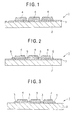
- FIG. 1 is a schematic sectional view showing an example of the first embodiment of the color filter according to the present invention.
- FIG. 2 is a schematic sectional view showing an another example of the first embodiment of the color filter according to the present invention.
- FIG. 3 is a schematic sectional view showing one example of the second embodiment of the color filter according to the present invention.
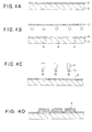
- FIG. 4 is a process drawing for explaining the third embodiment of a process for producing the color filter according to the present invention.
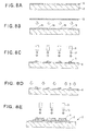
- FIG. 5 is a process drawing for explaining an another example of the third embodiment of a process for producing the color filter according to the present invention.
- FIG. 6 is a schematic plan view showing the first picture element part and the second picture element part in a process for producing showing in FIG. 5.
- FIG. 7 is a schematic plan view showing the examples of a photomask using in the process for producing the color filter according to the present invention.
- FIG. 8 is a process drawing for explaining an another example of the third embodiment of a process for producing the color filter according to the present invention.
- FIG. 9 is a process drawing for explaining the forth embodiment of a process for producing the color filter according to the present invention.
- the color filter according to the present invention comprises a transparent substrate, a picture element part in which a plurality of colors are provided in the predetermined pattern with an ink jet system on the transparent substrate, and a wettability-variable layer being capable of varying the wettability which is provided for forming the picture element part.
- the present invention has a wettability-variable layer in order to form a picture element part as described above. Therefore, since a picture element part can be easily formed by varying the wettability of a wettability-variable layer, a color filter having the high quality can be obtained at the low cost.
- "In order to form a picture element part” herein includes the meaning that a picture element part is positioned on a transparent substrate.
- the color filter according to the present invention having such the wettability-variable layer is explained in detail below by means of some embodiments.
- the first embodiment of the present invention is a color filter in which the picture element part is provided on the predetermined portion on the wettability-variable layer which is formed on the transparent substrate.
- a picture element part is provided on a wettability-variable layer being capable of varying the wettability in a color filter without a shading part. Therefore, the wettability of a part on which a picture element part is to be provided in advance can be made into an inkphilic region having the small contact angle with a liquid and the other part can be made into an ink-repellent region having the large contact angle with a liquid.
- an ink is adhered to only an inkphilic region having the small contact angle with a liquid by coloring the picture element part forming portion on which a picture element part is to be provided, with an inkjet system, in spite of a surface of a transparent substrate without a shading part, an ink is uniformly spread over the whole picture element part, and a region having no ink is not present and color nonuniformity and the like do not occur in a picture element part, and an ink is not adhered to the other ink-repellent region.
- FIG. 1 shows one example of a color filter of the present embodiment.
- This color filter 1 comprises a wettability-variable layer 3 formed on a transparent substrate 2, and a picture element part 4 having three color parts of red(R), green(G), and blue(B) formed on the wettability-variable layer 3.
- an protecting layer may be formed on the picture element part 4 as needed.
- a space between the picture element parts 4 is narrow. Since a color filter of the present embodiment is a type of color filter in which a black matrix (shading part) is not provided, when actually using for a liquid crystal display, it is necessary to use together with a back light side substrate having a black-matrix. In this case, when a space between the picture element parts is wide, it is necessary to have a high precision concerning positioning with the back light side substrate on which the black-matrix is provided. If it is not so, a back light penetrates the space between the picture element parts, as a result, the so-called color missing may occur so it is not preferable.
- a colored layer consisting of the picture element parts can be smoothness through that the space between the picture element parts is narrow like that.
- a disatnce between the picture element parts is not more than 2 ⁇ m, particularly, not more than 1 ⁇ m. If necessary, there may be no space between the picture element parts of the color filter in the present invention.
- FIG. 2 shows an another example of a color filter of the present embodiment.
- a color filter comprises a wettability-variable layer 3 formed on a transparent substrate 2, and a picture element part 4 formed on the wettability-variable layer 3. Further, an ink-repellent convex part 5 which has an ink-repellent property, is formed on a portion between the picture element parts 4.
- an ink-repellent convex part 5 is formed in a color filter 1 of this example like this, an ink is not flown out over this ink-repellent convex part 5 upon adhering an ink to a picture element part forming portion with an ink jet system and, thus, a color filter having a picture element part which does not mix with an ink of an another color can be obtained.
- the wettability-variable layer is not particularly limited so long as the wettability of the surface thereof can be varied by the external stimulation, for example, physical stimulation and chemical stimulation.
- the layer may be a layer in which the state of roughness of the surface is varied by an acid, an alkali and the like and, whereby, the wettability is varied, or a layer in which a substance in the wettability-variable layer is changed by irradiation of the energy such as the ultraviolet light, the visible light and the heat and, whereby, the wettability is changed.
- the layer may be a wettability-variable layer in which a contact angle with a liquid is great before the addition of stimulation and a contact angle with a liquid is changed so that it becomes smaller after the addition of stimulation, or a wettability-variable layer in which a contact angle with a liquid is conversely small before the addition of stimulation and a contact angle with a liquid is greatly changed.
- this wettability-variable layer is a photocatalyst-containing layer in which the wettability changes so that a contact angle with a liquid is reduced by the energy irradiation.
- the photocatalyst-containing layer in which the wettability changes so that a contact angle with a liquid is reduced by exposure (which means not only the light irradiation but also the energy irradiation in the present invention) like this, the photocatalyst-containing layer can be made into an inkphilic region having the small contact angle with a liquid by pattern-irradiating with the energy to easily change the wettability and, for example, only a part on which a picture element part is to be formed can be easily made into an inkphilic region. Therefore, a color filter can be manufactured effectively and it becomes advantageous in a respect of cost. In this case, it is preferable that the light including the ultraviolet ray is used as the energy.
- An inkphilic region herein is a region having the small contact angle with a liquid and is intended to refer to a region having the better wettability relative to an ink for an ink jet, a coating material for a shading part and the like.
- an ink-repellent region is a region having the great contact angle with a liquid and is intended to refer to a region having the worse wettability relative to an ink for an ink jet, a coating material for a shading part and the like.
- a contact angle with a liquid having the surface tension of 40 mN/m is 10 degrees or more in a part not exposed, preferably a contact angle with a liquid having the surface tension of 30 mN/m is 10 degrees or more and, particularly, a contact angle with a liquid having the surface tension of 20 mN/m is 10 degrees or more.
- the photocatalyst-containing layer is a layer in which a contact angle with a liquid is reduced when exposed and a contact angle with a liquid having the surface tension of 40 mN/m becomes less than 10 degrees, preferably a contact angle with a liquid having the surface tension of 50 mN/m becomes 10 degrees or less and, particularly, a contact angle with a liquid having the surface tension of 60 mN/m becomes 10 degrees or less.
- a contact angle with a liquid of an exposed part is high, there is a possibility that the spread of an ink or a coating material for a shading part in this part is inferior and color missing or the like occurs in a picture element part.
- a contact angle with a liquid herein is obtained from the results by measuring a contact angle with liquids having various surface tensions using a contact angle measuring apparatus (type CA-Z manufactured by Kyowa Interface science Co., Ltd.) (after 30 seconds from dropping a droplet from a microsyringe) or making a graph from the results.
- a contact angle measuring apparatus type CA-Z manufactured by Kyowa Interface science Co., Ltd.
- the wettability index standard solutions manufactured by Junsei Science Co., Ltd. can be used as liquids having various surface tensions upon this measurement.
- a photocatalyst-containing layer in the present invention comprises at least a photocatalyst and a binder.
- a carrier produced by the light irradiation has influences on the chemical structure of organic substances by the direct reaction with an adjacent compound or active oxygen species in the presence of oxygen and water.
- the layer can be made into inkphilic by changing the wettability of an exposed part using the action of oxidation, degradation and the like of an organic group which is a portion of a binder or additives with a photocatalyst and, whereby, there can be arisen the great difference in the wettability between an exposed part and an unexposed part.
- the acceptability inkphilicity
- the repellent properties ink-repellent properties
- the photocatalyst-containing layer may be formed such that it contains at least a photocatalyst and fluorine and further the content of fluorine in the surface of this photocatalyst-containing layer is reduced with the aforementioned action of a photocatalyst as compared with before the energy irradiation upon irradiating the photocatalyst-containing layer with the energy.
- a pattern comprising a part having the small content of fluorine can be easily formed by pattern-irradiating with the energy.
- fluorine has the extremely low surface energy and, for this reason, the surface of a substance having a large amount of fluorine becomes smaller in the critical surface tension. Therefore, the critical surface tension of a part containing a small amount of fluorine becomes greater as compared with the critical surface tension of the surface of a part containing a great amount of fluorine.
- a part containing a small amount of fluorine becomes an inkphilic region as compared with a part containing a great amount of fluorine.
- the formation of a pattern comprising a part having a small amount of fluorine as compared with the surrounding surface results in the formation of an inkphilic region pattern in an ink-repellent region.
- the content of fluorine in an inkphilic region having the lower content of fluorine which was formed by the energy irradiation is 10 or less, preferably 5 or less, particularly preferably 1 or less when the fluorine content in a part not irradiated with the energy is 100.
- Various methods which are generally performed can be used to measure the fluorine content in such the photocatalyst-containing layer and, for example, a method which can quantitatively measure the fluorine amount in the surface such as X-ray Photoelectron Spectroscopy, also called as ESCA (Electron Spectroscopy for Chemical Analysis), fluorescent X-ray analysis, and mass spectroscopy can be used, being not limiting.
- X-ray Photoelectron Spectroscopy also called as ESCA (Electron Spectroscopy for Chemical Analysis)
- fluorescent X-ray analysis and mass spectroscopy
- photocatalyst used in the present invention, mention may be made of photosemiconductors such as titanium oxide (TiO 2 ), zinc oxide (ZnO), tin oxide (SnO 2 ), strontium titanate (SrTiO 3 ), tungten oxide (WO 3 ), bismuth oxide (Bi 2 O 3 ), and iron oxide (Fe 2 O 3 ).
- photosemiconductors such as titanium oxide (TiO 2 ), zinc oxide (ZnO), tin oxide (SnO 2 ), strontium titanate (SrTiO 3 ), tungten oxide (WO 3 ), bismuth oxide (Bi 2 O 3 ), and iron oxide (Fe 2 O 3 ).
- photosemiconductors such as titanium oxide (TiO 2 ), zinc oxide (ZnO), tin oxide (SnO 2 ), strontium titanate (SrTiO 3 ), tungten oxide (WO 3 ), bismuth oxide (Bi 2 O 3 ), and
- titanium oxide is suitably used because titanium oxide has the high band gap energy, is chemically stable and not toxic, and can be obtained easily.
- titanium oxide has the high band gap energy, is chemically stable and not toxic, and can be obtained easily.
- anatase and rutile There are two types of titanium oxide, anatase and rutile. Although both can be used in the present invention, anatase-type titanium oxide is preferable.
- Anatase-type titanium oxide has the excitation wavelength of not greater than 380 nm.
- anatase-type titanium oxide mention may be made of hydrochloric acid-defloccuated-type anatase-type titania sol (STS-02 (average particle size 7 nm) manufactured by Ishihara Sangyo Kaisha, LTD., ST-K01 manufactured by Ishihara Sangyo Kaisha, LTD.), and nitric acid-defloccuated-type anatase-type titania sol (TA-15 (average particle size 12nm) manufactured by Nissan Chemical Industries, Ltd.).
- STS-02 hydrochloric acid-defloccuated-type anatase-type titania sol
- TA-15 average particle size 12nm
- the small particle size of a photocatalyst is preferable because the photocatalystic reaction occurs effectively.
- the average particle size of 50 nm or less is preferable and it is particularly preferable to use a photocatalyst having the average particle size of not greater than 20 nm.
- the particle size of a photocatalyst is smaller, the surface roughness of a photocatalyst-containing layer becomes smaller, being preferable.
- the particle size of a photocatalyst exceeds 100 nm, the central line average surface roughness becomes larger, the ink-repellent properties of an unexposed part of a photocatalyst-containing layer are reduced and manifestation of the inkphilic properties of an exposed part becomes insufficient, being not preferable.
- the color filter of the present invention may be a color filter obtained by incorporating fluorine in the surface of a photocatalyst-containing layer as described above, reducing the fluorine content in the surface of a photocatalyst-containing layer by pattern-irradiating the surface of this photocatalyst-containing layer with the energy and, thereby, forming the pattern of an inkphilic region in an ink-repellent region and forming a picture element part and the like thereon.
- titanium oxide is preferably used as a photocatalyst.
- the content of fluorine contained in a photocatalyst-containing layer when titanium oxide is used like this, is preferable such that fluorine (F) element is contained in the surface of a photocatalyst-containing layer at an amount of not less than 50, preferably not less than 800, particularly preferably 1200 relative to 100 of titanium (Ti) element as quantitatively determined by analyzing by X-ray photoelectron spectroscopy.
- the fluorine content in an inkphilic region formed by the pattern irradiation of the energy is such that fluorine (F) element is contained at a rate of not greater than 50, preferably not greater than 20, particularly preferably not greater than 10 relative to 100 of titanium (Ti) element.
- the fluorine content in a photocatalyst-containing layer can be reduced to such the degree, the sufficient inkphilic properties can be obtained in order to form a picture element part and the like, it becomes possible to form a picture element part and the like with the better precision due to the difference in the wettability between the inkphilic region and the ink-repellent region not irradiated with the energy, and a color filter having the better quality can be obtained.
- a binder used in a photocatalyst-containing layer has such the high binding energy that the principal chain is not degraded by the photoexcitation of the aforementioned photocatalyst, for example, mention may be made of (1) organopolysiloxane which exerts the great strength and which is obtained by hydrolyzing and polymerization-condensing chloro or alkoxysilane by a sol-gel reaction or the like, and (2) organopolysiloxane obtained by cross-linking reactive silicone having the excellent water-repellency and oil-repellency.
- organopolysiloxane which is obtained by hydrolyzing and condensing or cohydrolyzing and condensing one or more of silicon compounds represented by the general formula: Y n SiX (4-n) (wherein Y represents alkyl group, fluoroalkyl group, vinyl group, amino group, phenyl group or epoxy group, X represents alkoxyl group, acetyl group or halogen, and n is an integer of 0 to 3).
- a number of carbon of a group denoted by Y is preferably in a range of 1 to 20 and alkoxyl group denoted by X is preferably methoxy group, ethoxy group, propoxy group, and butoxy group.
- polysiloxane containing fluoroalkyl group can be preferably used. More particularly, mention may be made of hydrolyzed and condensed compound and cohydrolyzed and condensed compound of one or more of the following fluoroalkylsilanes. Generally, the known fluorine-contained silane coupling agents can be used.
- polysiloxane containing aforementioned fluoroalkyl group is used as a binder, the ink-repellent properties in a photocatalyst-containing layer are remarkably improved and the function of preventing a coating material for a shading part or an ink for an ink jet system from adhering is manifested.
- n is an integer of not smaller than 2
- R 1 and R 2 are each substituted or unsubstituted alkyl, alkenyl, aryl or cyanoalkyl group having 1-10 carbon numbers, respectively, and not greater than 40% of the whole in moles is vinyl, phenyl or halogenated phenyl.
- the compounds wherein R 1 and R 2 are methyl group are preferable because the surface energy becomes the smallest. Am amount of not smaller than 60% in terms of a mole rate of methyl group is preferable.
- a molecular chain has at least one reactive group such as hydroxy group at an end of a chain and a side chain.
- an stable organosilicon compound which does not perform a cross-linking reaction such as dimethylpolysiloxane may be mixed into a binder together with the aforementioned organopolysilicon.
- various binders such as organopolysiloxane and the like can be used in a photocatalyst-containing layer like this.
- fluorine in the surface of a photocatalyst-containing layer may be reduced and, thereby, an inkphilic region may be formed within an ink-repellent region by incorporating fluorine in a photocatalyst-containing layer containing such the binder and the photocatalyst and pattern-irradiating with the energy.
- fluorine needs to be contained in a photocatalyst-containing layer and, as a method of incorporating fluorine into such the photocatalyst-containing layer containing a binder, mention may be made of a method of binding a fluorine compound with a binder which usually have the high binding energy, using the relatively weak binding energy, and a method of mixing into a photocatalyst-containing layer a fluorine compound which is bound by the relatively weak binding energy.
- a fluorine-bound site having the relatively small binding energy is first degraded and, thereby, fluorine can be removed from a photocatalyst-containing layer.
- the aforementioned first method that is, a method of binding a fluorine compound with a binder which have the high binding energy using the relatively weak binding energy
- organopolysiloxane which exerts the great strength can be obtained by hydrolyzing and polymerization condensing chloro or alkoxysilane and the like by a sol-gel reaction, which is described as (1).
- organopolysiloxane is obtained by hydrolyzing and condensing or cohydrolyzing and condensing one or more of silicon compounds represented by the general formula: Y n SiX (4-n) (wherein Y represents alkyl group, fluoroalkyl group, vinyl group, amino group, phenyl group or epoxy group, X represents alkoxyl group, acetyl group or halogen, and n is an integer of 0 to 3) as described above.
- Y represents alkyl group, fluoroalkyl group, vinyl group, amino group, phenyl group or epoxy group
- X represents alkoxyl group, acetyl group or halogen
- n is an integer of 0 to 3
- organopolysiloxane having a fluoroalkyl group as a substituent group is used as a binder, since a part of a carbon-carbon bond of a fluoroalkyl group is degraded by the action of a photocatalyst in a photocatalyst-containing layer upon the energy irradiation, the fluorine content of a part of the surface of a photocatalyst-containing layer irradiated with the energy can be reduced.
- a silicon compound having a fluoroalkyl group using upon this a silicon compound having at least one fluoroalkyl group and in which a number of a carbon element in this fluoroalkyl group is 4 to 30, preferably 6 to 20, particularly preferably 6 to 16 is suitably used, being not limiting. Specific examples of such the silicon compound are described as above and, inter alia, the silicon compound having a fluoroalkyl group in which a number of carbon element is 6 to 8 is preferable.
- such the silicon compound having a fluoroalkyl group may by used by mix with a silicon compound having no fluoroalkyl group as described above, and a co-hydrolyzed and condensed compound of which may be used as the organopolysiloxane.
- a silicon compound having no fluoroalkyl group as described above
- a co-hydrolyzed and condensed compound of which may be used as the organopolysiloxane.
- one or more of such the silicon compounds having the fluoroalkyl group may be used, and a hydrolyzed and condensed compound or a co-hydrolyzed and condensed compound of which may be used as the organopolysiloxane.
- organopolysiloxane having a fluoroalkyl group thus obtained, it is preferable that, among silicon compounds constituting this organopolysiloxane, the silicon compound having a fluoroalkyl group is contained at an amount of not less than 0.01 mol%, preferably not less than 0.1 mol%.
- the ink-repellent properties on a photocatalyst-containing layer can be enhanced and the difference in the wettability between a part of an ink-repellent region and a part which was converted into an inkphilic region by the energy irradiation can be made to be larger.
- organopolysiloxane is obtained by cross-linking a reactive silicone having the excellent water-repellency and oil-repellency.
- a substituent containing fluorine such as fluoroalkyl group and the like as either R 1 or R 2 in the above general formula or both, fluorine can be contained in a photocatalyst-containing layer.
- fluorine content in the surface of a photocatalyst-containing layer can be reduced by the energy irradiation.
- a method of introducing a fluorine compound which is bound by the weaker energy than the binding energy of a binder mention may be made of a method of mixing a fluorine-contained surfactant therein when a fluorine compound having a low molecular weight is introduced and, as a method of introducing a fluorine compound having a high molecular weight, mention may be made of a method of mixing a fluorine-contained resin having the high compatibility with a binder resin.
- a photocatalyst-containing layer may contain a surfactant besides the aforementioned photocatalyst and binder. More particularly, mention may be made of a hydrocarbon nonionic surfactant such as NIKKOL BL, BC, BO, BB series manufactured by Nikko Chemicals Co., ltd., and a fluorine-contained or silicone-contained nonionic surfactant such as ZONYL FSN, FSO manufactured by Dupont Co., Ltd., Surfron S-141 and 145 manufactured by Asahi Glass Co., Ltd., Megafack F-141 and 144 manufactured by Dainippon Ink & Chemicals Co., Ltd., Ftagent F-200 and F251 manufactured by Neos Co., Ltd., Unidyne DS-401 and 402 manufactured by Daikin Industries, Ltd., Florad FC-170 and 176 manufactured by 3M Co., Ltd.
- a surfactant besides the aforementioned photocatalyst
- a photocatalyst-containing layer may contain an oligomer and a polymer such as polyvinylalcohol, unsaturated polyester, acrylic resin, polyethylene, diallyl phthalate, ethylene propylene diene monomer, epoxy resin, phenol resin, polyurethane, melamine resin, polycarbonate, polyvinyl chloride, polyamide, polyimide, styrene butadiene rubber, chloroprene rubber, polypropylene, polybutylene, polystyrene, polyvinyl acetate, polyester, polybutadiene, polybenzimidazole, polyacrylnitrile, epichlorhydrin, polysulfide, polyisoprene, and the like in addition to the aforementioned surfactants.
- a polymer such as polyvinylalcohol, unsaturated polyester, acrylic resin, polyethylene, diallyl phthalate, ethylene propylene diene monomer, epoxy resin, phenol resin, polyurethane, mel
- the content of a photocatalyst in a photocatalyst-containing layer can be set in a range of 5 to 60% by weight, preferably 20 to 40% by weight.
- the thickness of a photocatalyst-containing layer is preferably in a range of 0.05 to 10 ⁇ m.
- the aforementioned photocatalyst-containing layer can be formed by dispersing a photocatalyst and a binder and, if needed, other additives in a solvent to prepare a coating solution, and applying this coating solution.
- a solvent used an alcoholic organic solvent such as ethanol, isopropanol and the like is preferable. Applying can be performed by the known applying method such as spin coating, spray coating, dip coating, roll coating, bead coating or the like.
- an ultraviolet-curing type binder is contained as a binder
- a photocatalyst-containing layer can be formed by performing the curing treatment by the ultraviolet ray irradiation.
- a picture element part 4 is provided on a wettability-variable layer 3, inter alia, the aforementioned photocatalyst-containing layer as shown in FIG. 1 and FIG. 2.
- a picture element part is formed in an inkphilic region which is formed by exposing the aforementioned photocatalyst-containing layer, having the low contact angle with a liquid in the predetermined pattern by a plurality of colors of inks with an ink jet system.
- a picture element part is usually formed of three colors of red (R), green (G) and blue (B). The coloring pattern and an area to be colored in this picture element part can be set arbitrarily.
- a shading part (a black matrix) does not exist between picture element parts. Therefore, two cases can be found, one of which is the case in which a space exist between picture element parts, and another of which is the case in which a picture element part is formed continuously. In the present embodiment, either one may be acceptable. Further, as showing in FIG. 2, it is acceptable that an ink-repellent convex part is provided.
- Inks for an ink jet system for forming such the picture element part are roughly divided into an aqueous ink and an oil based ink.
- an aqueous ink based on water is preferable in a respect of the surface tension.
- Water alone or a mixed solvent of water and a water-soluble organic solvent can be used as a solvent for an aqueous ink used in the present invention.
- an ink based on a solvent having a high boiling point is preferably used for an oil based ink in order to prevent the choking of a head.
- a coloring agent used for such the ink for an ink jet system the known pigments and dyes are widely used.
- insoluble or soluble resins may be contained in a solvent in order to improve the dispersibility and the fixing properties.
- surfactant containing nonionic surfactant, cationic surfactant and amphoteric surfactant may be added thereto as the occasion demands.
- the conventional ink for an ink jet system can not contain a large amount of a binder resin due to the low suitable viscosity, it is possible to impart the fixing ability to a coloring agent itself by granulating so as to wrap a coloring agent particle with a resin in an ink.
- Such the ink can be also used in the present invention.
- so-called hot melt ink and UV-curing ink may be used.
- an UV-curing ink is preferably used.
- a picture element part is formed by coloring with an ink jet system and, thereafter, UV is irradiated and, thereby, an ink can be cured rapidly which can sent to a next step immediately. Therefore, a color filter can be manufactured effectively.
- Such the UV-curing ink has a prepolymer, a monomer, a photopolymerization initiator and a coloring agent as a main component.
- a prepolymer any prepolymer such as polyesteracrylate, polyurethaneacrylate, eposyacrylate, polyetheracrylate, oligoacrylate, alkydacrylate, polyolacrylate, siliconacrylate and the like can be used without limitation.
- vinyl monomer such as styrene, vinyl acetate and the like; monofunctional acrylic monomer such as n-hexylacrylate and phenoxyethylacrylate; and multifunctional acrylic monomer such as diethylene glycol diacrylate, 1,6-hexanediol diacrylate, hydroxypiperic ester neopentylglycol diacrylate, trimethylolpropane triacrylate, dipentaerhythritolhexane acrylate and the like can be used.
- the aforementioned prepolymers and monomers may be used alone or in a mixture of two or more of them.
- an initiator which imparts the desired curing properties and the desired recording properties can be selected for use among isobutylbenzoin ether, isopropylbenzoin ether, benzoin ethyl ether, benzoin methyl ether, 1-phenyl-1,2-propadione-2-oxime, 2,2-dimethoxy-2-phenylacetophenone, benzil, hydroxycyclohexyl phenyl ketone, diethoxyacetophenone, 2-hydroxy-2-methyl-1-phenylpropane-1-one, benzophenone, chlorothioxanthone, 2-chlorothioxanthone, isopropylthioxanthone, 2-methylthioxanthone, chlorine-substituted benzophenone, halogen-substituted alkyl-allylketone and the like.
- Other components such as photoinitiator assistant such as aliphatic amine, aromatic amine and the like;
- the wettability-variable layer 3 inter alia, the aforementioned photocatalyst-containing layer is provided on a transparent substrate 2 as shown in FIG. 1 and FIG. 2.
- substrates which have hitherto been used for a color filter can be used, without limitation, such as a transparent rigid material having no flexibility such as quartz glass, Pyrex glass, synthetic quartz glass and the like, or a transparent flexible material having the flexibility such as a transparent resin film, a resin plate for optics and the like.
- a transparent rigid material having no flexibility such as quartz glass, Pyrex glass, synthetic quartz glass and the like
- a transparent flexible material having the flexibility such as a transparent resin film, a resin plate for optics and the like.
- 7059 glass manufactured by Corning Co., Ltd. is a material having the small thermal expansion coefficient and is excellent in the dimensional stability and the workability at heat-treatment at an elevated temperature and, additionally, since it is non-alkali glass containing no alkaline component in a glass, it is suitable for a color filter for a color liquid crystal display apparatus by an active matrix system.
- a transparent material is usually used for a transparent substrate and a reflective substrate and white-colored substrate may be used.
- a transparent substrate substrates having the surface treated for preventing the alkali dissolution or for imparting the gas barrier properties or for other objects may be used.
- an ink-repellent convex part 5 may be formed between picture element parts 4 as shown in FIG. 2.
- the composition of such the ink-repellent convex part is not particularly limited as long as it is a resin composition having the ink-repellent properties.
- the composition is not necessarily transparent and may be colored.
- a material which is used for a black matrix (shading part) and which is a material with no black material incorporated therein can be used.
- a composition of a water soluble resin such as polyacrylamide, polyvinyl alcohol, gelatin, casein, cellulose and the like alone or a mixture of two or more of them, and a resin composition such as O/W emulsion, for example, an emulsified reactive silicone.
- a photocuring resin is suitable used for the reasons of easy handling and curing.
- this ink-repellent convex part is preferable as it grows ink-repellent, the surface thereof may be treated with an ink-repellent treating agent such as a silicone compound and a fluorine-containing compound.
- An ink-repellent convex part in the aforementioned first embodiment is preferably relatively higher because it is provided for preventing an ink from mixing upon coloring with an ink jet system but, in view of the flatness of the whole when it is made into a color filter, the thickness near that of a picture element part is preferable. More particularly, it is usually preferably in a range of 0.1 to 2 ⁇ m although it is different depending upon an accumulated amount of an ink blown.
- a protecting layer may be further formed on a surface of a color filter 1 as the occasion demands though not shown in FIG. 1 or FIG. 2.
- This protecting layer is provided for flattening a color filter and at the same time preventing components contained in a picture element part, or a picture element part and a photocatalyst-containing layer from dissolving into a liquid crystal layer.
- the thickness of a protecting layer can be set in view of the light transmittance of a material used, the surface condition of a color filter and the like and, for example, it can be set in a range of 0.1 to 2.0 ⁇ m.
- a protecting layer can be formed using a resin having the light transmittance required for a transparent protecting layer among the known transparent photosensitive resin, two-pack curing type transparent resin and the like.
- the second embodiment of the present invention is a color filter in which a picture element part is formed on a transparent substrate, and the wettability-variable layer is formed on a boundary portion of the picture element parts.
- FIG. 3 shows one example of the second embodiment.
- This color filter 1 is formed of a transparent substrate 2, a picture element part 4 formed on the transparent substrate 2, and a wettability-variable layer 3 formed between the picture element parts 4.
- a protecting layer not shown in the drawings may be provided on the picture element part 4 and the wettability-variable layer 3 as the occasion demands.
- the characteristics of this embodiment are in that a wettability-variable layer 3 is provided on only a boundary portion of a picture element part 4 on a transparent substrate 2 and a picture element part 4 is formed on the transparent substrate 2 directly. Since, in the second embodiment, a wettability-variable layer 3 is formed on only a boundary portion of a picture element part 4 like this, when the wettability is changed by adding the stimulation to a wettability-variable layer 3, the stimulation may be added over the whole side and the stimulation does not necessarily be added in a pattern like state. Therefore, there are effects that steps after formation of a wettability-variable layer may be simplified.
- a surface of a transparent substrate 2 is inkphilic.
- a surface of a transparent substrate 2 is an inkphilic region compared with a wettability-variable layer 3 which is an ink-repellent region before the change in the wettability in view of formation of a picture element part 4.
- the wettability on a transparent substrate 2 is less than 10 degrees as the contact angle with a liquid having the surface tension of 40 mN/m, more preferably not more than 5 degrees, particularly preferably not more than 1 degree.
- a transparent substrate As a transparent substrate, the surface of which is an inkphilic region, there are a substrate formed of an inkphilic material, a substrate obtained by treating the surface of a material so as to make the surface inkphilic, and an inkphilic layer is formed on a transparent surface, being not limiting in this embodiment.
- the inkphilic surface treatment with the plasma treatment utilizing argon and water
- the third embodiment of the present invention is a process for producing a color filter which is the aforementioned first embodiment in the present invention, and said process comprises;
- FIG. 4 is for explaining each step of the third embodiment of the present invention.
- a photocatalyst-containing layer 6 is formed on a transparent substrate 2.
- This photocatalyst-containing layer 6 is formed by dispersing the aforementioned photocatalyst and binder in a solvent, if necessary, together with other additives to prepare a coating solution, applying this coating solution, and proceeding the hydrolyzing and polymerization condensing reaction to fix firm a photocatalyst in a binder.
- alcoholic organic solvents such as ethanol, isopropyl alcohol and the like are preferable, and applying can be performed by the known applying method such as spin coating, spray coating, dip coating, roll coating, bead coating or the like.
- an exposed part for a picture element part 8 is formed on a picture element part forming portion on a photocatalyst-containing layer 6 through pattern-irradiated with the energy using a photomask 7.
- the exposed part for a picture element part 8 is a portion on which the contact angle with a liquid is lowered by the action of a photocatalyst which is included in a photocatalyst-containing layer 6, and converted into an inkphilic region (FIG. 4 (B)).
- an ink 10 is injected into an exposed part for a picture element part 8, which was converted into an inkphilic region by the energy irradiation, to color the part with red, green and blue (FIG. 4 (C)).
- an ink 10 injected from an ink jet apparatus 9 is spread uniformly in an exposed part for a picture element part 8.
- An ink jet apparatus used in the present invention is not particularly limited but an ink jet apparatus can be used which uses various methods such as a method of injecting a charged ink continuously and controlling with the magnetic field, a method of injecting an ink intermittently using a piezo-element, a method of injecting an ink intermittently by heating the ink and utilizing its bubbling.
- a picture element part 6 is formed by solidifying the ink thus adhered to an exposed part for a picture element part 12 (FIG. 4 (D)).
- the solidification of an ink is carried out by various methods depending upon a kind of an ink used. For example, in the case of a water-soluble ink, the solidification is performed by removing water by heating or the like.
- an ink is preferably a UV-curing ink. This is because since a UV-curing ink can be rapidly solidified by the UV irradiation, a time for producing a color filer can be shortened.
- a picture element part 4 can be formed through irradiating with energy at a time and adhering ink to an exposed part.
- adhering ink there is a narrow space between exposed parts for an picture element part which is an inkphilic region irradiated with energy. Therefore, there are some possibilities to occur some problems such as mixing two sorts of ink for adjacent picture element parts during formation of the picture element part.
- a method shown in FIG.5 may be proposed, in which a step of irradiating with energy and forming a picture element part are divided into at least two times.
- a photocatalyst-containing layer 6 is formed on a transparent substrate 2, similar to that of the third embodiment described above (FIG. 5 (A)).
- the energy is irradiated using a photomask similar to the above-described method.
- the photomask is designed such that exposed parts for a picture element part correspond to the entire picture element part, can be formed.
- a photomask 7' is designed such that a picture element part can be formed alternately, then, a exposed part for the first picture element part 11 is formed on the photocatalyst-containing layer 6 using the photomask 7' (FIG.5 (B)).
- the ink 10 is injected to the exposed part for the first picture element part 11 converted into an inkphilic region by the energy irradiation to color, then cured to form the first picture element part 12 (FIG.5 (C)).
- the energy irradiation and coloring to a picture element part using inkjet apparatus are conducted similar to that of the first method except a shape of a photomask 7'.
- the first picture element part 12 formed by above-described method preferably has ink-repellent property itself in order to prevent the first picture element part from coloring by second ink injection through the inkjet apparatus. Further, the surface of the first picture element part can be treated with ink-repellent treatment agent such as silicone compounds or fluorine including compounds.
- the transparent substrate 2 on which the first picture element part 12 is formed is shown in FIG. 6 (A).
- the first red picture element part (R1) is formed, then the first blue picture element part (B1) is formed through skipping the first blue picture element part (G1).
- the second green picture element part (G2) is formed through skipping the second red picture element part (R2).
- the first picture element part 12 is formed alternately.
- An example of the photomask 7 using this step, is shown in FIG.7 as (A-1) or (B-1).
- the energy is again irradiated on the entire surface of the photocatalyst-containing layer 6 on which the first picture element part 12 is formed.
- the energy may be pattern-irradiated using a photomask again as well as the energy may be irradiated the entire surface like this.
- the photomask for second pattern-irradiating with the energy is designed such that an exposed part for the second picture element part 13 is formed between the first picture element parts 12, and it is possible to use the photomask, for example, shown in FIG.7 as (A-2) or (b-2).
- the portion except for an exposed part for the first picture element part 11 is also irradiated with the energy through the energy irradiation to an entire surface, to be converted to an inkphilic region (FIG.5 (D)).
- the ink 10 is injected to the inkphilic region through using a inkjet apparatus 9 for coloring the region, and cured the ink to form the second picture element part 14.
- the second picture element part 14 is illustrated in the figure such that there is a space between the second picture element parts 14 and the first picture element part, however, in practice, the second picture element part 14 is formed so as to fill up a space between the first picture element parts 12. Exposing and coloring to a picture element part using an inkjet apparatus are conducted similar to that of the example described above.
- FIG.6 (B) is shown the condition that the second picture element part is formed like this.
- the second picture element part 14 Through forming the second picture element part 14 so as to fill up a space between the first picture element parts 12, picture element parts having three color parts which sequences in order of red(R), green(G), and blue(B) from left side.
- a protecting layer is formed on the picture element part to form a color filter. Following is the reason why the formation of the picture element part is divided into two times.
- a shading part can not use as a partition. Therefore, when a picture element part is formed such that an exposed part for a picture element part converted to an inkphilic region through the energy irradiation, is colored by an inkjet system, and when a space between the exposed parts for a picture element part is narrow, that is, the width of an ink-repellent region where not irradiating with the energy is narrow, there are some possibilities of mixing some sorts of ink for adjacent picture element parts through migration over an ink-repellent region during formation of a picture element part. Accordingly, it is desirable to form adjacent picture element parts as apart as possible when forming the picture element part.
- the energy is pattern-irradiated such that the picture element part is formed alternately. Accordingly, the adjacent picture element part that is formed in the first time can be positioned apart.
- an exposed part for the first picture element part 11 can be formed in the condition that a relatively wide ink-repellent region exists between them. Therefore, there is no possibility of mixing some sorts of ink 10 for adjacent picture element parts when coloring through using an inkjet apparatus 9. Then, through irradiating again with the energy between the first picture element parts 12 by the entire irradiation or pattern-irradiation, a space between them are converted to an inkphilic region. And through coloring the space with an inkjet apparatus 9, a color filter which do not have disadvantage such as ink mixing and color nonuniformity, can be obtained.
- this method it is possible to reduce or eliminate a space between picture element parts. Therefore, a colored layer (aggregate of picture element parts) having the excellent flatness can be formed. When it is necessary to form a picture element part continuously, this method should be used.
- a photomask using when the second energy irradiation is pattern-irradiation may be a photomask shown in FIG.7 as (B-2), in which the entire region on which the first picture element is formed, is exposed to convert the entire ink-repellent region between the first picture element parts 12 to inkphilic region, or may be a photomask shown in FIG.7 as (A-2), in which the predetermined portion between the first picture element parts is exposed to form the second picture element part.
- a picture element part 6 was formed every other one first time, the present invention is not limited thereto but the change may be performed by the shape of a picture element part of a color filter such as zigzag-like or the like so long as the first formed picture element parts are not in the vicinity.
- a picture element part was formed by dividing into two times but a picture element part may be formed by dividing into three times or more.
- an ink-repellent convex part may be formed before forming a picture element part.
- the ink-repellent convex part is formed surrounding a picture element part region where the all picture element parts are to be formed, it can be prevented from a problem such that a picture element part can not be formed precisely because ink is flowed out at a portion surrounding a picture element part region.
- Such an ink-repellent convex part may be formed following steps; forming an exposed part for an ink-repellent convex part before forming an exposed part for a picture element part, and forming an ink-repellent convex part through applying a resin composition to the exposed part for an ink-repellent convex part.
- the photomask for forming the ink-repellent convex part described above may be employed one, for example, shown in FIG.7 as (C-1) or (D-1).
- an exposed part for an ink-repellent convex part is formed through using such a photomask and exposing on a photocatalyst-containing layer.
- the exposed part for an ink-repellent convex part is formed at the upper end side and at the lower end side of the picture element part region.
- the exposed part for an ink-repellent convex part is formed surrounding the picture element part region. Then, a resin composition is adhered to the exposed part for an ink-repellent convex part and cured to form an ink-repellent convex part.
- the first picture element part is formed through using the photomask shown in FIG.7 as (C-2) or (D-2), and then the second picture element part is formed through using the photomask shown as (A-2) or (B-2), or irradiating the entire surface), a picture element part is formed, and a color filter is formed.
- a region where the ink-repellent convex part may be formed between picture element parts as well as formed at upper and lower end part of a picture element part region or surrounding a picture element part region.
- FIG. 8 A step of forming this ink-repellent convex part will be explained using FIG. 8.
- a photocatalyst-containing layer 6 is formed so as to cover a transparent substrate 2 (FIG. 8 (A)), and thus obtained member is irradiated with the energy via a photomask for an ink-repellent convex part 15.
- an exposed part for an ink-repellent convex part 16 is formed on a photocatalyst-containing layer 6 on a boundary portion of a picture element part (FIG. 8 (B)).
- Ink for an ink-repellent convex part 17 such as a UV-curing resin monomer is adhered to this exposed part for an ink-repellent convex part 16 by an ink jet apparatus 9 (FIG. 8 (C)).
- a method of applying the ink for an ink-repellent convex part is not limited to a method by an ink jet apparatus but other methods, for example, dip coating and the like may be used.
- an ink-repellent convex part 5 is formed on the surface of a photocatalyst-containing layer 6 (FIG. 8 (C)).
- an exposed part for an ink-repellent convex part is provided by pattern-irradiating a photocatalyst-containing layer between picture element parts with the energy, an ink-repellent convex part having an arbitrary width can be formed. Therefore, by applying an ink for an ink-repellent convex part thereon, an ink-repellent convex part having an arbitrary width can be formed. Hence, by adjusting the width of a photomask for an ink-repellent convex part 15, adjusting the width between picture element parts can be conducted.
- an ink-repellent convex part is formed by utilizing the change in the wettability of a photocatalyst-containing layer but the formation is not limited to this in the present invention and, for example, an ink-repellent convex part may be provided by a photolithography or the like.
- the light including the ultraviolet light may be used as the energy to be irradiated to a photocatalyst-containing layer.
- a light source including the ultraviolet light for example, mention may be made of a mercury lamp, a metal halide lamp, a xenon lamp and the like.
- the wavelength of the light used for this exposure can be set from a range of not greater than 400 nm, preferably not greater than 380 nm.
- an amount of the light to be irradiated upon exposure may be an amount of irradiation necessary for an exposed part to express the inkphilic properties by the action of a photocatalyst.
- pattern-irradiation When pattern-irradiation is necessary upon the energy irradiation, pattern-irradiation can be performed via a photomask using the aforementioned light source.
- a method of picture-irradiating in a pattern like state using a laser such as excimer, YAG and the like.
- a laser such as excimer, YAG and the like.
- the pattern of an inkphilic region may be formed by adding the photocatalystic reaction initiating energy to a photocatalyst-containing layer, and adding the reaction rate increasing energy to a region which received the photocatalystic reaction initiating energy in a pattern like state.
- the reaction rate increasing energy such as the infrared laser which is relatively low cost and easily handled, can be used and the aforementioned problem does not occur.
- the pattern of an inkphilic region having the changed wettability can be formed by the addition of such the energy based on the following reasons. That is, first, by adding the photocatalystic reaction initiating energy to a region on which the pattern is to be formed, the photocatalystic reaction is initiated on a photocatalyst-containing layer. Then, the reaction rate increasing energy is added in a region which receives the photocatalystic reaction initiating energy. By adding the reaction rate increasing energy like this, a reaction in a photocatalyst-containing layer to which the photocatalystic reaction initiating energy has been already added and in which a reaction has been initiated by the catalytic action of a photocatalyst is rapidly accelerated.
- the change of the wettability in the photocatalyst-containing layer is changed into the desired range and, thus, the pattern to which the reaction rate increasing energy has been added can be made into the pattern of an inkphilic region having the changed wettability.
- the photocatalystic reaction initiating energy used for this energy irradiating method refers to the energy that a photocatalyst initiates a catalytic reaction for changing the properties of a compound in a photocatalyst-containing layer.
- An amount of the photocatalystic reaction irradiating energy to be added is such the degree of an amount that does not cause the rapid change in the wettability in a photocatalyst-containing layer.
- an amount of the photocatalystic reaction initiating energy to be added is small, since the sensitivity upon formation of the pattern by adding the reaction rate increasing energy is lowered, being not preferable.
- this amount is too large, the degree of the change in the properties in a photocatalyst-containing layer to which the photocatalystic reaction initiating energy has been added becomes too large and the difference between regions to which the reaction rate increasing energy has been added and not added becomes unclear, being not preferable.
- An amount of the energy to be added is determined by performing a preliminary experiment on an amount of the energy to be added and the change in the wettability in a photocatalyst-containing layer.
- the photocatalystic reaction initiating energy in this method is not particularly limited as long as the energy which can initiate the photocatalystic reaction and, inter alia, the light is preferable.
- a photocatalyst used in the present invention has the different wavelength of the light, which initiates a catalytic reaction depending upon the band gap thereof.
- the wavelength is 496 nm and, in the case of iron oxide, the wavelength is 593 nm of the visible light and, in the case of titanium oxide, the wavelength is 388 nm of the ultraviolet light. Therefore, the light can be used in the present invention whether the visible light or the ultraviolet light as long as the light.
- the light is preferably the light containing the ultraviolet light which initiates a catalytic reaction of this titanium oxide. More particularly, it is preferable that the ultraviolet light in a range of not greater than 400 nm, preferably not greater than 380 nm is contained.
- the light source for such the light containing the ultraviolet light mention may be made of various ultraviolet sources such as a mercury lamp, a metal halide lamp, a xenon lamp, an excimer lamp and the like.
- a range to which this photocatalystic reaction initiating energy is to be added may be a part of a photocatalyst-containing layer.
- this photocatalystic reaction initiating energy in a pattern like state and further adding the reaction rate increasing energy also in a pattern like state, it is possible to form the pattern of an inkphilic region having the changed wettability.
- this photocatalystic reaction initiating energy is added to the whole surface of a region on which the pattern is to be formed.
- the reaction rate increasing energy to a region to the whole surface of which the photocatalystic reaction initiating energy has been added in a pattern like state, the pattern of an inkphilic region is formed on a photocatalystic-containing layer.
- the reaction rate increasing energy used in this method refers to the energy for increasing a reaction rate of a reaction changing the wettability of a photocatalyst-containing layer which was initiated by the aforementioned photocatalystic reaction initiating energy.
- any energy can be used as long as it is the energy having such the action and, inter alia, the heat energy is preferably used.
- a method of adding such the heat energy to a photocatalyst-containing layer in a pattern like state is not particularly limited as long as it can form the pattern by the heat on a photocatalyst-containing layer but mention may be made of a method by the infrared laser, a method by a heat-sensitive head and the like.
- the infrared laser mention may be made of the infrared YAG laser (1064 nm) having the advantages such as the strong directivity and the long irradiation distance, a diode laser (LED; 830 nm, 1064 nm, 1100 nm) having the advantages such as the relatively low cost, a semiconductor laser, a He-Ne laser, a carbonic dioxide gas laser and the like.
- the pattern of an inkphilic region can be formed based on the difference in the reaction rate between regions to which the reaction rate increasing energy has been added and a region to which the reaction rate increasing energy has not been added, by adding the aforementioned photocatalystic reaction initiating energy and activating a photocatalyst to initiate the change in the wettability by the catalytic reaction in a photocatalyst-containing layer, and adding the reaction rate increasing energy to a part having the changed wettability to promote the catalytic reaction of the part.
- the forth embodiment of the present invention is one of processes for producing a color filter of the aforementioned second embodiment of the present invention, and comprises:
- a photocatalyst-containing layer 6 is first formed on a boundary portion of a picture element part forming portion, on which a picture element part is to be formed, on a transparent substrate 2.
- a method of forming a photocatalyst-containing layer in a pattern like state for example, mention may be made of a method forming the layer by a photolithography using a photosensitive sol-gel solution, a method by printing and the like.
- Ink 10 is adhered using an ink jet apparatus 9 on a part (picture element part forming portion) on which a photocatalyst-containing layer 6 is not formed, on a transparent substrate 2 on which the thus formed photocatalyst-containing layer 6 is formed (FIG. 9 (B)).
- the wettability of the surface of a transparent substrate 2 has been made into more inkphilic as compared with the wettability of a surface on a photocatalyst-containing layer 6.
- ink 10 upon formation of a picture element part 4, ink 10 is not adhered to a photocatalyst-containing layer showing the ink-repellent properties and is adhered to only a picture element part forming portion on a transparent substrate 2, to form a picture element part. Then, adhered ink is cured to form a picture element part 4 between a photocatalyst-containing layer 6 (FIG. 9 (C)).
- a protecting layer (not shown in a drawing) which is formed as needed, can be formed easily because a photocatalyst-containing layer 6 is converted into an inkphilic region.
- the wettability on a transparent substrate 2 is inkphilic. More particularly, it is preferable that the wettability is less than 10 degrees as the contact angle with a liquid having the surface tension of 40 mN/m, more preferably not more than 5 degrees as the contact angle with a liquid having the surface tension of 40 mN/m, particularly preferably not more than 1 degree. This is because, by making a surface of a transparent substrate 2 into an inkphilic region, an ink 10 is uniformly spread over a transparent substrate and disadvantages such as color nonuniformity and the like do not occur.
- a color liquid crystal panel can be formed by combining the thus obtained color filter, and an opposite substrate which is opposite to this color filter and having a black matrix, and encapsulating a liquid crystal compound therebetween.
- the thus obtained color liquid crystal panel has the advantages originated from the color filter of the present invention, that is, advantages that color nonuniformity and color missing do not occur, and it is advantageous in a respect of cost.
- the present invention is not limited to the aforementioned embodiments.
- the aforementioned embodiments are merely illustrative and whatsoever has the substantially same construction as that described in claims and exerts the same action and effects are included in the present invention.
- composition was applied on a glass transparent substrate with a spin coater and dried at 50 °C for 10 minutes to form a transparent photocatalyst-containing layer (thickness 0.2 ⁇ m).
- the pattern-exposure was performed for 50 seconds on this photocatalyst-containing layer at an illuminance of 70 mW/cm 2 with a mercury lamp (wavelength 365 nm) via a photomask, an exposed part was formed and the contact angles with a liquid of an unexposed part and an exposed part were measured.
- the contact angle with a liquid having the surface tension of 30 mN/m (manufactured by Junsei Chemical Co., Ltd., ethylene glycol monoethyl ether) was measured (after 30 seconds from dropping of a droplet from a microsyringe) of using a contact angle measuring apparatus (manufactured by Kyowa Interface Science Co., Ltd., type CA-Z) and found to be 30 degrees.
- the contact angle with a liquid having the surface tension of 50 mN/m manufactured by Junsei Chemical Co., Ltd., wettability index standard solution No. 50
- an exposed part was converted into an inkphilic region and it was confirmed that the pattern formation is possible due to the difference in the wettability between an exposed part and an unexposed part.
- a photocatalyst-containing layer was formed on a transparent substrate according to the same manner as that described above (correspond to FIG. 5 (A)).
- This photocatalyst-containing layer was exposed (at an illuminance of 70 mW/cm 2 for 50 seconds) with a mercury lamp (wavelength 365 nm) via a photomask which has an opening pattern shown in FIG. 7 as (B-1), convert an exposed part for the first picture element part into an inkphilic region (not greater than 7 degrees in terms of the contact angle with a liquid having the surface tension of 50 mN/m) (correspond to FIG. 5 (B)).
- a UV-curing type multifunctional acrylate monomer ink of each RGB color containing 5% by weight of a pigment, 20% by weight of a solvent, 5% by weight of an initiator and 70% by weight of a UV-curing resin was used for the first picture element part to color it with a corresponding color using an ink jet apparatus, and UV-treated to cure it, and the first picture element part is formed (correspond to FIG. 5 (C) and FIG. 6 (A)).
- red, green and blue ink as a solvent, polyethylene glycol monometylethyl acetate was used and, as an initiator, Ilgacular 369 (trade name, manufactured by Chiba Speciality Chemicals Co., Ltd.) was used and, as a UV-curing resin, DPHA (dipentaerythritol hexaacrylate, manufactured by Nippon Kayaku Co., Ltd.) was used.
- a pigment as a red ink, C.I. Pigment Red 177 was used and, as a green ink, C. I. Pigment Green 36 was used and, as a blue ink, C. I. Pigment Blue 15 + C. I. Pigment Violet 23 was used.
- the photocatalyst-containing layer was exposed (at an illuminance of 70 mW/cm 2 for 50 seconds) with a mercury lamp (wavelength 365 nm) via a photomask which has an opening pattern shown in FIG. 7 as (B-2), convert an exposed part for the second picture element part into an inkphilic region (not greater than 7 degrees in terms of the contact angle with a liquid having the surface tension of 50 mN/m) (correspond to FIG. 5 (D)). And then, the second picture element part was formed between the first picture element parts similar to the method for forming the first picture element part (FIG. 5 (E) and FIG. 6 (B)).
- a protecting layer was formed by applying a two-pack mixing type thermally curing agent (SS7265 manufactured by Nippon Synthetic Rubber Co., Ltd.) with a spin coater and curing-treated at 200°C for 30 minutes to obtain a color filter. Although the resulting color filter was not provided a black matrix, it was of the high quality free from color missing or color nonuniformity at a picture element part.
- a two-pack mixing type thermally curing agent SS7265 manufactured by Nippon Synthetic Rubber Co., Ltd.
- Example 2 According to the similar manner to that in Example 1, the similar photocatalyst-containing layer was formed on a transparent substrate. Then, an ink-repellent convex part on the photocatalyst-containing layer was formed as follow.
- the first picture element part was formed by the similar manner to that in Example 1 except for using a photomask on which an opening pattern shown in FIG. 7 as (C-2) was provided.
- the second picture element part was formed by the similar manner to that in Example 1 except for using a photomask which has an opening pattern shown in FIG. 7 as (A-2), for exposing a space between the first picture element parts, and a protecting layer was formed by the similar manner to that in Example 1.
- color filter did not have a problem such that a picture element part can not form precisely since ink flowed out at a portion surrounding a color filter, and it was of the high quality free from color missing or color nonuniformity at a picture element part similar to that of Example 1.
- This photocatalyst-containing layer was irradiated with the ultraviolet light for 2 minutes at an illuminance of 70 mW/cm 2 (365 nm) by a super high pressure mercury lamp via a lattice-like photomask, and a contact angle with n-octane (surface tension of 21 mN/m) was measured with a contact angle measuring apparatus (manufactured by Kyowa Interface Science Co., Ltd., type CA-Z) and found to be 52 degrees at an unexposed part and 0 degrees at an exposed part.
Landscapes
- Physics & Mathematics (AREA)
- Engineering & Computer Science (AREA)
- General Physics & Mathematics (AREA)
- Chemical & Material Sciences (AREA)
- Nanotechnology (AREA)
- Optics & Photonics (AREA)
- Crystallography & Structural Chemistry (AREA)
- Condensed Matter Physics & Semiconductors (AREA)
- Manufacturing & Machinery (AREA)
- Mathematical Physics (AREA)
- Theoretical Computer Science (AREA)
- Optical Filters (AREA)
- Devices For Indicating Variable Information By Combining Individual Elements (AREA)
Applications Claiming Priority (4)
| Application Number | Priority Date | Filing Date | Title |
|---|---|---|---|
| JP18670499 | 1999-06-30 | ||
| JP18670499 | 1999-06-30 | ||
| JP28152099 | 1999-10-01 | ||
| JP28152099A JP3395841B2 (ja) | 1999-01-07 | 1999-10-01 | カラーフィルタおよびその製造法 |
Publications (3)
| Publication Number | Publication Date |
|---|---|
| EP1065533A2 true EP1065533A2 (fr) | 2001-01-03 |
| EP1065533A3 EP1065533A3 (fr) | 2003-02-05 |
| EP1065533B1 EP1065533B1 (fr) | 2007-04-25 |
Family
ID=26503922
Family Applications (1)
| Application Number | Title | Priority Date | Filing Date |
|---|---|---|---|
| EP00305514A Expired - Lifetime EP1065533B1 (fr) | 1999-06-30 | 2000-06-30 | Filtre couleur et son procédé de fabrication |
Country Status (4)
| Country | Link |
|---|---|
| US (2) | US6815125B1 (fr) |
| EP (1) | EP1065533B1 (fr) |
| KR (1) | KR100687835B1 (fr) |
| DE (1) | DE60034512T2 (fr) |
Cited By (3)
| Publication number | Priority date | Publication date | Assignee | Title |
|---|---|---|---|---|
| US8722139B2 (en) | 2001-07-19 | 2014-05-13 | James Brian Heys | Transparent article |
| CN103827742A (zh) * | 2011-09-28 | 2014-05-28 | 凸版印刷株式会社 | 电子纸及其制造方法 |
| WO2019085059A1 (fr) * | 2017-10-31 | 2019-05-09 | 武汉华星光电技术有限公司 | Gabarit de nano-impression, procédé de fabrication associé et son utilisation |
Families Citing this family (19)
| Publication number | Priority date | Publication date | Assignee | Title |
|---|---|---|---|---|
| US6815125B1 (en) * | 1999-06-30 | 2004-11-09 | Dai Nippon Printing Co., Ltd. | Color filter and process for producing the same |
| GB0030095D0 (en) * | 2000-12-09 | 2001-01-24 | Xaar Technology Ltd | Method of ink jet printing |
| JP2004363560A (ja) * | 2003-05-09 | 2004-12-24 | Seiko Epson Corp | 基板、デバイス、デバイス製造方法、アクティブマトリクス基板の製造方法及び電気光学装置並びに電子機器 |
| KR20050060234A (ko) * | 2003-12-16 | 2005-06-22 | 엘지.필립스 엘시디 주식회사 | 액정표시패널 및 그 제조방법 |
| US20070287080A1 (en) * | 2006-06-08 | 2007-12-13 | Orbotech Ltd | Enhancement of inkjet-printed elements using photolithographic techniques |
| US9164037B2 (en) | 2007-01-26 | 2015-10-20 | Palo Alto Research Center Incorporated | Method and system for evaluation of signals received from spatially modulated excitation and emission to accurately determine particle positions and distances |
| US8821799B2 (en) | 2007-01-26 | 2014-09-02 | Palo Alto Research Center Incorporated | Method and system implementing spatially modulated excitation or emission for particle characterization with enhanced sensitivity |
| US7879390B2 (en) * | 2007-05-30 | 2011-02-01 | Palo Alto Research Center Incorporated | Surface energy control methods for color filter printing |
| US9199441B2 (en) * | 2007-06-28 | 2015-12-01 | E Ink Corporation | Processes for the production of electro-optic displays, and color filters for use therein |
| US8629981B2 (en) | 2008-02-01 | 2014-01-14 | Palo Alto Research Center Incorporated | Analyzers with time variation based on color-coded spatial modulation |
| US8373860B2 (en) | 2008-02-01 | 2013-02-12 | Palo Alto Research Center Incorporated | Transmitting/reflecting emanating light with time variation |
| KR101042330B1 (ko) * | 2008-06-25 | 2011-06-17 | 김영환 | 고춧가루용 이물질제거장치 |
| JP5115410B2 (ja) * | 2008-09-08 | 2013-01-09 | セイコーエプソン株式会社 | 膜形成方法、電気光学装置の製造方法、電気光学装置、及び電子機器 |
| CN101840013B (zh) * | 2010-04-30 | 2012-10-10 | 鸿富锦精密工业(深圳)有限公司 | 彩色滤光片的制造方法 |
| US9029800B2 (en) | 2011-08-09 | 2015-05-12 | Palo Alto Research Center Incorporated | Compact analyzer with spatial modulation and multiple intensity modulated excitation sources |
| US8723140B2 (en) | 2011-08-09 | 2014-05-13 | Palo Alto Research Center Incorporated | Particle analyzer with spatial modulation and long lifetime bioprobes |
| US9528685B2 (en) * | 2011-11-24 | 2016-12-27 | Sharp Kabushiki Kaisha | Color conversion substrate, display device, and color conversion substrate fabricating method |
| WO2014017857A1 (fr) * | 2012-07-25 | 2014-01-30 | (주) 엘지화학 | Substrat de filtre coloré souple utilisant une encre à changement de phase, et son procédé de fabrication |
| US10790070B2 (en) * | 2018-09-10 | 2020-09-29 | Savannah River Nuclear Solutions, Llc | Radiation detectors employing contemporaneous detection and decontamination |
Family Cites Families (38)
| Publication number | Priority date | Publication date | Assignee | Title |
|---|---|---|---|---|
| JPS5975205A (ja) | 1982-10-25 | 1984-04-27 | Seiko Epson Corp | カラ−フイルタの製造方法 |
| JP2823725B2 (ja) * | 1992-01-18 | 1998-11-11 | シャープ株式会社 | カラー薄膜elパネル |
| JP2952171B2 (ja) * | 1994-12-21 | 1999-09-20 | キヤノン株式会社 | カラーフィルタ、その製造方法及び液晶パネル |
| DE69523351T2 (de) * | 1994-01-28 | 2002-05-02 | Canon K.K., Tokio/Tokyo | Farbfilter, Verfahren zu seiner Herstellung, und Flüssigkristalltafel |
| JPH08227012A (ja) | 1994-12-21 | 1996-09-03 | Canon Inc | カラーフィルタの製造方法 |
| JPH08230314A (ja) | 1994-12-21 | 1996-09-10 | Canon Inc | カラーフィルタの製造方法、カラーフィルタ及びこれを用いた液晶パネル |
| JPH0933910A (ja) * | 1995-07-14 | 1997-02-07 | Toshiba Corp | 液晶表示装置およびその製造方法 |
| JPH09131914A (ja) | 1995-11-08 | 1997-05-20 | Fuji Xerox Co Ltd | 画像形成装置および方法 |
| JP3930591B2 (ja) * | 1995-12-22 | 2007-06-13 | 東陶機器株式会社 | 光触媒性親水性コーティング組成物、親水性被膜の形成方法および被覆物品 |
| JPH09203803A (ja) | 1996-01-25 | 1997-08-05 | Asahi Glass Co Ltd | カラーフィルタの製造方法及びそれを用いた液晶表示素子 |
| US5908721A (en) * | 1996-02-09 | 1999-06-01 | Sharp Kabushiki Kaisha | Using light-shading colored ink capable of changing from hydrophilic to hydrophobic |
| JP3927654B2 (ja) * | 1996-08-07 | 2007-06-13 | キヤノン株式会社 | カラーフィルタおよび液晶表示装置の製造方法 |
| JPH10133631A (ja) | 1996-10-31 | 1998-05-22 | Nippon Seiki Co Ltd | 液晶表示装置の駆動回路 |
| JP3403935B2 (ja) | 1997-03-14 | 2003-05-06 | 株式会社東芝 | 画像形成装置、画像形成方法、およびパターン形成方法、ならびにそれらに用いる感光体 |
| JP3384544B2 (ja) | 1997-08-08 | 2003-03-10 | 大日本印刷株式会社 | パターン形成体およびパターン形成方法 |
| DE69841945D1 (de) * | 1997-08-08 | 2010-11-25 | Dainippon Printing Co Ltd | Struktur zur Musterbildung, Verfahren zur Musterbildung und deren Anwendung |
| JPH11115334A (ja) | 1997-10-09 | 1999-04-27 | Fuji Photo Film Co Ltd | 平版印刷用原版及びそれを用いた平版印刷版の作成方法 |
| JPH1178271A (ja) | 1997-09-11 | 1999-03-23 | Fuji Photo Film Co Ltd | 平版印刷原版及びそれを用いた平版印刷版の作成方法 |
| JPH11138970A (ja) | 1997-11-11 | 1999-05-25 | Fuji Photo Film Co Ltd | オフセット印刷方法 |
| JPH11143055A (ja) | 1997-11-14 | 1999-05-28 | Fuji Photo Film Co Ltd | 平版印刷版の作成方法及び平版印刷用原版 |
| JPH11147360A (ja) | 1997-09-12 | 1999-06-02 | Fuji Photo Film Co Ltd | オフセット印刷方法 |
| JP3893420B2 (ja) | 1997-10-06 | 2007-03-14 | 富士フイルム株式会社 | 平版印刷版の作成方法 |
| JPH11115335A (ja) | 1997-10-09 | 1999-04-27 | Fuji Photo Film Co Ltd | 平版印刷用原版及びそれを用いた平版印刷版の作成方法 |
| JPH11109610A (ja) | 1997-10-01 | 1999-04-23 | Fuji Photo Film Co Ltd | 平版印刷用原版及びそれを用いた平版印刷版の作成方法 |
| JPH11123806A (ja) | 1997-10-24 | 1999-05-11 | Fuji Photo Film Co Ltd | 製版装置および印刷システム |
| JP3366237B2 (ja) | 1997-10-24 | 2003-01-14 | 富士写真フイルム株式会社 | 製版装置および印刷システム |
| JPH11123804A (ja) | 1997-10-24 | 1999-05-11 | Fuji Photo Film Co Ltd | オフセット印刷装置 |
| JP3366236B2 (ja) | 1997-10-24 | 2003-01-14 | 富士写真フイルム株式会社 | オフセット印刷装置 |
| JP3657100B2 (ja) | 1997-11-06 | 2005-06-08 | アルプス電気株式会社 | プレス装置 |
| JPH11138971A (ja) | 1997-11-11 | 1999-05-25 | Fuji Photo Film Co Ltd | オフセット印刷方法及びオフセット印刷用原板 |
| JPH11191255A (ja) | 1997-12-25 | 1999-07-13 | Victor Co Of Japan Ltd | ディスククランプ装置 |
| JPH11245533A (ja) | 1997-12-26 | 1999-09-14 | Fuji Photo Film Co Ltd | 平版印刷用原版及びそれを用いた平版印刷版の製造方法 |
| JP4166312B2 (ja) | 1998-01-21 | 2008-10-15 | 株式会社リコー | 情報記録媒体、情報記録方法、情報記録消去方法及び印刷方法 |
| JPH11249287A (ja) | 1998-03-05 | 1999-09-17 | Matsushita Electric Works Ltd | 印刷版用材、印刷版、製版方法および印刷装置 |
| JP3510785B2 (ja) | 1998-03-13 | 2004-03-29 | 株式会社東芝 | 版形成方法および画像形成装置 |
| JP3529306B2 (ja) * | 1998-12-09 | 2004-05-24 | 大日本印刷株式会社 | カラーフィルタおよびその製造方法 |
| US6815125B1 (en) * | 1999-06-30 | 2004-11-09 | Dai Nippon Printing Co., Ltd. | Color filter and process for producing the same |
| JP4377984B2 (ja) * | 1999-03-10 | 2009-12-02 | キヤノン株式会社 | カラーフィルタとその製造方法、該カラーフィルタを用いた液晶素子 |
-
2000
- 2000-06-29 US US09/607,010 patent/US6815125B1/en not_active Expired - Fee Related
- 2000-06-29 KR KR1020000036616A patent/KR100687835B1/ko not_active Expired - Fee Related
- 2000-06-30 DE DE60034512T patent/DE60034512T2/de not_active Expired - Lifetime
- 2000-06-30 EP EP00305514A patent/EP1065533B1/fr not_active Expired - Lifetime
-
2004
- 2004-10-01 US US10/956,649 patent/US20050042385A1/en not_active Abandoned
Cited By (4)
| Publication number | Priority date | Publication date | Assignee | Title |
|---|---|---|---|---|
| US8722139B2 (en) | 2001-07-19 | 2014-05-13 | James Brian Heys | Transparent article |
| CN103827742A (zh) * | 2011-09-28 | 2014-05-28 | 凸版印刷株式会社 | 电子纸及其制造方法 |
| WO2019085059A1 (fr) * | 2017-10-31 | 2019-05-09 | 武汉华星光电技术有限公司 | Gabarit de nano-impression, procédé de fabrication associé et son utilisation |
| US10520807B2 (en) | 2017-10-31 | 2019-12-31 | Wuhan China Star Optoelectronics Technology Co., Ltd. | Nanoimprint template, a method of making the same and applications thereof |
Also Published As
| Publication number | Publication date |
|---|---|
| KR20010082506A (ko) | 2001-08-30 |
| EP1065533A3 (fr) | 2003-02-05 |
| DE60034512D1 (de) | 2007-06-06 |
| US6815125B1 (en) | 2004-11-09 |
| DE60034512T2 (de) | 2008-01-03 |
| KR100687835B1 (ko) | 2007-02-27 |
| US20050042385A1 (en) | 2005-02-24 |
| EP1065533B1 (fr) | 2007-04-25 |
Similar Documents
| Publication | Publication Date | Title |
|---|---|---|
| EP1008873B1 (fr) | Filtre coloré et son procédé de fabrication | |
| EP1065533B1 (fr) | Filtre couleur et son procédé de fabrication | |
| JP3343811B2 (ja) | カラーフィルタの製造方法 | |
| US20080074769A1 (en) | Color Filter | |
| JP4289924B2 (ja) | パターン形成体 | |
| JP3381146B2 (ja) | カラーフィルタおよびその製造方法 | |
| JP2001272529A5 (fr) | ||
| JP4365489B2 (ja) | カラーフィルタおよびその製造方法 | |
| JP4416878B2 (ja) | カラーフィルタおよびその製造方法 | |
| JP2002040231A (ja) | カラーフィルタおよびその製造方法 | |
| JP2002107528A (ja) | カラーフィルタの製造方法 | |
| JP4381129B2 (ja) | カラーフィルタおよびその製造方法 | |
| JP2001272526A (ja) | カラーフィルタおよびその製造方法 | |
| JP4353608B2 (ja) | カラーフィルタの製造方法 | |
| JP3395841B2 (ja) | カラーフィルタおよびその製造法 | |
| JP2002107529A (ja) | カラーフィルタ用部材の製造方法 | |
| JP4736181B2 (ja) | カラーフィルタの製造方法及びカラーフィルタ | |
| JP4188007B2 (ja) | カラーフィルタの製造方法 | |
| KR100781198B1 (ko) | 컬러필터 및 그 제조방법 | |
| JP2002040230A (ja) | カラーフィルタおよびその製造法 | |
| JP4834910B2 (ja) | カラーフィルタの製造方法 | |
| JP4972820B2 (ja) | カラーフィルタの製造方法 | |
| JP2004245972A (ja) | カラーフィルタおよびカラーフィルタの製造方法 |
Legal Events
| Date | Code | Title | Description |
|---|---|---|---|
| PUAI | Public reference made under article 153(3) epc to a published international application that has entered the european phase |
Free format text: ORIGINAL CODE: 0009012 |
|
| AK | Designated contracting states |
Kind code of ref document: A2 Designated state(s): AT BE CH CY DE DK ES FI FR GB GR IE IT LI LU MC NL PT SE |
|
| AX | Request for extension of the european patent |
Free format text: AL;LT;LV;MK;RO;SI |
|
| PUAL | Search report despatched |
Free format text: ORIGINAL CODE: 0009013 |
|
| AK | Designated contracting states |
Designated state(s): AT BE CH CY DE DK ES FI FR GB GR IE IT LI LU MC NL PT SE |
|
| AX | Request for extension of the european patent |
Extension state: AL LT LV MK RO SI |
|
| RIC1 | Information provided on ipc code assigned before grant |
Ipc: 7G 02B 5/22 B Ipc: 7G 03F 7/00 B Ipc: 7G 02B 5/20 A Ipc: 7G 02F 1/1335 B |
|
| 17P | Request for examination filed |
Effective date: 20030804 |
|
| AKX | Designation fees paid |
Designated state(s): DE FR GB |
|
| 17Q | First examination report despatched |
Effective date: 20030916 |
|
| GRAP | Despatch of communication of intention to grant a patent |
Free format text: ORIGINAL CODE: EPIDOSNIGR1 |
|
| GRAC | Information related to communication of intention to grant a patent modified |
Free format text: ORIGINAL CODE: EPIDOSCIGR1 |
|
| GRAS | Grant fee paid |
Free format text: ORIGINAL CODE: EPIDOSNIGR3 |
|
| GRAA | (expected) grant |
Free format text: ORIGINAL CODE: 0009210 |
|
| AK | Designated contracting states |
Kind code of ref document: B1 Designated state(s): DE FR GB |
|
| REG | Reference to a national code |
Ref country code: GB Ref legal event code: FG4D |
|
| REF | Corresponds to: |
Ref document number: 60034512 Country of ref document: DE Date of ref document: 20070606 Kind code of ref document: P |
|
| ET | Fr: translation filed | ||
| PLBE | No opposition filed within time limit |
Free format text: ORIGINAL CODE: 0009261 |
|
| STAA | Information on the status of an ep patent application or granted ep patent |
Free format text: STATUS: NO OPPOSITION FILED WITHIN TIME LIMIT |
|
| 26N | No opposition filed |
Effective date: 20080128 |
|
| PGFP | Annual fee paid to national office [announced via postgrant information from national office to epo] |
Ref country code: GB Payment date: 20110519 Year of fee payment: 12 |
|
| PGFP | Annual fee paid to national office [announced via postgrant information from national office to epo] |
Ref country code: FR Payment date: 20110805 Year of fee payment: 12 |
|
| PGFP | Annual fee paid to national office [announced via postgrant information from national office to epo] |
Ref country code: DE Payment date: 20110621 Year of fee payment: 12 |
|
| GBPC | Gb: european patent ceased through non-payment of renewal fee |
Effective date: 20120630 |
|
| REG | Reference to a national code |
Ref country code: FR Ref legal event code: ST Effective date: 20130228 |
|
| PG25 | Lapsed in a contracting state [announced via postgrant information from national office to epo] |
Ref country code: GB Free format text: LAPSE BECAUSE OF NON-PAYMENT OF DUE FEES Effective date: 20120630 Ref country code: FR Free format text: LAPSE BECAUSE OF NON-PAYMENT OF DUE FEES Effective date: 20120702 Ref country code: DE Free format text: LAPSE BECAUSE OF NON-PAYMENT OF DUE FEES Effective date: 20130101 |
|
| REG | Reference to a national code |
Ref country code: DE Ref legal event code: R119 Ref document number: 60034512 Country of ref document: DE Effective date: 20130101 |