EP1280294B1 - Systeme de distribution de signal d'horloge optique dans un reseau a multiplexage par repartition en longueur d'onde - Google Patents
Systeme de distribution de signal d'horloge optique dans un reseau a multiplexage par repartition en longueur d'onde Download PDFInfo
- Publication number
- EP1280294B1 EP1280294B1 EP00917377A EP00917377A EP1280294B1 EP 1280294 B1 EP1280294 B1 EP 1280294B1 EP 00917377 A EP00917377 A EP 00917377A EP 00917377 A EP00917377 A EP 00917377A EP 1280294 B1 EP1280294 B1 EP 1280294B1
- Authority
- EP
- European Patent Office
- Prior art keywords
- optical
- wavelength
- clock
- clock signal
- signal
- Prior art date
- Legal status (The legal status is an assumption and is not a legal conclusion. Google has not performed a legal analysis and makes no representation as to the accuracy of the status listed.)
- Expired - Lifetime
Links
Images


Classifications
-
- H—ELECTRICITY
- H04—ELECTRIC COMMUNICATION TECHNIQUE
- H04L—TRANSMISSION OF DIGITAL INFORMATION, e.g. TELEGRAPHIC COMMUNICATION
- H04L7/00—Arrangements for synchronising receiver with transmitter
- H04L7/0008—Synchronisation information channels, e.g. clock distribution lines
-
- H—ELECTRICITY
- H04—ELECTRIC COMMUNICATION TECHNIQUE
- H04J—MULTIPLEX COMMUNICATION
- H04J14/00—Optical multiplex systems
- H04J14/02—Wavelength-division multiplex systems
- H04J14/0226—Fixed carrier allocation, e.g. according to service
-
- H—ELECTRICITY
- H04—ELECTRIC COMMUNICATION TECHNIQUE
- H04J—MULTIPLEX COMMUNICATION
- H04J14/00—Optical multiplex systems
- H04J14/02—Wavelength-division multiplex systems
- H04J14/0227—Operation, administration, maintenance or provisioning [OAMP] of WDM networks, e.g. media access, routing or wavelength allocation
- H04J14/0241—Wavelength allocation for communications one-to-one, e.g. unicasting wavelengths
- H04J14/0242—Wavelength allocation for communications one-to-one, e.g. unicasting wavelengths in WDM-PON
- H04J14/0245—Wavelength allocation for communications one-to-one, e.g. unicasting wavelengths in WDM-PON for downstream transmission, e.g. optical line terminal [OLT] to ONU
- H04J14/0246—Wavelength allocation for communications one-to-one, e.g. unicasting wavelengths in WDM-PON for downstream transmission, e.g. optical line terminal [OLT] to ONU using one wavelength per ONU
-
- H—ELECTRICITY
- H04—ELECTRIC COMMUNICATION TECHNIQUE
- H04J—MULTIPLEX COMMUNICATION
- H04J14/00—Optical multiplex systems
- H04J14/02—Wavelength-division multiplex systems
- H04J14/0227—Operation, administration, maintenance or provisioning [OAMP] of WDM networks, e.g. media access, routing or wavelength allocation
- H04J14/0241—Wavelength allocation for communications one-to-one, e.g. unicasting wavelengths
- H04J14/0242—Wavelength allocation for communications one-to-one, e.g. unicasting wavelengths in WDM-PON
- H04J14/0249—Wavelength allocation for communications one-to-one, e.g. unicasting wavelengths in WDM-PON for upstream transmission, e.g. ONU-to-OLT or ONU-to-ONU
- H04J14/025—Wavelength allocation for communications one-to-one, e.g. unicasting wavelengths in WDM-PON for upstream transmission, e.g. ONU-to-OLT or ONU-to-ONU using one wavelength per ONU, e.g. for transmissions from-ONU-to-OLT or from-ONU-to-ONU
-
- H—ELECTRICITY
- H04—ELECTRIC COMMUNICATION TECHNIQUE
- H04J—MULTIPLEX COMMUNICATION
- H04J3/00—Time-division multiplex systems
- H04J3/02—Details
- H04J3/06—Synchronising arrangements
- H04J3/0635—Clock or time synchronisation in a network
- H04J3/0638—Clock or time synchronisation among nodes; Internode synchronisation
-
- H—ELECTRICITY
- H04—ELECTRIC COMMUNICATION TECHNIQUE
- H04J—MULTIPLEX COMMUNICATION
- H04J14/00—Optical multiplex systems
- H04J14/02—Wavelength-division multiplex systems
- H04J14/0278—WDM optical network architectures
- H04J14/028—WDM bus architectures
-
- H—ELECTRICITY
- H04—ELECTRIC COMMUNICATION TECHNIQUE
- H04J—MULTIPLEX COMMUNICATION
- H04J14/00—Optical multiplex systems
- H04J14/02—Wavelength-division multiplex systems
- H04J14/0278—WDM optical network architectures
- H04J14/0282—WDM tree architectures
-
- H—ELECTRICITY
- H04—ELECTRIC COMMUNICATION TECHNIQUE
- H04J—MULTIPLEX COMMUNICATION
- H04J14/00—Optical multiplex systems
- H04J14/02—Wavelength-division multiplex systems
- H04J14/0278—WDM optical network architectures
- H04J14/0283—WDM ring architectures
-
- H—ELECTRICITY
- H04—ELECTRIC COMMUNICATION TECHNIQUE
- H04J—MULTIPLEX COMMUNICATION
- H04J14/00—Optical multiplex systems
- H04J14/02—Wavelength-division multiplex systems
- H04J14/0278—WDM optical network architectures
- H04J14/0284—WDM mesh architectures
-
- H—ELECTRICITY
- H04—ELECTRIC COMMUNICATION TECHNIQUE
- H04J—MULTIPLEX COMMUNICATION
- H04J3/00—Time-division multiplex systems
- H04J3/02—Details
- H04J3/06—Synchronising arrangements
- H04J3/0635—Clock or time synchronisation in a network
- H04J3/0638—Clock or time synchronisation among nodes; Internode synchronisation
- H04J3/0641—Change of the master or reference, e.g. take-over or failure of the master
Definitions
- the present invention relates to an optical clock distribution system in a wavelength division multiplexing (WDM) network and more particularly a system for controlling clock synchronization between optical transmission units constituting an optical communication network.
- WDM wavelength division multiplexing
- voice and data are transmitted in various forms such as STM (Synchronous Transfer Mode), ATM (Asynchronous Transfer Mode) and IP (Internet Protocol) through an optical communication network, in which an SDH (Synchronous Digital Hierarchy)/SONET (Synchronous Optical Network) system is employed as a backbone system.
- STM Serial Transfer Mode
- ATM Asynchronous Transfer Mode
- IP Internet Protocol
- SDH Synchronous Digital Hierarchy
- SONET Synchronous Optical Network
- SDH/SONET is a system in which entire transmission units constituting a network are synchronized with a master clock. This system is now adopted worldwide as an appropriate communication system for implementing high-speed digital networks.
- a clock source is required for outputting a reference clock having extremely high accuracy, which is referred to as PRC (Primary Reference Clock) in a SDH/SONET system, to be installed as a network clock source of the highest hierarchy (for example, a standard clock constituted by a cesium Cs atomic oscillator).
- PRC Primary Reference Clock
- FIG. 1 shows a conceptual diagram of a synchronous architecture in a network employing a highly accurate clock source.
- FIG. 1 a synchronous configuration in a network is shown.
- a clock signal being output from a hierarchically highest clock source 100 having an accuracy level of PRC is distributed to each transmission unit 101, 102 as a reference clock.
- this clock signal having PRC-level accuracy is simply referred to as a reference clock.
- Each transmission unit 101, 102 receives the reference clock being output from clock source 100 to transfer to lower level units 103, 104 and also 105, 106.
- a plurality (N) of transmission units 101 - 10N in the network are entirely synchronized with one reference clock, thus constituting a synchronous system.
- each transmission unit normally extracts a timing signal from data received through an optical fiber cable so as to synchronize with the reference clock.
- Each transmission unit then regenerates a clock in a PLL circuit provided therein, to transmit data to a succeeding transmission unit. Namely, a transmission unit regenerates a clock from a received data and then forwards a data including a clock signal to a succeeding unit.
- one method shown in FIG. 2 is known as a means for transferring the reference clock originated from clock source 100 to each transmission unit.
- the method is as follows.
- a clock of PRC-level accuracy being output from clock source 100 is input as an external reference clock (EXT CLK) into an SDH transmission unit 101 provided in a master station.
- a PLL circuit provided in SDH transmission unit 101 generates a unit master clock MCLK-1.
- SDH transmission unit 101 outputs a transmission data to a succeeding transmission unit 102 using the unit master clock MCLK-1.
- SDH transmission unit 102 after a timing component is extracted from the received data, a PLL circuit provided in SDH transmission unit 102 generates a unit master clock MCLK-2. SDH transmission unit 102 outputs a transmission data to a succeeding SDH transmission unit 103 using the unit master clock M-CLK2.
- each plurality of SDH transmission units 101 - 10N transfers the reference clock originated in clock source 100 one after another, and thus the synchronization can be established throughout the entire network.
- a reference clock of PRC-level clock originated from clock source 100 is to be relayed in 20 SDH transmission units maximum, and each SDH transmission unit is to regenerate the clock to output using a PLL circuit provided therein.
- one clock source 100 is normally provided for generating the reference clock to output.
- a standby (protection) clock source is often provided on the opposite transmission unit side (on the transmission unit 10N side) thus constituting a redundant configuration.
- FIG. 2 a similar method to the above may be applied in a network of ring (circle-shaped) configuration to transfer a PRC-level reference clock, i.e. a master clock generated from clock source 100.
- a PRC-level reference clock i.e. a master clock generated from clock source 100.
- the maximum number of repeating units is specified to limit to 20, as mentioned earlier. Also, there is specified a requirement to provide a clock regeneration unit to suppress jitters and wanders for succeeding transmission exceeding the abovementioned limit. Further, the number of these clock regeneration units is specified up to 10.
- bit synchronizing information and frame synchronizing information are wavelength-multiple-transmitted with the aid of using a light having wavelength different from that of a data signal.
- a time-division exchange circuit exchanges time slots in the inputted data signal based on an inputted frame signal and an inputted clock signal and sends the output data signal of the result to an electro-optical transference unit. Besides, it sends an output clock signal and an output frame signal respectively having the bit synchronizing information and the frame synchronizing information of the output data signal to respective further electro-optical transference units.
- the electric signals respectively inputted to each electro-optical transference unit are wavelength-multiplexed by a wave collector and sent to a light transmission line after being converted to light signals having different wave length, respectively.
- the data signal, clock signal and the frame Signal allocated to the different wave length and parallel-transmitted on the light transmission line can be easily separated by a wave separator, thus making a bit synchronous circuit and a frame synchronous circuit unnecessary.
- EP 1 107 497 A2 discloses a synchronous digital message transmission system optically transmitting electrical signals utilizing WDM or DWDM.
- a synchronization manager is provided capable to configure dedicated optical synchronization connections.
- a connection manager is provided capable to configure optical message connections.
- Each network element has an interface reserved for synchronization purposes, receiving permanently synchronization signals. Thus, each network element synchronizes its receiver to a received signal.
- US 5 615 035 discloses an apparatus in a WDM network using wavelength division multiplexing at one optical wavelength to transmit a clock signal over an dual bus and a second optical wavelength to transmit data.
- PLL circuits to be provided in each SDH transmission unit have different way of implementation depending on manufacturers thereof, producing various noise generation as well as noise pass bandwidth. Therefore, in an actual network, noise source discrimination and measures therefor become difficult, which produces a serious problem.
- an optical clock distribution system in a WDM network which comprises an optical clock generator converting a clock signal of PRC (Primary Reference Clock) level into an optical clock signal having a wavelength ⁇ 0; a wavelength multiplexer wavelength-multiplexing the optical clock signal having wavelength ⁇ 0 together with other optical wavelength data; and a wavelength-demultiplexer provided in a unit of the network, wavelength-demultiplexing the optical clock signal having wavelength ⁇ 0, wherein the other optical wavelength data are processed in the unit of the network using the wavelength-demultiplexed optical clock signal having wavelength ⁇ 0 as a reference clock; and wherein the whole WDM network is adapted to operate in synchronization with the optical clock signal having wavelength ⁇ 0.
- PRC Primary Reference Clock
- such system is further constituted to comprise a first optical transmission line and a second optical transmission line; and a clock signal selector in the unit of the network, wherein the optical clock generator converting first and second clock signals of PRC level into a first and a second optical clock signals having a first and second wavelength respectively; the first and second optical transmission line transmitting the first and second optical clock signals having the first and second wavelength respectively; the wavelength multiplexer wavelength-multiplexing the first and second optical clock signal together with other optical wavelength data; the wavelength-demutltiplexer wavelength-demultiplexing the first and second optical clock signal; and the clock signal selector selecting a wavelength-demultiplexed optical clock signal having either the first wavelength or the second wavelength.
- Such network may preferably include a bidirectional optical transmission line of a ring configuration, and the optical clock signals having the first wavelength and the second wavelength generated from the first optical clock generator and the second optical clock generator may be transmitted mutually in the opposite direction, so that a redundant configuration of the optical clock distribution system is attained.
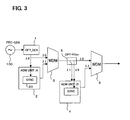
- FIG. 3 shows a conceptual configuration diagram of a transmission system according to the present invention.
- a PRC-level clock being output from a clock source 100 is transmitted from ADM (Add Drop Multiplexing) units 2, 4 in an optical signal form without providing a clock regenerative repeating function, so that the network is operated in synchronization with one reference clock.
- ADM Additional Down Multiplexing
- Clock source (PRC-GEN) 100 of PRC-level accuracy functioning as a network reference clock is constituted by, for example, a cesium atomic oscillator.
- The-reference clock is converted into an optical clock signal by means of an optical clock signal generator (OPT-GEN) 1.
- OPT-GEN optical clock signal generator
- a wavelength converted into an optical clock signal is defined as ⁇ 0.
- ADM unit 2 receives the optical clock signal having wavelength ⁇ 0 to define as a reference clock in the unit. Also, an optical signal including main signal data is transmitted from ADM unit 2 with a wavelength ⁇ 1.
- the output optical signal having wavelength ⁇ 1 is a signal being synchronized into wavelength ⁇ 0 in a synchronization portion 20.
- These two wavelengths ⁇ 0 an ⁇ 1 are optically multiplexed into one optical signal being transmitted through a single optical fiber line in a wavelength multiplexing (WDM) unit 3, to forward to a succeeding node.
- WDM wavelength multiplexing
- the wavelength ⁇ 0 is demultiplexed by an optical filter (OPT-Filter) 5 to feed as a reference clock for use in ADM unit 4.
- OPT-Filter optical filter
- a main signal data having wavelength ⁇ 1 is processed.
- the main signal data having been processed is transmitted from ADM unit 4 to a succeeding node using a wavelength of either ⁇ 1 or ⁇ 2.
- the main signal data having wavelength ⁇ 1 or ⁇ 2 ⁇ 2 is wavelength-multiplexed with the reference clock of wavelength ⁇ 0 in a wavelength multiplexing unit 6.
- a reference clock can be distributed throughout a network without regenerative repeating.
- any ADM units in the nodes can directly face to clock source 100 without intervention of intermediate units. Accordingly, it becomes possible to relay clock signals without being influenced by a network configuration, clock regeneration capability in each unit, etc.
- FIG. 4 shows an embodiment of the present invention, in which an optical signal is wavelength-multiplexed to transmit on an optical fiber line 200.
- 10 Gbps signals for transmission are optically multiplexed into 32 wavelengths.
- only four waves out of 32 waves are illustrated.
- clock source 100 constitutes an optical clock signal generation unit 100-1 together with optical clock signal generator 1.
- An optical clock signal being converted into an optical signal from a reference clock constituted by an electric clock of, for example, 10 MHz generated from clock source 100 constituting optical clock signal generation unit 100-1 is transmitted through an optical clock signal transfer route shown by bold lines.
- the reference clock is converted into a corresponding optical clock signal in optical clock signal generator 1, to branch without modification for distributing to each unit in a similar manner.
- the quality level of the reference clock distributed to the entire units can be maintained equally.
- an optical clock signal having wavelength of ⁇ 0 being output from optical clock signal generator 1 is input to wavelength multiplexing unit 3 on the transmission side.
- transmission terminals (A1 - A4) 10 - 13 data signals of 10 Gbps are respectively converted into optical signals having wavelengths ⁇ 1 - ⁇ 3 referenced by an electric clock signal being output from clock source 100.
- wavelength multiplexing unit 3 on the transmission side transmits through optical fiber cable 200 wavelength-multiplexed signals containing both optical signals having wavelength of ⁇ 1 - ⁇ 3 and the optical clock signal having wavelength of ⁇ 0 generated from optical clock signal generation unit 100-1.
- a wavelength demultiplexing unit 5 on the reception side has an optical filtering function to demultiplex the wavelength-multiplexed optical signal on a per wavelength basis to forward to each corresponding unit. Namely, wavelength demultiplexing unit 5 on the reception side makes the optical clock signal having wavelength ⁇ 0 to branch, and converts the branch signal into an electric signal in optical/electric signal converter 7 to input to ADM units 14, 15.
- the optical signals having wavelength ⁇ 3, ⁇ 4 are made to branch to input to ADM units 14, 15.
- the branching optical signals having wavelengths ⁇ 3, ⁇ 4 are processed being referenced by the optical clock signal having wavelength ⁇ 0.
- the optical clock signal having wavelength ⁇ 0 passes through wavelength demultiplexing unit 5 on the reception side.
- the optical clock signal is wavelength-multiplexed on the transmission side with wavelengths ⁇ 3, ⁇ 4 corresponding to data inserted by ADM units 14, 15 in wavelength multiplexing unit 6, to forward to a succeeding node. Similar process is carried out in the succeeding node.
- the whole network operates in synchronization with the highly accurate optical clock signal, thus enabling to improve clock accuracy of the network as a whole. Therefore, noise accumulation by individual PLL circuits in the ADM units which occurs in the conventional method is not produced.
- dotted lines denote a flow of indication information, which enables to transfer, for example, alarm information which will be described later by inserting additional information into the optical clock signal of wavelength ⁇ 0.
- clock distribution in the network is transmitted through a different optical signal from the main signal to distribute.
- a reference clock being output from a cesium atomic oscillator provided as clock source 100 is converted into an optical clock signal without modification to distribute throughout the network.
- WDM wavelength multiplexing
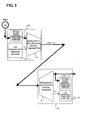
- FIG. 5 is a diagram showing a configuration example of optical clock signal generation unit 100-1 shown in FIG. 4.
- Clock source 100 is an oscillator having accuracy no less than PRC specified by ITU-T, for example cesium atomic oscillator or the like.
- Optical clock signal generator 1 includes an analog-to-digital converter 1-1 and an electric-optical converter 1-2.
- Analog-to-digital converter 1-1 converts an analog clock signal being output from high accuracy clock source 100 such as cesium atomic oscillator to a digital signal to forward to electric-optical converter 1-2.
- Electric-optical converter 1-2 has a function of converting an input digital clock signal to a light having an arbitrary wavelength.
- a digital clock signal is converted into an optical clock signal having a wavelength ⁇ 0.
- a reference clock of an electric signal being output from clock source 100 is directly distributed to terminals 10 - 13 as a clock signal therefor.
- optical clock signal generation unit 100-1 by providing an optical clock signal generation function in optical clock signal generation unit 100-1, it becomes possible to input a clock directly into wavelength multiplexing unit 3, and thus enabling wavelength multiplexing unit 3 to perform clock distribution easily.
- FIG. 6 there is shown a separate configuration of an independent clock source 100 from electric-optical clock signal converter 1.
- An analog clock signal output from a general-purpose reference clock source 100 is received in electric-optical clock signal converter 1.
- analog-to-digital converter 1-1 an analog clock signal from clock source 100 is converted into a corresponding digital signal. Further, an electric-optical modulator 1-2 converts into an optical signal using the digital signal as a modulation signal.
- each terminal 10 - 13 shown in FIG. 4 receives the optical signal as a reference clock.
- an optical-electric (O/E) converter is required in each terminal.
- FIG. 7 is another configuration example of optical clock signal generation unit 100-1.
- a frequency converter 1-3 is provided for receiving an analog clock signal being output from general-purpose reference clock generation unit 100 to convert into a clock frequency for general use in ADM units, etc.
- An electric signal having a frequency being converted by frequency converter 1-3 is converted into an optical clock signal in electric-optical modulator 1-2 to output.
- an analog clock signal generated in a general-purpose clock source 100 is converted into a clock frequency used in ADM units, etc. to forward as an optical clock signal.
- the unit receiving the optical clock signal can use the received clock as a unit clock without conducting frequency conversion. Accordingly, a frequency conversion circuit is not required in such ADM units.
- FIG. 8 shows an embodiment of improvement for discriminating a data signal from a clock signal because the clock signal is wavelength-multiplexed with the data signal according to the present invention.
- a PRC-level reference clock being output from clock source 100 is multicast in an STM frame (125 ⁇ sec)
- a function of inserting an indication information such as a data for wavelength discrimination in an overhead (OHB) part of an STM frame so as to discriminate wavelengths for other data as well as to conduct wavelength management.
- fault information on clock source 100 is inserted into this indication information to distribute.
- the relevant wavelength data is inserted in the SDH/SONET system side.
- the aforementioned indication information denotes SSMB (Synchronous Status Message Byte) information for indicating a synchronous condition, discrimination information denoting a frequency for distributing a clock, fault information, etc.
- SSMB Serial Status Message Byte
- discrimination information denoting a frequency for distributing a clock
- fault information etc.
- optical clock signal generator (SSU/OPT) 1 in FIG. 8 can be realized by a control program the execution of which is controlled by a microcomputer.
- a fault detection function portion 1-10 detects a fault such as halt of the reference clock being input from clock source 100, the detected fault is reported to a non-illustrated microcomputer through a microcomputer interface ( ⁇ -COM INF) 1-17.
- ⁇ -COM INF microcomputer interface
- a clock generation/division portion 1-11 the reference clock input from clock source 100 is converted to generate the clock for STM frame and is divided into predetermined frequencies. Thereafter an STM frame is generated in a frame generation function portion 1-12.
- SSBM information is attached to the generated STM frame overhead by means of microcomputer control through microcomputer interface 1-17. Also, fault information is attached thereto in a fault information attach function portion 1-14. Further, arbitrary information being input from an arbitrary information input portion 1-18 is attached in arbitrary information attach function portion 1-15.
- the STM frame to which the aforementioned information has been attached is converted into an optical clock signal in an electric-optical (E/O) conversion function portion 1-16 to output to wavelength multiplexing (DWDM) unit 3.
- E/O electric-optical
- DWDM wavelength multiplexing
- the reference clock is suspended to output from clock generation/division function portion 1-11 for distributing to each SDH unit 30.
- an optical signal to which indication information (SSMB information) and clock signal discrimination information are applied in optical clock signal generator (SSU/OPT) 1 is transmitted to the neighboring DWDM unit 3.
- DWDM unit 3 On receipt of this optical signal, DWDM unit 3 extracts the indication information from the overhead. It is possible to extract from this optical signal the clock signal discrimination information (identifying the signal concerned is a clock distribution signal) and SSMB information related to the clock signal. Accordingly, it becomes possible to recognize reference clock quality information (PRC) being generated and output from clock source 100. Based on these information sets, each unit performs clock extraction to realize network synchronization.
- the clock signal discrimination information identifying the signal concerned is a clock distribution signal
- SSMB information related to the clock signal Accordingly, it becomes possible to recognize reference clock quality information (PRC) being generated and output from clock source 100. Based on these information sets, each unit performs clock extraction to realize network synchronization.
- PRC reference clock quality information
- FIG. 9 A configuration example of this embodiment is shown in FIG. 9.
- an optical clock conversion function portion 1 is incorporated in an SDH/SONET optical transmission unit 10.
- An optical clock signal is superposed to the optical main signal data being output from SDH transmitting function portion 10-1 by wavelength multiplexing optical transmitter 3.
- wavelength ⁇ 0 of the optical clock signal and wavelength ⁇ 1 of the main signal are demultiplexed in wavelength multiplexing optical receiver 4, to input to an optical clock signal receiving function portion 10-2 and an SDH receiving function portion 10-3, respectively.
- a unit for constituting an optical clock signal distribution system is realized.
- FIG. 10 shows an exemplary system configuration.
- a PRC-level clock signal from clock source 100 is converted into an optical clock signal of wavelength ⁇ 0.
- This optical clock signal is made to branch in an optical coupler 8 and these branch signals are transmitted through different fiber routes, to form a redundant configuration.
- wavelength multiplexing unit 3 includes a work unit 3-1 and a protection unit 3-2.
- a main signal wavelength incoming from an ADM unit and an optical clock signal wavelength are wavelength-multiplexed in a similar manner to that shown in FIG. 3. This may be applied to any other embodiments described later.
- optical filter includes a filter 5-1 for the work side and a filter 5-2 for the protection side.
- ADM unit 4 an optical clock signal on either the work side 5-1 or the protection side 5-2 is selectively received in a clock signal selector 4-1.
- FIG. 11 shows an embodiment for implementing another redundant configuration.
- one side of the optical clock signal of wavelength ⁇ 0 branching in optical coupler 8 is input to a wavelength converter 9.
- the optical clock signal having wavelength ⁇ 0 being input to wavelength converter 9 is converted into a different wavelength ⁇ 2.
- the optical clock signal of wavelength ⁇ 0 having branched in optical coupler 8 and the optical clock signal of wavelength ⁇ 2 having been wavelength-converted in wavelength converter 9 are wavelength-multiplexed in wavelength multiplexing/demultiplexing unit 3 having a non-redundant configuration and is output.
- an optical clock signal of wavelength ⁇ 0 and an optical clock signal of wavelength ⁇ 2 are input separately, and either one of the optical clock signal is selectively received in clock signal selector 4-1.
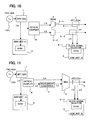
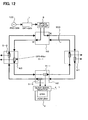
- FIG. 12 shows a redundant configuration in case the present invention is applied to a network of ring configuration.
- each node N0 - N3 is connected in the ring shape by means of a bidirectional optical line 300.
- optical clock signal generator 1 a PRC-level reference clock from clock source 100 is converted into an optical clock signal. Thereafter the optical clock signal is forwarded to both clockwise and counterclockwise direction of bidirectional optical line 300 from optical coupler 8.
- each node N0 - N3 the optical clock signal having wavelength ⁇ 0 is made to branch by optical filters 5-1, 5-2.
- clock selector 4-1 of ADM unit 4 either one of optical clock signal is made to branch.
- network synchronization can be maintained by selecting an optical clock signal being transmitted in the direction opposite to the optical clock signal direction being selected at that time.
- FIG. 13 shows an embodiment of still another redundant configuration.
- two clock sources 100, 100-1 are provided for outputting PRC-level clock signals: primary clock signal and secondary clock signal in place of optical coupler 8.
- optical clock signal generators 1, 1-3 optical clock signals respectively having wavelengths of ⁇ X, ⁇ Y are generated to output.
- optical clock signals having wavelengths ⁇ X, ⁇ Y are independently transmitted through fiber routes 300-1, 300-2, respectively. These optical clock signals are input into clock signal selector 3-1 of ADM unit 3 directly from optical clock signal generators 1, 1-3, or into clock signal selector 4-1 of ADM unit 4 after branching through optical filters 5-1, 5-2, to select either of the optical clock signals to receive.
- clock signal selector 3-1 of ADM unit 3 directly from optical clock signal generators 1, 1-3
- clock signal selector 4-1 of ADM unit 4 after branching through optical filters 5-1, 5-2, to select either of the optical clock signals to receive.
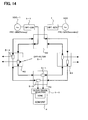
- FIG. 14 shows an example in which the embodiment configuration shown in FIG. 13 is applied to a ring configuration network.
- one optical clock signal from one optical clock signal generator 1 is made to branch in both the clockwise direction and the counterclockwise direction by means of optical coupler 8, to forward to optical fiber transmission lines.
- optical clock signals from independent optical clock signal generators 1, 1-3 are respectively forwarded to either of the two optical fiber transmission lines; one in the clockwise direction and the other in the counterclockwise direction.
- FIG. 15 shows a configuration example in which the configuration shown in FIG. 13 is extended.
- clock sources 100, 100-1 for generating a PRC-level reference clocks for the work side and the protection side, as well as corresponding optical clock signal generators 1, 1-1.
- Clock source 100 and optical clock signal generator 1 as well as clock source 100-1 and optical clock signal generator 1-1 are respectively provided at the both end of the network.
- the optical clock signals are input from both ends of the network to transmit to the opposite ends.
- each ADM unit 4 optical clock signals of the upward direction and the downward direction being separated by optical filters 5, 5-1 are input.
- ADM unit 4 switches to select so as to receive the optical clock signal from the opposite direction in clock selector 4-1.
- the entire transmission units are synchronized simultaneously against the identical optical clock signal, it becomes possible to provide a network in which response capability (shortening of response time) against a network clock is improved.
- the present invention using with wavelength division multiplexing technology, it becomes possible to transmit an optical clock signal through the same optical transmission line as that used for main signal network, and thus the method of the present invention enables to implement without installing another new optical transmission line.
- each unit connected with a network synchronizes in one-to-one correspondence with a PRC-level clock signal, resulting in improved clock accuracy.
- an optical clock signal network as a unit clock source, it becomes possible to omit an inherently unnecessary synchronization circuit of optical signal line (main signal line), in other words to reduce scale of a clock circuit as much as possible.
- network synchronization can be maintained even in case a fault occurs.
Landscapes
- Engineering & Computer Science (AREA)
- Computer Networks & Wireless Communication (AREA)
- Signal Processing (AREA)
- Optical Communication System (AREA)
- Time-Division Multiplex Systems (AREA)
- Synchronisation In Digital Transmission Systems (AREA)
Abstract
Claims (10)
- Réseau WDM comprenant :un générateur d'horloge optique (1) destiné à convertir un signal d'horloge de niveau PRC, Horloge de Référence Primaire, en un signal d'horloge optique ayant une longueur d'onde λ0 ;un multiplexeur en longueur d'onde (3) destiné à multiplexer en longueur d'onde ledit signal d'horloge optique ayant la longueur d'onde λ0 conjointement avec d'autres données de longueur d'onde optiques ; etun démultiplexeur en longueur d'onde (4) prévu dans une unité dudit réseau, destiné à démultiplexer en longueur d'onde ledit signal d'horloge optique ayant la longueur d'onde λ0,dans lequel lesdites autres données de longueur d'onde optiques sont traitées dans ladite unité du réseau en utilisant ledit signal d'horloge optique démultiplexé en longueur d'onde ayant la longueur d'onde λ0 en tant qu'horloge de référence ;
caractérisé en ce que ledit réseau WDM entier est conçu pour fonctionner en synchronisation avec ledit signal d'horloge optique ayant la longueur d'onde λ0. - Réseau WDM selon la revendication 1, comprenant en outre :un convertisseur de longueur d'onde (9) destiné à joindre des informations d'indication audit signal d'horloge, et à effectuer une conversion de longueur d'onde desdites informations d'indication en ledit signal d'horloge optique ayant la longueur d'onde λ0.
- Réseau WDM selon la revendication 2, comprenant en outre :une source d'horloge (100) fournissant ledit signal d'horloge de niveau PRC, Horloge de Référence Primaire, en tant que signal analogique électrique,dans lequel ledit convertisseur de longueur d'onde comprend un convertisseur analogique-numérique destiné à convertir ledit signal analogique électrique provenant de ladite source d'horloge en un signal numérique, de façon à ce qu'un signal d'horloge optique soit configuré en modulant ledit signal optique ayant la longueur d'onde λ0 en utilisant ledit signal numérique obtenu dans ledit convertisseur analogique-numérique en tant que signal de modulation.
- Réseau WDM selon la revendication 3, comprenant en outre :un circuit de conversion de fréquence prévu dans l'étage suivant dudit convertisseur analogique-numérique destiné à convertir une sortie dudit convertisseur analogique-numérique en un signal ayant une fréquence correspondant à une unité de multiplexage à insertion/extraction (ADM) vers laquelle ledit signal d'horloge optique doit être acheminé.
- Réseau WDM selon la revendication 1, comprenant en outre :un coupleur optique (8) faisant bifurquer ledit signal d'horloge optique en deux signaux de bifurcation ;une ligne de transmission optique de travail (300-1) et une ligne de transmission optique de protection (300-2) destinées à transmettre séparément l'un et l'autre desdits signaux d'horloge optiques de bifurcation produits par ledit coupleur optique ; etun sélecteur de signal d'horloge (4-1) prévu dans ladite unité dans le réseau destiné à sélectionner l'un ou l'autre desdits deux signaux d'horloge optiques de bifurcation transmis sur ladite ligne de transmission optique de travail ou ladite ligne de transmission optique de protection.
- Réseau WDM selon la revendication 5, comprenant en outre :un convertisseur de longueur d'onde (9) destiné à convertir en longueur d'onde l'un ou l'autre desdits signaux d'horloge optiques de bifurcation ; etune unité de multiplexage en longueur d'onde (3) destinée à multiplexer en longueur d'onde l'autre desdits deux signaux d'horloge optiques de bifurcation avec ledit signal d'horloge optique converti en longueur d'onde obtenu à partir dudit convertisseur de longueur d'onde,dans lequel des signaux d'horloge optiques pour un côté travail et un côté protection sont transmis sur une ligne de transmission optique commune, de façon à ce qu'une configuration redondante dudit système de distribution d'horloge optique soit réalisée.
- Réseau WDM selon la revendication 5,
dans lequel ledit réseau comprend une ligne de transmission optique bidirectionnelle d'une configuration en anneau, et
dans lequel lesdits deux signaux d'horloge optiques de bifurcation sont transmis mutuellement dans le sens opposé sur ladite ligne de transmission optique bidirectionnelle, de façon à ce qu'une configuration redondante dudit système de distribution d'horloge optique soit réalisée. - Réseau WDM selon la revendication 1, comprenant en outre :une première ligne de transmission optique (300-1) et une deuxième ligne de transmission optique (300-2) ; etun sélecteur de signal d'horloge (4-1) dans ladite unité du réseau,ledit générateur d'horloge optique destiné à convertir des premier et deuxième signaux d'horloge de niveau PRC, Horloge de Référence Primaire, en premier et deuxième signaux d'horloge optiques ayant des première et deuxième longueurs d'onde respectivement ;lesdites première et deuxième lignes de transmission optique destinées à transmettre lesdits premier et deuxième signaux d'horloge optiques ayant lesdites première et deuxième longueurs d'onde respectivement ;ledit multiplexeur en longueur d'onde destiné à multiplexer en longueur d'onde lesdits premier et deuxième signaux d'horloge optiques conjointement avec d'autres données de longueur d'onde optiques ;ledit démultiplexeur en longueur d'onde destiné à démultiplexer en longueur d'onde lesdits premier et deuxième signaux d'horloge optiques ; etledit sélecteur de signal d'horloge destiné à sélectionner un signal d'horloge optique démultiplexé en longueur d'onde ayant soit ladite première longueur d'onde, soit ladite deuxième longueur d'onde.
- Réseau WDM selon la revendication 8,
dans lequel ledit réseau comprend une ligne de transmission optique bidirectionnelle d'une configuration en anneau, et lesdits signaux d'horloge optiques ayant ladite première longueur d'onde et ladite deuxième longueur d'onde générés à partir dudit premier générateur d'horloge optique et dudit deuxième générateur d'horloge optique sont transmis mutuellement dans le sens opposé, de façon à ce qu'une configuration redondante dudit système de distribution d'horloge optique soit réalisée. - Réseau WDM selon la revendication 8,
dans lequel ladite première source d'horloge et ladite deuxième source d'horloge ainsi que ledit premier générateur d'horloge optique et ledit deuxième générateur d'horloge optique correspondant respectivement auxdites première et deuxième sources d'horloge sont disposés aux deux extrémités desdites lignes de transmission optique.
Applications Claiming Priority (1)
| Application Number | Priority Date | Filing Date | Title |
|---|---|---|---|
| PCT/JP2000/002578 WO2001080478A1 (fr) | 2000-04-19 | 2000-04-19 | Systeme de distribution de signal d'horloge optique dans un reseau mrl |
Publications (3)
| Publication Number | Publication Date |
|---|---|
| EP1280294A1 EP1280294A1 (fr) | 2003-01-29 |
| EP1280294A4 EP1280294A4 (fr) | 2005-06-15 |
| EP1280294B1 true EP1280294B1 (fr) | 2007-02-14 |
Family
ID=11735941
Family Applications (1)
| Application Number | Title | Priority Date | Filing Date |
|---|---|---|---|
| EP00917377A Expired - Lifetime EP1280294B1 (fr) | 2000-04-19 | 2000-04-19 | Systeme de distribution de signal d'horloge optique dans un reseau a multiplexage par repartition en longueur d'onde |
Country Status (6)
| Country | Link |
|---|---|
| US (1) | US7024121B2 (fr) |
| EP (1) | EP1280294B1 (fr) |
| JP (1) | JP3824539B2 (fr) |
| CN (1) | CN100361434C (fr) |
| DE (1) | DE60033442D1 (fr) |
| WO (1) | WO2001080478A1 (fr) |
Families Citing this family (26)
| Publication number | Priority date | Publication date | Assignee | Title |
|---|---|---|---|---|
| US20030133651A1 (en) * | 2002-01-16 | 2003-07-17 | Teraphase Technologies, Inc. | Filtering noise in optical signal transmission |
| US7248802B2 (en) * | 2002-11-27 | 2007-07-24 | Nokia Corporation | Distribution of a synchronization signal in an optical communication system |
| CN1784843A (zh) * | 2003-05-07 | 2006-06-07 | 皇家飞利浦电子股份有限公司 | 通信系统 |
| DE10360017A1 (de) * | 2003-12-19 | 2005-07-21 | Siemens Ag | Audio- und/oder Videosystem für ein Kraftfahrzeug |
| DE102004004843B4 (de) * | 2004-01-30 | 2010-07-22 | Siemens Ag | Bussystem zur Steuerung einer Komponente einer Druckmaschine und entsprechendes Verfahren |
| EP1583266A3 (fr) * | 2004-03-31 | 2007-07-11 | Tellabs Denmark A/S | Synchronisation de services MRT sur réseaux de paquets |
| US20060039347A1 (en) * | 2004-08-18 | 2006-02-23 | Fujitsu Limited | Synchronous transmission network system |
| JP2006279355A (ja) * | 2005-03-28 | 2006-10-12 | Nec Corp | 波長分割多重伝送システム、波長分割多重伝送装置及び波長分割多重伝送装置の制御方法 |
| US8588613B1 (en) * | 2007-12-27 | 2013-11-19 | At&T Intellectual Property I, L.P. | Sync distribution over a non-traffic bearing channel |
| TWI378661B (en) * | 2008-01-04 | 2012-12-01 | Amtran Technology Co Ltd | Data transmission system using optical fiber and home entertainment system using hdcp |
| WO2009134223A1 (fr) * | 2008-04-30 | 2009-11-05 | Hewlett-Packard Development Company, L.P. | Distribution d’un signal d’horloge optique intentionnellement asymétrique |
| FI121771B (fi) | 2009-01-16 | 2011-03-31 | Tellabs Oy | Menetelmä ja järjestely kellosignaalin säätämiseksi |
| JP4725651B2 (ja) * | 2009-01-22 | 2011-07-13 | 沖電気工業株式会社 | 受動光ネットワーク通信システム |
| CN102457372B (zh) * | 2010-11-02 | 2014-10-29 | 上海中兴软件有限责任公司 | 一种通信系统以及利用光纤传输时钟信号的方法 |
| US8493123B2 (en) * | 2010-12-15 | 2013-07-23 | Raytheon Company | Synchronization of remote clocks |
| US8565609B2 (en) * | 2010-12-15 | 2013-10-22 | Raytheon Company | Distribution system for optical reference |
| US9252904B2 (en) * | 2011-06-01 | 2016-02-02 | Coriant Operations, Inc. | Method and apparatus for distributing network timing in a mesh optical network |
| JP5998819B2 (ja) * | 2012-10-09 | 2016-09-28 | 富士通株式会社 | 光信号送信装置、光周波数分割多重伝送システムおよび光信号通信方法 |
| US9191112B2 (en) | 2013-08-07 | 2015-11-17 | Raytheon Company | Analog optical fiber-based signal distribution system and method |
| JP6053232B2 (ja) * | 2013-10-25 | 2016-12-27 | 日本電信電話株式会社 | 光通信システム及び光通信異常復帰方法 |
| CN105591697B (zh) * | 2016-01-20 | 2018-04-17 | 中国科学院上海光学精密机械研究所 | 高精度光纤时频环形组网系统和组网方法 |
| US10211971B2 (en) * | 2016-08-30 | 2019-02-19 | Finisar Corporation | Bi-directional transceiver with time synchronization |
| JP7007668B2 (ja) * | 2018-05-30 | 2022-01-24 | 日本電信電話株式会社 | 光ファイバリンクおよび中継ノード |
| US12034481B2 (en) * | 2020-09-15 | 2024-07-09 | California Institute Of Technology | Optically enabled RF phased-arrays for data transmission |
| WO2022081614A1 (fr) | 2020-10-12 | 2022-04-21 | California Institute Of Technology | Réseaux à commande de phase rf activés par voie optique pour la réception de données |
| GB2633816A (en) * | 2023-09-22 | 2025-03-26 | Bae Systems Plc | LDEW optical data link |
Family Cites Families (22)
| Publication number | Priority date | Publication date | Assignee | Title |
|---|---|---|---|---|
| JPS5866442A (ja) | 1981-10-16 | 1983-04-20 | Fujitsu Ltd | 光ハイウエイフレ−ム同期回路 |
| JPS59172844A (ja) * | 1983-03-22 | 1984-09-29 | Fujitsu Ltd | クロツク供給方式 |
| JPS6451736A (en) * | 1987-08-21 | 1989-02-28 | Fujitsu Ltd | Coherent light communication system |
| JPH01144832A (ja) * | 1987-12-01 | 1989-06-07 | Nec Corp | タイミング情報光並送方式 |
| JPH01233936A (ja) * | 1988-03-15 | 1989-09-19 | Nec Corp | クロック信号伝送回路 |
| JPH04152725A (ja) * | 1990-10-17 | 1992-05-26 | Hitachi Ltd | マスタークロック分配方法およびそれを用いた装置 |
| JP3083118B2 (ja) * | 1992-02-08 | 2000-09-04 | キヤノン株式会社 | 光通信障害検出方法及びその方法を用いた光通信システム |
| JPH05252180A (ja) * | 1992-03-05 | 1993-09-28 | Nec Corp | クロック切替方式 |
| JPH05335904A (ja) * | 1992-06-02 | 1993-12-17 | Yokogawa Electric Corp | クロック信号発生回路 |
| JPH0779216A (ja) | 1993-09-08 | 1995-03-20 | Nec Corp | 情報送受信装置 |
| US5615035A (en) * | 1993-09-24 | 1997-03-25 | Gte Laboratories Incorporated | Photonic dual bus for wide-area CATV broadcast and data transport |
| JP2600595B2 (ja) * | 1993-12-06 | 1997-04-16 | 日本電気株式会社 | クロック分配方式 |
| ATE180937T1 (de) * | 1994-03-15 | 1999-06-15 | Siemens Ag | Verfahren zur empfangsseitigen taktversorgung für digital mittels atm übertragene videosignale in faser-/koaxial-teilnehmeranschlussnetzen |
| JP2626580B2 (ja) | 1994-10-20 | 1997-07-02 | 日本電気株式会社 | 多重化光中継装置 |
| JP3019756B2 (ja) * | 1995-10-05 | 2000-03-13 | 日本電気株式会社 | Add/drop方法と同期方法 |
| JPH10322379A (ja) * | 1997-05-21 | 1998-12-04 | Nec Miyagi Ltd | クロックパス切替方法 |
| JPH1112278A (ja) * | 1997-06-18 | 1999-01-19 | Dainippon Pharmaceut Co Ltd | ピリドンカルボン酸誘導体、そのエステルまたはこれらの塩 |
| JPH11122207A (ja) * | 1997-10-14 | 1999-04-30 | Fujitsu Ltd | 伝送装置および同期ネットワークにおける信号伝送方法 |
| JPH11122278A (ja) * | 1997-10-15 | 1999-04-30 | Nec Corp | 網同期ネットワークシステム及びこれに用いる送受信装置 |
| US20020075536A1 (en) * | 1998-06-30 | 2002-06-20 | Xiang-Dong Cao | Multi-wavelength all-optical regenerators ( mars) |
| JP2000029561A (ja) * | 1998-07-08 | 2000-01-28 | Nec Kofu Ltd | クロック供給回路 |
| DE19959815A1 (de) * | 1999-12-11 | 2001-06-21 | Alcatel Sa | Synchrones digitales Nachrichtenübertragungssystem |
-
2000
- 2000-04-19 JP JP2001576607A patent/JP3824539B2/ja not_active Expired - Fee Related
- 2000-04-19 EP EP00917377A patent/EP1280294B1/fr not_active Expired - Lifetime
- 2000-04-19 DE DE60033442T patent/DE60033442D1/de not_active Expired - Lifetime
- 2000-04-19 CN CNB008196591A patent/CN100361434C/zh not_active Expired - Fee Related
- 2000-04-19 WO PCT/JP2000/002578 patent/WO2001080478A1/fr not_active Ceased
-
2002
- 2002-10-17 US US10/274,537 patent/US7024121B2/en not_active Expired - Fee Related
Also Published As
| Publication number | Publication date |
|---|---|
| WO2001080478A1 (fr) | 2001-10-25 |
| EP1280294A4 (fr) | 2005-06-15 |
| US20030059160A1 (en) | 2003-03-27 |
| DE60033442D1 (de) | 2007-03-29 |
| US7024121B2 (en) | 2006-04-04 |
| CN100361434C (zh) | 2008-01-09 |
| EP1280294A1 (fr) | 2003-01-29 |
| JP3824539B2 (ja) | 2006-09-20 |
| CN1454418A (zh) | 2003-11-05 |
Similar Documents
| Publication | Publication Date | Title |
|---|---|---|
| EP1280294B1 (fr) | Systeme de distribution de signal d'horloge optique dans un reseau a multiplexage par repartition en longueur d'onde | |
| EP0721275B1 (fr) | Système de commande de fonctionnement et de maintenance dans un réseau optique | |
| JPWO2001080478A1 (ja) | Wdmネットワークの光クロック信号分配システム | |
| Manchester et al. | The evolution of transport network survivability | |
| RU2331157C2 (ru) | Способ, устройство и система для оптической связи | |
| US6198721B1 (en) | Method and system for data transmission in a ring network | |
| US20040042796A1 (en) | Photonic communication system with "sub-line rate" bandwidth granularity, protocol transparency and deterministic mesh connectivity | |
| JP5132778B2 (ja) | 光ネットワークシステム、光冗長切替え装置およびwdm装置 | |
| JP2001230759A (ja) | 波長多重伝送システム、それに用いる装置 | |
| JP2002223197A (ja) | 品質管理機能を有する光ネットワークシステム | |
| JP2001069087A (ja) | 追加/削除配置、追加/削除方法、及び通信システム | |
| US6594047B1 (en) | Apparatus and method for providing optical channel overhead in optical transport networks | |
| EP1056235A2 (fr) | Système d'anneau optique | |
| JP5681394B2 (ja) | 光電気ハイブリッドノード | |
| US6738579B2 (en) | Synchronous digital communications system | |
| US20010038475A1 (en) | Synchronous digital communications system | |
| EP1511331B1 (fr) | Controleur permettant de commuter un signal optique multiplexe en longueur d'onde | |
| KR100256689B1 (ko) | 분기 결합용 광전송 장치 | |
| JP3788263B2 (ja) | 通信ネットワーク、通信ネットワーク・ノード装置、及び、障害回復方式 | |
| JP3369965B2 (ja) | 光波長多重化伝送システムにおける監視制御装置 | |
| JP3351365B2 (ja) | 通信ネットワーク、通信ノード、及び、障害回復方法 | |
| US20150171990A1 (en) | Transmission device, transmission system, and transmission method | |
| JP3324988B2 (ja) | 光パス信号終端装置および光パス信号装置 | |
| JP4432618B2 (ja) | 光通信装置 | |
| JPH11112422A (ja) | 波長多重網切替え装置及び波長多重リング光ネットワーク・システム |
Legal Events
| Date | Code | Title | Description |
|---|---|---|---|
| PUAI | Public reference made under article 153(3) epc to a published international application that has entered the european phase |
Free format text: ORIGINAL CODE: 0009012 |
|
| 17P | Request for examination filed |
Effective date: 20021018 |
|
| AK | Designated contracting states |
Designated state(s): AT BE CH CY DE DK ES FI FR GB GR IE IT LI LU MC NL PT SE |
|
| RBV | Designated contracting states (corrected) |
Designated state(s): AT BE CH DE FR GB LI |
|
| A4 | Supplementary search report drawn up and despatched |
Effective date: 20050503 |
|
| GRAP | Despatch of communication of intention to grant a patent |
Free format text: ORIGINAL CODE: EPIDOSNIGR1 |
|
| RBV | Designated contracting states (corrected) |
Designated state(s): DE FR GB |
|
| GRAS | Grant fee paid |
Free format text: ORIGINAL CODE: EPIDOSNIGR3 |
|
| GRAA | (expected) grant |
Free format text: ORIGINAL CODE: 0009210 |
|
| AK | Designated contracting states |
Kind code of ref document: B1 Designated state(s): DE FR GB |
|
| REG | Reference to a national code |
Ref country code: GB Ref legal event code: FG4D |
|
| REF | Corresponds to: |
Ref document number: 60033442 Country of ref document: DE Date of ref document: 20070329 Kind code of ref document: P |
|
| ET | Fr: translation filed | ||
| PLBE | No opposition filed within time limit |
Free format text: ORIGINAL CODE: 0009261 |
|
| STAA | Information on the status of an ep patent application or granted ep patent |
Free format text: STATUS: NO OPPOSITION FILED WITHIN TIME LIMIT |
|
| 26N | No opposition filed |
Effective date: 20071115 |
|
| PG25 | Lapsed in a contracting state [announced via postgrant information from national office to epo] |
Ref country code: DE Free format text: LAPSE BECAUSE OF FAILURE TO SUBMIT A TRANSLATION OF THE DESCRIPTION OR TO PAY THE FEE WITHIN THE PRESCRIBED TIME-LIMIT Effective date: 20070515 |
|
| REG | Reference to a national code |
Ref country code: FR Ref legal event code: PLFP Year of fee payment: 17 |
|
| PGFP | Annual fee paid to national office [announced via postgrant information from national office to epo] |
Ref country code: FR Payment date: 20160309 Year of fee payment: 17 |
|
| PGFP | Annual fee paid to national office [announced via postgrant information from national office to epo] |
Ref country code: GB Payment date: 20160413 Year of fee payment: 17 |
|
| GBPC | Gb: european patent ceased through non-payment of renewal fee |
Effective date: 20170419 |
|
| REG | Reference to a national code |
Ref country code: FR Ref legal event code: ST Effective date: 20171229 |
|
| PG25 | Lapsed in a contracting state [announced via postgrant information from national office to epo] |
Ref country code: FR Free format text: LAPSE BECAUSE OF NON-PAYMENT OF DUE FEES Effective date: 20170502 |
|
| PG25 | Lapsed in a contracting state [announced via postgrant information from national office to epo] |
Ref country code: GB Free format text: LAPSE BECAUSE OF NON-PAYMENT OF DUE FEES Effective date: 20170419 |