EP1320286A2 - Elektronischer Modul mit bei niedriger Temperatur gleichzeitig gebranntem keramischem (LTCC) Substrat mit darin eingebetteter kapazitiever Struktur und zugehörige Verfahren - Google Patents
Elektronischer Modul mit bei niedriger Temperatur gleichzeitig gebranntem keramischem (LTCC) Substrat mit darin eingebetteter kapazitiever Struktur und zugehörige Verfahren Download PDFInfo
- Publication number
- EP1320286A2 EP1320286A2 EP02027617A EP02027617A EP1320286A2 EP 1320286 A2 EP1320286 A2 EP 1320286A2 EP 02027617 A EP02027617 A EP 02027617A EP 02027617 A EP02027617 A EP 02027617A EP 1320286 A2 EP1320286 A2 EP 1320286A2
- Authority
- EP
- European Patent Office
- Prior art keywords
- dielectric layer
- capacitive structure
- electronic module
- outer dielectric
- layers
- Prior art date
- Legal status (The legal status is an assumption and is not a legal conclusion. Google has not performed a legal analysis and makes no representation as to the accuracy of the status listed.)
- Granted
Links
Images


Classifications
-
- H—ELECTRICITY
- H10—SEMICONDUCTOR DEVICES; ELECTRIC SOLID-STATE DEVICES NOT OTHERWISE PROVIDED FOR
- H10W—GENERIC PACKAGES, INTERCONNECTIONS, CONNECTORS OR OTHER CONSTRUCTIONAL DETAILS OF DEVICES COVERED BY CLASS H10
- H10W70/00—Package substrates; Interposers; Redistribution layers [RDL]
- H10W70/60—Insulating or insulated package substrates; Interposers; Redistribution layers
- H10W70/67—Insulating or insulated package substrates; Interposers; Redistribution layers characterised by their insulating layers or insulating parts
- H10W70/68—Shapes or dispositions thereof
- H10W70/685—Shapes or dispositions thereof comprising multiple insulating layers
-
- H—ELECTRICITY
- H05—ELECTRIC TECHNIQUES NOT OTHERWISE PROVIDED FOR
- H05K—PRINTED CIRCUITS; CASINGS OR CONSTRUCTIONAL DETAILS OF ELECTRIC APPARATUS; MANUFACTURE OF ASSEMBLAGES OF ELECTRICAL COMPONENTS
- H05K1/00—Printed circuits
- H05K1/16—Printed circuits incorporating printed electric components, e.g. printed resistors, capacitors or inductors
- H05K1/162—Printed circuits incorporating printed electric components, e.g. printed resistors, capacitors or inductors incorporating printed capacitors
-
- H—ELECTRICITY
- H10—SEMICONDUCTOR DEVICES; ELECTRIC SOLID-STATE DEVICES NOT OTHERWISE PROVIDED FOR
- H10W—GENERIC PACKAGES, INTERCONNECTIONS, CONNECTORS OR OTHER CONSTRUCTIONAL DETAILS OF DEVICES COVERED BY CLASS H10
- H10W44/00—Electrical arrangements for controlling or matching impedance
- H10W44/601—Capacitive arrangements
-
- H—ELECTRICITY
- H05—ELECTRIC TECHNIQUES NOT OTHERWISE PROVIDED FOR
- H05K—PRINTED CIRCUITS; CASINGS OR CONSTRUCTIONAL DETAILS OF ELECTRIC APPARATUS; MANUFACTURE OF ASSEMBLAGES OF ELECTRICAL COMPONENTS
- H05K1/00—Printed circuits
- H05K1/02—Details
- H05K1/03—Use of materials for the substrate
- H05K1/0306—Inorganic insulating substrates, e.g. ceramic, glass
-
- H—ELECTRICITY
- H05—ELECTRIC TECHNIQUES NOT OTHERWISE PROVIDED FOR
- H05K—PRINTED CIRCUITS; CASINGS OR CONSTRUCTIONAL DETAILS OF ELECTRIC APPARATUS; MANUFACTURE OF ASSEMBLAGES OF ELECTRICAL COMPONENTS
- H05K2201/00—Indexing scheme relating to printed circuits covered by H05K1/00
- H05K2201/01—Dielectrics
- H05K2201/0183—Dielectric layers
- H05K2201/0195—Dielectric or adhesive layers comprising a plurality of layers, e.g. in a multilayer structure
-
- H—ELECTRICITY
- H05—ELECTRIC TECHNIQUES NOT OTHERWISE PROVIDED FOR
- H05K—PRINTED CIRCUITS; CASINGS OR CONSTRUCTIONAL DETAILS OF ELECTRIC APPARATUS; MANUFACTURE OF ASSEMBLAGES OF ELECTRICAL COMPONENTS
- H05K2201/00—Indexing scheme relating to printed circuits covered by H05K1/00
- H05K2201/09—Shape and layout
- H05K2201/09209—Shape and layout details of conductors
- H05K2201/09654—Shape and layout details of conductors covering at least two types of conductors provided for in H05K2201/09218 - H05K2201/095
- H05K2201/09672—Superposed layout, i.e. in different planes
-
- H—ELECTRICITY
- H05—ELECTRIC TECHNIQUES NOT OTHERWISE PROVIDED FOR
- H05K—PRINTED CIRCUITS; CASINGS OR CONSTRUCTIONAL DETAILS OF ELECTRIC APPARATUS; MANUFACTURE OF ASSEMBLAGES OF ELECTRICAL COMPONENTS
- H05K3/00—Apparatus or processes for manufacturing printed circuits
- H05K3/46—Manufacturing multilayer circuits
- H05K3/4611—Manufacturing multilayer circuits by laminating two or more circuit boards
- H05K3/4626—Manufacturing multilayer circuits by laminating two or more circuit boards characterised by the insulating layers or materials
- H05K3/4629—Manufacturing multilayer circuits by laminating two or more circuit boards characterised by the insulating layers or materials laminating inorganic sheets comprising printed circuits, e.g. green ceramic sheets
-
- H—ELECTRICITY
- H05—ELECTRIC TECHNIQUES NOT OTHERWISE PROVIDED FOR
- H05K—PRINTED CIRCUITS; CASINGS OR CONSTRUCTIONAL DETAILS OF ELECTRIC APPARATUS; MANUFACTURE OF ASSEMBLAGES OF ELECTRICAL COMPONENTS
- H05K3/00—Apparatus or processes for manufacturing printed circuits
- H05K3/46—Manufacturing multilayer circuits
- H05K3/4688—Composite multilayer circuits, i.e. comprising insulating layers having different properties
-
- H—ELECTRICITY
- H10—SEMICONDUCTOR DEVICES; ELECTRIC SOLID-STATE DEVICES NOT OTHERWISE PROVIDED FOR
- H10W—GENERIC PACKAGES, INTERCONNECTIONS, CONNECTORS OR OTHER CONSTRUCTIONAL DETAILS OF DEVICES COVERED BY CLASS H10
- H10W90/00—Package configurations
- H10W90/701—Package configurations characterised by the relative positions of pads or connectors relative to package parts
- H10W90/731—Package configurations characterised by the relative positions of pads or connectors relative to package parts of die-attach connectors
- H10W90/734—Package configurations characterised by the relative positions of pads or connectors relative to package parts of die-attach connectors between a chip and a stacked insulating package substrate, interposer or RDL
-
- Y—GENERAL TAGGING OF NEW TECHNOLOGICAL DEVELOPMENTS; GENERAL TAGGING OF CROSS-SECTIONAL TECHNOLOGIES SPANNING OVER SEVERAL SECTIONS OF THE IPC; TECHNICAL SUBJECTS COVERED BY FORMER USPC CROSS-REFERENCE ART COLLECTIONS [XRACs] AND DIGESTS
- Y10—TECHNICAL SUBJECTS COVERED BY FORMER USPC
- Y10T—TECHNICAL SUBJECTS COVERED BY FORMER US CLASSIFICATION
- Y10T29/00—Metal working
- Y10T29/49—Method of mechanical manufacture
- Y10T29/49002—Electrical device making
- Y10T29/49117—Conductor or circuit manufacturing
- Y10T29/49124—On flat or curved insulated base, e.g., printed circuit, etc.
- Y10T29/4913—Assembling to base an electrical component, e.g., capacitor, etc.
Definitions
- a typical electronic module may include one or more integrated circuits (ICs), such as microprocessors, etc., as well as other discreet components (e.g., resistors, capacitors, etc.) mounted on a substrate, for example.
- ICs integrated circuits
- LTCC low temperature co-fired ceramics
- FIG. 7 is a bar graph of measured capacitance values for twelve different embedded capacitive structures made according to the invention.
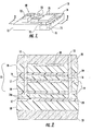
- one or more electronic devices 13 may be mounted on a surface 20 of the LTCC substrate 12, for example, as will be appreciated by those skilled in the art.
- the electronic devices 13 may include semiconductor devices, integrated circuits, heat coils, resistors, etc., for example. Of course, other electronic devices may also be mounted on the electronic module 10.
- the substrate 12, as best seen in FIG. 1, may carry electrical connectors 14 on at least one of its surfaces.
- the electrical connectors 14 may be edge connectors for connection to a ribbon type cable, as shown in FIG. 1, for example.
- other connectors may also be used, such as pins in a pin grid array, as will be appreciated by those skilled in the art.
- the data in Table 2 was generated at 1 MHz using a HP 4278A capacitance meter and a HP 16034E test fixture.
- the temperature coefficient measurements were performed using an Ingalls Engineering model IE-TCM-80 temperature chamber and capacitance test system using a 1KHz test frequency.
- High frequency test results for the low-K materials are shown in Table 3.
- the K10 and K2400 dielectrics provide acceptable COG and X7R performance, respectively, while the K10 data illustrates this material's suitability as a low-K, low-loss substrate dielectric.
- Embedded capacitive structures 11 with capacitances of 0.01, 0.015, 0.02 , 0.1, 0.15, and 0.2 ⁇ F were designed and produced.
- a modified tape transfer manufacturing process was used to fabricate the test structures.
- Dielectric tape was cast on a Mylar carrier film using a floating doctor blade, and the tape thickness used was 25 ⁇ m for the K10 & K14 materials and 14 ⁇ m for the K2400 material.
- Internal conductors were deposited using a vision aligned screen printer.
- a PVB binder system, Ferro B74001, along with Ferro modifiers M1125 and M1135 were used with binder solids loading adjusted for each dielectric composition to help match green and fired shrinkage characteristics.
Landscapes
- Engineering & Computer Science (AREA)
- Microelectronics & Electronic Packaging (AREA)
- Production Of Multi-Layered Print Wiring Board (AREA)
- Fixed Capacitors And Capacitor Manufacturing Machines (AREA)
- Non-Metallic Protective Coatings For Printed Circuits (AREA)
- Parts Printed On Printed Circuit Boards (AREA)
Applications Claiming Priority (2)
| Application Number | Priority Date | Filing Date | Title |
|---|---|---|---|
| US10/022,595 US6985349B2 (en) | 2001-12-13 | 2001-12-13 | Electronic module including a low temperature co-fired ceramic (LTCC) substrate with a capacitive structure embedded therein and related methods |
| US22595 | 2001-12-13 |
Publications (3)
| Publication Number | Publication Date |
|---|---|
| EP1320286A2 true EP1320286A2 (de) | 2003-06-18 |
| EP1320286A3 EP1320286A3 (de) | 2005-01-05 |
| EP1320286B1 EP1320286B1 (de) | 2011-08-17 |
Family
ID=21810412
Family Applications (1)
| Application Number | Title | Priority Date | Filing Date |
|---|---|---|---|
| EP02027617A Expired - Lifetime EP1320286B1 (de) | 2001-12-13 | 2002-12-11 | Elektronischer Modul mit bei niedriger Temperatur gleichzeitig gebranntem keramischem (LTCC) Substrat mit darin eingebetteter kapazitiever Struktur und zugehörige Verfahren |
Country Status (4)
| Country | Link |
|---|---|
| US (2) | US6985349B2 (de) |
| EP (1) | EP1320286B1 (de) |
| JP (1) | JP2003203825A (de) |
| CA (1) | CA2413369A1 (de) |
Cited By (3)
| Publication number | Priority date | Publication date | Assignee | Title |
|---|---|---|---|---|
| DE102007032277A1 (de) * | 2007-07-11 | 2009-01-15 | Epcos Ag | Panel für Modulsubstrate und Verfahren zum elektrischen Testen unbestückter Modulsubstrate |
| WO2016038094A1 (de) * | 2014-09-09 | 2016-03-17 | Ceramtec Gmbh | Mehrlagenkühler |
| CN110312366A (zh) * | 2019-07-03 | 2019-10-08 | 安捷利电子科技(苏州)有限公司 | 埋容材料及其制备工艺、埋容电路板及其制作工艺 |
Families Citing this family (20)
| Publication number | Priority date | Publication date | Assignee | Title |
|---|---|---|---|---|
| US6470545B1 (en) * | 1999-09-15 | 2002-10-29 | National Semiconductor Corporation | Method of making an embedded green multi-layer ceramic chip capacitor in a low-temperature co-fired ceramic (LTCC) substrate |
| KR101047713B1 (ko) | 2003-12-29 | 2011-07-08 | 엘지이노텍 주식회사 | Ltcc 커패시터 |
| US20060163768A1 (en) * | 2005-01-26 | 2006-07-27 | Needes Christopher R | Multi-component LTCC substrate with a core of high dielectric constant ceramic material and processes for the development thereof |
| US20060162844A1 (en) * | 2005-01-26 | 2006-07-27 | Needes Christopher R | Multi-component LTCC substrate with a core of high dielectric constant ceramic material and processes for the development thereof |
| US7548432B2 (en) * | 2005-03-24 | 2009-06-16 | Agency For Science, Technology And Research | Embedded capacitor structure |
| KR100878411B1 (ko) | 2007-01-25 | 2009-01-13 | 삼성전기주식회사 | 캐패시터 내장 세라믹 기판 제조 방법 |
| US7745281B2 (en) * | 2007-03-07 | 2010-06-29 | Kemet Electronics Corporation | Thin solid electrolytic capacitor embeddable in a substrate |
| US7917218B2 (en) | 2007-03-21 | 2011-03-29 | Medtronic, Inc. | Filtering capacitor feedthrough assembly |
| US8195118B2 (en) | 2008-07-15 | 2012-06-05 | Linear Signal, Inc. | Apparatus, system, and method for integrated phase shifting and amplitude control of phased array signals |
| KR100994172B1 (ko) * | 2008-07-23 | 2010-11-15 | 삼화콘덴서공업주식회사 | 커패시터 모듈 |
| DE102008046336A1 (de) * | 2008-09-09 | 2010-03-11 | Osram Gesellschaft mit beschränkter Haftung | LTCC-Schichtstapel |
| US8872719B2 (en) | 2009-11-09 | 2014-10-28 | Linear Signal, Inc. | Apparatus, system, and method for integrated modular phased array tile configuration |
| US8593816B2 (en) | 2011-09-21 | 2013-11-26 | Medtronic, Inc. | Compact connector assembly for implantable medical device |
| KR101514562B1 (ko) * | 2013-11-06 | 2015-04-22 | 삼성전기주식회사 | 적층 세라믹 전자 부품 및 그 실장 기판 |
| US20150264813A1 (en) * | 2014-03-11 | 2015-09-17 | United Microelectronics Corp. | Chip-stack interposer structure including passive device and method for fabricating the same |
| US10610982B2 (en) * | 2015-11-12 | 2020-04-07 | General Electric Company | Weld filler metal for superalloys and methods of making |
| TWI551442B (zh) * | 2015-11-25 | 2016-10-01 | Layered ceramic electronic components and pressureless sintering method co | |
| CN106915958B (zh) * | 2015-12-24 | 2020-10-09 | 华新科技股份有限公司 | 积层电子陶瓷元件及其无压共烧结制法 |
| CN108461483B (zh) * | 2018-04-02 | 2020-03-17 | 华进半导体封装先导技术研发中心有限公司 | 一种嵌入式电容转接板封装结构及制造方法 |
| CN114641840B (zh) | 2019-06-27 | 2025-01-21 | 埃雷克斯组件股份有限公司 | 陶瓷微电子装置及其制造方法 |
Citations (1)
| Publication number | Priority date | Publication date | Assignee | Title |
|---|---|---|---|---|
| US5757611A (en) | 1996-04-12 | 1998-05-26 | Norhtrop Grumman Corporation | Electronic package having buried passive components |
Family Cites Families (28)
| Publication number | Priority date | Publication date | Assignee | Title |
|---|---|---|---|---|
| GB2197540B (en) * | 1986-11-12 | 1991-04-17 | Murata Manufacturing Co | A circuit structure. |
| US4729058A (en) * | 1986-12-11 | 1988-03-01 | Aluminum Company Of America | Self-limiting capacitor formed using a plurality of thin film semiconductor ceramic layers |
| JPH0632384B2 (ja) * | 1987-12-22 | 1994-04-27 | 株式会社住友金属セラミックス | 積層セラミック基板の製造方法 |
| JPH01241810A (ja) * | 1988-03-23 | 1989-09-26 | Nec Corp | 複合積層セラミック構造体 |
| JPH01262695A (ja) * | 1988-04-13 | 1989-10-19 | Nec Corp | コンデンサ素子内蔵セラミック多層基板 |
| JPH0529771A (ja) * | 1991-07-23 | 1993-02-05 | Fujitsu Ltd | セラミツク回路基板およびその製造方法 |
| US5144526A (en) * | 1991-08-05 | 1992-09-01 | Hughes Aircraft Company | Low temperature co-fired ceramic structure containing buried capacitors |
| US5800575A (en) * | 1992-04-06 | 1998-09-01 | Zycon Corporation | In situ method of forming a bypass capacitor element internally within a capacitive PCB |
| JPH05335183A (ja) * | 1992-05-28 | 1993-12-17 | Murata Mfg Co Ltd | 多層基板を備えた電子部品及びその製造方法 |
| JPH06164150A (ja) * | 1992-11-18 | 1994-06-10 | Murata Mfg Co Ltd | セラミック多層基板 |
| US5371403A (en) * | 1993-09-24 | 1994-12-06 | Vlsi Technology, Inc. | High performance package using high dielectric constant materials for power/ground and low dielectric constant materials for signal lines |
| JPH0832242A (ja) * | 1994-07-15 | 1996-02-02 | Tdk Corp | コンデンサ内蔵多層配線基板 |
| JPH08213755A (ja) * | 1995-01-31 | 1996-08-20 | Kyocera Corp | コンデンサ内蔵型積層セラミック回路基板及びその製造方法 |
| US5661882A (en) * | 1995-06-30 | 1997-09-02 | Ferro Corporation | Method of integrating electronic components into electronic circuit structures made using LTCC tape |
| JPH0992978A (ja) * | 1995-09-21 | 1997-04-04 | Sumitomo Metal Mining Co Ltd | コンデンサ内蔵ガラスセラミック基板 |
| DE19609221C1 (de) * | 1996-03-09 | 1997-08-07 | Bosch Gmbh Robert | Verfahren zur Herstellung von keramischen Mehrschichtsubstraten |
| US5948536A (en) * | 1996-05-10 | 1999-09-07 | Tdk Corporation | Glass composition for substrates with a built-in lead base dielectric material, and multilayer substrate with a built-in capacitor |
| DE19630883A1 (de) * | 1996-07-31 | 1998-02-05 | Philips Patentverwaltung | Bauteil mit einem Kondensator |
| US5801108A (en) * | 1996-09-11 | 1998-09-01 | Motorola Inc. | Low temperature cofireable dielectric paste |
| US5841686A (en) * | 1996-11-22 | 1998-11-24 | Ma Laboratories, Inc. | Dual-bank memory module with shared capacitors and R-C elements integrated into the module substrate |
| US5953203A (en) * | 1997-03-06 | 1999-09-14 | Sarnoff Corporation | Multilayer ceramic circuit boards including embedded capacitors |
| US6055151A (en) * | 1997-03-06 | 2000-04-25 | Sarnoff Corp | Multilayer ceramic circuit boards including embedded components |
| JP2000058381A (ja) * | 1998-08-13 | 2000-02-25 | Murata Mfg Co Ltd | コンデンサ内蔵多層基板 |
| US6191934B1 (en) * | 1998-10-02 | 2001-02-20 | Sarnoff Corporation & Co., Ltd. | High dielectric constant embedded capacitors |
| JP3897472B2 (ja) * | 1999-01-13 | 2007-03-22 | 松下電器産業株式会社 | 受動部品内蔵多層配線基板およびその製造方法 |
| JP3709752B2 (ja) * | 1999-01-26 | 2005-10-26 | 株式会社村田製作所 | 誘電体セラミック組成物及びセラミック多層基板 |
| US6252761B1 (en) * | 1999-09-15 | 2001-06-26 | National Semiconductor Corporation | Embedded multi-layer ceramic capacitor in a low-temperature con-fired ceramic (LTCC) substrate |
| US6387507B1 (en) * | 2000-03-31 | 2002-05-14 | Polese Company, Inc. | High temperature co-fired ceramic and low temperature co-fired ceramic combination electronic package device and method |
-
2001
- 2001-12-13 US US10/022,595 patent/US6985349B2/en not_active Expired - Lifetime
-
2002
- 2002-11-29 CA CA002413369A patent/CA2413369A1/en not_active Abandoned
- 2002-12-11 EP EP02027617A patent/EP1320286B1/de not_active Expired - Lifetime
- 2002-12-12 JP JP2002360887A patent/JP2003203825A/ja active Pending
-
2005
- 2005-09-14 US US11/226,565 patent/US7141129B2/en not_active Expired - Lifetime
Patent Citations (1)
| Publication number | Priority date | Publication date | Assignee | Title |
|---|---|---|---|---|
| US5757611A (en) | 1996-04-12 | 1998-05-26 | Norhtrop Grumman Corporation | Electronic package having buried passive components |
Cited By (8)
| Publication number | Priority date | Publication date | Assignee | Title |
|---|---|---|---|---|
| DE102007032277A1 (de) * | 2007-07-11 | 2009-01-15 | Epcos Ag | Panel für Modulsubstrate und Verfahren zum elektrischen Testen unbestückter Modulsubstrate |
| DE102007032277B4 (de) * | 2007-07-11 | 2019-05-23 | Snaptrack, Inc. | Panel für Modulsubstrate und Verfahren zum elektrischen Testen unbestückter Modulsubstrate |
| WO2016038094A1 (de) * | 2014-09-09 | 2016-03-17 | Ceramtec Gmbh | Mehrlagenkühler |
| CN106663665A (zh) * | 2014-09-09 | 2017-05-10 | 陶瓷技术有限责任公司 | 多层冷却装置 |
| EP3489996A1 (de) * | 2014-09-09 | 2019-05-29 | CeramTec GmbH | Mehrlagenkühler |
| US10327323B2 (en) | 2014-09-09 | 2019-06-18 | Ceramtec Gmbh | Multi-layer cooling element |
| CN106663665B (zh) * | 2014-09-09 | 2019-09-03 | 陶瓷技术有限责任公司 | 多层冷却装置 |
| CN110312366A (zh) * | 2019-07-03 | 2019-10-08 | 安捷利电子科技(苏州)有限公司 | 埋容材料及其制备工艺、埋容电路板及其制作工艺 |
Also Published As
| Publication number | Publication date |
|---|---|
| US20060007636A1 (en) | 2006-01-12 |
| US7141129B2 (en) | 2006-11-28 |
| CA2413369A1 (en) | 2003-06-13 |
| JP2003203825A (ja) | 2003-07-18 |
| US6985349B2 (en) | 2006-01-10 |
| EP1320286A3 (de) | 2005-01-05 |
| EP1320286B1 (de) | 2011-08-17 |
| US20030110621A1 (en) | 2003-06-19 |
Similar Documents
| Publication | Publication Date | Title |
|---|---|---|
| US6985349B2 (en) | Electronic module including a low temperature co-fired ceramic (LTCC) substrate with a capacitive structure embedded therein and related methods | |
| US9214259B2 (en) | Composite laminated ceramic electronic component | |
| US5757611A (en) | Electronic package having buried passive components | |
| US7790271B2 (en) | Dielectric ceramic composition, ceramic substrate, and method for producing the same | |
| JP2753887B2 (ja) | コンデンサー内蔵複合回路基板 | |
| KR101598271B1 (ko) | 커패시터 내장형 프로브 카드용 기판 그 제조방법 및 프로브 카드 | |
| US9067380B2 (en) | Composite laminate ceramic electronic component | |
| KR20160085835A (ko) | 유리 세라믹 재료 및 적층 세라믹 전자 부품 | |
| JP2005094017A (ja) | 大きい許容差の埋め込み型コンデンサー | |
| US9190211B2 (en) | Composite laminated ceramic electronic component | |
| US10262797B2 (en) | Multilayer body and electronic component | |
| CN108476593A (zh) | 层叠体以及电子部件 | |
| JP2000281436A (ja) | 誘電体セラミック組成物及びセラミック多層基板 | |
| JP5084668B2 (ja) | プローブカード用配線基板およびこれを用いたプローブカード | |
| Higuchi et al. | LTCC system with new high-ɛr and high-Q material co-fired with conventional low-ɛr base material for wireless communications | |
| CN109076709B (zh) | 多层陶瓷基板 | |
| US7211533B2 (en) | Oxide porcelain composition, ceramic multilayer substrate, and ceramic electronic component | |
| JP7056764B2 (ja) | ガラスセラミック材料、積層体、及び、電子部品 | |
| Murata et al. | Development of a novel low temperature co-fired ceramics system composed of two different co-firable low temperature co-fired ceramics materials | |
| EP0725438A2 (de) | Substrat mit eingebauter Kapazität | |
| JP2003183071A (ja) | 低温焼成磁器組成物および低温焼成磁器並びに多層配線基板 | |
| JP4095416B2 (ja) | ガラスセラミック多層配線基板 | |
| JP4623851B2 (ja) | 多層配線基板 | |
| JP3164664B2 (ja) | 多層回路基板 | |
| US10457608B2 (en) | Multilayer ceramic substrate and electronic device |
Legal Events
| Date | Code | Title | Description |
|---|---|---|---|
| PUAI | Public reference made under article 153(3) epc to a published international application that has entered the european phase |
Free format text: ORIGINAL CODE: 0009012 |
|
| AK | Designated contracting states |
Designated state(s): AT BE BG CH CY CZ DE DK EE ES FI FR GB GR IE IT LI LU MC NL PT SE SI SK TR |
|
| AX | Request for extension of the european patent |
Extension state: AL LT LV MK RO |
|
| PUAL | Search report despatched |
Free format text: ORIGINAL CODE: 0009013 |
|
| AK | Designated contracting states |
Kind code of ref document: A3 Designated state(s): AT BE BG CH CY CZ DE DK EE ES FI FR GB GR IE IT LI LU MC NL PT SE SI SK TR |
|
| AX | Request for extension of the european patent |
Extension state: AL LT LV MK RO |
|
| 17P | Request for examination filed |
Effective date: 20041222 |
|
| AKX | Designation fees paid |
Designated state(s): DE FR GB IT |
|
| 17Q | First examination report despatched |
Effective date: 20080828 |
|
| GRAP | Despatch of communication of intention to grant a patent |
Free format text: ORIGINAL CODE: EPIDOSNIGR1 |
|
| GRAS | Grant fee paid |
Free format text: ORIGINAL CODE: EPIDOSNIGR3 |
|
| GRAA | (expected) grant |
Free format text: ORIGINAL CODE: 0009210 |
|
| AK | Designated contracting states |
Kind code of ref document: B1 Designated state(s): DE FR GB IT |
|
| REG | Reference to a national code |
Ref country code: GB Ref legal event code: FG4D |
|
| REG | Reference to a national code |
Ref country code: DE Ref legal event code: R096 Ref document number: 60240779 Country of ref document: DE Effective date: 20111013 |
|
| PLBE | No opposition filed within time limit |
Free format text: ORIGINAL CODE: 0009261 |
|
| STAA | Information on the status of an ep patent application or granted ep patent |
Free format text: STATUS: NO OPPOSITION FILED WITHIN TIME LIMIT |
|
| 26N | No opposition filed |
Effective date: 20120521 |
|
| REG | Reference to a national code |
Ref country code: DE Ref legal event code: R097 Ref document number: 60240779 Country of ref document: DE Effective date: 20120521 |
|
| PGFP | Annual fee paid to national office [announced via postgrant information from national office to epo] |
Ref country code: IT Payment date: 20121219 Year of fee payment: 11 |
|
| PG25 | Lapsed in a contracting state [announced via postgrant information from national office to epo] |
Ref country code: IT Free format text: LAPSE BECAUSE OF NON-PAYMENT OF DUE FEES Effective date: 20131231 |
|
| REG | Reference to a national code |
Ref country code: FR Ref legal event code: PLFP Year of fee payment: 14 |
|
| PG25 | Lapsed in a contracting state [announced via postgrant information from national office to epo] |
Ref country code: IT Free format text: LAPSE BECAUSE OF NON-PAYMENT OF DUE FEES Effective date: 20131211 |
|
| REG | Reference to a national code |
Ref country code: FR Ref legal event code: PLFP Year of fee payment: 15 |
|
| REG | Reference to a national code |
Ref country code: FR Ref legal event code: PLFP Year of fee payment: 16 |
|
| PGFP | Annual fee paid to national office [announced via postgrant information from national office to epo] |
Ref country code: FR Payment date: 20211227 Year of fee payment: 20 Ref country code: GB Payment date: 20211227 Year of fee payment: 20 Ref country code: DE Payment date: 20211227 Year of fee payment: 20 |
|
| REG | Reference to a national code |
Ref country code: DE Ref legal event code: R071 Ref document number: 60240779 Country of ref document: DE |
|
| REG | Reference to a national code |
Ref country code: GB Ref legal event code: PE20 Expiry date: 20221210 |
|
| PG25 | Lapsed in a contracting state [announced via postgrant information from national office to epo] |
Ref country code: GB Free format text: LAPSE BECAUSE OF EXPIRATION OF PROTECTION Effective date: 20221210 |