EP1801867A2 - Procédé pour le montage d'une puce semi-conductrice, carte de circuit pour connexion par billes et son procédé de fabrication - Google Patents
Procédé pour le montage d'une puce semi-conductrice, carte de circuit pour connexion par billes et son procédé de fabrication Download PDFInfo
- Publication number
- EP1801867A2 EP1801867A2 EP07006007A EP07006007A EP1801867A2 EP 1801867 A2 EP1801867 A2 EP 1801867A2 EP 07006007 A EP07006007 A EP 07006007A EP 07006007 A EP07006007 A EP 07006007A EP 1801867 A2 EP1801867 A2 EP 1801867A2
- Authority
- EP
- European Patent Office
- Prior art keywords
- thermoplastic resin
- circuit board
- semiconductor chip
- bump
- wiring pattern
- Prior art date
- Legal status (The legal status is an assumption and is not a legal conclusion. Google has not performed a legal analysis and makes no representation as to the accuracy of the status listed.)
- Ceased
Links
Images







Classifications
-
- H—ELECTRICITY
- H10—SEMICONDUCTOR DEVICES; ELECTRIC SOLID-STATE DEVICES NOT OTHERWISE PROVIDED FOR
- H10W—GENERIC PACKAGES, INTERCONNECTIONS, CONNECTORS OR OTHER CONSTRUCTIONAL DETAILS OF DEVICES COVERED BY CLASS H10
- H10W74/00—Encapsulations, e.g. protective coatings
-
- H—ELECTRICITY
- H05—ELECTRIC TECHNIQUES NOT OTHERWISE PROVIDED FOR
- H05K—PRINTED CIRCUITS; CASINGS OR CONSTRUCTIONAL DETAILS OF ELECTRIC APPARATUS; MANUFACTURE OF ASSEMBLAGES OF ELECTRICAL COMPONENTS
- H05K3/00—Apparatus or processes for manufacturing printed circuits
- H05K3/02—Apparatus or processes for manufacturing printed circuits in which the conductive material is applied to the surface of the insulating support and is thereafter removed from such areas of the surface which are not intended for current conducting or shielding
- H05K3/06—Apparatus or processes for manufacturing printed circuits in which the conductive material is applied to the surface of the insulating support and is thereafter removed from such areas of the surface which are not intended for current conducting or shielding the conductive material being removed chemically or electrolytically, e.g. by photo-etch process
- H05K3/061—Etching masks
-
- H—ELECTRICITY
- H10—SEMICONDUCTOR DEVICES; ELECTRIC SOLID-STATE DEVICES NOT OTHERWISE PROVIDED FOR
- H10W—GENERIC PACKAGES, INTERCONNECTIONS, CONNECTORS OR OTHER CONSTRUCTIONAL DETAILS OF DEVICES COVERED BY CLASS H10
- H10W72/00—Interconnections or connectors in packages
- H10W72/30—Die-attach connectors
-
- H—ELECTRICITY
- H10—SEMICONDUCTOR DEVICES; ELECTRIC SOLID-STATE DEVICES NOT OTHERWISE PROVIDED FOR
- H10W—GENERIC PACKAGES, INTERCONNECTIONS, CONNECTORS OR OTHER CONSTRUCTIONAL DETAILS OF DEVICES COVERED BY CLASS H10
- H10W74/00—Encapsulations, e.g. protective coatings
- H10W74/01—Manufacture or treatment
- H10W74/012—Manufacture or treatment of encapsulations on active surfaces of flip-chip devices, e.g. forming underfills
-
- H—ELECTRICITY
- H10—SEMICONDUCTOR DEVICES; ELECTRIC SOLID-STATE DEVICES NOT OTHERWISE PROVIDED FOR
- H10W—GENERIC PACKAGES, INTERCONNECTIONS, CONNECTORS OR OTHER CONSTRUCTIONAL DETAILS OF DEVICES COVERED BY CLASS H10
- H10W74/00—Encapsulations, e.g. protective coatings
- H10W74/10—Encapsulations, e.g. protective coatings characterised by their shape or disposition
- H10W74/15—Encapsulations, e.g. protective coatings characterised by their shape or disposition on active surfaces of flip-chip devices, e.g. underfills
-
- H—ELECTRICITY
- H05—ELECTRIC TECHNIQUES NOT OTHERWISE PROVIDED FOR
- H05K—PRINTED CIRCUITS; CASINGS OR CONSTRUCTIONAL DETAILS OF ELECTRIC APPARATUS; MANUFACTURE OF ASSEMBLAGES OF ELECTRICAL COMPONENTS
- H05K1/00—Printed circuits
- H05K1/02—Details
- H05K1/09—Use of materials for the conductive, e.g. metallic pattern
-
- H—ELECTRICITY
- H05—ELECTRIC TECHNIQUES NOT OTHERWISE PROVIDED FOR
- H05K—PRINTED CIRCUITS; CASINGS OR CONSTRUCTIONAL DETAILS OF ELECTRIC APPARATUS; MANUFACTURE OF ASSEMBLAGES OF ELECTRICAL COMPONENTS
- H05K2201/00—Indexing scheme relating to printed circuits covered by H05K1/00
- H05K2201/01—Dielectrics
- H05K2201/0104—Properties and characteristics in general
- H05K2201/0129—Thermoplastic polymer, e.g. auto-adhesive layer; Shaping of thermoplastic polymer
-
- H—ELECTRICITY
- H05—ELECTRIC TECHNIQUES NOT OTHERWISE PROVIDED FOR
- H05K—PRINTED CIRCUITS; CASINGS OR CONSTRUCTIONAL DETAILS OF ELECTRIC APPARATUS; MANUFACTURE OF ASSEMBLAGES OF ELECTRICAL COMPONENTS
- H05K2201/00—Indexing scheme relating to printed circuits covered by H05K1/00
- H05K2201/10—Details of components or other objects attached to or integrated in a printed circuit board
- H05K2201/10613—Details of electrical connections of non-printed components, e.g. special leads
- H05K2201/10621—Components characterised by their electrical contacts
- H05K2201/10674—Flip chip
-
- H—ELECTRICITY
- H05—ELECTRIC TECHNIQUES NOT OTHERWISE PROVIDED FOR
- H05K—PRINTED CIRCUITS; CASINGS OR CONSTRUCTIONAL DETAILS OF ELECTRIC APPARATUS; MANUFACTURE OF ASSEMBLAGES OF ELECTRICAL COMPONENTS
- H05K2201/00—Indexing scheme relating to printed circuits covered by H05K1/00
- H05K2201/10—Details of components or other objects attached to or integrated in a printed circuit board
- H05K2201/10613—Details of electrical connections of non-printed components, e.g. special leads
- H05K2201/10954—Other details of electrical connections
- H05K2201/10977—Encapsulated connections
-
- H—ELECTRICITY
- H05—ELECTRIC TECHNIQUES NOT OTHERWISE PROVIDED FOR
- H05K—PRINTED CIRCUITS; CASINGS OR CONSTRUCTIONAL DETAILS OF ELECTRIC APPARATUS; MANUFACTURE OF ASSEMBLAGES OF ELECTRICAL COMPONENTS
- H05K2203/00—Indexing scheme relating to apparatus or processes for manufacturing printed circuits covered by H05K3/00
- H05K2203/02—Details related to mechanical or acoustic processing, e.g. drilling, punching, cutting, using ultrasound
- H05K2203/0285—Using ultrasound, e.g. for cleaning, soldering or wet treatment
-
- H—ELECTRICITY
- H05—ELECTRIC TECHNIQUES NOT OTHERWISE PROVIDED FOR
- H05K—PRINTED CIRCUITS; CASINGS OR CONSTRUCTIONAL DETAILS OF ELECTRIC APPARATUS; MANUFACTURE OF ASSEMBLAGES OF ELECTRICAL COMPONENTS
- H05K2203/00—Indexing scheme relating to apparatus or processes for manufacturing printed circuits covered by H05K3/00
- H05K2203/11—Treatments characterised by their effect, e.g. heating, cooling, roughening
- H05K2203/1189—Pressing leads, bumps or a die through an insulating layer
-
- H—ELECTRICITY
- H05—ELECTRIC TECHNIQUES NOT OTHERWISE PROVIDED FOR
- H05K—PRINTED CIRCUITS; CASINGS OR CONSTRUCTIONAL DETAILS OF ELECTRIC APPARATUS; MANUFACTURE OF ASSEMBLAGES OF ELECTRICAL COMPONENTS
- H05K3/00—Apparatus or processes for manufacturing printed circuits
- H05K3/30—Assembling printed circuits with electric components, e.g. with resistors
- H05K3/32—Assembling printed circuits with electric components, e.g. with resistors electrically connecting electric components or wires to printed circuits
- H05K3/328—Assembling printed circuits with electric components, e.g. with resistors electrically connecting electric components or wires to printed circuits by welding
-
- H—ELECTRICITY
- H10—SEMICONDUCTOR DEVICES; ELECTRIC SOLID-STATE DEVICES NOT OTHERWISE PROVIDED FOR
- H10W—GENERIC PACKAGES, INTERCONNECTIONS, CONNECTORS OR OTHER CONSTRUCTIONAL DETAILS OF DEVICES COVERED BY CLASS H10
- H10W72/00—Interconnections or connectors in packages
- H10W72/071—Connecting or disconnecting
- H10W72/072—Connecting or disconnecting of bump connectors
-
- H—ELECTRICITY
- H10—SEMICONDUCTOR DEVICES; ELECTRIC SOLID-STATE DEVICES NOT OTHERWISE PROVIDED FOR
- H10W—GENERIC PACKAGES, INTERCONNECTIONS, CONNECTORS OR OTHER CONSTRUCTIONAL DETAILS OF DEVICES COVERED BY CLASS H10
- H10W72/00—Interconnections or connectors in packages
- H10W72/071—Connecting or disconnecting
- H10W72/072—Connecting or disconnecting of bump connectors
- H10W72/07231—Techniques
- H10W72/07236—Soldering or alloying
-
- H—ELECTRICITY
- H10—SEMICONDUCTOR DEVICES; ELECTRIC SOLID-STATE DEVICES NOT OTHERWISE PROVIDED FOR
- H10W—GENERIC PACKAGES, INTERCONNECTIONS, CONNECTORS OR OTHER CONSTRUCTIONAL DETAILS OF DEVICES COVERED BY CLASS H10
- H10W72/00—Interconnections or connectors in packages
- H10W72/071—Connecting or disconnecting
- H10W72/073—Connecting or disconnecting of die-attach connectors
-
- H—ELECTRICITY
- H10—SEMICONDUCTOR DEVICES; ELECTRIC SOLID-STATE DEVICES NOT OTHERWISE PROVIDED FOR
- H10W—GENERIC PACKAGES, INTERCONNECTIONS, CONNECTORS OR OTHER CONSTRUCTIONAL DETAILS OF DEVICES COVERED BY CLASS H10
- H10W72/00—Interconnections or connectors in packages
- H10W72/20—Bump connectors, e.g. solder bumps or copper pillars; Dummy bumps; Thermal bumps
- H10W72/241—Dispositions, e.g. layouts
-
- H—ELECTRICITY
- H10—SEMICONDUCTOR DEVICES; ELECTRIC SOLID-STATE DEVICES NOT OTHERWISE PROVIDED FOR
- H10W—GENERIC PACKAGES, INTERCONNECTIONS, CONNECTORS OR OTHER CONSTRUCTIONAL DETAILS OF DEVICES COVERED BY CLASS H10
- H10W72/00—Interconnections or connectors in packages
- H10W72/20—Bump connectors, e.g. solder bumps or copper pillars; Dummy bumps; Thermal bumps
- H10W72/251—Materials
- H10W72/252—Materials comprising solid metals or solid metalloids, e.g. PbSn, Ag or Cu
-
- H—ELECTRICITY
- H10—SEMICONDUCTOR DEVICES; ELECTRIC SOLID-STATE DEVICES NOT OTHERWISE PROVIDED FOR
- H10W—GENERIC PACKAGES, INTERCONNECTIONS, CONNECTORS OR OTHER CONSTRUCTIONAL DETAILS OF DEVICES COVERED BY CLASS H10
- H10W72/00—Interconnections or connectors in packages
- H10W72/851—Dispositions of multiple connectors or interconnections
- H10W72/853—On the same surface
- H10W72/856—Bump connectors and die-attach connectors
-
- H—ELECTRICITY
- H10—SEMICONDUCTOR DEVICES; ELECTRIC SOLID-STATE DEVICES NOT OTHERWISE PROVIDED FOR
- H10W—GENERIC PACKAGES, INTERCONNECTIONS, CONNECTORS OR OTHER CONSTRUCTIONAL DETAILS OF DEVICES COVERED BY CLASS H10
- H10W90/00—Package configurations
- H10W90/701—Package configurations characterised by the relative positions of pads or connectors relative to package parts
- H10W90/721—Package configurations characterised by the relative positions of pads or connectors relative to package parts of bump connectors
- H10W90/724—Package configurations characterised by the relative positions of pads or connectors relative to package parts of bump connectors between a chip and a stacked insulating package substrate, interposer or RDL
-
- H—ELECTRICITY
- H10—SEMICONDUCTOR DEVICES; ELECTRIC SOLID-STATE DEVICES NOT OTHERWISE PROVIDED FOR
- H10W—GENERIC PACKAGES, INTERCONNECTIONS, CONNECTORS OR OTHER CONSTRUCTIONAL DETAILS OF DEVICES COVERED BY CLASS H10
- H10W90/00—Package configurations
- H10W90/701—Package configurations characterised by the relative positions of pads or connectors relative to package parts
- H10W90/731—Package configurations characterised by the relative positions of pads or connectors relative to package parts of die-attach connectors
- H10W90/734—Package configurations characterised by the relative positions of pads or connectors relative to package parts of die-attach connectors between a chip and a stacked insulating package substrate, interposer or RDL
Definitions
- the present invention relates to a method of mounting a semiconductor chip which is suitable for manufacturing an electromagnetic wave readable data carrier that functions as a flight tag, a label for physical distribution management, a ticket for an unmanned wicket and others, particularly relates to a method of mounting semiconductor chip in which a bare semiconductor chip can be mounted on a circuit board at a low cost by a flip-chip connecting method.
- the present invention also relates to a circuit board for flip-chip connection and a method of manufacturing the same.
- the present invention relates to an electromagnetic wave readable data carrier and a method of manufacturing the same, and an electronic component module for an electromagnetic wave readable data carrier.
- a flight tag disclosed in Japanese Patent Unexamined Publication No. Hei. 6-243358 for example is known. It is estimated that the flight tag will be used for the management of passenger's baggage at an airport as a throwaway tag in near future. At that time, in the case of a world wide air line company, the enormous demand such as 8.5 million pieces per month can be expected by only the company. Therefore, as to this type of flight tag, the establishment of mass production technology at an extremely low cost is desired.
- the flight tag disclosed in the patent application is composed by mounting a curled conductive pattern to be an antenna coil and IC components to be a send and receive circuit, a memory and others on the single side of a rectangular substrate made of a PET film.
- the body of the flight tag that holds the curled conductive pattern to be an antenna coil can be formed by selectively etching copper foil and aluminum foil respectively coated on the single side of the PET film by etching processing. Therefore, a continuous production line by roll to roll (RTR) can be readily realized by a resist formation process by well-known photolithographic technology and the succeeding wet etching process and others.
- RTR roll to roll
- circuit components such as a send and receive circuit and a memory to be mounted on the body of the flight tag are integrated in one chip using semiconductor integration technology.
- a bare semiconductor chip is first moduled by mounting the bare semiconductor chip composing the send and receive circuit, the memory respectively described above and others on a thin insulating piece (a type of circuit board) and then the productivity of a flight tag is enhanced by bonding the electronic component module on a PET film composing the body of the flight tag.
- an electronic component mounted sheet the advanced thinning of which is requested, such as the electronic component module bonded to the flight tag, a flip-chip connection method in which a bare semiconductor chip is directly mounted on a circuit board is often proposed.
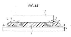
- a protruded terminal for connection (hereinafter called a bump) b is formed on the bottom electrode (not shown) of a semiconductor chip a and after the bump b and an electrode area d of a wiring pattern on a circuit board c are positioned, both are connected via joining material e such as solder and conductive paste.
- a problem is pointed out such that the manufacturing cost is increased because (1) a process for supplying and hardening the joining material e for connecting the bump b and the electrode area d of the wiring pattern is complex, (2) an insulating resin f called underfill is filled between the chip a and the board c so as to seal a bump connection portion between the bump b and the electrode area d and thereby to acquire the reliability in the moisture-proof of the bump connected part and strength for mounting the semiconductor chip and (3) a process for filling and hardening the insulating resin f to be underfill is required.
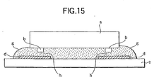
- FIG. 15 Another example of the flip-chip connection method (a second related art type method) is shown in Fig. 15.
- the second related art type method is proposed to solve the problem of the first related art type method and a bare semiconductor chip is mounted on a circuit board using an anisotropic conductive sheet proposed in Japanese Patent No. 2586154 .
- an anisotropic conductive sheet g in which conductive particulates are dispersed in thermoplastic or thermosetting resin is put between a bare semiconductor chip a and a circuit board c, and the resin is made to flow by thermocompression bonding, so that electric connection in the direction of the thickness is acquired by conductive particulates h put between a bump b and an electrode area d of the wiring pattern.
- the anisotropic conductive sheet g is relatively high-priced
- the anisotropic conductive sheet cannot be used for a board without heat resistance because the high temperature of 200°C or more is required for hardening the sheet
- it takes 10 to 20 seconds to harden the resin though it is a relatively short time and it is difficult to further simplify and speed up the process
- the reliability of connection is low because electric connection between the bump and the wiring pattern depends upon the contact of conductive particulates dispersed in the resin.
- the invention is made to solve the problems in the related art type flip-chip connection method and the object is to provide a method of mounting semiconductor chip by a flip-chip connection method in which a semiconductor chip can be mounted on a circuit board promptly, electrically and mechanically securely and further at a low cost.
- Another object of the invention is to provide a circuit board for flip-chip connection suitable for the above-mentioned mounting method.
- further another obj ect of the invention is to provide a method of manufacturing a circuit board for flip-chip connection in which the above-mentioned circuit board can be manufactured simply and at a low cost.
- furthermore another object of the invention is to provide an electromagnetic wave readable data carrier and a method of manufacturing the same in which an electromagnetic wave readable data carrier that functions as a flight tag, a label for physical distribution management, a ticket for an unmanned wicket and others can be produced at a low cost in a mass.
- further another object of the invention is to provide an electronic component module for an electromagnetic wave readable data carrier.
- a method of mounting a semiconductor chip according to the invention is provided with a process for pushing a melted thermoplastic resin coat aside by pressing a bump of a bare semiconductor chip on the melted thermoplastic resin coat applying an ultrasonic wave in a state in which the thermoplastic resin coat covering an electrode area on a wiring pattern is heated and melted and touching the bump and the electrode area, a process for bonding the bump and the electrode area by continuously applying an ultrasonic wave in a state in which the bump and the electrode area are touched and a process for cooling and solidifying the melted thermoplastic resin and bonding the body of the bare semiconductor chip on a circuit board.
- thermoplastic resin coat covering an electrode area on a wiring pattern is heated and melted
- a thermoplastic resin coat is formed beforehand in an electrode area on a wiring pattern of a circuit board used in the invention.
- This coat may also cover only an electrode area of a wiring pattern and may also cover the overall surface of a wiring pattern.
- an electrode area on a wiring pattern described above means a fixed small area on a wiring pattern including a position for a terminal of an electronic component and others to be connected. In this electrode area, a part generally called a land and others on the wiring pattern is included.
- thermoplastic resin described above has a satisfactory characteristic as an adhesive.
- action and effect are acquired that (1) secure electric conduction is acquired because the junction of the bump and the electrode area is diffused junction by an ultrasonic wave, (2) moisture-proof is satisfactory because the junction is sealed with resin, (3) mechanical mounting strength to pulling and others is high because the semiconductor chip and the circuit board are bonded when the thermoplastic resin is hardened, (4) electric conduction and mechanical bonding are simultaneously enabled in a short time, (5) the manufacturing cost is low because a process for special sealing and bonding and bonding material are not required and (6) the surface of the board is nevermore sticky than required in heating because no thermoplastic resin coat exists in a part in which the surface of the board is exposed.
- the overall surface of the wiring pattern of the circuit board for flip-chip connection according to the invention is covered with a thermoplastic resin coat.
- thermoplastic resin coat in case the circuit board described above is used for the mounting method described above, sealed structure satisfactory in moisture-proof and bonded structure high in tensile strength are acquired.
- thermoplastic resin is used for an etching mask used when the wiring pattern is formed by etching processing.
- thermoplastic resin coat covering the overall surface of a conductive pattern as it is, a special coat formation process is not required and much labor is not required, and therefore the manufacture at a low cost can be realized.
- the body of a data carrier in which a curled conductive pattern composing an antenna coil is held on thin or sheet insulating base material and an electronic component module in which a bare semiconductor chip composing a send and receive circuit, a memory and others is mounted on a wiring pattern of a thin or sheet circuit board are integrated.
- a process for manufacturing the electronic component module in which the bare semiconductor chip is mounted on the wiring pattern of the thin or sheet circuit board is mainly characteristic.
- a subprocess for pushing a melted thermoplastic resin coat aside by pressing a bump of the bare semiconductor chip on the melted thermoplastic resin coat applying an ultrasonic wave in a state in which the thermoplastic resin coat covering the electrode area on the wiring pattern is heated and melted and touching the bump and an electrode area a subprocess for bonding the bump and the electrode area by continuously applying an ultrasonic wave in a state in which the bump and the electrode area are touched and a subprocess for cooling and solidifying the melted thermoplastic resin and bonding the body of the bare semiconductor chip on the circuit board are included.
- the electromagnetic wave readable data carrier that functions as a flight tag, a label for physical distribution management, a ticket for an unmanned wicket and others can be produced at a low cost in a mass owing to action and effect that (1) secure electric conduction is acquired because the junction of the bump and the electrode area is diffused junction by an ultrasonic wave, (2) moisture-proof is satisfactory because the junction is sealed with resin, (3) mechanical mounting strength to pulling and others is high because the semiconductor chip and the circuit board are bonded when the thermoplastic resin is hardened, (4) electric conduction and mechanical bonding are simultaneously enabled in a short time, (5) the manufacturing cost is low because a process for special sealing and bonding and bonding material are not required and (6) the surface of the board is never more sticky than required in heating because no thermoplastic resin coat exists in a part in which the surface of the board is exposed.
- thermoplastic resin coat the overall surface of a wiring pattern of a circuit board used in the manufacturing process of the electronic component module according to the invention is covered with a thermoplastic resin coat.
- thermoplastic resin coat As the overall surface of the wiring pattern is covered with the thermoplastic resin coat in case the above-mentioned circuit board is used in the electronic component module manufacturing process, sealed structure satisfactory in moisture-proof and bonded structure high in tensile strength are acquired.
- thermoplastic resin is used as an etching mask used when a wiring pattern is formed by etching processing.
- the etching mask used in the etching processing for forming the wiring pattern becomes a thermoplastic resin coat covering the overall surface of a conductive pattern as it is, a special coat formation process is not required and much labor is not required, and therefore the manufacture at a low costcan be realized.
- the body of a data carrier in which a metallic foil pattern composing an antenna coil is heldon thin resin base material, and an electronic component module in which a bare semiconductor chip composing a send and receive circuit, a memory and others is mounted on a aluminum foil wiring pattern on the surface of thin resin base material are integrated.
- the electromagnetic wave readable data carrier manufacturing method a process for manufacturing the electronic component module in which the bare semiconductor chip is mounted on the aluminum foil wiring pattern on the surface of the thin resin base material is mainly characteristic.
- the overall surface of the aluminum foil wiring pattern of the circuit board according to the invention is covered with a thermoplastic resin coat.
- thermoplastic resin is used as an etching mask used when the aluminum foil wiring pattern is formed by etching processing.
- thermoplastic rein polyolefin resin or polyester resin is used.
- Action and effect can be desired by using such resin such that the resistance to a chemical satisfactory for an etching mask, and satisfactory junction strength between a metallic bump on the side of the semiconductor chip and a metallic electrode area on the side of the wiring pattern are acquired. That is, polyolefin resin is provided with satisfactory resistance to alkaline etchant such as NaOH or polyester resin is provided with satisfactory resistance to acid etchant such as FeCl 2 . In addition, these resins are also excellent in an adhesive property.
- an electronic component module for an electromagnetic wave readable data carrier comprises: a circuit board having a wiring pattern with an electrode area and a thermoplastic resin coat covering the electrode area of the wiring pattern; and a semiconductor chip mounted on the circuit board, said semiconductor chip having a bump at a side of the circuit board thereof.
- the bump of the semiconductor chip penetrates the thermoplastic resin coat and directly bonds with the electrode area of the wiring pattern.
- an electromagnetic wave readable data carrier comprises: a body of a data carrier including an insulating base material and a conductive pattern held on the insulating base material; and an electronic component module including a circuit board and a semiconductor chip mounted on the circuit board, said circuit board having a wiring pattern with an electrode area and a thermoplastic resin coat covering the electrode area of the wiring pattern, said semiconductor chip having a bump at a side of the circuit board thereof, the bump of the semiconductor chip penetrating the thermoplastic resin coat and directly bonding with the electrode area of the wiring pattern, wherein said electronic component module is manufactured by a method comprising: heating and melting the thermoplastic resin coat of said circuit board; pressing the bump of said semiconductor chip on the thus melted thermoplastic resin coat while applying an ultrasonic wave to the bump so that the bump penetrates the melted thermoplastic resin coat and brings into contact with electrode area; bonding the bump and the electrode area by continuously applying the ultrasonic wave to the bump bringing into contacted with the electrode area; and cooling and solidifying the melted thermo
- the semiconductor chip mounting method is provided with: 1) a process for pushing a heated and melted thermoplastic resin coat covering an electrode area on a wiring pattern aside by pressing a bump of a bare semiconductor chip on the melted thermoplastic resin coat applying an ultrasonic wave so as to bring the bump into contact with the electrode area; 2) a process for bonding the bump and the electrode area by continuously applying an ultrasonic wave in a state in which the bump and the electrode area are in contact; and 3) a process for cooling and solidifying the melted thermoplastic resin and bonding the body of the bare semiconductor chip on a circuit board.
- FIG. 1A-E An outline of a series of processes including such a mounting method is shown in a process drawing shown in Figs. 1A-E.
- a metallic foil lamination manufacturing process A
- an etching mask printing process B
- an etching process for forming a wiring pattern C
- an ultrasonic mounting process D
- a bonding process E
- an Al-PET lamination 1 which is original material of a thin circuit board is manufactured.
- the Al-PET lamination 1 is manufactured in a process for laminating hard aluminum foil 3 having the thickness of 35 ⁇ m on the single side (the upper surface in Fig. 1A) of a PET film 2 having the thickness of 25 ⁇ m via an urethane adhesive, and bonding them thermally under a condition of the temperature of 150°C and the pressure of 5 kg/cm 2 .
- an etching resist pattern 4 in the shape of a required wiring pattern is formed on the surface of the hard aluminum foil 3 of the Al-PET lamination 1.
- the resist pattern 4 is formed by applying a polyolefin thermoplastic resin adhesive, which is melted at the temperature of approximately 150°C, on the surface of the hard aluminum foil 3 by approximately 4 to 6 ⁇ m in thickness by a method such as gravure. It is desirable that this thickness is varied according to the size and the shape of a bump of a mounted bare chip.
- a wiring pattern 6 composed of the hard aluminum foil 3 is formed by removing an aluminum foil part 5 exposed from the etching resist pattern 4 by well-known etching process.
- the wiring pattern 6 is formed by exposing the aluminum foil part 5 exposed from the etching resist pattern 4 to NaOH (120 g/l) used as etchant under a condition of the temperature of 50°C.
- the wiring pattern 6 composed of the hard aluminum foil 3 appears on the surface of a circuit board 7 acquired in this etching process.
- the overall surface of the wiring pattern 6 is covered with the polyolefin thermoplastic resin adhesive used for the etching resist pattern (an etching mask) 4.
- the surface of at least an electrode area (an area to be connected with a bump of a bare semiconductor chip described later) of the wiring pattern 6 is covered with a thermoplastic resin coat 4a.
- a bare semiconductor chip 8 is mounted on the circuit board 7 applying an ultrasonic wave.
- This process includes: 1) a subprocess (a first subprocess) for pushing the melted thermoplastic resin coat 4a aside by pressing a bump 9 of the bare semiconductor chip 8 on the melted thermoplastic resin coat 4a in a state in which the thermoplastic resin coat 4a covering an electrode area 10 on the wiring pattern 6 is heated and melted applying an ultrasonic wave so as to bring the bump 9 into contact with the electrode area 10 ; and 2) a subprocess (a second subprocess) for bonding the bump 9 and the electrode area 10 in a state in which the bump 9 and the electrode area 10 are contacted with each other by continuously applying an ultrasonic wave.
- the bare semiconductor chip 8 is composed as a so-called surface mounting-type component. That is, the bare semiconductor chip 8 has a body which has 150 ⁇ m thick and the bump 9 which is a metallic terminal for connection and protruded from the bottom of the bare semiconductor chip 8..
- the bump (made of gold for example) 9 is pressed on the thermoplastic resin coat 4a which is melted by heating at 150°C in a state in which an ultrasonic wave is applied. Then, the melted thermoplastic resin coat 4a is pushed aside and removed from the position of the end of the bump 9 by the ultrasonic vibration of the bump 9. Further, an oxide layer and others on the surface of the aluminum foil wiring pattern 6 are also mechanically removed by the vibration.
- the bump 9 and the electrode area 10 are contacted with each other.
- the bump 9 and the electrode area 10 of the wiring pattern 6 are further heated by frictional heat by the vibration, a metallic fused part in which atoms of gold are diffused in the aluminum foil is formed and the bonding of both by an ultrasonic wave is completed.
- the first and second subprocesses are completedby applying ultrasonic vibration of the frequency of 63 kHz by approximately a few seconds under the pressure of 0.2 kg/mm 2 for example after the bare semiconductor chip 8 is arranged in a predetermined position.
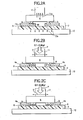
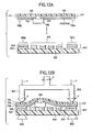
- a process drawing shown in Figs. 2A-C The details of the ultrasonic mounting process are shown in a process drawing shown in Figs. 2A-C.
- a positioning process shown in Fig. 2A in a state in which an ultrasonic horn 11 and an anvil 12 used as a heater table respectively provided with a vacuum attraction function are arranged opposite, the bare chip 8 is attracted to the ultrasonic horn 11 as shown by an arrow 11a and the circuit board 7 is attracted to the anvil 12 as shown by an arrow 12a.
- the bump 9 on the side of the bare chip 8 and the electrode area 10 of the wiring pattern 6 on the side of the circuit board 7 are positioned, relatively moving the ultrasonic horn 11 and the anvil 12 in a horizontal direction.
- the circuit board 7 is heated up to 150°C by the anvil 12.
- thermoplastic resin adhesive shown in Fig. 2B
- the melted thermoplastic resin coat 4a is pushed aside by pressing the bump 9 of the bare chip 8 on the thermoplastic resin adhesive (the thermoplastic resin coat) 4a in a heated and melted state by applying pressure (0.1 to 0.3 kgf) as shown by an arrow P, as applying ultrasonic vibration (63.5 kHz, 2W) as shown by an arrow v by the ultrasonic horn 11 and the anvil 12. Therefore, the bump 9 and the electrode area 10 are contacted with each other.
- thermoplastic resin coat 4a is hardened again by natural cooling or forced cooling by removing the heat of 150°C applied to the circuit board. Therefore, the bare semiconductor chip 8 and the wiring pattern 6 are bonded. That is, the thermoplastic resin coat 4a in a melted state filled between the bottom of the bare semiconductor chip 8 and the circuit board 7 is cooled and solidified, and the bare semiconductor chip 8 and the circuit board 7 are firmly bonded and fixed.
- the mounted structure completed in the processes (A) to (E) is shown in Fig. 3.
- action and effect are acquired such that (1) sure electric conduction is acquired because the bump 9 and the electrode area 10 are bonded by diffused junction by an ultrasonic wave, (2) the moisture-proof is satisfactory because a junction between the bump 9 and the electrode area 10 is sealed with resin, (3) the mechanical strength of mounting for pulling and others is high because the semiconductor chip 8 and the circuit board 7 are bonded when the thermoplastic resin coat 4a is hardened, (4) electric conduction and mechanical coupling are simultaneously enabled in a short time, (5) the manufacturing cost is particularly low because special processes from sealing to bonding and adhesive material are not required and (6) the surface of the board is never more sticky than required in heating because no thermoplastic resin coat exists in a part in which the surface of the board is exposed.
- the strength of bonding between the bare semiconductor chip 8 and the wiring pattern 6 in the case of the mounting method using the resin coat in this embodiment is shown in Fig. 4 in comparison with a case using only ultrasonic bonding.
- Fig. 4 in the case of the mounting method according to the invention, the double to triple strength of bonding is acquired, compared with the case of only ultrasonic bonding. It need scarcely be said that this is because the semiconductor chip 8 and the circuit board 7 are bonded when the thermoplastic resin coat 4a is hardened.
- the PET film 2 is used for resin base material composing the lamination 1, however, a polyimide film and others can be also used in place of the PET film.
- polyester thermoplastic resin can be also used in place of the polyolefin resin.
- FeCl 2 is used for etchant.
- the overall surface of the wiring pattern 6 is covered with the thermoplastic resin coat 4a and the circuit board can be generalized as a circuit board for flip-chip connection.
- thermoplastic resin coat 4a located in the vicinity of the electrode area 10 on the wiring pattern 6 mainly contributes to sealing the ultrasonic junction, while the thermoplastic resin coat 4a located in a part except the electrode area contributes to the bonding of the body of the semiconductor chip 8 and the circuit board 7.
- thermoplastic resin is used for an etching mask used when the wiring pattern is formed by etching processing and the circuit board manufacturing method can be generalized as a method of manufacturing a circuit board for flip-chip connection.
- the material of the etching mask used in etching processing for forming the wiring pattern becomes the thermoplastic resin coat covering the overall surface of a conductive pattern as it is, a coat formation process is not required and labor is not required. Therefore the manufacture at a low cost is realized.
- This data carrier functions as a flight tag, a label for physical distribution management, a ticket for an unmanned wicket and others and can read an electromagnetic wave.
- This data carrier is composed by integrating the body of the data carrier with an electronic component.
- a metallic foil pattern composing an antenna coil is held on thin resin base material.
- a bare semiconductor chip composing a send and receive circuit, a memory and others is mounted on an aluminum foil wiring pattern on the surface of the thin resin base material.
- the data carrier DC is provided with the body of the data carrier 100 and an electronic component module 200.
- a copper foil curled conductive pattern (equivalent to an antenna coil) 102 having the thickness of 10 ⁇ m is held on the single side of polyethylene terephthalate (PET) base material 101 having the thickness of 25 ⁇ m.
- PET polyethylene terephthalate
- bare chip IC 202 is mounted on the lower side in Fig. 5 of a glass epoxy piece 201 having the thickness of 70 ⁇ m.
- the electronic component module 200 is mounted on the body of the data carrier 100 so that the piece 201 crosses an orbital conductive flux 102a composing the curled conductive pattern 102. Electric connection of the electronic component module 200 with the curled conductive pattern 102 is performed in a terminal pad on the inner side 103 and in a terminal pad on the outer side 104 of the curled conductive pattern 102.
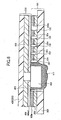
- FIG. 6 An example of the structure in which the electronic component module 200 is mounted is shown in an enlarged sectional view in Fig. 6.
- a method of manufacturing the body of the data carrier 100 and the electronic component module 200 respectively shown in Figs. 5 and 6 will be sequentially described in detail below.
- FIGs. 7A-E An example of the manufacturing process of the curled conductive pattern 102 composing an antenna coil is shown in Figs. 7A-E. Referring to Figs. 7A-E, a process when the curled conductive pattern 102 to be an antenna coil is formed on the single side of the PET film base material 101 will be described.
- a Cu-PET lamination 301 is prepared.
- copper foil 303 having the thickness of 10 ⁇ m is laminated on the single side of a PET film 302 having the thickness of 25 ⁇ m via an urethane adhesive. Then they is thermically bonded under a condition of the temperature of 150°C and the pressure of 5 kg/cm 2 .
- the Cu-PET lamination 301 in which the cupper foil 303 is bonded on the surface of the PET film 302 is completed.
- a curled etching resist pattern 304 is formed on the surface of the copper foil 303 of the Cu-PET lamination 301. That is, insulating etching resist ink is printed on the copper foil 303 using an offset printing method for example so that the insulating etching resist ink has a curled shape having the number of turns, the width, the pitch and the inside and outside circumferences for acquiring an L value and a Q value respectively required for the characteristics of a coil.
- a type hardened by heat or an active energy beam is used.
- the active energy beam ultraviolet rays or an electron beam is used. In case ultraviolet rays are used, the resist ink including a photopolymerization agent and is used.
- conductive etching resist patterns 305a and 305b (103 and 104 in Fig. 5) in the shape of a required electrode are formed by conductive ink in a position for electric connection with the electrode of the electronic component module 200 on the surface of the copper foil 303 of the Cu-PET lamination 301.
- These resist patterns 305a and 305b are formed by offset printing as in the above-mentioned process.
- resist ink a thermosetting conductive adhesive hardened by heat treatment at 120°C for approximately 20 minutes is used.
- a screen printing method generally performed may be also used for the printing of conductive ink in this process.
- ink material a chemical acquired by adding a photopolymerization agent to the mixture of Ag particles and an thermoplastic adhesive for example or solder paste and others may be also used.
- a copper foil part 306 exposed from the etching resist patterns 304, 305a and 305b is removed by executing well-known etching and a curled conductive pattern (102 in Fig. 5) to be an antenna coil is formed.
- FeCl 2 120 g/l
- the copper foil 303 is removed.
- an electronic component cannot be mounted on a circuit, that is, on a curled pattern composing an antenna coil.
- the conductive resist patterns 305a and 305b are provided and etching resist is not required to be removed by mounting an electronic component in this position. That is, a process for peeling the etching resist can be omitted by the invention. Further, there is also effect that the etching resist 304 formed by insulating ink also functions as an insulating protective layer on the surface of the copper foil circuit pattern.
- a transparent hole 307 into which a convex portion(a potting part 411) described later of the electronic component module can be inserted is formed by a press process.
- FIGs. 8A-E an example of the manufacturing process of the electronic component module 200 is shown in Figs. 8A-E.
- the contents shown in Figs. 8A-E are the same as the contents described above referring to Figs. 1A-E except that a bare chip 408 is sealed with resin in the potting part 411 in a final process and conductive resist 412 is arranged in an electrode part for connection with the body of the data carrier 100.
- an Al-PET lamination 401 which is the base material of a thin circuit board is manufactured.
- the Al-PET lamination 401 is manufactured in a process for laminating hard aluminum foil 403 having the thickness of 35 ⁇ m on the single side (the upper surface in Fig. 8A) of a PET film 402 having the thickness of 25 ⁇ m via an urethane adhesive and thermically bonding them under a condition of the temperature of 150°C and the pressure of 5 kg/cm 2 .
- an etching resist pattern 404 in the shape of a required wiring pattern is formed on the surface of the hardaluminum foil 403 of theAl-PET lamination 401.
- the resist pattern 404 is formed by applying a polyolefin thermoplastic resin adhesive, which is melted at the temperature of approximately 150°C, on the surface of the hard aluminum foil 403 by approximately 4 to 6 ⁇ m in thickness by a method such as gravure. It is desirable that the applied thickness is adjusted according to the size and the shape of a bump of a mounted bare chip.
- conductive etching resist patterns 412a and 412b in the shape of a required electrode pattern are arranged in each connection with terminal pads 305a and 305b of the body of the data carrier 100.
- These resist patterns 412a and 412b are formed by offset printing as in the above-mentioned process.
- resist ink a thermosetting conductive adhesive hardened by heat treatment at 120°C for approximately 20 minutes is used.
- screen printing generally performed may be also used.
- ink material a chemical in which a photopolymerization agent is added to the mixture of Ag particles and an thermoplastic adhesive for example or solder paste and others may be also used.
- a wiring pattern 406 made of hard aluminum foil 403 is formed by removing an aluminum foil part 405 exposed from the etching resist pattern 404 by well-known etching processing.
- this wiring pattern 406 is formed by exposing the aluminum foil part 405 exposed from the etching resist pattern 404 to NaOH (120 g/l) which is etchant under a condition of the temperature of 50°C.
- the wiring pattern 406 made of hard aluminum foil 403 appears on the surface of a circuit board 407 acquired in this etching process.
- the overall surface of the wiring pattern 406 is covered with the polyolefin thermoplastic resin adhesive used for the etching resist pattern (an etching mask) 404.
- the surface of at least the electrode area (an area to be connected with the bump of the bare semiconductor chip described later) of this wiring pattern 406 is covered with a thermoplastic resin coat 404a.
- the bare semiconductor chip 408 is mounted on the circuit board 407 applying an ultrasonic wave.
- This process includes: 1) a first subprocess for pushing the melted thermoplastic resin coat 404a aside by pressing a bump 409 of the bare semiconductor chip 408 on the melted thermoplastic resin coat 404a applying an ultrasonic wave in a state in which the thermoplastic resin coat 404a covering an electrode area 410 on the wiring pattern 406 is heated and melted so as to bring the bump 409 into contact with the electrode area 410 and 2) a second subprocess for bonding the bump 409 and the electrode area 410 by continuously applying an ultrasonic wave in a state in which the bump 409 and the electrode area 410 are contacted with each other.
- the bare semiconductor chip 408 is composed as a so-called surface mounting-type component. That is, the bare semiconductor chip 408 has a body which is 150 ⁇ m thick and the bump 409 which is a metallic terminal for connection and protruded form the bottom of the bare semiconductor 408.
- the bump (made of gold for example) 409 is pressed on the thermoplastic resin coat 404a which is melted by heating at 150°C applying ultrasonic vibration. Then, the melted thermoplastic resin coat 404a is pushed aside and removed from the end position of the bump 409 by the ultrasonic vibration of the bump 409. Further, an oxide layer and others on the surface of the aluminum foil wiring pattern 406 are also mechanically removed by the vibration.
- the bump 409 and the electrode area 410 are contacted with each other.
- the bump 409 and the electrode area 410 of the wiring pattern 406 are heated by frictional heat by the vibration further, a metallic fused part in which atoms of gold are diffused in the aluminum foil is formed and the ultrasonic junction of both is completed.
- the first and second subprocesses are completedby applying ultrasonic vibration at the frequency of 63 kHz for approximately a few seconds under the pressure of 0.2 kg/mm 2 for example after the bare semiconductor chip 408 is arranged in a predetermined position.
- the melted thermoplastic resin coat 404a is rehardened by natural cooling or forced cooling by removing the heat of 150°C applied to the circuit board, and the body of the bare semiconductor chip 408 and the wiring pattern 406 are bonded. That is, the melted thermoplastic resin coat 404a filled between the bottom of the bare semiconductor chip 408 and the circuit board 407 is cooled and solidified, and the bare semiconductor chip 408 and the circuitboard 407 are firmly bonded and fixed. Afterward, the bare semiconductor chip 408 is sealed with resin by a well-known method if necessary and the potting part 411 is formed.
- the electronic component module 200 is mounted on the body of the data carrier 100 so that the electronic component mounted side of the electronic component module 200 and the conductive pattern formation side of the body of the data carrier 100 are opposite, and the electronic component module 200 crosses the orbital conductive flux 102a composing the curled conductive pattern 102.
- the potting part 411 covering the bare chip 408 which is an electronic component is inserted into the hole 307 made on the side of the body of the data carrier 100.
- the conductive resist areas 412a and 412b to be electrode areas of a pair of aluminum foil areas 406 connected to the bumps 409 of the bare chip 408 on the side of the electronic component module 200 are respectively located over a pair of conductive resist patterns 305a and 305b on the side of the body of the data carrier 100. That is, the copper foil areas 406 on the side of the electronic component module 200 and the conductive resist patterns 305a and 305b on the side of the body of the data carrier 100 are respectively opposite via the conductive resist areas 412.
- indentators 501a and 501b heated up to 160°C are pressed particularly on a pair of conductive resist patterns 305a and 305b at the pressure of 21.7 kg for 20 seconds from over the electronic component module 200.
- the conductive resist pattern which is a thermoplastic adhesive coat is locally softened and melted, and the conductive resist areas 412a and 412b that respectively conduct to the terminal areas 406 of the electronic component module 200 and the conductive resist patterns 305a and 305b on the side of the body of the data carrier 100 are respectively bonded and fixed.
- the thermoplastic resin coat 404a can be utilized for the junction of the electronic component module 200 and the body of the data carrier 100 with the thermoplastic resin coat keeping insulation.
- the etching resist 304 on the surface of the curled conductive pattern 102 is left as insulating material. Therefore, a wiring pattern (not shown) on the insulating base material piece 402 (201) of the electronic component module 200 also functions as a jumper member mating the inside and the outside of the curled conductive pattern 102. As a result, the curled conductive pattern 102 and the bare chip 408 can be electrically connected without using a jumper member, a back wiring pattern and others as in related art type structure.
- This data carrier also functions as a flight tag, a label for physical distribution management, a ticket for an unmanned wicket and others and can also read an electromagnetic wave.
- This data carrier is also composed by integrating the body of a data carrier with electronic component module on the surface of the thin resin base material as in the embodiment described referring to Fig. 5.
- a metallic foil pattern composing an antenna coil is held on thin resin base material.
- a bare semiconductor chip composing a send and receive circuit, a memory and others is mounted on an aluminum foil wiring pattern.
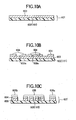
- FIG. 10A-C An example of the manufacturing process of the curled conductive pattern 102 shown in Fig. 5 composing an antenna coil is shown in Figs. 10A-C.
- Figs. 10A-C processes when the curled conductive pattern 102 shown in Fig. 5 to be an antenna coil is formed on the single side of the PET film base material 101 as shown in Fig. 5 will be described below.
- Cu-PET lamination base material 601 is prepared.
- copper foil having the thickness of 10 ⁇ m is laminated on the single side of a PET film having the thickness of 25 ⁇ m via an urethane adhesive and is thermically bonded under a condition of the temperature of 150°C and the pressure of 5 kg/cm 2 .
- the Cu-PET lamination 601 in which the cupper foil 603 is bonded on the surface of the PET film 602 (101) is completed.
- a curled etching resist pattern 604 and an etching resist pattern 604 in the shape of a terminal are formed on the surface of the copper foil 603 of the Cu-PET lamination 601. That is, insulating etching resist ink is printed on the copper foil using an offset printing method for example so that the insulating etching resist ink has a curled shape having the number of turns, the width, the pitch and the inside and outside circumferences for acquiring an L value and a Q value respectively required for the characteristics of a coil.
- a type hardened by heat or an active energy beam is used.
- the active energy beam ultraviolet rays or an electron beam is used and in case ultraviolet rays are used.
- the resist ink including a photopolymerization agent is used.
- a curled conductive pattern 605 and terminal pads 606a and 606b on the inside and outside circumferences respectively composing an antenna coil are formed by removing a copper foil part 603a exposed from the etching resist pattern 604 formed in the above-mentioned process by well-known etching.
- FeCl 2 120 g/l is used for etchant under a condition of the temperature of 50°C and the required copper foil (Cu) is removed.
- the insulating etching resist 604 formed in the process B is removed, an electronic component cannot be mounted on a circuit, that is, on a coil.
- the insulating resist 604 is not required to be removed. That is, according to the invention, a process for peeling the etching resist 604 canbeomitted. Further, effect is acquired such that the etching resist 604 can be used for an insulating protective layer on the surface of the copper conductive pattern 605.
- anAl-PET lamination 701 which is original material of a thin circuit board is manufactured.
- the Al-PET lamination 701 is manufactured in a process for laminating hard aluminum foil 703 having the thickness of 35 ⁇ m on the single side (the upper surface in Figs. 11 A-E) of a PET film 702 having the thickness of 25 ⁇ m via an urethane adhesive and bonding them thermally under a condition of the temperature of 150°C and the pressure of 5 kg/cm 2 .
- an etching resist pattern 704 in the shape of a required wiring pattern is formed on the surface of the hard aluminum foil 703 of theAl-PET lamination 701.
- the resist pattern 704 is formed by applying a polyolefin thermoplastic resin adhesive, which is melted at the temperature of approximately 150°C, on the surface of the hard aluminum foil 703 by approximately 4 to 6 ⁇ m in thickness by a method such as gravure. It is desirable that this thickness is varied according to the size and the shape of a bump of a mounted bare chip.
- a wiring pattern 706 made of the hard aluminum foil 703 is formed by removing an aluminum foil part 705 exposed from the etching resist pattern 704 by well-known etching processing.
- the wiring pattern 706 is formed by exposing the aluminum foil part 705 exposed from the etching resist pattern 704 to NaOH (120 g/l) which is etchant under a condition of the temperature of 50°C.
- the wiring pattern 706 made of the hard aluminum foil 703 is formed on the surface of a circuit board 707 acquired in this etching process.
- the overall surface of the wiring pattern 706 is covered with the polyolefin thermoplastic resin adhesive used for the etching resist pattern (an etching mask) 704.
- the surface of at least an electrode area (an area to be connected with a bump of a bare semiconductor chip described later) of the wiring pattern 706 is covered with a thermoplastic resin coat 704a.
- a bare semiconductor chip 708 is mounted on the circuit board 707 applying an ultrasonic wave.
- This process includes: 1) a subprocess (a first subprocess) for pushing the melted thermoplastic resin coat 704a aside by pressing a bump 709 of the bare semiconductor chip 708 on the melted thermoplastic resin coat 704a in a state in which the thermoplastic resin coat 704a covering an electrode area 710 on the wiring pattern 706 is heated and melted applying an ultrasonic wave so as to bring the bump 709 into contact with the electrode area 710; and 2) a subprocess (a second subprocess) for bonding the bump 709 and the electrode area 710 in a state in which the bump 709 and the electrode area 710 are contacted with each other by continuously applying an ultrasonic wave.
- the bare semiconductor chip 708 is composed as a so-called surface mounting-type component. That is, the bare semiconductor chip 708 has a body which is 150 ⁇ m thick and the bump 709 which is a metallic terminal for connection and protruded form the bottom of the bare semiconductor chip 708.
- the bump (made of gold for example) 709 is pressed on the thermoplastic resin coat 704a which is melted by heating at 150°C applying an ultrasonic wave. Then, the melted thermoplastic resin coat 704a is pushed aside and removed from the position of the end of the bump 709 by the ultrasonic vibration of the bump 709. Further, an oxide layer and others on the surface of the aluminum foil wiring pattern 706 are also mechanically removed by the vibration.
- the bump 709 and the electrode area 710 are contacted with each other.
- the bump 709 and the electrode area 710 of the wiring pattern 706 are further heated by frictional heat by the vibration, a metallic fused part in which atoms of gold are diffused in the aluminum foil is formed and the bonding of both by an ultrasonic wave is completed.
- the first and second subprocesses are completedby applying ultrasonic vibration of the frequency of 63 kHz by approximately a few seconds under the pressure of 0.2 kg/mm 2 for example after the bare semiconductor chip 708 is arranged in a predetermined position.
- the melted thermoplastic resin coat 704a is hardened again by natural cooling or forced cooling by removing the heat of 150°C applied to the circuit board, and the body of the bare semiconductor chip 708 and the wiring pattern 706 are bonded. That is, the thermoplastic resin coat 704a in a melted state filled between the bottom of the bare semiconductor chip 708 and the circuit board 707 is cooled and solidified, and the bare semiconductor chip 708 and the circuit board 707 are firmly bonded and fixed. Afterward, the bare semiconductor chip 708 is sealed with resin by a well-known method if necessary and a potting part 711 is formed. As a result, an electronic component module 707 is completed.
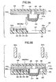
- a process for mounting the electronic component module 707 on the data carrier 607 and electrically connecting with an antenna coil will be described. This process is executed using ultrasonic welding technology.
- the electronic component module 707 is mounted on the body of the data carrier 607 in a matched state that parts to be bonded 708a and 708b on the side of the electronic component and terminal pads 606a and 606b which are parts to be bonded on the side of the body of the data carrier are opposite.
- indentators 801 and 802 that fall integrally are pressed over the parts to be bonded 708a and 708b of the electronic component module 707 by time T (approximately 0.5 second) applying the ultrasonic vibration of applied pressure P (0.2 kg/mm 2 ) and a frequency V (40 kHz).
- Reference numbers 803 and 804 denote anvils arranged opposite to the indentators 801 and 802.
- welding is caused by bringing atoms at distance (a few angstrom ( ⁇ )) at which attraction is exerted between atoms on the surfaces of metals to be bonded and contacting with the surfaces with atoms on the overall surfaces orderly arrayed.
- ⁇ angstrom
- the approach of clean metallic atoms under it is prevented and sufficient bonding power is not caused.
- the terminal of the electronic component module and the terminal on the side of the antenna coil are bonded and fixed by removing a metallic superficial layer by ultrasonic vibration by the above-mentioned method, further activating the vibration of atoms and diffusing atoms.
- this method is based upon a principle that bonding is realized by removing a metallic superficial layer by ultrasonic vibration as described above and even if the bonding process is executed in a state in which insulating etching resist 704 formed on the terminal pads 606a and 606b of the conductive pattern is not peeled as shown in the process (B) in Fig. 12B, a sufficient electric and mechanical bonding characteristic is acquired between the side of the electronic component module 707 and the side of the body of the data carrier 607.
- the thin data carrier DC (see Fig. 5) according to the invention is completed by the processes described above.
- the plastic flow of metal is locally caused corresponding to the protruded part by providing multiple irregularities corresponding to the shape of the fused part to the end face of the anvils 803 and 804 opposite to the indentators 801 and 802 for example and in the meantime, adjusting the pressing time of the indentators 801 and 802 and resin layers exposed from a part from which a metallic layer is removed can be fused by ultrasonic vibration.
- the mechanical bonding strength of the electronic component module is particularly enhanced in case such fusion of metal and the fusion of resin are both used, the data carrier is effective when it is often roughly handled as a flight tag and a label for physical distribution management.
- the thin data carrier completed as described above uses an electromagnetic field as a read medium, it can securely read data stored in the semiconductor chip apart by the distance of 100 to 1000 mm without being restricted by distance and a direction in reading so much, concretely without being restricted by the direction of reading.
- the result of the moisture-proof test (at the temperature of 85°C and at the humidity of 85%) of the thin data carrier manufactured in this embodiment is shown in Fig. 13.
- the variation of communication distance after 250 hours elapse in the moisture-proof test is within ⁇ 10%. It is verified that for reliability on the moisture-proof of the connection of the bump, a sufficient value is acquired.
- the semiconductor chip mounting method by the flip-chip connection method in which the semiconductor chip can be mounted on the circuit board promptly, electrically and mechanically securely and further, at a low cost can be provided.
- the electromagnetic wave readable data carrier manufacturing method in which the electromagnetic wave readable data carrier that functions as a flight tag, a label for physical distribution management, a ticket for an unmanned wicket and others can be produced at a low cost in a mass can be provided.
Landscapes
- Engineering & Computer Science (AREA)
- Manufacturing & Machinery (AREA)
- Microelectronics & Electronic Packaging (AREA)
- Wire Bonding (AREA)
- Encapsulation Of And Coatings For Semiconductor Or Solid State Devices (AREA)
Applications Claiming Priority (2)
| Application Number | Priority Date | Filing Date | Title |
|---|---|---|---|
| JP33340999A JP3451373B2 (ja) | 1999-11-24 | 1999-11-24 | 電磁波読み取り可能なデータキャリアの製造方法 |
| EP00310393A EP1104017B1 (fr) | 1999-11-24 | 2000-11-23 | Montage à puce inversée d'une puce semi-conducteur sur un panneau à circuit |
Related Parent Applications (1)
| Application Number | Title | Priority Date | Filing Date |
|---|---|---|---|
| EP00310393A Division EP1104017B1 (fr) | 1999-11-24 | 2000-11-23 | Montage à puce inversée d'une puce semi-conducteur sur un panneau à circuit |
Publications (2)
| Publication Number | Publication Date |
|---|---|
| EP1801867A2 true EP1801867A2 (fr) | 2007-06-27 |
| EP1801867A3 EP1801867A3 (fr) | 2007-08-29 |
Family
ID=18265800
Family Applications (2)
| Application Number | Title | Priority Date | Filing Date |
|---|---|---|---|
| EP00310393A Expired - Lifetime EP1104017B1 (fr) | 1999-11-24 | 2000-11-23 | Montage à puce inversée d'une puce semi-conducteur sur un panneau à circuit |
| EP07006007A Ceased EP1801867A3 (fr) | 1999-11-24 | 2000-11-23 | Procédé pour le montage d'une puce semi-conductrice, carte de circuit pour connexion par billes et son procédé de fabrication |
Family Applications Before (1)
| Application Number | Title | Priority Date | Filing Date |
|---|---|---|---|
| EP00310393A Expired - Lifetime EP1104017B1 (fr) | 1999-11-24 | 2000-11-23 | Montage à puce inversée d'une puce semi-conducteur sur un panneau à circuit |
Country Status (7)
| Country | Link |
|---|---|
| US (2) | US6406990B1 (fr) |
| EP (2) | EP1104017B1 (fr) |
| JP (1) | JP3451373B2 (fr) |
| KR (2) | KR20010070230A (fr) |
| CN (2) | CN100473255C (fr) |
| DE (1) | DE60034756T2 (fr) |
| SG (1) | SG114482A1 (fr) |
Families Citing this family (168)
| Publication number | Priority date | Publication date | Assignee | Title |
|---|---|---|---|---|
| KR100672130B1 (ko) * | 1999-07-08 | 2007-01-19 | 산스타 기켄 가부시키가이샤 | 반도체 패키지용 언더필링 재료 |
| JP3498285B2 (ja) | 1999-12-20 | 2004-02-16 | 澁谷工業株式会社 | 半導体チップの接合方法及び接合装置 |
| DE10012882C2 (de) * | 2000-03-16 | 2002-06-20 | Infineon Technologies Ag | Verfahren und Vorrichtung zur Aufbringung eines Halbleiterchips auf ein Trägerelement |
| JP3422019B2 (ja) | 2000-04-07 | 2003-06-30 | 日本電気株式会社 | Bga型半導体装置、及び、bgaの実装方法 |
| JP3491827B2 (ja) * | 2000-07-25 | 2004-01-26 | 関西日本電気株式会社 | 半導体装置及びその製造方法 |
| US6519844B1 (en) * | 2001-08-27 | 2003-02-18 | Lsi Logic Corporation | Overmold integrated circuit package |
| TWI230102B (en) * | 2002-03-27 | 2005-04-01 | Matsushita Electric Industrial Co Ltd | Component mounting method, component mounting apparatus, and ultrasonic bonding head |
| CN100524706C (zh) * | 2002-05-31 | 2009-08-05 | 富士通微电子株式会社 | 半导体器件的制造方法 |
| US6978539B2 (en) * | 2002-07-17 | 2005-12-27 | Compal Electronics, Inc. | Method for attaching an integrated circuit package to a circuit board |
| JP2004163262A (ja) * | 2002-11-13 | 2004-06-10 | Touch Panel Systems Kk | 音響波型接触検出装置 |
| JP4090329B2 (ja) * | 2002-11-13 | 2008-05-28 | タッチパネル・システムズ株式会社 | 音響波型接触検出装置 |
| JP3533665B1 (ja) * | 2002-12-17 | 2004-05-31 | オムロン株式会社 | 電子部品モジュールの製造方法、並びに電磁波読み取り可能なデータキャリアの製造方法。 |
| TW200507218A (en) * | 2003-03-31 | 2005-02-16 | North Corp | Layout circuit substrate, manufacturing method of layout circuit substrate, and circuit module |
| US8704359B2 (en) | 2003-04-01 | 2014-04-22 | Ge Embedded Electronics Oy | Method for manufacturing an electronic module and an electronic module |
| FI115601B (fi) * | 2003-04-01 | 2005-05-31 | Imbera Electronics Oy | Menetelmä elektroniikkamoduulin valmistamiseksi ja elektroniikkamoduuli |
| JP2004335916A (ja) * | 2003-05-12 | 2004-11-25 | Toshiba Corp | 半導体装置の製造方法 |
| JP4052290B2 (ja) * | 2003-08-29 | 2008-02-27 | オムロン株式会社 | 無線icタグ接合方法、無線icタグ付き物品、及び車両 |
| JP4494746B2 (ja) * | 2003-09-25 | 2010-06-30 | 浜松ホトニクス株式会社 | 半導体装置 |
| JP4351012B2 (ja) * | 2003-09-25 | 2009-10-28 | 浜松ホトニクス株式会社 | 半導体装置 |
| JP4494745B2 (ja) * | 2003-09-25 | 2010-06-30 | 浜松ホトニクス株式会社 | 半導体装置 |
| US20070075436A1 (en) * | 2003-10-06 | 2007-04-05 | Nec Corporation | Electronic device and manufacturing method of the same |
| TW200520123A (en) * | 2003-10-07 | 2005-06-16 | Matsushita Electric Industrial Co Ltd | Method for mounting semiconductor chip and semiconductor chip-mounted board |
| JP4438558B2 (ja) * | 2003-11-12 | 2010-03-24 | 株式会社日立製作所 | Rfidタグの製造方法 |
| DE10356153B4 (de) * | 2003-12-02 | 2010-01-14 | Infineon Technologies Ag | Modul für kontaktlose Chipkarten oder Identifizierungssysteme |
| JP4260617B2 (ja) * | 2003-12-24 | 2009-04-30 | 株式会社ルネサステクノロジ | 半導体装置の製造方法 |
| JP4567988B2 (ja) * | 2004-02-05 | 2010-10-27 | 株式会社日立製作所 | 紙状rfidタグおよびその製造方法 |
| JP2005275802A (ja) * | 2004-03-24 | 2005-10-06 | Omron Corp | 電波読み取り可能なデータキャリアの製造方法および該製造方法に用いる基板並びに電子部品モジュール |
| JP4251104B2 (ja) * | 2004-03-31 | 2009-04-08 | 株式会社日立製作所 | Rfidタグの製造方法 |
| TWI288885B (en) * | 2004-06-24 | 2007-10-21 | Checkpoint Systems Inc | Die attach area cut-on-fly method and apparatus |
| JP4264388B2 (ja) * | 2004-07-01 | 2009-05-13 | 富士通株式会社 | 半導体チップの接合方法および接合装置 |
| US7147735B2 (en) | 2004-07-22 | 2006-12-12 | Intel Corporation | Vibratable die attachment tool |
| JP4752369B2 (ja) * | 2004-08-24 | 2011-08-17 | ソニー株式会社 | 半導体装置および基板 |
| FI20041525A7 (fi) * | 2004-11-26 | 2006-03-17 | Imbera Electronics Oy | Elektroniikkamoduuli ja menetelmä sen valmistamiseksi |
| JP4669270B2 (ja) * | 2004-12-02 | 2011-04-13 | 富士通株式会社 | Rfidタグおよびその製造方法 |
| JP2006163450A (ja) * | 2004-12-02 | 2006-06-22 | Fujitsu Ltd | Rfidタグおよびその製造方法 |
| US7785932B2 (en) * | 2005-02-01 | 2010-08-31 | Nagraid S.A. | Placement method of an electronic module on a substrate and device produced by said method |
| JP2006260205A (ja) * | 2005-03-17 | 2006-09-28 | Fujitsu Ltd | Rfidタグ、モジュール部品、およびrfidタグ製造方法 |
| US20090020870A1 (en) * | 2005-04-05 | 2009-01-22 | Shinji Watanabe | Electronic device provided with wiring board, method for manufacturing such electronic device and wiring board for such electronic device |
| JP4681351B2 (ja) * | 2005-05-20 | 2011-05-11 | アスリートFa株式会社 | 電子部品の接合装置 |
| TWI339358B (en) * | 2005-07-04 | 2011-03-21 | Hitachi Ltd | Rfid tag and manufacturing method thereof |
| DE102005061553B4 (de) * | 2005-12-22 | 2013-07-11 | Infineon Technologies Ag | Chipmodul |
| US7519328B2 (en) | 2006-01-19 | 2009-04-14 | Murata Manufacturing Co., Ltd. | Wireless IC device and component for wireless IC device |
| WO2007122870A1 (fr) | 2006-04-10 | 2007-11-01 | Murata Manufacturing Co., Ltd. | Dispositif à circuits intégrés sans fil |
| WO2007119304A1 (fr) * | 2006-04-14 | 2007-10-25 | Murata Manufacturing Co., Ltd. | Composant a circuit integre sans fil |
| CN102780085A (zh) * | 2006-04-14 | 2012-11-14 | 株式会社村田制作所 | 天线 |
| US9064198B2 (en) | 2006-04-26 | 2015-06-23 | Murata Manufacturing Co., Ltd. | Electromagnetic-coupling-module-attached article |
| JP4803253B2 (ja) * | 2006-04-26 | 2011-10-26 | 株式会社村田製作所 | 給電回路基板付き物品 |
| DE112007001222B4 (de) | 2006-05-26 | 2017-10-05 | Murata Manufacturing Co., Ltd. | Datenkoppler |
| EP2023499A4 (fr) * | 2006-05-30 | 2011-04-20 | Murata Manufacturing Co | Terminal d'informations |
| EP2023275B1 (fr) * | 2006-06-01 | 2011-04-27 | Murata Manufacturing Co. Ltd. | Dispositif à circuits intégrés radiofréquence et ses composant composite |
| WO2007145053A1 (fr) * | 2006-06-12 | 2007-12-21 | Murata Manufacturing Co., Ltd. | Module couplé au plan électromagnétique, système d'inspection de dispositif à ci sans fil, module couplé au plan électromagnétique utilisant le système et procédé de fabrication de dispositif à ci sans fil |
| JP4281850B2 (ja) | 2006-06-30 | 2009-06-17 | 株式会社村田製作所 | 光ディスク |
| JP4957724B2 (ja) * | 2006-07-11 | 2012-06-20 | 株式会社村田製作所 | アンテナ及び無線icデバイス |
| DE102006036728B4 (de) | 2006-08-05 | 2017-01-19 | Fraunhofer-Gesellschaft zur Förderung der angewandten Forschung e.V. | Verfahren zur elektrischen Kontaktierung mikroelektronischer Bauelemente auf einer Leiterplatte |
| WO2008023636A1 (fr) | 2006-08-24 | 2008-02-28 | Murata Manufacturing Co., Ltd. | Système d'inspection de circuits intégrés sans fil et procédé de fabrication de circuits intégrés sans fil l'utilisant |
| DE112007002024B4 (de) | 2006-09-26 | 2010-06-10 | Murata Mfg. Co., Ltd., Nagaokakyo-shi | Induktiv gekoppeltes Modul und Element mit induktiv gekoppeltem Modul |
| EP2056488B1 (fr) * | 2006-10-27 | 2014-09-03 | Murata Manufacturing Co. Ltd. | Article avec module couplé électromagnétiquement |
| US7825807B2 (en) | 2007-01-11 | 2010-11-02 | University Of Pittsburgh - Of The Commonwealth System Of Higher Education | Transponder networks and transponder systems employing a touch probe reader device |
| JP5029026B2 (ja) | 2007-01-18 | 2012-09-19 | 富士通株式会社 | 電子装置の製造方法 |
| JP4860494B2 (ja) | 2007-01-18 | 2012-01-25 | 富士通株式会社 | 電子装置の製造方法 |
| JP2008177351A (ja) | 2007-01-18 | 2008-07-31 | Fujitsu Ltd | 電子装置および電子装置の製造方法 |
| JP2008177350A (ja) * | 2007-01-18 | 2008-07-31 | Fujitsu Ltd | 電子装置の製造方法および製造装置 |
| WO2008090943A1 (fr) | 2007-01-26 | 2008-07-31 | Murata Manufacturing Co., Ltd. | Conteneur avec module à couplage électromagnétique |
| WO2008096576A1 (fr) | 2007-02-06 | 2008-08-14 | Murata Manufacturing Co., Ltd. | Matériau d'emballage pourvu d'un module couplé de façon électromagnétique |
| WO2008096574A1 (fr) * | 2007-02-06 | 2008-08-14 | Murata Manufacturing Co., Ltd. | Matériau d'emballage pourvu d'un module couplé de façon électromagnétique |
| JP2008209961A (ja) | 2007-02-23 | 2008-09-11 | Fujitsu Ltd | 電子装置の製造方法、電子装置が実装された電子機器の製造方法、および、電子装置が装着された物品の製造方法 |
| EP2131392A4 (fr) | 2007-03-23 | 2011-08-24 | Fujitsu Ltd | Dispositif électronique, dispositif électronique de montage d'appareil électronique, dispositif électronique de montage d'article et procédé de fabrication de dispositif électronique |
| CN101636750B (zh) | 2007-03-23 | 2012-08-08 | 富士通株式会社 | 电子装置、安装有电子装置的电子设备、安装有电子装置的物品、电子装置的制造方法 |
| CN101636837B (zh) | 2007-03-23 | 2011-07-27 | 富士通株式会社 | 电子装置、安装有电子装置的电子设备、安装有电子装置的物品、电子装置的制造方法 |
| JP5024372B2 (ja) | 2007-04-06 | 2012-09-12 | 株式会社村田製作所 | 無線icデバイス |
| US8009101B2 (en) | 2007-04-06 | 2011-08-30 | Murata Manufacturing Co., Ltd. | Wireless IC device |
| WO2008126649A1 (fr) * | 2007-04-09 | 2008-10-23 | Murata Manufacturing Co., Ltd. | Dispositif sans fil à circuit intégré |
| US7762472B2 (en) | 2007-07-04 | 2010-07-27 | Murata Manufacturing Co., Ltd | Wireless IC device |
| US8235299B2 (en) | 2007-07-04 | 2012-08-07 | Murata Manufacturing Co., Ltd. | Wireless IC device and component for wireless IC device |
| WO2008136226A1 (fr) * | 2007-04-26 | 2008-11-13 | Murata Manufacturing Co., Ltd. | Dispositif à circuit intégré sans fil |
| JP4433097B2 (ja) * | 2007-04-27 | 2010-03-17 | 株式会社村田製作所 | 無線icデバイス |
| WO2008136220A1 (fr) | 2007-04-27 | 2008-11-13 | Murata Manufacturing Co., Ltd. | Dispositif sans fil à circuit intégré |
| DE112008000065B4 (de) | 2007-05-10 | 2011-07-07 | Murata Manufacturing Co., Ltd., Kyoto-fu | Drahtloses IC-Bauelement |
| JP4666102B2 (ja) | 2007-05-11 | 2011-04-06 | 株式会社村田製作所 | 無線icデバイス |
| WO2009001814A1 (fr) * | 2007-06-27 | 2008-12-31 | Murata Manufacturing Co., Ltd. | Dispositif de circuit intégré (ci) sans fil |
| WO2009008296A1 (fr) * | 2007-07-09 | 2009-01-15 | Murata Manufacturing Co., Ltd. | Dispositif à circuit intégré sans fil |
| CN104540317B (zh) * | 2007-07-17 | 2018-11-02 | 株式会社村田制作所 | 印制布线基板 |
| US7830311B2 (en) | 2007-07-18 | 2010-11-09 | Murata Manufacturing Co., Ltd. | Wireless IC device and electronic device |
| JP4434311B2 (ja) | 2007-07-18 | 2010-03-17 | 株式会社村田製作所 | 無線icデバイスおよびその製造方法 |
| EP2086052B1 (fr) * | 2007-07-18 | 2012-05-02 | Murata Manufacturing Co. Ltd. | Dispositif à circuit intégré sans fil |
| US20090021352A1 (en) * | 2007-07-18 | 2009-01-22 | Murata Manufacturing Co., Ltd. | Radio frequency ic device and electronic apparatus |
| JP5104865B2 (ja) * | 2007-07-18 | 2012-12-19 | 株式会社村田製作所 | 無線icデバイス |
| US8062445B2 (en) * | 2007-08-06 | 2011-11-22 | Avery Dennison Corporation | Method of making RFID devices |
| JP2009105276A (ja) | 2007-10-24 | 2009-05-14 | Omron Corp | 半導体チップの実装方法及び半導体搭載用配線基板 |
| CN101595599B (zh) | 2007-12-20 | 2013-05-01 | 株式会社村田制作所 | 无线ic器件 |
| EP2557528A3 (fr) | 2007-12-26 | 2017-01-18 | Murata Manufacturing Co., Ltd. | Dispositif d'antenne et dispositif à circuit intégré sans fil |
| EP2251934B1 (fr) * | 2008-03-03 | 2018-05-02 | Murata Manufacturing Co. Ltd. | Dispositif à ci sans fil et système de communication sans fil |
| JP4518211B2 (ja) * | 2008-03-03 | 2010-08-04 | 株式会社村田製作所 | 複合アンテナ |
| JP4404166B2 (ja) * | 2008-03-26 | 2010-01-27 | 株式会社村田製作所 | 無線icデバイス |
| JP4535209B2 (ja) * | 2008-04-14 | 2010-09-01 | 株式会社村田製作所 | 無線icデバイス、電子機器及び無線icデバイスの共振周波数の調整方法 |
| JP2009258943A (ja) * | 2008-04-16 | 2009-11-05 | Omron Corp | ストラップ、タグインレット及びrfidタグ |
| CN103295056B (zh) * | 2008-05-21 | 2016-12-28 | 株式会社村田制作所 | 无线ic器件 |
| WO2009142068A1 (fr) * | 2008-05-22 | 2009-11-26 | 株式会社村田製作所 | Dispositif à circuit intégré sans fil et son procédé de fabrication |
| CN104077622B (zh) * | 2008-05-26 | 2016-07-06 | 株式会社村田制作所 | 无线ic器件系统及无线ic器件的真伪判定方法 |
| EP2282372B1 (fr) * | 2008-05-28 | 2019-09-11 | Murata Manufacturing Co. Ltd. | Dispositif à circuit intégré sans fil et composant pour dispositif à circuit intégré sans fil |
| JP4557186B2 (ja) * | 2008-06-25 | 2010-10-06 | 株式会社村田製作所 | 無線icデバイスとその製造方法 |
| EP2306586B1 (fr) * | 2008-07-04 | 2014-04-02 | Murata Manufacturing Co. Ltd. | Dispositif à circuit intégré sans fil |
| KR20100013033A (ko) * | 2008-07-30 | 2010-02-09 | 삼성전자주식회사 | 도금 층을 구비한 도전성 잉크 및 페이스트 인쇄회로기판및 그 제조 방법 |
| KR101591619B1 (ko) * | 2008-08-18 | 2016-02-04 | 셈블란트 리미티드 | 할로-하이드로카본 폴리머 코팅 |
| WO2010021217A1 (fr) * | 2008-08-19 | 2010-02-25 | 株式会社村田製作所 | Dispositif à circuit intégré sans fil et procédé de fabrication de celui-ci |
| WO2010047214A1 (fr) * | 2008-10-24 | 2010-04-29 | 株式会社村田製作所 | Dispositif ci radio |
| DE112009002399B4 (de) * | 2008-10-29 | 2022-08-18 | Murata Manufacturing Co., Ltd. | Funk-IC-Bauelement |
| DE112009002384B4 (de) * | 2008-11-17 | 2021-05-06 | Murata Manufacturing Co., Ltd. | Antenne und Drahtlose-IC-Bauelement |
| CN102273012B (zh) | 2009-01-09 | 2013-11-20 | 株式会社村田制作所 | 无线ic器件及无线ic模块 |
| JP5041077B2 (ja) * | 2009-01-16 | 2012-10-03 | 株式会社村田製作所 | 高周波デバイス及び無線icデバイス |
| EP2385580B1 (fr) | 2009-01-30 | 2014-04-09 | Murata Manufacturing Co., Ltd. | Antenne et dispositif de circuit intégré sans fil |
| JP5510450B2 (ja) | 2009-04-14 | 2014-06-04 | 株式会社村田製作所 | 無線icデバイス |
| EP2424041B1 (fr) | 2009-04-21 | 2018-11-21 | Murata Manufacturing Co., Ltd. | Appareil d'antenne et procédé de réglage de la fréquence de résonance de celui-ci |
| WO2010140429A1 (fr) | 2009-06-03 | 2010-12-09 | 株式会社村田製作所 | Dispositif de circuit intégré sans fil et son procédé de production |
| JP5516580B2 (ja) | 2009-06-19 | 2014-06-11 | 株式会社村田製作所 | 無線icデバイス及び給電回路と放射板との結合方法 |
| WO2011001709A1 (fr) | 2009-07-03 | 2011-01-06 | 株式会社村田製作所 | Antenne et module d'antenne |
| JP5182431B2 (ja) | 2009-09-28 | 2013-04-17 | 株式会社村田製作所 | 無線icデバイスおよびそれを用いた環境状態検出方法 |
| CN102577646B (zh) | 2009-09-30 | 2015-03-04 | 株式会社村田制作所 | 电路基板及其制造方法 |
| JP5304580B2 (ja) * | 2009-10-02 | 2013-10-02 | 株式会社村田製作所 | 無線icデバイス |
| CN102576939B (zh) | 2009-10-16 | 2015-11-25 | 株式会社村田制作所 | 天线及无线ic器件 |
| JP5418600B2 (ja) | 2009-10-27 | 2014-02-19 | 株式会社村田製作所 | 送受信装置及び無線タグ読み取り装置 |
| WO2011055702A1 (fr) | 2009-11-04 | 2011-05-12 | 株式会社村田製作所 | Étiquette à circuit radio intégré, lecteur/enregistreur, et système de traitement d'information |
| JP5327334B2 (ja) | 2009-11-04 | 2013-10-30 | 株式会社村田製作所 | 通信端末及び情報処理システム |
| CN102576930A (zh) | 2009-11-04 | 2012-07-11 | 株式会社村田制作所 | 通信终端及信息处理系统 |
| GB2487491B (en) | 2009-11-20 | 2014-09-03 | Murata Manufacturing Co | Antenna device and mobile communication terminal |
| JP4978756B2 (ja) | 2009-12-24 | 2012-07-18 | 株式会社村田製作所 | 通信端末 |
| WO2011108341A1 (fr) | 2010-03-03 | 2011-09-09 | 株式会社村田製作所 | Dispositif de radiocommunication et terminal de radiocommunication |
| JP5652470B2 (ja) | 2010-03-03 | 2015-01-14 | 株式会社村田製作所 | 無線通信モジュール及び無線通信デバイス |
| CN102576940B (zh) | 2010-03-12 | 2016-05-04 | 株式会社村田制作所 | 无线通信器件及金属制物品 |
| CN102668241B (zh) | 2010-03-24 | 2015-01-28 | 株式会社村田制作所 | Rfid系统 |
| JP5630499B2 (ja) | 2010-03-31 | 2014-11-26 | 株式会社村田製作所 | アンテナ装置及び無線通信デバイス |
| JP5299351B2 (ja) | 2010-05-14 | 2013-09-25 | 株式会社村田製作所 | 無線icデバイス |
| JP5170156B2 (ja) | 2010-05-14 | 2013-03-27 | 株式会社村田製作所 | 無線icデバイス |
| JP5376060B2 (ja) | 2010-07-08 | 2013-12-25 | 株式会社村田製作所 | アンテナ及びrfidデバイス |
| GB2495418B (en) | 2010-07-28 | 2017-05-24 | Murata Manufacturing Co | Antenna apparatus and communication terminal instrument |
| WO2012020748A1 (fr) | 2010-08-10 | 2012-02-16 | 株式会社村田製作所 | Carte de circuit imprimé et système de communication sans fil |
| JP5234071B2 (ja) | 2010-09-03 | 2013-07-10 | 株式会社村田製作所 | Rficモジュール |
| JP5644286B2 (ja) * | 2010-09-07 | 2014-12-24 | オムロン株式会社 | 電子部品の表面実装方法及び電子部品が実装された基板 |
| CN103038939B (zh) | 2010-09-30 | 2015-11-25 | 株式会社村田制作所 | 无线ic器件 |
| CN105226382B (zh) | 2010-10-12 | 2019-06-11 | 株式会社村田制作所 | 天线装置及终端装置 |
| GB2501385B (en) | 2010-10-21 | 2015-05-27 | Murata Manufacturing Co | Communication terminal device |
| CN105048058B (zh) | 2011-01-05 | 2017-10-27 | 株式会社村田制作所 | 无线通信器件 |
| JP5304956B2 (ja) | 2011-01-14 | 2013-10-02 | 株式会社村田製作所 | Rfidチップパッケージ及びrfidタグ |
| CN104899639B (zh) | 2011-02-28 | 2018-08-07 | 株式会社村田制作所 | 无线通信器件 |
| JP5630566B2 (ja) | 2011-03-08 | 2014-11-26 | 株式会社村田製作所 | アンテナ装置及び通信端末機器 |
| JP5273326B2 (ja) | 2011-04-05 | 2013-08-28 | 株式会社村田製作所 | 無線通信デバイス |
| WO2012141070A1 (fr) | 2011-04-13 | 2012-10-18 | 株式会社村田製作所 | Dispositif à circuit intégré sans fil et terminal de communication sans fil |
| WO2012157596A1 (fr) | 2011-05-16 | 2012-11-22 | 株式会社村田製作所 | Dispositif à ic sans fil |
| WO2013008874A1 (fr) | 2011-07-14 | 2013-01-17 | 株式会社村田製作所 | Dispositif de communication sans fil |
| JP5333707B2 (ja) | 2011-07-15 | 2013-11-06 | 株式会社村田製作所 | 無線通信デバイス |
| WO2013011865A1 (fr) | 2011-07-19 | 2013-01-24 | 株式会社村田製作所 | Module d'antenne, dispositif d'antenne, étiquette rfid et dispositif terminal de communication |
| JP5418737B2 (ja) | 2011-09-09 | 2014-02-19 | 株式会社村田製作所 | アンテナ装置および無線デバイス |
| CN103380432B (zh) | 2011-12-01 | 2016-10-19 | 株式会社村田制作所 | 无线ic器件及其制造方法 |
| US8779694B1 (en) | 2011-12-08 | 2014-07-15 | Automated Assembly Corporation | LEDs on flexible substrate arrangement |
| JP5354137B1 (ja) | 2012-01-30 | 2013-11-27 | 株式会社村田製作所 | 無線icデバイス |
| WO2013125610A1 (fr) | 2012-02-24 | 2013-08-29 | 株式会社村田製作所 | Dispositif d'antenne et dispositif de communication sans fil |
| WO2013153697A1 (fr) | 2012-04-13 | 2013-10-17 | 株式会社村田製作所 | Procédé d'inspection d'étiquette d'identification par radiofréquence (rfid) et dispositif d'inspection |
| CN102623620A (zh) * | 2012-04-25 | 2012-08-01 | 嘉兴淳祥电子科技有限公司 | 发光键盘中led的封装结构及其生产工艺 |
| WO2014006787A1 (fr) * | 2012-07-04 | 2014-01-09 | パナソニック株式会社 | Structure de montage de composant électronique, carte de circuit imprimé et boîtier de puce sur film |
| KR101539879B1 (ko) * | 2014-01-02 | 2015-07-27 | 삼성전기주식회사 | 칩 전자부품 |
| CN105050335A (zh) * | 2015-06-12 | 2015-11-11 | 上海安费诺永亿通讯电子有限公司 | 一种用超声波连接双面印刷线路板和焊接电子元件的方法 |
| CN106469699A (zh) * | 2015-08-21 | 2017-03-01 | 意法半导体有限公司 | 半导体装置及其制造方法 |
| TWI791013B (zh) * | 2017-03-13 | 2023-02-01 | 美商庫利克和索夫工業公司 | 用於對半導體元件進行超音波接合的方法 |
| US10317614B1 (en) | 2017-03-14 | 2019-06-11 | Automatad Assembly Corporation | SSL lighting apparatus |
| US10655823B1 (en) | 2019-02-04 | 2020-05-19 | Automated Assembly Corporation | SSL lighting apparatus |
| US10995931B1 (en) | 2020-08-06 | 2021-05-04 | Automated Assembly Corporation | SSL lighting apparatus |
| KR20220153723A (ko) * | 2021-05-11 | 2022-11-21 | 삼성디스플레이 주식회사 | 표시 장치의 제조장치 및 표시 장치의 제조방법 |
| CN115313083A (zh) * | 2022-08-15 | 2022-11-08 | 上海英恒电子有限公司 | 一种功率元件的复合铜排 |
Citations (2)
| Publication number | Priority date | Publication date | Assignee | Title |
|---|---|---|---|---|
| JPS6325939A (ja) * | 1986-07-18 | 1988-02-03 | Ricoh Co Ltd | 電子部品実装方法 |
| JPH10189657A (ja) * | 1996-12-27 | 1998-07-21 | Rohm Co Ltd | 端子間の接続方法、半導体チップの実装方法、半導体チップのボンディング方法、および端子間の接続構造 |
Family Cites Families (26)
| Publication number | Priority date | Publication date | Assignee | Title |
|---|---|---|---|---|
| GB795822A (en) * | 1955-05-20 | 1958-05-28 | Masson Seeley And Company Ltd | Improvements in or relating to the production of printed electric circuits |
| US3320657A (en) * | 1963-11-27 | 1967-05-23 | Sanders Associates Inc | Methods for producing printed circuits |
| JPS5197770A (en) | 1975-02-25 | 1976-08-27 | Haisenyododentaino himakukeiseihoho | |
| US4917466A (en) * | 1987-08-13 | 1990-04-17 | Shin-Etsu Polymer Co., Ltd. | Method for electrically connecting IC chips, a resinous bump-forming composition used therein and a liquid-crystal display unit electrically connected thereby |
| US5468681A (en) * | 1989-08-28 | 1995-11-21 | Lsi Logic Corporation | Process for interconnecting conductive substrates using an interposer having conductive plastic filled vias |
| JPH05175280A (ja) * | 1991-12-20 | 1993-07-13 | Rohm Co Ltd | 半導体装置の実装構造および実装方法 |
| GB9222460D0 (en) * | 1992-10-26 | 1992-12-09 | Hughes Microelectronics Europa | Radio frequency baggage tag |
| JPH06237064A (ja) | 1993-02-12 | 1994-08-23 | Mitsubishi Rayon Co Ltd | プリント配線板の製造方法 |
| KR100355209B1 (ko) * | 1994-09-22 | 2003-02-11 | 로무 가부시키가이샤 | 비접촉형ic카드및그제조방법 |
| JP2647047B2 (ja) | 1995-03-01 | 1997-08-27 | 日本電気株式会社 | 半導体素子のフリップチップ実装方法およびこの実装方法に用いられる接着剤 |
| JP3752007B2 (ja) | 1995-06-06 | 2006-03-08 | 大日本印刷株式会社 | 配線パターン層の製造方法 |
| US5874780A (en) * | 1995-07-27 | 1999-02-23 | Nec Corporation | Method of mounting a semiconductor device to a substrate and a mounted structure |
| JP2842361B2 (ja) * | 1996-02-28 | 1999-01-06 | 日本電気株式会社 | 半導体装置 |
| JPH1041694A (ja) * | 1996-07-25 | 1998-02-13 | Sharp Corp | 半導体素子の基板実装構造及びその実装方法 |
| JPH1056099A (ja) * | 1996-08-12 | 1998-02-24 | Shinko Electric Ind Co Ltd | 多層回路基板およびその製造方法 |
| US6981317B1 (en) * | 1996-12-27 | 2006-01-03 | Matsushita Electric Industrial Co., Ltd. | Method and device for mounting electronic component on circuit board |
| US6461890B1 (en) * | 1996-12-27 | 2002-10-08 | Rohm Co., Ltd. | Structure of semiconductor chip suitable for chip-on-board system and methods of fabricating and mounting the same |
| JPH10200231A (ja) * | 1997-01-15 | 1998-07-31 | Omron Corp | 電子部品保持フィルム及びその製造方法 |
| JP3308855B2 (ja) | 1997-05-27 | 2002-07-29 | 三菱電機株式会社 | 半導体装置の製造方法 |
| JP3687280B2 (ja) * | 1997-07-02 | 2005-08-24 | 松下電器産業株式会社 | チップ実装方法 |
| JP3951407B2 (ja) | 1997-07-10 | 2007-08-01 | 日立化成工業株式会社 | 半導体チップ搭載用部材の製造法および半導体装置の製造方法 |
| JP3176580B2 (ja) * | 1998-04-09 | 2001-06-18 | 太陽誘電株式会社 | 電子部品の実装方法及び実装装置 |
| US6040630A (en) * | 1998-04-13 | 2000-03-21 | Harris Corporation | Integrated circuit package for flip chip with alignment preform feature and method of forming same |
| JP2000036520A (ja) * | 1998-05-15 | 2000-02-02 | Nec Corp | フリップチップ実装方法及び装置 |
| JP2000228426A (ja) * | 1999-02-09 | 2000-08-15 | Arutekusu:Kk | 超音波振動接合方法 |
| JP2000306957A (ja) * | 1999-04-21 | 2000-11-02 | Tdk Corp | 超音波ボンディング実装方法及び超音波ボンディング装置 |
-
1999
- 1999-11-24 JP JP33340999A patent/JP3451373B2/ja not_active Expired - Lifetime
-
2000
- 2000-11-21 US US09/716,289 patent/US6406990B1/en not_active Expired - Lifetime
- 2000-11-23 DE DE60034756T patent/DE60034756T2/de not_active Expired - Lifetime
- 2000-11-23 EP EP00310393A patent/EP1104017B1/fr not_active Expired - Lifetime
- 2000-11-23 EP EP07006007A patent/EP1801867A3/fr not_active Ceased
- 2000-11-23 SG SG200007658A patent/SG114482A1/en unknown
- 2000-11-23 KR KR1020000069772A patent/KR20010070230A/ko not_active Ceased
- 2000-11-24 CN CNB2004100059340A patent/CN100473255C/zh not_active Expired - Lifetime
- 2000-11-24 CN CN001283332A patent/CN1300180B/zh not_active Expired - Lifetime
-
2002
- 2002-04-16 US US10/122,317 patent/US6664645B2/en not_active Expired - Lifetime
-
2003
- 2003-08-28 KR KR10-2003-0059718A patent/KR100419466B1/ko not_active Expired - Lifetime
Patent Citations (2)
| Publication number | Priority date | Publication date | Assignee | Title |
|---|---|---|---|---|
| JPS6325939A (ja) * | 1986-07-18 | 1988-02-03 | Ricoh Co Ltd | 電子部品実装方法 |
| JPH10189657A (ja) * | 1996-12-27 | 1998-07-21 | Rohm Co Ltd | 端子間の接続方法、半導体チップの実装方法、半導体チップのボンディング方法、および端子間の接続構造 |
Also Published As
| Publication number | Publication date |
|---|---|
| CN1300180B (zh) | 2010-09-29 |
| EP1104017B1 (fr) | 2007-05-09 |
| DE60034756T2 (de) | 2008-01-31 |
| EP1104017A2 (fr) | 2001-05-30 |
| KR100419466B1 (ko) | 2004-02-19 |
| CN1300180A (zh) | 2001-06-20 |
| US6406990B1 (en) | 2002-06-18 |
| SG114482A1 (en) | 2005-09-28 |
| DE60034756D1 (de) | 2007-06-21 |
| JP3451373B2 (ja) | 2003-09-29 |
| KR20030081215A (ko) | 2003-10-17 |
| EP1801867A3 (fr) | 2007-08-29 |
| US6664645B2 (en) | 2003-12-16 |
| JP2001156110A (ja) | 2001-06-08 |
| CN100473255C (zh) | 2009-03-25 |
| KR20010070230A (ko) | 2001-07-25 |
| US20020115278A1 (en) | 2002-08-22 |
| EP1104017A3 (fr) | 2003-11-12 |
| CN1529544A (zh) | 2004-09-15 |
Similar Documents
| Publication | Publication Date | Title |
|---|---|---|
| US6406990B1 (en) | Method of mounting a semiconductor chip, circuit board for flip-chip connection and method of manufacturing the same, electromagnetic wave readable data carrier and method of manufacturing the same, and electronic component module for an electromagnetic wave readable data carrier | |
| US7276436B2 (en) | Manufacturing method for electronic component module and electromagnetically readable data carrier | |
| JP3928682B2 (ja) | 配線基板同士の接合体、配線基板同士の接合方法、データキャリアの製造方法、及び電子部品モジュールの実装装置 | |
| US6780668B1 (en) | Package of semiconductor device and method of manufacture thereof | |
| US20060120056A1 (en) | Circuit component module, electronic circuit device, and method for manufacturing the circuit component module | |
| JP2004516538A (ja) | スマートラベルウェブおよびその製造方法 | |
| JPH1070362A (ja) | 基板を結合する方法および構造 | |
| JPH10270624A (ja) | チップサイズパッケージ及びその製造方法 | |
| JP2005275802A (ja) | 電波読み取り可能なデータキャリアの製造方法および該製造方法に用いる基板並びに電子部品モジュール | |
| KR101145535B1 (ko) | 기판에 전자 조립품을 적용하는 방법 및 전자 조립품을적용하는 장치 | |
| JP4179736B2 (ja) | 半導体素子実装済部品の製造方法及び半導体素子実装済完成品の製造方法 | |
| JP2004514291A (ja) | シリコンチップ上の集積回路のスマートラベルへの取付け方法 | |
| JPH11317427A (ja) | 集積回路部品のパッドの接続方法 | |
| JP3584404B2 (ja) | 半導体チップの実装方法 | |
| JP2000090226A (ja) | Icモジュールの製造方法およびicカードの製造方法 | |
| JP2004062634A (ja) | 非接触通信媒体の接合方法および非接触通信媒体 | |
| JP5024190B2 (ja) | Icモジュール製造方法 | |
| TWI420606B (zh) | 電子模組於基底上之配置方法及該方法製造的裝置 | |
| JP2003337929A (ja) | 外部端子を有する非接触通信媒体 | |
| JPH0379051A (ja) | 半導体装置の実装方法 |
Legal Events
| Date | Code | Title | Description |
|---|---|---|---|
| PUAI | Public reference made under article 153(3) epc to a published international application that has entered the european phase |
Free format text: ORIGINAL CODE: 0009012 |
|
| 17P | Request for examination filed |
Effective date: 20070411 |
|
| AC | Divisional application: reference to earlier application |
Ref document number: 1104017 Country of ref document: EP Kind code of ref document: P |
|
| AK | Designated contracting states |
Kind code of ref document: A2 Designated state(s): DE FR GB IT |
|
| PUAL | Search report despatched |
Free format text: ORIGINAL CODE: 0009013 |
|
| AK | Designated contracting states |
Kind code of ref document: A3 Designated state(s): DE FR GB IT |
|
| AKX | Designation fees paid |
Designated state(s): DE FR GB IT |
|
| 17Q | First examination report despatched |
Effective date: 20121106 |
|
| STAA | Information on the status of an ep patent application or granted ep patent |
Free format text: STATUS: THE APPLICATION HAS BEEN REFUSED |
|
| 18R | Application refused |
Effective date: 20171007 |