EP1962424A1 - Résonateur d'onde acoustique de surface, filtre d'onde acoustique de surface utilisant le résonateur d'onde acoustique de surface, et duplexeur d'antenne - Google Patents
Résonateur d'onde acoustique de surface, filtre d'onde acoustique de surface utilisant le résonateur d'onde acoustique de surface, et duplexeur d'antenne Download PDFInfo
- Publication number
- EP1962424A1 EP1962424A1 EP07850596A EP07850596A EP1962424A1 EP 1962424 A1 EP1962424 A1 EP 1962424A1 EP 07850596 A EP07850596 A EP 07850596A EP 07850596 A EP07850596 A EP 07850596A EP 1962424 A1 EP1962424 A1 EP 1962424A1
- Authority
- EP
- European Patent Office
- Prior art keywords
- acoustic wave
- surface acoustic
- wave resonator
- thin film
- interdigital transducer
- Prior art date
- Legal status (The legal status is an assumption and is not a legal conclusion. Google has not performed a legal analysis and makes no representation as to the accuracy of the status listed.)
- Withdrawn
Links
Images






Classifications
-
- H—ELECTRICITY
- H03—ELECTRONIC CIRCUITRY
- H03H—IMPEDANCE NETWORKS, e.g. RESONANT CIRCUITS; RESONATORS
- H03H9/00—Networks comprising electromechanical or electro-acoustic elements; Electromechanical resonators
- H03H9/02—Details
- H03H9/125—Driving means, e.g. electrodes, coils
- H03H9/145—Driving means, e.g. electrodes, coils for networks using surface acoustic waves
- H03H9/14517—Means for weighting
- H03H9/1452—Means for weighting by finger overlap length, apodisation
-
- H—ELECTRICITY
- H03—ELECTRONIC CIRCUITRY
- H03H—IMPEDANCE NETWORKS, e.g. RESONANT CIRCUITS; RESONATORS
- H03H3/00—Apparatus or processes specially adapted for the manufacture of impedance networks, resonating circuits, resonators
- H03H3/007—Apparatus or processes specially adapted for the manufacture of impedance networks, resonating circuits, resonators for the manufacture of electromechanical resonators or networks
- H03H3/08—Apparatus or processes specially adapted for the manufacture of impedance networks, resonating circuits, resonators for the manufacture of electromechanical resonators or networks for the manufacture of resonators or networks using surface acoustic waves
-
- H—ELECTRICITY
- H03—ELECTRONIC CIRCUITRY
- H03H—IMPEDANCE NETWORKS, e.g. RESONANT CIRCUITS; RESONATORS
- H03H9/00—Networks comprising electromechanical or electro-acoustic elements; Electromechanical resonators
- H03H9/02—Details
- H03H9/02535—Details of surface acoustic wave devices
- H03H9/02818—Means for compensation or elimination of undesirable effects
- H03H9/02858—Means for compensation or elimination of undesirable effects of wave front distortion
-
- H—ELECTRICITY
- H03—ELECTRONIC CIRCUITRY
- H03H—IMPEDANCE NETWORKS, e.g. RESONANT CIRCUITS; RESONATORS
- H03H9/00—Networks comprising electromechanical or electro-acoustic elements; Electromechanical resonators
- H03H9/02—Details
- H03H9/02535—Details of surface acoustic wave devices
- H03H9/02818—Means for compensation or elimination of undesirable effects
- H03H9/02881—Means for compensation or elimination of undesirable effects of diffraction of wave beam
-
- H—ELECTRICITY
- H03—ELECTRONIC CIRCUITRY
- H03H—IMPEDANCE NETWORKS, e.g. RESONANT CIRCUITS; RESONATORS
- H03H9/00—Networks comprising electromechanical or electro-acoustic elements; Electromechanical resonators
- H03H9/02—Details
- H03H9/02535—Details of surface acoustic wave devices
- H03H9/02992—Details of bus bars, contact pads or other electrical connections for finger electrodes
-
- H—ELECTRICITY
- H03—ELECTRONIC CIRCUITRY
- H03H—IMPEDANCE NETWORKS, e.g. RESONANT CIRCUITS; RESONATORS
- H03H9/00—Networks comprising electromechanical or electro-acoustic elements; Electromechanical resonators
- H03H9/25—Constructional features of resonators using surface acoustic waves
Definitions
- the present invention relates to a surface acoustic wave resonator, and a surface acoustic wave filter and an antenna duplexer in which the surface acoustic wave resonator is used.
- a piezoelectric substrate having a large electromechanical coupling coefficient such as a lithium niobate substrate (LiNbO 3 )
- LiNbO 3 lithium niobate substrate
- the surface acoustic wave filter, in which the substrate of this type is used was generally disadvantageous in its poor temperature characteristic.
- Fig. 15A is a top view of a constitution of a conventional surface acoustic wave resonator.
- Fig. 15B is a sectional view of 15B - 15B part shown in Fig. 15A .
- Interdigital transducer electrode 1202 and reflector electrodes 1203 are formed on piezoelectric substrate 1201, and SiO 2 thin film 1204 is further formed thereon.
- Interdigital transducer electrode 1202 is apodization-weighted in order to control the spurious in the transverse mode.
- the conventional surface acoustic wave resonator had the problem that the characteristics thereof were deteriorated by the leak of the surface acoustic wave in the transverse direction resulting from an acoustic velocity in the surface acoustic wave resonator.
- the surface acoustic wave filter comprises the surface acoustic wave resonator thus constituted, there were unfavorably generated the insertion loss and deteriorated attenuation characteristic in the surface acoustic wave filter.
- a main object of the present invention is to solve the foregoing problems, and a main object thereof is to provide a surface acoustic wave resonator superior in its characteristics by improving the leak of a surface acoustic wave, and a surface acoustic wave filter and an antenna duplexer in which the surface acoustic wave resonator is used.
- the present invention relates to a surface acoustic wave resonator comprising a substrate made of lithium niobate, an interdigital transducer electrode provided on an upper surface of the substrate, and a dielectric thin film for covering the interdigital transducer electrode.
- the interdigital transducer electrode includes bus-bar electrode regions, dummy electrode regions and a finger overlap region, wherein a thickness of the dielectric thin film in upper sections in at least one of the bus-bar electrode regions and the dummy electrode regions is smaller than the thickness of the dielectric thin film above of the finger overlap region.
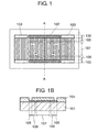
- Fig. 1A is a top view showing a constitution of a surface acoustic wave resonator according to a preferred embodiment 1 of the present invention.
- Fig. 1B is a sectional view of 1B - 1B shown in Fig. 1A .
- Interdigital transducer electrode 102 and reflector electrodes 103 are formed on piezoelectric substrate 101, and SiO 2 thin film 104 is further formed thereon.
- Interdigital transducer electrode 102 includes bus-bar electrode regions 105, dummy electrode regions 106 and finger overlap region 107.
- Interdigital transducer electrode 102 is apodization-weighted in order to control the spurious in the transverse mode.
- Dummy electrode region 106 denotes a region representing a minimum length of a dummy electrode in interdigital transducer electrode 102
- finger overlap region 107 denotes a region representing a crossover maximum length in interdigital transducer electrode 102.
- SiO 2 thin film 104 is removed so that the electrodes are exposed in upper sections of bus-bar electrode regions 105 of interdigital transducer electrode 102, which means that a thickness of SiO 2 thin film 104 is zero therein.
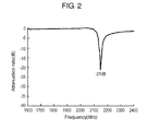
- Fig. 2 shows a frequency versus attenuation rate of the surface acoustic wave resonator thus constituted.
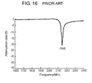
- Fig. 16 shows an attenuation rate of the conventional surface acoustic wave resonator shown in Figs. 15A and 15B for comparison.
- piezoelectric substrate 101 As piezoelectric substrate 101 is used a LiNbO 3 substrate which is a rotor Y-cut having the cut degree of five degrees. A material including Al as its main constituent is used for the electrodes.
- the film thicknesses of the electrode and SiO 2 thin film 104 show values normalized by a wavelength, which are respectively 8% and 20%. As shown in Figs.
- a maximum attenuation in the surface acoustic wave resonator according to the present invention is -21 dB, while the maximum attenuation in the conventional surface acoustic wave resonator is -19 dB.
- the improvement of the characteristics of the surface acoustic wave resonator according to the present invention is thereby confirmed.
- the Q value at an anti-resonance frequency the Q value is 230 in the surface acoustic wave resonator according to the present invention, while the Q value in the conventional surface acoustic wave resonator is 194.
- the improvement of the resonator characteristics is achieved.
- the possible reason for the improvement is that an acoustic velocity of the surface acoustic wave in bus-bar electrode regions 105 is faster than the acoustic velocity in finger overlap region 107 in the surface acoustic wave resonator because SiO 2 thin film 104 in the upper sections of bus-bar electrode regions 105 is removed so that the electrodes are exposed, which controls the leak of the surface acoustic wave in the transverse direction, in other words, in the direction of the bus-bar electrodes, thereby allowing the surface acoustic wave to be more effectively contained.
- the characteristics of the surface acoustic wave resonator can be improved, and the surface acoustic wave resonator which is superior can be thereby realized.
- etching may be adopted after the SiO 2 thin film is formed, or the upper sections of bus-bar electrode regions 105 in interdigital transducer electrode 102 may be masked before the SiO 2 thin film is formed so that the SiO 2 thin film cannot be formed.
- SiO 2 thin film 104 in the upper sections of bus-bar electrode regions 105 in interdigital transducer electrode 102 is removed.
- a constitution shown in Figs. 3A and 3B may be adopted.
- Fig. 3A is a top view of another constitution of the surface acoustic wave resonator according to the preferred embodiment 1.
- Fig. 3B is a sectional view of 3B - B shown in Fig. 3A .
- the constitution is different to that of Fig. 1 in that SiO 2 thin film 104 in the upper sections of dummy electrode regions 106 of interdigital transducer electrode 102 in the surface acoustic wave resonator is removed.
- Fig. 1 SiO 2 thin film 104 in the upper sections of dummy electrode regions 106 of interdigital transducer electrode 102 in the surface acoustic wave resonator is removed.
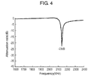
- FIG. 4 shows an attenuation rate of the surface acoustic wave resonator thus constituted.
- the maximum attenuation which is -23 dB
- the Q value at the anti-resonance point is 245, which also shows the improvement.
- the characteristics of the surface acoustic wave resonator can be further improved when SiO 2 thin film 104 of dummy electrode regions 106 is removed.
- SiO 2 thin film 104 in the upper sections of bus-bar electrode regions 105 and dummy electrode regions 106 in interdigital transducer electrode 102 is entirely removed.
- the present preferred embodiment is not limited to the removal in such a manner, and SiO 2 thin film 104 in one of the regions may be removed.
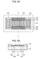
- the surface acoustic wave resonator may be constituted as shown in Fig. 5A.
- Fig. 5A is a top view showing another constitution of the surface acoustic wave resonator according to the preferred embodiment 1
- Fig. 5B is a sectional view of 5B - 5B shown in Fig. 5B .
- the region where SiO 2 thin film 104 is removed may be extended to gap regions between dummy electrode regions 106 and finger overlap region 107 in interdigital transducer electrode 102.
- SiO 2 thin film 104 is preferably left in the upper section of finger overlap region 107 which is a main propagation path of surface acoustic wave because the removal of SiO 2 thin film 104 in the upper section of finger overlap region 107 may lead to the deterioration of the resonator characteristics. Therefore, SiO 2 thin film 104 is preferably removed on dummy electrode region106 side relative to a maximum crossover width.
- SiO 2 thin film 104 is entirely removed from the upper sections of bus-bar electrode regions 105 or dummy electrode regions 106 in interdigital transducer electrode 102, in other words, the thickness of SiO 2 thin film 104 is zero therein.
- the present preferred embodiment is not limited to the removal in such a manner.
- bus-bar electrode regions 105 may be thinner than SiO 2 thin film 104 in the upper section of finger overlap region 107.
- Any constitution capable of increasing the acoustic velocity of the surface acoustic wave in the surface acoustic wave resonator in comparison to the acoustic velocity in finger overlap region 107 by changing the constitutions of the upper section of finger overlap region 107 and the upper sections of bus-bar electrode regions 105 or dummy electrode regions 106 in the surface acoustic wave resonator is adoptable.
- SiO 2 thin film 104 in any of the upper sections of bus-bar electrode regions 105 or dummy electrode regions 106 in interdigital transducer electrode 102a is removed, however, SiO 2 thin film 104 may be removed from a part thereof.
- SiO 2 thin film 104 in a part of bus-bar electrode regions 105 or dummy electrode regions 106 in interdigital transducer electrode 102 is removed, or SiO 2 thin film 104 is very thin, an effect similar to that of the present invention can be obtained.
- the LiNbO 3 substrate which is the rotor Y-cut having the cut degree of five degrees, is used as piezoelectric substrate 101, and the film thicknesses of the electrode and SiO 2 thin film 104 are normalized by the wavelength, which are respectively 8% and 20%.
- the present preferred embodiment is not limited thereto.
- the cut angle of the LiNbO 3 substrate is within the range of approximately -10 to +30 degrees, the surface acoustic wave resonator superior in its broadband and temperature characteristic can be realized in the case where the surface acoustic wave resonator is constituted as described in the present invention.
- the material used for the electrode includes Al as its main constituent in the description, however, the material is not limited thereto. Cu, Au or any other material may be used.
- SiO 2 thin film 104 is used as the dielectric thin film in the description, however, any other dielectric material or a multilayered structure formed therefrom can also be applied.
- reflector electrode 103 is not limited to that of the present preferred embodiment.
- SiO 2 thin film 104 in the upper sections of reflector electrodes 103 in regions corresponding to bus-bar electrode regions 105 and dummy electrode regions 106 in interdigital transducer electrode 102 may be removed or may be thinned. According to the constitution, the reduction of the leak of the surface acoustic wave in the transverse direction can be expected.
- interdigital transducer electrode 102 is apodization-weighted, which, however, may not be limited to the constitution.
- the surface acoustic wave resonator comprises the reflector electrodes.
- the reflector electrodes are not particularly necessary to obtain the expected effect.
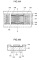
- Fig. 6A is a top view showing a constitution of a surface acoustic wave resonator according to a preferred embodiment 2 of the present invention.
- Fig. 6B is a sectional view of 6B — 6B shown in Fig. 6A .
- Interdigital transducer electrode 702 and reflector electrodes 703 are formed on piezoelectric substrate 701, and SiO 2 thin film 704 is further formed thereon.
- Interdigital transducer electrode 702 includes bus-bar electrode regions 705, dummy electrode regions 706 and finger overlap region 707, wherein the interdigital transducer electrode of the normal type which is not subjected to the apodized-weighting is adopted.
- Dummy electrode region 706 denotes a region representing a minimum length of the dummy electrode in interdigital transducer electrode 702, while finger overlap region 707 denotes region representing a crossover maximum length of the interdigital transducer electrode.
- dummy electrode weighing 708 which is metallized. The metallized region is increased outward from the center, and the length of the dummy electrode is gradually shorter.
- SiO 2 thin film 704 is removed from bus-bar electrode regions 705 and dummy electrodes 706 in interdigital transducer electrode 702 and upper sections thereof.
- Figs. 7A and 7B show an attenuation rate of the surface acoustic wave resonator thus constituted.
- Figs. 7A and 7B show the attenuation rate of the same surface acoustic wave resonator, and a vertical axis shown in Fig. 7A is enlarged in Fig. 7B .
- Figs. 9A and 9B show an attenuation rate of a surface acoustic wave resonator as shown in Fig. 8A and 8B for comparison.
- Fig. 8A is a top view showing a constitution of a surface acoustic wave resonator according to the preferred embodiment 2 for comparison.
- Fig. 8A is a top view showing a constitution of a surface acoustic wave resonator according to the preferred embodiment 2 for comparison.
- FIG. 8B is a sectional view of 8B - 8B shown in Fig. 8A .
- a vertical axis shown in Fig. 9A is enlarged in Fig. 9B .
- the piezoelectric substrate is used the LiNbO 3 substrate which is the rotor Y-cut having the cut degree of five degrees, and the material including Al as its main constituent is used for the electrode.
- the film thicknesses of the electrode and the SiO 2 thin film are normalized by the wavelength, which are respectively 8% and 20%.
- SiO 2 thin film 704 is removed from dummy electrode regions 706 including metallized dummy electrode weighting 708.
- Figs. 9A and 9B show the appearance of spurious 1001 in the transverse mode. In Fig. 7A and 7B , the spurious is controlled, and the superior resonator characteristics are thereby obtained.
- the maximum attenuation in the surface acoustic wave resonator according to the present invention is -20 dB as shown in Fig. 7A
- the maximum attenuation in the surface acoustic wave resonator for comparison is -18 dB as shown in Fig. 9A .
- the improvement of the characteristics of the surface acoustic wave resonator is realized at the same time in the constitution according to the present invention.
- the possible reason for the improvement is that an acoustic velocity of the surface acoustic wave in dummy electrode regions 706 in the surface acoustic wave resonator is faster than the acoustic velocity in finger overlap region 707 because SiO 2 thin film 704 is removed from the upper sections of dummy electrode regions 706, which controls the leak of the surface acoustic wave in the transverse direction, in other words, in the direction of dummy electrode regions 706, thereby allowing the surface acoustic wave to be more effectively contained.
- the SiO 2 thin film is not formed in the upper sections of dummy electrode regions to which metallized dummy electrode weighting 708 is applied in the constitution according to the present invention. Accordingly, the spurious 1001 in the transverse mode can be effectively controlled, and further, the resonator characteristics can be effectively improved.
- the spurious in the transverse mode can be controlled by the interdigital transducer electrode of the normal type which is not subjected to the apodized-weighting, the deterioration of the resonator characteristics due to the Q value resulting from the apodized-weighting can be prevented, which is advantageous in terms of the characteristics in order to realize the surface acoustic wave resonator.
- the resonator size can be reduced in the case of the surface acoustic wave resonator according to the present invention capable of controlling the spurious in the transverse mode without the apodized-weighting in comparison to the conventional surface acoustic wave resonator subjected to the apodized-weighting.
- the surface acoustic wave resonator according to the present invention can be downsized.
- dummy electrode regions 706 in interdigital transducer electrode 702 are weighted, and SiO 2 thin films 704 thereon is removed.
- the characteristics of the surface acoustic wave resonator can be improved, and the surface acoustic wave resonator which is superior can be realized.
- SiO 2 thin film 704 is removed from the upper sections of dummy electrode regions 706 in interdigital transducer electrode 702, however, SiO 2 thin film 704 may be removed from the upper sections of both of dummy electrode regions 706 and bus-bar electrode regions 705.
- SiO 2 thin film 704 is entirely removed in the description, however, the removal may not be necessary.
- SiO 2 thin film 704 in the upper sections of dummy electrode regions 706 may be adapted to be thinner than SiO 2 thin film in the upper section of finger overlap region 707. Any constitution capable of increasing the acoustic velocity of the surface acoustic wave in dummy electrode regions 706 in the surface acoustic wave resonator in comparison to the acoustic velocity in finger overlap region 707 by changing the constitutions of the upper section of finger overlap region 707 and the upper sections of dummy electrode regions 706 in the surface acoustic wave resonator is adoptable.
- SiO 2 thin film 704 in any of the upper sections of dummy electrode regions 706 is removed in the description, however, SiO 2 thin film 704 may be removed from a part thereof In other words, as far as SiO 2 thin film 704 in a part of dummy electrode regions 706 is removed, or SiO 2 thin film 704 therein is thinned, an effect similar to that of the present invention can be obtained.
- SiO 2 thin film 704 in a part of bus-bar electrode regions 705 in interdigital transducer electrode 702 may be removed, or SiO 2 thin film 704 therein may be thinned.
- the length of dummy electrode is gradually shorter because the shape of dummy weighting is metallized outward from the center, however, the present invention is not limited thereto.
- the dummy electrode regions are subjected to some kind of weighting, and SiO 2 thin film 704 is removed or thinned, an effect similar to that of the present invention can be obtained.
- the LiNbO 3 substrate which is the rotor Y-cut having the cut degree of five degrees, is used as the piezoelectric substrate, and the film thicknesses of the electrode and SiO 2 thin film 704 are normalized by the wavelength, which are respectively 8% and 20%, however, the present invention is not limited thereto.
- the cut degree of the LiNbO 3 substrate is within the range of approximately -10 to +30 degrees, the surface acoustic wave resonator superior in its broadband and temperature characteristic can be obtained when the constitution according to the present invention is applied thereto.
- the material for the electrode includes Al as its main constituent, however, the present invention is not limited thereto. Cu, Au or any other material may be used.
- SiO 2 thin film 704 is used as the dielectric thin film in the description, however, any other material or a multilayered structure formed therefrom may be adopted.
- Reflector electrodes 703 are not necessarily constituted as described above. SiO 2 thin film 704 in the upper sections of reflector electrodes 703 in the regions corresponding to bus-bar electrode regions 705 and dummy electrode regions 706 may be removed or thinned. In that case, the reduction of the leak of the surface acoustic wave in the transverse direction in the reflector can be expected.
- interdigital transducer electrode 702 The electrodes of the normal type are used as interdigital transducer electrode 702 in the present preferred embodiment, however, the apodization-weighted interdigital transducer electrode may be combined. In that case, the control of the spurious can be effectively realized.
- the surface acoustic wave resonator comprises the reflector electrodes, however, the present invention, which is applied to the interdigital transducer electrode, can achieve the effect without the reflector electrodes.
- Fig. 11A is a top view illustrating the constitution of the surface acoustic wave resonator
- Fig. 11B is a sectional view of 11B - 11B shown in Fig. 11A
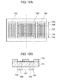
- Fig. 12A is a top view showing a constitution of the surface acoustic wave resonator for comparison
- Fig. 12B is a sectional view of 12B - 12B shown in Fig. 12A .
- Two examples were compared to each other, the examples being respectively: the region where the dielectric thin film is not formed is limited to the upper sections of the dummy and bus-bar regions as shown in Figs.
- the region where the dielectric thin film is not formed includes a part of the finger overlap region as shown in Figs. 12A and 12B .
- the crossover width in the comparison is 25 ⁇ m.
- the region where the dielectric thin film is not formed is provided inward of the finger overlap region by 1 ⁇ m.
- the electrode of the normal type not subjected to the dummy electrode weighting was used in the surface acoustic wave resonator.
- Fig. 13 shows characteristics of the surface acoustic wave resonator shown in Fig. 11A and 11B .
- Fig. 14 shows characteristics of the surface acoustic wave resonator shown in Fig. 12A and 12B .
- the dielectric thin film is preferably formed over the whole finger overlap region.
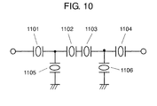
- Fig. 10 shows a constitution of a surface acoustic wave filter according to a preferred embodiment 3 of the present invention.
- 1101, 1102, 1103 and 1104 denote serial-arm surface acoustic wave resonators
- 1105 and 1106 denote parallel-arm surface acoustic wave resonators.
- the surface acoustic wave resonators 1101, 1102, 1103, 1104, 1105 and 1106 the surface acoustic wave resonator shown in the preferred embodiment 1 or 2 is used.
- the surface acoustic wave filter of the ladder type having superior characteristics can be realized.
- the surface acoustic wave filter of the ladder type comprising the six surface acoustic wave resonators 1101, 1102, 1103, 1104, 1105 and 1106 is described, however, the number of the surface acoustic wave resonators to be provided and the constitution of the filter are not limited thereto.
- the surface acoustic wave resonator constituted as described in the preferred embodiment 1 or 2 is applied to at least one of the surface acoustic wave resonators constituting the surface acoustic wave filter, the expected improvements can be obtained.
- interdigital transducer electrode 102 or 702 when the constitution of interdigital transducer electrode 102 or 702 according to the preferred embodiment 1 or 2 is applied, not only to the surface acoustic wave filer of the ladder type comprising the surface acoustic wave resonators provided with reflector electrodes 103 or 703 on the both sides of interdigital transducer electrode 102 or 702, but also to a longitudinal-coupled mode filter provided with a plurality of interdigital transducer electrodes 102 or 702 adjacent to each other, characteristics of the vertical-mode surface acoustic wave filter can also be effectively improved.
- the present invention is not limitedly applied to the surface acoustic wave filter, but is also applicable to an antenna duplexer comprising transmission and reception filter.
- the antenna duplexer can realize superior characteristics.
- the surface acoustic wave resonator according to the present invention can exert such effects that the leak of the surface acoustic wave in the transverse direction is improved and the surface acoustic wave resonator having the superior characteristics is realized. Further, in the case where the surface acoustic wave filter and the antenna duplexer comprises the surface acoustic wave resonator thus constituted, the surface acoustic wave filter and the antenna duplexer can effectively obtain the superior characteristics.
Landscapes
- Physics & Mathematics (AREA)
- Acoustics & Sound (AREA)
- Engineering & Computer Science (AREA)
- Manufacturing & Machinery (AREA)
- Surface Acoustic Wave Elements And Circuit Networks Thereof (AREA)
Applications Claiming Priority (2)
| Application Number | Priority Date | Filing Date | Title |
|---|---|---|---|
| JP2006351247 | 2006-12-27 | ||
| PCT/JP2007/074084 WO2008078573A1 (fr) | 2006-12-27 | 2007-12-14 | Résonateur d'onde acoustique de surface, filtre d'onde acoustique de surface utilisant le résonateur d'onde acoustique de surface, et duplexeur d'antenne |
Publications (2)
| Publication Number | Publication Date |
|---|---|
| EP1962424A1 true EP1962424A1 (fr) | 2008-08-27 |
| EP1962424A4 EP1962424A4 (fr) | 2013-04-03 |
Family
ID=39562367
Family Applications (1)
| Application Number | Title | Priority Date | Filing Date |
|---|---|---|---|
| EP07850596A Withdrawn EP1962424A4 (fr) | 2006-12-27 | 2007-12-14 | Résonateur d'onde acoustique de surface, filtre d'onde acoustique de surface utilisant le résonateur d'onde acoustique de surface, et duplexeur d'antenne |
Country Status (6)
| Country | Link |
|---|---|
| US (1) | US7965155B2 (fr) |
| EP (1) | EP1962424A4 (fr) |
| JP (2) | JP4569699B2 (fr) |
| KR (1) | KR100963341B1 (fr) |
| CN (1) | CN101379699B (fr) |
| WO (1) | WO2008078573A1 (fr) |
Cited By (10)
| Publication number | Priority date | Publication date | Assignee | Title |
|---|---|---|---|---|
| WO2011088904A1 (fr) * | 2010-01-25 | 2011-07-28 | Epcos Ag | Convertisseur électroacoustique doté de pertes réduites par une émission transversale et de performances améliorées par une suppression des modes transversaux |
| US20110215883A1 (en) * | 2010-03-02 | 2011-09-08 | Panasonic Corporation | Acoustic wave resonator and acoustic wave filter using the same |
| WO2012076517A1 (fr) * | 2010-12-07 | 2012-06-14 | Epcos Ag | Convertisseur electro-acoustique a pertes reduites grace a une emission transversale, et de meilleure perfomance due a la suppression de modes transversaux |
| US8222973B2 (en) | 2009-06-04 | 2012-07-17 | Murata Manufacturing Co., Ltd. | Elastic wave resonator, ladder filter and duplexer |
| WO2012132238A1 (fr) * | 2011-03-25 | 2012-10-04 | Panasonic Corporation | Dispositif à ondes acoustiques à modes transversaux d'ordre supérieur réduits |
| US20140001919A1 (en) * | 2011-03-22 | 2014-01-02 | Panasonic Corporation | Elastic wave element |
| US8698578B2 (en) | 2009-05-27 | 2014-04-15 | Panasonic Corporation | Acoustic wave resonator and duplexer using same |
| WO2015007319A1 (fr) | 2013-07-18 | 2015-01-22 | Epcos Ag | Transducteur électroacoustique avec suppression améliorée de modes indésirables |
| RU2602392C1 (ru) * | 2015-11-09 | 2016-11-20 | федеральное государственное автономное образовательное учреждение высшего образования "Южный федеральный университет" | Фильтр на поверхностных акустических волнах |
| KR20210030459A (ko) * | 2018-09-20 | 2021-03-17 | 가부시키가이샤 무라타 세이사쿠쇼 | 탄성파 장치 |
Families Citing this family (35)
| Publication number | Priority date | Publication date | Assignee | Title |
|---|---|---|---|---|
| JP5115184B2 (ja) * | 2007-12-25 | 2013-01-09 | パナソニック株式会社 | 弾性境界波デバイス、及びそれを用いたフィルタ、アンテナ共用器 |
| JP5195443B2 (ja) * | 2009-01-13 | 2013-05-08 | 株式会社村田製作所 | 弾性波装置 |
| CN102204092B (zh) * | 2009-02-25 | 2014-03-12 | 松下电器产业株式会社 | 弹性波元件和弹性波滤波器 |
| US9425766B2 (en) | 2009-11-02 | 2016-08-23 | Skyworks Panasonic Filter Solutions Japan Co., Ltd. | Elastic wave element, and electrical apparatus and duplexer using same |
| CN102652395B (zh) * | 2010-02-22 | 2015-05-20 | 天工松下滤波方案日本有限公司 | 天线共用器 |
| JP5422441B2 (ja) * | 2010-02-26 | 2014-02-19 | 太陽誘電株式会社 | 弾性波デバイス |
| CN101860342B (zh) * | 2010-04-29 | 2013-12-18 | 贵州大学 | 汇流条兼作反射栅型idt结构的saw器件 |
| US9391589B2 (en) * | 2011-01-24 | 2016-07-12 | Epcos Ag | Surface acoustic wave filter on a lithium niobate substrate |
| SG186395A1 (en) | 2011-05-19 | 2013-01-30 | Taiyo Yuden Kk | Acoustic wave device and module |
| WO2014103953A1 (fr) * | 2012-12-26 | 2014-07-03 | 株式会社村田製作所 | Filtre en échelle |
| JP6504551B2 (ja) * | 2013-06-10 | 2019-04-24 | 太陽誘電株式会社 | 共振器、フィルタおよび分波器 |
| JP6335473B2 (ja) * | 2013-11-01 | 2018-05-30 | 太陽誘電株式会社 | 弾性表面波デバイス及びフィルタ |
| JP6355328B2 (ja) * | 2013-12-19 | 2018-07-11 | 太陽誘電株式会社 | 弾性表面波デバイス及びフィルタ |
| WO2015182521A1 (fr) * | 2014-05-26 | 2015-12-03 | 株式会社村田製作所 | Dispositif à ondes élastiques et filtre à échelle |
| DE102014111828A1 (de) * | 2014-08-19 | 2016-02-25 | Epcos Ag | Mit akustischen Oberflächenwellen arbeitender Eintorresonator |
| CN104980117A (zh) * | 2015-06-15 | 2015-10-14 | 电子科技大学 | 一种耐高温的柔性声表面波器件及其制造方法 |
| CN107852143B (zh) * | 2015-07-28 | 2021-02-26 | 株式会社村田制作所 | 弹性波装置 |
| SG11201903365SA (en) * | 2016-10-20 | 2019-05-30 | Skyworks Solutions Inc | Elastic wave device with sub-wavelength thick piezoelectric layer |
| JP6913619B2 (ja) * | 2017-12-12 | 2021-08-04 | 株式会社村田製作所 | マルチプレクサ、高周波フロントエンド回路及び通信装置 |
| KR20190138096A (ko) * | 2018-06-04 | 2019-12-12 | (주)와이솔 | 표면 탄성파 소자 |
| CN109309485A (zh) * | 2018-11-27 | 2019-02-05 | 中电科技德清华莹电子有限公司 | 采用畴反转区的声表面波谐振结构滤波器 |
| CN109327200A (zh) * | 2018-11-27 | 2019-02-12 | 中电科技德清华莹电子有限公司 | 一种声表面波谐振结构滤波器 |
| CN110572138A (zh) * | 2019-10-08 | 2019-12-13 | 开元通信技术(厦门)有限公司 | 一种滤波装置及其制作方法 |
| US11811392B2 (en) | 2019-10-23 | 2023-11-07 | Skyworks Solutions, Inc. | Surface acoustic wave resonator with suppressed transverse modes using selective dielectric removal |
| US11870421B2 (en) | 2019-10-23 | 2024-01-09 | Skyworks Solutions, Inc. | Surface acoustic wave resonator with suppressed transverse modes using second bus bar |
| US12231111B2 (en) * | 2020-04-30 | 2025-02-18 | Rf360 Singapore Pte. Ltd. | Surface acoustic wave electroacoustic device for reduced transversal modes |
| JP2023123880A (ja) * | 2020-05-27 | 2023-09-06 | 株式会社村田製作所 | 弾性波装置 |
| CN113098432B (zh) * | 2021-04-08 | 2025-07-15 | 江苏卓胜微电子股份有限公司 | 一种声表面波谐振器和射频滤波器 |
| US12506464B2 (en) | 2021-12-06 | 2025-12-23 | Skyworks Solutions, Inc. | Multi-band surface acoustic wave filters |
| US12294351B2 (en) | 2021-12-22 | 2025-05-06 | Skyworks Solutions, Inc. | Acoustic wave device with mini bus bars |
| US12587171B2 (en) | 2022-03-18 | 2026-03-24 | Skyworks Solutions, Inc. | Passband filter combining two sets of components |
| US12525494B2 (en) | 2022-03-30 | 2026-01-13 | Skyworks Solutions, Inc. | Composited carrier for microphone package |
| CN115276593B (zh) * | 2022-06-27 | 2023-03-28 | 上海馨欧集成微电有限公司 | 一种声波谐振器及滤波器 |
| WO2024191696A1 (fr) * | 2023-03-15 | 2024-09-19 | Qorvo Us, Inc. | Dispositif à ondes acoustiques en mode trapézoïdal |
| CN119030491B (zh) * | 2024-07-30 | 2025-06-17 | 上海馨欧集成微电有限公司 | 一种声波谐振器、声波滤波器及通信设备 |
Family Cites Families (25)
| Publication number | Priority date | Publication date | Assignee | Title |
|---|---|---|---|---|
| US3760204A (en) * | 1972-03-01 | 1973-09-18 | Motorola Inc | Acoustic surface wave resonator |
| JPS6162221A (ja) * | 1984-09-04 | 1986-03-31 | Nec Corp | 弾性表面波共振子 |
| US4978879A (en) | 1988-07-27 | 1990-12-18 | Fujitsu Limited | Acoustic surface wave element |
| JPH02295211A (ja) * | 1989-05-09 | 1990-12-06 | Fujitsu Ltd | エネルギー閉じ込め型弾性表面波素子 |
| US4999535A (en) * | 1989-09-25 | 1991-03-12 | The United States Of America As Represented By The Secretary Of The Army | Saw transducer with improved bus-bar design |
| JPH03158014A (ja) * | 1989-11-15 | 1991-07-08 | Fujitsu Ltd | 弾性表面波素子 |
| JPH06164297A (ja) | 1992-02-12 | 1994-06-10 | Kokusai Electric Co Ltd | 弾性表面波共振子 |
| JPH05335879A (ja) * | 1992-05-28 | 1993-12-17 | Fujitsu Ltd | 弾性表面波素子 |
| JPH06152299A (ja) * | 1992-11-09 | 1994-05-31 | Fujitsu Ltd | 弾性表面波デバイス |
| JP3201088B2 (ja) * | 1993-08-20 | 2001-08-20 | 株式会社明電舎 | 弾性表面波共振子 |
| JP3226472B2 (ja) * | 1996-05-14 | 2001-11-05 | 富士通株式会社 | 弾性表面波多重モードフィルタ |
| JPH1022765A (ja) * | 1996-07-08 | 1998-01-23 | Hitachi Ltd | 弾性表面波共振子及び共振子型フィルタ |
| JPH10303681A (ja) * | 1997-04-24 | 1998-11-13 | Kyocera Corp | 弾性表面波装置 |
| JPH1174751A (ja) * | 1997-08-28 | 1999-03-16 | Murata Mfg Co Ltd | 弾性表面波装置 |
| JP3317273B2 (ja) * | 1998-08-25 | 2002-08-26 | 株式会社村田製作所 | 表面波共振子、フィルタ、共用器、通信機装置 |
| JP3863712B2 (ja) * | 2000-09-06 | 2006-12-27 | 株式会社日立製作所 | 弾性表面波共振器 |
| JP4109877B2 (ja) | 2001-03-04 | 2008-07-02 | 和彦 山之内 | 弾性表面波機能素子 |
| EP1239588A2 (fr) * | 2001-03-04 | 2002-09-11 | Kazuhiko Yamanouchi | Substrat pour ondes acoustiques de surface et élément fonctionnel à ondes acoustiques de surface |
| JP2003198317A (ja) * | 2001-12-21 | 2003-07-11 | Fujitsu Media Device Kk | 弾性表面波共振子及び弾性表面波フィルタ |
| EP1324489A1 (fr) * | 2001-12-21 | 2003-07-02 | Temex | Procédé de réalisation d'arrangements de filtrage à ondes acoustiques de surface et arrangement de filtrage obtenu selon ce procédé |
| JP4305173B2 (ja) * | 2002-12-25 | 2009-07-29 | パナソニック株式会社 | 電子部品およびこの電子部品を用いた電子機器 |
| US7453334B1 (en) * | 2005-03-21 | 2008-11-18 | Triquint Semiconductor, Inc. | Leaky SAW resonator and method |
| JP2007110342A (ja) * | 2005-10-12 | 2007-04-26 | Kyocera Corp | 弾性表面波素子及びその製造方法 |
| WO2007094368A1 (fr) * | 2006-02-16 | 2007-08-23 | Matsushita Electric Industrial Co., Ltd. | dispositif à onde acoustique de surface, filtre à onde acoustique de surface employant ledit dispositif et duplexeur d'antenne, et appareil électronique employant ledit filtre |
| JP4975377B2 (ja) * | 2006-06-06 | 2012-07-11 | 太陽誘電株式会社 | 弾性境界波素子、共振器およびフィルタ |
-
2007
- 2007-12-14 US US12/094,324 patent/US7965155B2/en active Active
- 2007-12-14 EP EP07850596A patent/EP1962424A4/fr not_active Withdrawn
- 2007-12-14 JP JP2008518531A patent/JP4569699B2/ja active Active
- 2007-12-14 WO PCT/JP2007/074084 patent/WO2008078573A1/fr not_active Ceased
- 2007-12-14 CN CN2007800046075A patent/CN101379699B/zh active Active
- 2007-12-14 KR KR20087012167A patent/KR100963341B1/ko active Active
-
2010
- 2010-08-06 JP JP2010177201A patent/JP5012977B2/ja active Active
Cited By (20)
| Publication number | Priority date | Publication date | Assignee | Title |
|---|---|---|---|---|
| US8698578B2 (en) | 2009-05-27 | 2014-04-15 | Panasonic Corporation | Acoustic wave resonator and duplexer using same |
| US8222973B2 (en) | 2009-06-04 | 2012-07-17 | Murata Manufacturing Co., Ltd. | Elastic wave resonator, ladder filter and duplexer |
| US9257960B2 (en) | 2010-01-25 | 2016-02-09 | Epcos Ag | Electroacoustic transducer having reduced losses due to transverse emission and improved performance due to suppression of transverse modes |
| WO2011088904A1 (fr) * | 2010-01-25 | 2011-07-28 | Epcos Ag | Convertisseur électroacoustique doté de pertes réduites par une émission transversale et de performances améliorées par une suppression des modes transversaux |
| CN102714490A (zh) * | 2010-01-25 | 2012-10-03 | 埃普科斯股份有限公司 | 具有通过横向发射减小的损耗和通过抑制横向模态改善的性能的电声转换器 |
| US9673779B2 (en) | 2010-01-25 | 2017-06-06 | Qualcomm Incorporated | Electroacoustic transducer having reduced losses due to transverse emission and improved performance due to suppression of transverse modes |
| CN102714490B (zh) * | 2010-01-25 | 2016-03-16 | 埃普科斯股份有限公司 | 具有通过横向发射减小的损耗和通过抑制横向模态改善的性能的电声转换器 |
| US8487720B2 (en) * | 2010-03-02 | 2013-07-16 | Panasonic Corporation | Acoustic wave resonator and acoustic wave filter using the same |
| US20110215883A1 (en) * | 2010-03-02 | 2011-09-08 | Panasonic Corporation | Acoustic wave resonator and acoustic wave filter using the same |
| US9391256B2 (en) | 2010-12-07 | 2016-07-12 | Epcos Ag | Electroacoustic transducer with reduced losses due to transverse emission and improved performance due to suppression of transverse modes |
| WO2012076517A1 (fr) * | 2010-12-07 | 2012-06-14 | Epcos Ag | Convertisseur electro-acoustique a pertes reduites grace a une emission transversale, et de meilleure perfomance due a la suppression de modes transversaux |
| US20140001919A1 (en) * | 2011-03-22 | 2014-01-02 | Panasonic Corporation | Elastic wave element |
| US9136458B2 (en) * | 2011-03-22 | 2015-09-15 | Skyworks Panasonic Filter Solutions Japan Co., Ltd. | Elastic wave element |
| US9065424B2 (en) | 2011-03-25 | 2015-06-23 | Skyworks Panasonic Filter Solutions Japan Co., Ltd | Acoustic wave device with reduced higher order transverse modes |
| US9640750B2 (en) | 2011-03-25 | 2017-05-02 | Skyworks Filter Solutions Japan Co., Ltd. | Acoustic wave device with suppressed higher order transverse modes |
| WO2012132238A1 (fr) * | 2011-03-25 | 2012-10-04 | Panasonic Corporation | Dispositif à ondes acoustiques à modes transversaux d'ordre supérieur réduits |
| WO2015007319A1 (fr) | 2013-07-18 | 2015-01-22 | Epcos Ag | Transducteur électroacoustique avec suppression améliorée de modes indésirables |
| US10187034B2 (en) | 2013-07-18 | 2019-01-22 | Snaptrack, Inc. | Electroacoustic transducer with improved suppression of unwanted modes |
| RU2602392C1 (ru) * | 2015-11-09 | 2016-11-20 | федеральное государственное автономное образовательное учреждение высшего образования "Южный федеральный университет" | Фильтр на поверхностных акустических волнах |
| KR20210030459A (ko) * | 2018-09-20 | 2021-03-17 | 가부시키가이샤 무라타 세이사쿠쇼 | 탄성파 장치 |
Also Published As
| Publication number | Publication date |
|---|---|
| JP4569699B2 (ja) | 2010-10-27 |
| KR20080077609A (ko) | 2008-08-25 |
| EP1962424A4 (fr) | 2013-04-03 |
| CN101379699B (zh) | 2012-04-11 |
| WO2008078573A1 (fr) | 2008-07-03 |
| CN101379699A (zh) | 2009-03-04 |
| JPWO2008078573A1 (ja) | 2010-04-22 |
| US20100219905A1 (en) | 2010-09-02 |
| US7965155B2 (en) | 2011-06-21 |
| JP5012977B2 (ja) | 2012-08-29 |
| KR100963341B1 (ko) | 2010-06-14 |
| JP2011019249A (ja) | 2011-01-27 |
Similar Documents
| Publication | Publication Date | Title |
|---|---|---|
| EP1962424A1 (fr) | Résonateur d'onde acoustique de surface, filtre d'onde acoustique de surface utilisant le résonateur d'onde acoustique de surface, et duplexeur d'antenne | |
| US8072293B2 (en) | Surface acoustic wave filter, antenna duplexer and method for manufacturing them | |
| US9035725B2 (en) | Acoustic wave device | |
| USRE39538E1 (en) | Surface acoustic wave arrangement with a junction region between surface acoustic wave structures having a decreasing then increasing finger period | |
| US6873226B2 (en) | Edge-reflection surface acoustic wave filter | |
| US5432392A (en) | Surface wave device | |
| US7425788B2 (en) | Surface acoustic wave device | |
| US7812688B2 (en) | Surface acoustic wave filter, boundary acoustic wave filter, and antenna duplexer using same | |
| US8035460B2 (en) | Surface acoustic wave device, surface acoustic wave filter and antenna duplexer using the same, and electronic equipment using the same | |
| US7728699B2 (en) | Acoustic wave filter | |
| JP7278305B2 (ja) | 弾性波装置、分波器および通信装置 | |
| WO2012132238A1 (fr) | Dispositif à ondes acoustiques à modes transversaux d'ordre supérieur réduits | |
| EP1990915B1 (fr) | Dispositif d'onde acoustique et procede de fabrication correspondant | |
| US10958241B2 (en) | Extractor | |
| WO2010058544A1 (fr) | Filtre accordable | |
| US20070241841A1 (en) | Low-Loss Electro-Acoustic Component | |
| WO2011052218A1 (fr) | Elément à ondes élastiques, duplexeur et appareil électrique utilisant ledit élément | |
| CN116032242B (zh) | 一种具有寄生模态抑制层的声表面波谐振器 | |
| US20060131992A1 (en) | One-port surface acoustic wave resonator and surface acoustic wave filter | |
| JP2982208B2 (ja) | 弾性表面波素子 | |
| US20240171152A1 (en) | Acoustic wave device | |
| JP4544227B2 (ja) | 弾性波共振器およびこれを用いた弾性波フィルタ、アンテナ共用器 | |
| JP2008078981A5 (fr) | ||
| JPH08204501A (ja) | 弾性表面波フィルタ | |
| HK1206157A1 (en) | Antenna sharing device |
Legal Events
| Date | Code | Title | Description |
|---|---|---|---|
| PUAI | Public reference made under article 153(3) epc to a published international application that has entered the european phase |
Free format text: ORIGINAL CODE: 0009012 |
|
| 17P | Request for examination filed |
Effective date: 20080625 |
|
| AK | Designated contracting states |
Kind code of ref document: A1 Designated state(s): AT BE BG CH CY CZ DE DK EE ES FI FR GB GR HU IE IS IT LI LT LU LV MC MT NL PL PT RO SE SI SK TR |
|
| AX | Request for extension of the european patent |
Extension state: AL BA HR MK RS |
|
| RAP1 | Party data changed (applicant data changed or rights of an application transferred) |
Owner name: PANASONIC CORPORATION |
|
| DAX | Request for extension of the european patent (deleted) | ||
| RBV | Designated contracting states (corrected) |
Designated state(s): DE FR GB |
|
| A4 | Supplementary search report drawn up and despatched |
Effective date: 20130305 |
|
| RIC1 | Information provided on ipc code assigned before grant |
Ipc: H03H 9/02 20060101ALI20130227BHEP Ipc: H03H 9/145 20060101AFI20130227BHEP |
|
| 17Q | First examination report despatched |
Effective date: 20130925 |
|
| STAA | Information on the status of an ep patent application or granted ep patent |
Free format text: STATUS: THE APPLICATION IS DEEMED TO BE WITHDRAWN |
|
| 18D | Application deemed to be withdrawn |
Effective date: 20140206 |