EP2071052A2 - Vorrichtung zur Dampfabscheidung eines Kupferfilms - Google Patents
Vorrichtung zur Dampfabscheidung eines Kupferfilms Download PDFInfo
- Publication number
- EP2071052A2 EP2071052A2 EP09004679A EP09004679A EP2071052A2 EP 2071052 A2 EP2071052 A2 EP 2071052A2 EP 09004679 A EP09004679 A EP 09004679A EP 09004679 A EP09004679 A EP 09004679A EP 2071052 A2 EP2071052 A2 EP 2071052A2
- Authority
- EP
- European Patent Office
- Prior art keywords
- gas
- reactor vessel
- copper
- substrate
- temperature
- Prior art date
- Legal status (The legal status is an assumption and is not a legal conclusion. Google has not performed a legal analysis and makes no representation as to the accuracy of the status listed.)
- Withdrawn
Links
Images
Classifications
-
- C—CHEMISTRY; METALLURGY
- C23—COATING METALLIC MATERIAL; COATING MATERIAL WITH METALLIC MATERIAL; CHEMICAL SURFACE TREATMENT; DIFFUSION TREATMENT OF METALLIC MATERIAL; COATING BY VACUUM EVAPORATION, BY SPUTTERING, BY ION IMPLANTATION OR BY CHEMICAL VAPOUR DEPOSITION, IN GENERAL; INHIBITING CORROSION OF METALLIC MATERIAL OR INCRUSTATION IN GENERAL
- C23C—COATING METALLIC MATERIAL; COATING MATERIAL WITH METALLIC MATERIAL; SURFACE TREATMENT OF METALLIC MATERIAL BY DIFFUSION INTO THE SURFACE, BY CHEMICAL CONVERSION OR SUBSTITUTION; COATING BY VACUUM EVAPORATION, BY SPUTTERING, BY ION IMPLANTATION OR BY CHEMICAL VAPOUR DEPOSITION, IN GENERAL
- C23C14/00—Coating by vacuum evaporation, by sputtering or by ion implantation of the coating forming material
- C23C14/22—Coating by vacuum evaporation, by sputtering or by ion implantation of the coating forming material characterised by the process of coating
-
- C—CHEMISTRY; METALLURGY
- C23—COATING METALLIC MATERIAL; COATING MATERIAL WITH METALLIC MATERIAL; CHEMICAL SURFACE TREATMENT; DIFFUSION TREATMENT OF METALLIC MATERIAL; COATING BY VACUUM EVAPORATION, BY SPUTTERING, BY ION IMPLANTATION OR BY CHEMICAL VAPOUR DEPOSITION, IN GENERAL; INHIBITING CORROSION OF METALLIC MATERIAL OR INCRUSTATION IN GENERAL
- C23C—COATING METALLIC MATERIAL; COATING MATERIAL WITH METALLIC MATERIAL; SURFACE TREATMENT OF METALLIC MATERIAL BY DIFFUSION INTO THE SURFACE, BY CHEMICAL CONVERSION OR SUBSTITUTION; COATING BY VACUUM EVAPORATION, BY SPUTTERING, BY ION IMPLANTATION OR BY CHEMICAL VAPOUR DEPOSITION, IN GENERAL
- C23C16/00—Chemical coating by decomposition of gaseous compounds, without leaving reaction products of surface material in the coating, i.e. chemical vapour deposition [CVD] processes
- C23C16/44—Chemical coating by decomposition of gaseous compounds, without leaving reaction products of surface material in the coating, i.e. chemical vapour deposition [CVD] processes characterised by the method of coating
- C23C16/448—Chemical coating by decomposition of gaseous compounds, without leaving reaction products of surface material in the coating, i.e. chemical vapour deposition [CVD] processes characterised by the method of coating characterised by the method used for generating reactive gas streams, e.g. by evaporation or sublimation of precursor materials
- C23C16/4488—Chemical coating by decomposition of gaseous compounds, without leaving reaction products of surface material in the coating, i.e. chemical vapour deposition [CVD] processes characterised by the method of coating characterised by the method used for generating reactive gas streams, e.g. by evaporation or sublimation of precursor materials by in situ generation of reactive gas by chemical or electrochemical reaction
-
- C—CHEMISTRY; METALLURGY
- C23—COATING METALLIC MATERIAL; COATING MATERIAL WITH METALLIC MATERIAL; CHEMICAL SURFACE TREATMENT; DIFFUSION TREATMENT OF METALLIC MATERIAL; COATING BY VACUUM EVAPORATION, BY SPUTTERING, BY ION IMPLANTATION OR BY CHEMICAL VAPOUR DEPOSITION, IN GENERAL; INHIBITING CORROSION OF METALLIC MATERIAL OR INCRUSTATION IN GENERAL
- C23C—COATING METALLIC MATERIAL; COATING MATERIAL WITH METALLIC MATERIAL; SURFACE TREATMENT OF METALLIC MATERIAL BY DIFFUSION INTO THE SURFACE, BY CHEMICAL CONVERSION OR SUBSTITUTION; COATING BY VACUUM EVAPORATION, BY SPUTTERING, BY ION IMPLANTATION OR BY CHEMICAL VAPOUR DEPOSITION, IN GENERAL
- C23C16/00—Chemical coating by decomposition of gaseous compounds, without leaving reaction products of surface material in the coating, i.e. chemical vapour deposition [CVD] processes
- C23C16/06—Chemical coating by decomposition of gaseous compounds, without leaving reaction products of surface material in the coating, i.e. chemical vapour deposition [CVD] processes characterised by the deposition of metallic material
- C23C16/08—Chemical coating by decomposition of gaseous compounds, without leaving reaction products of surface material in the coating, i.e. chemical vapour deposition [CVD] processes characterised by the deposition of metallic material from metal halides
- C23C16/14—Deposition of only one other metal element
-
- C—CHEMISTRY; METALLURGY
- C23—COATING METALLIC MATERIAL; COATING MATERIAL WITH METALLIC MATERIAL; CHEMICAL SURFACE TREATMENT; DIFFUSION TREATMENT OF METALLIC MATERIAL; COATING BY VACUUM EVAPORATION, BY SPUTTERING, BY ION IMPLANTATION OR BY CHEMICAL VAPOUR DEPOSITION, IN GENERAL; INHIBITING CORROSION OF METALLIC MATERIAL OR INCRUSTATION IN GENERAL
- C23C—COATING METALLIC MATERIAL; COATING MATERIAL WITH METALLIC MATERIAL; SURFACE TREATMENT OF METALLIC MATERIAL BY DIFFUSION INTO THE SURFACE, BY CHEMICAL CONVERSION OR SUBSTITUTION; COATING BY VACUUM EVAPORATION, BY SPUTTERING, BY ION IMPLANTATION OR BY CHEMICAL VAPOUR DEPOSITION, IN GENERAL
- C23C16/00—Chemical coating by decomposition of gaseous compounds, without leaving reaction products of surface material in the coating, i.e. chemical vapour deposition [CVD] processes
- C23C16/44—Chemical coating by decomposition of gaseous compounds, without leaving reaction products of surface material in the coating, i.e. chemical vapour deposition [CVD] processes characterised by the method of coating
- C23C16/448—Chemical coating by decomposition of gaseous compounds, without leaving reaction products of surface material in the coating, i.e. chemical vapour deposition [CVD] processes characterised by the method of coating characterised by the method used for generating reactive gas streams, e.g. by evaporation or sublimation of precursor materials
Definitions
- the present invention relates to a copper film vapor phase deposition method and vapor phase deposition apparatus applied to, e.g., the formation of a wiring material film of a semiconductor device.
- a thin copper (Cu) film used as a wiring material and the like is formed by physical film formation methods such as vacuum deposition, ion plating, and sputtering, and by chemical vapor deposition (CVD).
- CVD chemical vapor deposition
- CVD is generally extensively used because the method has superior surface covering properties.
- a conventionally known copper film formation method using CVD uses a liquid organic copper complex such as copper ⁇ hexafluoroacetylacetonate ⁇ trimethylvinylsilane as a material.
- Jpn. Pat. Appln. KOKAI Publication Nos. 4-72066 , 4-74866 , and 9-53177 disclose methods using organic metal complexes not containing fluorine as materials. These materials are sublimated, transported, and excited by heat, light, or plasma to form a copper film on the surface of a substrate to be processed.
- a copper film vapor phase deposition method comprises the steps of exposing high-purity copper to a plasma of a gas containing chlorine gas to etch the high-purity copper, thereby generating active Cu x Cl y , wherein x is 1 to 3, y is 1 to 3, gas, and forming a copper film by transporting the Cu x Cl y gas onto the surface of a substrate to be processed.
- Another copper film vapor phase deposition method comprises the steps of exposing high-purity copper to a plasma of a gas containing hydrogen chloride gas to etch the high-purity copper, thereby generating active Cu x Cl y , wherein x is 1 to 3, y is 1 to 3, gas, and forming a copper film by transporting the Cu x Cl y gas onto the surface of a substrate to be processed.
- Still another copper film vapor phase deposition method comprises the steps of exposing high-purity copper to a plasma of chlorine gas and hydrogen to etch the high-purity copper, thereby generating a gas mixture containing active Cu x Cl y , wherein x is 1 to 3, y is 1 to 3, gas and hydrogen, and forming a copper film by transporting the gas mixture onto the surface of a substrate to be processed.
- the high-purity copper is preferably heated to 200 to 400°C, and the substrate is preferably heated to 100 to 200°C.
- a copper film vapor phase deposition apparatus comprises a reactor vessel in which a substrate to be processed is placed, high-purity copper set in the reactor vessel to oppose the substrate, a gas supply pipe inserted into the reactor vessel to supply a gas containing chlorine gas or hydrogen chloride gas to the vicinity of the high-purity copper, plasma generating means for generating a plasma of chlorine or hydrogen chloride in the vicinity of the high-purity copper in the reactor vessel, and exhausting means for exhausting a gas in the reactor vessel.
- Another copper film vapor phase deposition apparatus comprises a reactor vessel in which a substrate to be processed is placed, high-purity copper set in the reactor vessel to oppose the substrate, a first gas supply pipe inserted into the reactor vessel to supply a gas containing chlorine to the vicinity of the high-purity copper, a second gas supply pipe inserted into the reactor vessel to supply hydrogen to the vicinity of the high-purity copper, plasma generating means for generating a plasma of chlorine and hydrogen in the vicinity of the high-purity copper in the reactor vessel, and exhausting means for exhausting a gas in the reactor vessel.
- Each copper film vapor phase deposition apparatus preferably further comprises first temperature control means for controlling the temperature of the high-purity copper.
- Each copper film vapor phase deposition apparatus preferably further comprises second temperature control means for controlling the temperature of the substrate.
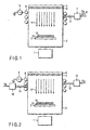
- FIG. 1 is a schematic view showing a copper film vapor phase deposition apparatus according to the first embodiment.
- a second temperature control means e.g., a plate-like heating member 3 on which a substrate to be processed is placed is set.
- High-purity copper e.g., high-purity copper plate 4 is set in the upper portion of the reactor vessel 2 so as to oppose the heating member 3.
- High-purity copper herein mentioned means that the purity of copper is 99.9% or more.
- this high-purity copper need not be a plate but can be, e.g., a block.
- a first temperature control means e.g., a heating/cooling member 5 is placed on the surface of the high-purity copper plate 4 away from the surface opposite to the heating member 3.
- a gas supply pipe 6 for supplying a gas containing chlorine gas (or a gas containing hydrogen chloride gas) is connected to an upper side wall of the reactor vessel 2.
- a flow rate controller 7 is inserted into that portion of the gas supply pipe 6, which is positioned outside the reactor vessel 2.
- An RF coil 8 is wound around the upper side walls of the reactor vessel 2.
- An RF power supply 9 is connected to the RF coil 8 and applies an RF power of 13.56 MHz to this RF coil 8.
- This plasma generating means need not be an inductive coupling type plasma generator but can be a capacitive coupling type plasma generator.
- the high-purity copper plate 4 is set in the upper portion of the reactor vessel 2, and the heating member 3 on which a substrate 10 is to be placed and the exhaust member 1 are set in the lower portion of the reactor vessel 2.
- this vertical positional relationship can also be reversed.
- a copper film formation method using the copper film vapor phase deposition apparatus shown in FIG. 1 will be explained below.
- the substrate 10 is placed on the heating member 3 in the reactor vessel 2.
- the exhaust member 1 is operated to exhaust a gas (air) in the reactor vessel 2 to set a predetermined vacuum degree.
- a gas containing chlorine (Cl 2 ) is supplied into the reactor vessel 2 through the gas supply pipe 6.
- the flow rate of this chlorine-containing gas is controlled by the flow rate controller 7 inserted into the gas supply pipe 6.
- the temperature of the high-purity copper plate 4 placed in the upper portion of the reactor vessel 2 is controlled by the heating/cooling member 5.
- the RF power supply 9 applies an RF power of 13.56 MHz to the RF coil 8, thereby generating chlorine plasma below and near the high-purity copper plate 4 in the reactor vessel 2. If the temperature of the high-purity copper plate 4 excessively rises along with the generation of this chlorine plasma, the heating/cooling member 5 controls the high-purity copper plate 4 to a target temperature.
- This Cu x Cl y flux 11 is transported to the substrate 10 heated by the heating member 3 and precipitates a copper film 12 on the surface of the substrate 10.
- x and y of the Cu x Cl y gas change in accordance with the temperature. For example, this reaction is represented by 2Cu + Cl 2 ⁇ CuCl ⁇ ⁇ 2Cu ⁇ + Cl 2 ⁇
- the copper film has a thickness of 1 nm to 1 ⁇ m.
- the gas containing chlorine (Cl 2 ) it is possible to use, e.g., chlorine gas or a dilute gas which is formed by diluting chlorine gas with an inert gas such as helium or argon and which has a chlorine concentration of 50% or less.
- chlorine gas or a dilute gas which is formed by diluting chlorine gas with an inert gas such as helium or argon and which has a chlorine concentration of 50% or less.
- Heating of the substrate 10 by the heating member 3 is preferably done at a temperature lower than the set temperature of the high-purity copper (e.g., high-purity copper plate) in order to obtain a practical copper film formation rate, thereby promoting adsorption of the Cu x Cl y gas to the substrate surface.
- the temperature of the high-purity copper is set at 200 to 400°C
- the temperature of the substrate is preferably set at, e.g., 100 to 200°C.
- the temperature of the high-purity copper plate 4 By adjusting the temperature of the high-purity copper plate 4 within the range of 0 to 600°C by the heating/cooling member 5, it is possible to control the surface etching rate and etching form in the chlorine plasma atmosphere.
- the lower-limit temperature is one at which chlorine gas does not cohere
- the upper-limit temperature is one at which high-purity copper does not dissolve. That is, when the temperature is raised within the above temperature range, it is possible to increase the etching rate (Cu x Cl y generation amount) and increase the copper film formation speed.
- the temperature is favorably controlled within the range of 200 to 400°C in order to prevent an abrupt etching reaction.
- the pressure of the chlorine gas in the reactor vessel 2 is preferably controlled within the range of 0.1 to 10 Torr, in order to etch the high-purity copper plate at a practical rate in a vacuum atmosphere.
- a gas containing inexpensive chlorine is supplied through the gas supply pipe 6 into the reactor vessel 2 in which the inexpensive high-purity copper (e.g., high-purity copper plate) 4 is placed.
- the RF power supply 9 and the RF coil 8 generate chlorine plasma below and near the high-purity copper plate 4 in the reactor vessel 2.
- the high-purity copper plate 4 is etched by the excited chlorine and reacted to generate Cu x Cl y gas.
- This Cu x Cl y flux 11 is transported to the substrate 10 to form the copper film 12 on the substrate 10.
- this first embodiment it is possible to independently adjust the temperature of high-purity copper, the pressure and flow rate of chlorine gas, and the temperature of a substrate to be processed. This can increase the degree of freedom of control parameters compared to film formation using the conventional sublimation method. As a consequence, a copper film containing no residual impurity such as carbon and having high film quality can be formed on a substrate with high reproducibility.
- a copper film formation method according to the second embodiment will be explained below by using the copper film vapor phase deposition apparatus shown in FIG. 1 described above.
- a substrate 10 to be processed is placed on a heating member 3 in a reactor vessel 2.
- An exhaust member 1 is operated to exhaust a gas (air) in the reactor vessel 2 to set a predetermined vacuum degree.
- a gas containing hydrogen chloride (HCl) is supplied into the reactor vessel 2 through a gas supply pipe 6.
- the flow rate of this hydrogen chloride-containing gas is controlled by a flow rate controller 7 inserted into the gas supply pipe 6.
- the temperature of high-purity copper (e.g., high-purity copper plate) 4 placed in the upper portion of the reactor vessel 2 is controlled by a heating/cooling member 5.
- an RF power supply 9 applies an RF power of 13.56 MHz to an RF coil 8, thereby generating hydrogen chloride plasma below and near the high-purity copper plate 4 in the reactor vessel 2. If the temperature of the high-purity copper plate 4 excessively rises along with the generation of this hydrogen chloride plasma, the heating/cooling member 5 controls the high-purity copper plate 4 to a target temperature.
- This Cu x Cl y flux 11 is transported to the substrate 10 heated by the heating member 3 and precipitates a copper film 12 on the surface of the substrate 10.
- x and y of the Cu x Cl y gas change in accordance with the temperature.
- this reaction is represented by 2Cu + 2HCl ⁇ 2CuCl ⁇ + H2 ⁇ 2Cu ⁇ + Cl 2 ⁇ + H 2
- the copper film has a thickness of 1 nm to 1 ⁇ m.
- the gas containing hydrogen chloride (HCl) it is possible to use, e.g., hydrogen chloride gas or a dilute gas which is formed by diluting hydrogen chloride gas with an inert gas such as helium or argon and which has a chlorine concentration of 50% or less.
- hydrogen chloride gas or a dilute gas which is formed by diluting hydrogen chloride gas with an inert gas such as helium or argon and which has a chlorine concentration of 50% or less.
- Heating of the substrate 10 by the heating member 3 is preferably done at a temperature lower than the set temperature of the high-purity copper (e.g., high-purity copper plate) in order to obtain a practical copper film formation rate, thereby promoting adsorption of the Cu x Cl y gas to the substrate surface.
- the temperature of the high-purity copper is set at 200 to 400°C
- the temperature of the substrate is preferably set at, e.g., 100 to 200°C.
- the temperature of the high-purity copper plate 4 By adjusting the temperature of the high-purity copper plate 4 within the range of 0 to 600°C by the heating/cooling member 5, it is possible to control the surface etching rate and etching form in the hydrogen chloride plasma atmosphere.
- the lower-limit temperature is one at which chlorine gas does not cohere
- the upper-limit temperature is one at which high-purity copper does not dissolve. That is, when the temperature is raised within the above temperature range, it is possible to increase the etching rate (Cu x Cl y generation amount) and increase the copper film formation speed.
- the temperature is favorably controlled within the range of 200 to 400°C in order to prevent an abrupt increase of the etching reaction.
- the pressure of the hydrogen chloride gas in the reactor vessel 2 is preferably controlled within the range of 0.1 to 10 Torr, in order to etch the high-purity copper plate at a practical rate in a vacuum atmosphere.
- a gas containing inexpensive hydrogen chloride is supplied through the gas supply pipe 6 into the reactor vessel 2 in which the inexpensive high-purity copper (e.g., high-purity copper plate) 4 is placed.
- the RF power supply 9 and the RF coil 8 generate hydrogen chloride plasma below and near the high-purity copper plate 4 in the reactor vessel 2.
- the high-purity copper plate 4 is etched by the excited hydrogen chloride and reacted to generate Cu x Cl y gas.
- This Cu x Cl y flux 11 is transported to the substrate 10 to form the copper film 12 on the substrate 10.
- this second embodiment it is possible to independently adjust the temperature of high-purity copper, the pressure and flow rate of hydrogen chloride gas, and the temperature of a substrate to be processed. This can increase the degree of freedom of control parameters compared to film formation using the conventional sublimation method. As a consequence, a copper film containing no impurity such as carbon and having high film quality can be formed on a substrate with high reproducibility.
- FIG. 2 is a schematic view showing a copper film vapor phase deposition apparatus according to the third embodiment.
- the same reference numerals as in FIG. 1 denote the same parts in FIG. 2 , and a detailed description thereof will be omitted.
- This vapor phase deposition apparatus includes a first gas supply pipe 13 connected to an upper side wall of a reactor vessel 2 to supply a gas containing chlorine, and a second gas supply pipe 14 connected to that upper side wall of the reactor vessel 2, which is opposite to the first gas supply pipe 13, to supply hydrogen.
- Flow rate controllers 15 and 16 are inserted into these first and second gas supply pipes 13 and 14, respectively.
- high-purity copper e.g., high-purity copper plate
- a heating member 3 on which a substrate 10 to be processed is placed and an exhaust member 1 are set in the lower portion of the reactor vessel 2.
- this vertical positional relationship can also be reversed.
- the shape of the high-purity copper need not be a plate but can be, e.g., a block.
- a copper film formation method using the copper film vapor phase deposition apparatus shown in FIG. 2 will be explained below.
- the substrate 10 is placed on the heating member 3 in the reactor vessel 2.
- the exhaust member 1 is operated to exhaust a gas (air) in the reactor vessel 2 to set a predetermined vacuum degree.
- a gas containing chlorine (Cl 2 ) is supplied into the reactor vessel 2 through the first gas supply pipe 13, and hydrogen is supplied into the reactor vessel 2 through the second gas supply pipe 14.
- the flow rates of these chlorine-containing gas and hydrogen are controlled by the flow rate controllers 15 and 16 inserted into the gas supply pipes 13 and 14, respectively.
- the temperature of the high-purity copper plate 4 placed in, e.g., the upper portion of the reactor vessel 2 is controlled by a heating/cooling member 5.
- an RF power supply 9 applies an RF power of 13.56 MHz to an RF coil 8, thereby generating a plasma of chlorine + hydrogen below and near the high-purity copper plate 4 in the reactor vessel 2. If the temperature of the high-purity copper plate 4 excessively rises along with the generation of this plasma of chlorine + hydrogen, the heating/cooling member 5 controls the high-purity copper plate 4 to a target temperature.
- This flux 17 is transported to the substrate 10 heated by the heating member 3 and precipitates a copper film 12 on the surface of the substrate 10.
- x and y of the Cu x Cl y gas change in accordance with the temperature.
- this reaction is represented by 2Cu + Cl 2 + H 2 ⁇ 2CuCl ⁇ + H 2 ⁇ 2Cu ⁇ + 2HCl ⁇
- the copper film has a thickness of 1 nm to 1 ⁇ m.
- the gas containing chlorine (Cl 2 ) it is possible to use, e.g., chlorine gas or a dilute gas which is formed by diluting chlorine gas with an inert gas such as helium or argon and which has a chlorine concentration of 50% or less.
- chlorine gas or a dilute gas which is formed by diluting chlorine gas with an inert gas such as helium or argon and which has a chlorine concentration of 50% or less.
- Heating of the substrate 10 by the heating member 3 is preferably done at a temperature lower than the set temperature of the high-purity copper (e.g., high-purity copper plate) in order to obtain a practical copper film formation rate, thereby promoting adsorption of the Cu x Cl y gas to the substrate surface.
- the temperature of the high-purity copper is set at 200 to 400°C
- the temperature of the substrate is preferably set at, e.g., 100 to 200°C.
- the temperature of the high-purity copper plate 4 By adjusting the temperature of the high-purity copper plate 4 within the range of 0 to 600°C by the heating/cooling member 5, it is possible to control the surface etching rate and etching form in the chlorine + hydrogen plasma atmosphere.
- the lower-limit temperature is one at which chlorine gas does not cohere
- the upper-limit temperature is one at which high-purity copper does not dissolve. That is, when the temperature is raised within the above temperature range, it is possible to increase the etching rate (Cu x Cl y generation amount) and increase the copper film formation speed.
- the temperature is favorably controlled within the range of 200 to 400°C in order to prevent an abrupt increase of the etching reaction.
- the pressure of the chlorine gas in the reactor vessel 2 is preferably controlled within the range of 0.1 to 10 Torr, in order to etch the high-purity copper plate at a practical rate in a vacuum atmosphere.
- the pressure of the hydrogen gas in the reactor vessel 2 is preferably controlled within the range of 1 to 10 Torr, in order to efficiently precipitate (form) a copper film by reduction.
- a gas containing inexpensive chlorine and hydrogen are supplied through the first and second gas supply pipes 13 and 14 into the reactor vessel 2 in which the inexpensive high-purity copper (e.g., high-purity copper plate) 4 is placed.
- the RF power supply 9 and the RF coil 8 generate a plasma of chlorine and hydrogen below and near the high-purity copper plate 4 in the reactor vessel 2.
- Etching of the high-purity copper plate 4 by the excited chlorine and dissociation of hydrogen generate the flux 17 of Cu x Cl y and H. This flux 17 is transported to the substrate 10 to form the copper film 12 on the substrate 10.
- this third embodiment it is possible to independently adjust the temperature of high-purity copper, the pressures and flow rates of chlorine gas and hydrogen, and the temperature of a substrate to be processed. This can increase the degree of freedom of control parameters compared to film formation using the conventional sublimation method. As a consequence, a copper film containing no residual impurity such as carbon and having high film quality can be formed on a substrate with high reproducibility.
- a substrate 10 to be processed having a diameter of 300 mm was placed on a heating member 3 in a reactor vessel 2 and heated to 200°C.
- An exhaust member 1 was operated to exhaust a gas (air) in the reactor vessel 2 to set a predetermined vacuum degree.
- chlorine (Cl 2 ) was supplied at a flow rate of 100 sccm into the reactor vessel 2 through a gas supply pipe 6 and a flow rate controller 7.
- the pressure of the chlorine in the reactor vessel 2 was 5 Torr.
- the temperature of high-purity copper plate 4 set in the upper portion of the reactor vessel 2 was controlled to 300°C by a heating/cooling member 5. After the temperature of this high-purity copper plate 4 was thus controlled, an RF power of 13.56 MHz was applied from an RF power supply 9 to an RF coil 8, thereby generating chlorine plasma below and near the high-purity copper plate 4 in the reactor vessel 2.
- the high-purity copper plate 4 was etched by the excited chlorine and reacted to form Cu x Cl y flux 11, thereby precipitating a copper film 12 having a thickness of 500 nm on the surface of the substrate 10. Gases and etching products which did not participate in the reaction were exhausted by the exhaust member 1.
- Example 1 a copper film was uniformly formed on the substrate at a rate of 100 nm/min and a variation of 3% or less. This copper film had characteristics equivalent to the resistivity of bulk copper.
- a substrate 10 to be processed having a diameter of 300 mm was placed on a heating member 3 in a reactor vessel 2 and heated to 170°C.
- An exhaust member 1 was operated to exhaust a gas (air) in the reactor vessel 2 to set a predetermined vacuum degree.
- hydrogen chloride (HCl) was supplied at a flow rate of 100 sccm into the reactor vessel 2 through a gas supply pipe 6 and a flow rate controller 7.
- the pressure of the chlorine in the reactor vessel 2 was 5 Torr.
- the temperature of high-purity copper plate 4 set in the upper portion of the reactor vessel 2 was controlled to 300°C by a heating/cooling member 5. After the temperature of this high-purity copper plate 4 was thus controlled, an RF power of 13.56 MHz was applied from an RF power supply 9 to an RF coil 8, thereby generating hydrogen chloride plasma below and near the high-purity copper plate 4 in the reactor vessel 2.
- the high-purity copper plate 4 was etched by the excited hydrogen chloride and reacted to form Cu x Cl y flux 11, thereby precipitating a copper film 12 having a thickness of 500 nm on the surface of the substrate 10. Gases and etching products which did not participate in the reaction were exhausted by the exhaust member 1.
- Example 2 a copper film was uniformly formed on the substrate at a rate of 100 nm/min and a variation of 3% or less. This copper film had characteristics equivalent to the resistivity of bulk copper.
- a substrate 10 to be processed having a diameter of 300 mm was placed on a heating member 3 in a reactor vessel 2 and heated to 150°C.
- An exhaust member 1 was operated to exhaust a gas (air) in the reactor vessel 2 to set a predetermined vacuum degree.
- chlorine gas was supplied at a flow rate of 100 sccm into the reactor vessel 2 through a first gas supply pipe 13 and a flow rate controller 15.
- hydrogen was supplied at a flow rate of 500 sccm into the reactor vessel 2 through a second gas supply pipe 14 and a flow rate controller 16.
- the pressures of the chlorine gas and hydrogen in the reactor vessel 2 were 2.5 and 5 Torr, respectively.
- the temperature of high-purity copper plate 4 set in the upper portion of the reactor vessel 2 was controlled to 300°C by a heating/cooling member 5.
- Example 3 a copper film was uniformly formed on the substrate at a rate of 100 nm/min and a variation of 3% or less. This copper film had characteristics equivalent to the resistivity of bulk copper.
- the present invention can provide a copper film vapor phase deposition method which can form, with high reproducibility, a copper film containing no residual impurity such as carbon and having high film quality, by using inexpensive high-purity copper and inexpensive chlorine, hydrogen chloride, or chlorine and hydrogen as source gases, and which is useful in, e.g., the formation of wiring material films of a semiconductor device and a liquid crystal display.
- the present invention can provide a copper film vapor phase deposition apparatus capable of forming a copper film having the aforementioned characteristics.
Landscapes
- Chemical & Material Sciences (AREA)
- General Chemical & Material Sciences (AREA)
- Chemical Kinetics & Catalysis (AREA)
- Engineering & Computer Science (AREA)
- Materials Engineering (AREA)
- Mechanical Engineering (AREA)
- Metallurgy (AREA)
- Organic Chemistry (AREA)
- Electrochemistry (AREA)
- Electrodes Of Semiconductors (AREA)
- Drying Of Semiconductors (AREA)
- Chemical Vapour Deposition (AREA)
- Physical Vapour Deposition (AREA)
Applications Claiming Priority (3)
| Application Number | Priority Date | Filing Date | Title |
|---|---|---|---|
| JP2001241168 | 2001-08-08 | ||
| JP2002025975A JP3680029B2 (ja) | 2001-08-08 | 2002-02-01 | 金属薄膜の気相成長方法およびその気相成長装置 |
| EP02013994A EP1284305B1 (de) | 2001-08-08 | 2002-06-26 | Verfahren zur Dampfabscheidung eines Kupferfilms. |
Related Parent Applications (1)
| Application Number | Title | Priority Date | Filing Date |
|---|---|---|---|
| EP02013994A Division EP1284305B1 (de) | 2001-08-08 | 2002-06-26 | Verfahren zur Dampfabscheidung eines Kupferfilms. |
Publications (2)
| Publication Number | Publication Date |
|---|---|
| EP2071052A2 true EP2071052A2 (de) | 2009-06-17 |
| EP2071052A3 EP2071052A3 (de) | 2009-09-16 |
Family
ID=26620215
Family Applications (2)
| Application Number | Title | Priority Date | Filing Date |
|---|---|---|---|
| EP09004679A Withdrawn EP2071052A3 (de) | 2001-08-08 | 2002-06-26 | Vorrichtung zur Dampfabscheidung eines Kupferfilms |
| EP02013994A Expired - Lifetime EP1284305B1 (de) | 2001-08-08 | 2002-06-26 | Verfahren zur Dampfabscheidung eines Kupferfilms. |
Family Applications After (1)
| Application Number | Title | Priority Date | Filing Date |
|---|---|---|---|
| EP02013994A Expired - Lifetime EP1284305B1 (de) | 2001-08-08 | 2002-06-26 | Verfahren zur Dampfabscheidung eines Kupferfilms. |
Country Status (6)
| Country | Link |
|---|---|
| US (3) | US7048973B2 (de) |
| EP (2) | EP2071052A3 (de) |
| JP (1) | JP3680029B2 (de) |
| KR (1) | KR100510039B1 (de) |
| DE (1) | DE60234001D1 (de) |
| TW (1) | TW550677B (de) |
Families Citing this family (56)
| Publication number | Priority date | Publication date | Assignee | Title |
|---|---|---|---|---|
| US20030145790A1 (en) * | 2002-02-05 | 2003-08-07 | Hitoshi Sakamoto | Metal film production apparatus and metal film production method |
| DE60329292D1 (de) | 2002-03-08 | 2009-10-29 | Canon Anelva Corp | Verfahren und Vorrichtung zum Herstellen von Metall-Schichten |
| JP4845455B2 (ja) * | 2005-09-01 | 2011-12-28 | キヤノンアネルバ株式会社 | 薄膜作製装置及び薄膜作製方法 |
| JP4401338B2 (ja) * | 2005-09-06 | 2010-01-20 | キヤノンアネルバ株式会社 | 薄膜作製装置及び薄膜作製方法 |
| JP4401340B2 (ja) * | 2005-09-14 | 2010-01-20 | キヤノンアネルバ株式会社 | 薄膜作製装置及び薄膜作製方法 |
| KR100960958B1 (ko) * | 2007-12-24 | 2010-06-03 | 주식회사 케이씨텍 | 박막 증착 장치 및 증착 방법 |
| US10181653B2 (en) | 2016-07-21 | 2019-01-15 | Infineon Technologies Ag | Radio frequency system for wearable device |
| US10218407B2 (en) | 2016-08-08 | 2019-02-26 | Infineon Technologies Ag | Radio frequency system and method for wearable device |
| US10466772B2 (en) | 2017-01-09 | 2019-11-05 | Infineon Technologies Ag | System and method of gesture detection for a remote device |
| US10505255B2 (en) | 2017-01-30 | 2019-12-10 | Infineon Technologies Ag | Radio frequency device packages and methods of formation thereof |
| US10602548B2 (en) | 2017-06-22 | 2020-03-24 | Infineon Technologies Ag | System and method for gesture sensing |
| US10718860B2 (en) * | 2018-01-11 | 2020-07-21 | Infineon Technologies Ag | System and method to improve range accuracy in FMCW radar using FSK modulated chirps |
| US11346936B2 (en) | 2018-01-16 | 2022-05-31 | Infineon Technologies Ag | System and method for vital signal sensing using a millimeter-wave radar sensor |
| US11278241B2 (en) | 2018-01-16 | 2022-03-22 | Infineon Technologies Ag | System and method for vital signal sensing using a millimeter-wave radar sensor |
| US10795012B2 (en) | 2018-01-22 | 2020-10-06 | Infineon Technologies Ag | System and method for human behavior modelling and power control using a millimeter-wave radar sensor |
| US10576328B2 (en) | 2018-02-06 | 2020-03-03 | Infineon Technologies Ag | System and method for contactless sensing on a treadmill |
| US10705198B2 (en) | 2018-03-27 | 2020-07-07 | Infineon Technologies Ag | System and method of monitoring an air flow using a millimeter-wave radar sensor |
| US10775482B2 (en) | 2018-04-11 | 2020-09-15 | Infineon Technologies Ag | Human detection and identification in a setting using millimeter-wave radar |
| US10761187B2 (en) | 2018-04-11 | 2020-09-01 | Infineon Technologies Ag | Liquid detection using millimeter-wave radar sensor |
| US10794841B2 (en) | 2018-05-07 | 2020-10-06 | Infineon Technologies Ag | Composite material structure monitoring system |
| US10399393B1 (en) | 2018-05-29 | 2019-09-03 | Infineon Technologies Ag | Radar sensor system for tire monitoring |
| US10903567B2 (en) | 2018-06-04 | 2021-01-26 | Infineon Technologies Ag | Calibrating a phased array system |
| US11416077B2 (en) | 2018-07-19 | 2022-08-16 | Infineon Technologies Ag | Gesture detection system and method using a radar sensor |
| US10928501B2 (en) | 2018-08-28 | 2021-02-23 | Infineon Technologies Ag | Target detection in rainfall and snowfall conditions using mmWave radar |
| US11183772B2 (en) | 2018-09-13 | 2021-11-23 | Infineon Technologies Ag | Embedded downlight and radar system |
| US11125869B2 (en) | 2018-10-16 | 2021-09-21 | Infineon Technologies Ag | Estimating angle of human target using mmWave radar |
| US11397239B2 (en) | 2018-10-24 | 2022-07-26 | Infineon Technologies Ag | Radar sensor FSM low power mode |
| US11360185B2 (en) | 2018-10-24 | 2022-06-14 | Infineon Technologies Ag | Phase coded FMCW radar |
| EP3654053A1 (de) | 2018-11-14 | 2020-05-20 | Infineon Technologies AG | Verpackung mit akustischen sensorvorrichtungen und millimeterwellenabtastelementen |
| US11087115B2 (en) | 2019-01-22 | 2021-08-10 | Infineon Technologies Ag | User authentication using mm-Wave sensor for automotive radar systems |
| JP6901153B2 (ja) * | 2019-02-07 | 2021-07-14 | 株式会社高純度化学研究所 | 薄膜形成用金属ハロゲン化合物の固体気化供給システム。 |
| JP6887688B2 (ja) * | 2019-02-07 | 2021-06-16 | 株式会社高純度化学研究所 | 蒸発原料用容器、及びその蒸発原料用容器を用いた固体気化供給システム |
| US11355838B2 (en) | 2019-03-18 | 2022-06-07 | Infineon Technologies Ag | Integration of EBG structures (single layer/multi-layer) for isolation enhancement in multilayer embedded packaging technology at mmWave |
| US11126885B2 (en) | 2019-03-21 | 2021-09-21 | Infineon Technologies Ag | Character recognition in air-writing based on network of radars |
| US11454696B2 (en) | 2019-04-05 | 2022-09-27 | Infineon Technologies Ag | FMCW radar integration with communication system |
| US11327167B2 (en) | 2019-09-13 | 2022-05-10 | Infineon Technologies Ag | Human target tracking system and method |
| US11774592B2 (en) | 2019-09-18 | 2023-10-03 | Infineon Technologies Ag | Multimode communication and radar system resource allocation |
| US11435443B2 (en) | 2019-10-22 | 2022-09-06 | Infineon Technologies Ag | Integration of tracking with classifier in mmwave radar |
| US11808883B2 (en) | 2020-01-31 | 2023-11-07 | Infineon Technologies Ag | Synchronization of multiple mmWave devices |
| US11614516B2 (en) | 2020-02-19 | 2023-03-28 | Infineon Technologies Ag | Radar vital signal tracking using a Kalman filter |
| US11585891B2 (en) | 2020-04-20 | 2023-02-21 | Infineon Technologies Ag | Radar-based vital sign estimation |
| US11567185B2 (en) | 2020-05-05 | 2023-01-31 | Infineon Technologies Ag | Radar-based target tracking using motion detection |
| US11774553B2 (en) | 2020-06-18 | 2023-10-03 | Infineon Technologies Ag | Parametric CNN for radar processing |
| US11704917B2 (en) | 2020-07-09 | 2023-07-18 | Infineon Technologies Ag | Multi-sensor analysis of food |
| US11614511B2 (en) | 2020-09-17 | 2023-03-28 | Infineon Technologies Ag | Radar interference mitigation |
| US11719787B2 (en) | 2020-10-30 | 2023-08-08 | Infineon Technologies Ag | Radar-based target set generation |
| US11719805B2 (en) | 2020-11-18 | 2023-08-08 | Infineon Technologies Ag | Radar based tracker using empirical mode decomposition (EMD) and invariant feature transform (IFT) |
| US12189021B2 (en) | 2021-02-18 | 2025-01-07 | Infineon Technologies Ag | Radar-based target tracker |
| US11662430B2 (en) | 2021-03-17 | 2023-05-30 | Infineon Technologies Ag | MmWave radar testing |
| US11950895B2 (en) | 2021-05-28 | 2024-04-09 | Infineon Technologies Ag | Radar sensor system for blood pressure sensing, and associated method |
| US12307761B2 (en) | 2021-08-06 | 2025-05-20 | Infineon Technologies Ag | Scene-adaptive radar |
| US12405351B2 (en) | 2022-03-25 | 2025-09-02 | Infineon Technologies Ag | Adaptive Tx-Rx crosstalk cancellation for radar systems |
| US12399254B2 (en) | 2022-06-07 | 2025-08-26 | Infineon Technologies Ag | Radar-based single target vital sensing |
| US12399271B2 (en) | 2022-07-20 | 2025-08-26 | Infineon Technologies Ag | Radar-based target tracker |
| US12254670B2 (en) | 2022-07-29 | 2025-03-18 | Infineon Technologies Ag | Radar-based activity classification |
| US12504526B2 (en) | 2022-09-21 | 2025-12-23 | Infineon Technologies Ag | Radar-based segmented presence detection |
Citations (3)
| Publication number | Priority date | Publication date | Assignee | Title |
|---|---|---|---|---|
| JPH0472066A (ja) | 1990-07-11 | 1992-03-06 | Dowa Mining Co Ltd | 有機金属錯体を用いる薄膜の製造法 |
| JPH0474866A (ja) | 1990-07-13 | 1992-03-10 | Dowa Mining Co Ltd | 1,3―ジケトン系有機金属錯体を用いる薄膜の製造方法 |
| JPH0953177A (ja) | 1995-08-11 | 1997-02-25 | Dowa Mining Co Ltd | Cvd用銅源物質およびこれを用いた成膜法 |
Family Cites Families (23)
| Publication number | Priority date | Publication date | Assignee | Title |
|---|---|---|---|---|
| US3803019A (en) * | 1971-10-07 | 1974-04-09 | Hewlett Packard Co | Sputtering system |
| US3849283A (en) * | 1972-05-01 | 1974-11-19 | Era Patents Ltd | Sputtering apparatus |
| JPH0618176B2 (ja) * | 1986-03-14 | 1994-03-09 | インタ−ナショナル ビジネス マシ−ンズ コ−ポレ−ション | 半導体製造装置 |
| JPH0660409B2 (ja) * | 1987-03-13 | 1994-08-10 | 科学技術庁長官官房会計課長 | 金属膜の形成法 |
| EP0322466A1 (de) * | 1987-12-24 | 1989-07-05 | Ibm Deutschland Gmbh | PECVD-(plasmaverstärkte chemische Dampfabscheidung) Verfahren zum Abscheiden von Wolframschichten oder Wolfram enthaltenden Schichten mit In situ-Erzeugung von Wolframfluorid |
| JPH02163368A (ja) * | 1988-12-15 | 1990-06-22 | Matsushita Electric Ind Co Ltd | スパッタリング装置 |
| JPH0320484A (ja) | 1989-06-19 | 1991-01-29 | Nippon Telegr & Teleph Corp <Ntt> | ドライエッチング装置およびその方法 |
| JP2856782B2 (ja) * | 1989-10-12 | 1999-02-10 | レール・リキード・ソシエテ・アノニム・プール・レテユード・エ・レクスプロワタシオン・デ・プロセデ・ジョルジュ・クロード | 低温cvdによる銅薄膜の形成方法 |
| US5085885A (en) * | 1990-09-10 | 1992-02-04 | University Of Delaware | Plasma-induced, in-situ generation, transport and use or collection of reactive precursors |
| FR2691984B1 (fr) * | 1992-06-03 | 1995-03-24 | France Telecom | Procédé de dépôt de métal sur un substrat et dispositif pour sa mise en Óoeuvre. |
| JP2793472B2 (ja) * | 1993-06-24 | 1998-09-03 | 日本電気株式会社 | 銅微細加工方法および銅微細加工装置 |
| JPH09298184A (ja) * | 1996-05-07 | 1997-11-18 | Hitachi Ltd | 銅又は銅合金のエッチング方法 |
| US5803342A (en) * | 1996-12-26 | 1998-09-08 | Johnson Matthey Electronics, Inc. | Method of making high purity copper sputtering targets |
| US6008140A (en) * | 1997-08-13 | 1999-12-28 | Applied Materials, Inc. | Copper etch using HCI and HBr chemistry |
| US6280563B1 (en) * | 1997-12-31 | 2001-08-28 | Lam Research Corporation | Plasma device including a powered non-magnetic metal member between a plasma AC excitation source and the plasma |
| US6521108B1 (en) * | 1998-12-29 | 2003-02-18 | Tosoh Smd, Inc. | Diffusion bonded sputter target assembly and method of making same |
| US6423161B1 (en) * | 1999-10-15 | 2002-07-23 | Honeywell International Inc. | High purity aluminum materials |
| FI20000099A0 (fi) * | 2000-01-18 | 2000-01-18 | Asm Microchemistry Ltd | Menetelmä metalliohutkalvojen kasvattamiseksi |
| KR100458779B1 (ko) * | 2000-03-27 | 2004-12-03 | 미츠비시 쥬고교 가부시키가이샤 | 금속막의 제작방법 및 그 제작장치 |
| JP2001295046A (ja) | 2000-04-10 | 2001-10-26 | Mitsubishi Heavy Ind Ltd | 銅薄膜の気相成長装置 |
| US6440494B1 (en) * | 2000-04-05 | 2002-08-27 | Tokyo Electron Limited | In-situ source synthesis for metal CVD |
| JP4338113B2 (ja) * | 2000-05-29 | 2009-10-07 | キヤノンアネルバ株式会社 | 金属超微粒子作製方法及び金属超微粒子作製装置 |
| WO2002043466A2 (en) * | 2000-11-30 | 2002-06-06 | North Carolina State University | Non-thermionic sputter material transport device, methods of use, and materials produced thereby |
-
2002
- 2002-02-01 JP JP2002025975A patent/JP3680029B2/ja not_active Expired - Fee Related
- 2002-06-21 TW TW091113677A patent/TW550677B/zh not_active IP Right Cessation
- 2002-06-26 DE DE60234001T patent/DE60234001D1/de not_active Expired - Lifetime
- 2002-06-26 EP EP09004679A patent/EP2071052A3/de not_active Withdrawn
- 2002-06-26 EP EP02013994A patent/EP1284305B1/de not_active Expired - Lifetime
- 2002-06-27 KR KR10-2002-0036202A patent/KR100510039B1/ko not_active Expired - Fee Related
- 2002-06-28 US US10/183,512 patent/US7048973B2/en not_active Expired - Fee Related
-
2006
- 2006-01-23 US US11/336,898 patent/US20060118046A1/en not_active Abandoned
-
2008
- 2008-11-13 US US12/292,192 patent/US20090071402A1/en not_active Abandoned
Patent Citations (3)
| Publication number | Priority date | Publication date | Assignee | Title |
|---|---|---|---|---|
| JPH0472066A (ja) | 1990-07-11 | 1992-03-06 | Dowa Mining Co Ltd | 有機金属錯体を用いる薄膜の製造法 |
| JPH0474866A (ja) | 1990-07-13 | 1992-03-10 | Dowa Mining Co Ltd | 1,3―ジケトン系有機金属錯体を用いる薄膜の製造方法 |
| JPH0953177A (ja) | 1995-08-11 | 1997-02-25 | Dowa Mining Co Ltd | Cvd用銅源物質およびこれを用いた成膜法 |
Also Published As
| Publication number | Publication date |
|---|---|
| EP2071052A3 (de) | 2009-09-16 |
| KR20030014563A (ko) | 2003-02-19 |
| EP1284305A3 (de) | 2004-01-07 |
| JP2003119565A (ja) | 2003-04-23 |
| KR100510039B1 (ko) | 2005-08-25 |
| US20060118046A1 (en) | 2006-06-08 |
| JP3680029B2 (ja) | 2005-08-10 |
| US20030031791A1 (en) | 2003-02-13 |
| US7048973B2 (en) | 2006-05-23 |
| TW550677B (en) | 2003-09-01 |
| EP1284305A2 (de) | 2003-02-19 |
| DE60234001D1 (de) | 2009-11-26 |
| US20090071402A1 (en) | 2009-03-19 |
| EP1284305B1 (de) | 2009-10-14 |
Similar Documents
| Publication | Publication Date | Title |
|---|---|---|
| EP2071052A2 (de) | Vorrichtung zur Dampfabscheidung eines Kupferfilms | |
| US11784047B2 (en) | Tin oxide thin film spacers in semiconductor device manufacturing | |
| KR102626263B1 (ko) | 처리 단계를 포함하는 주기적 증착 방법 및 이를 위한 장치 | |
| US5306666A (en) | Process for forming a thin metal film by chemical vapor deposition | |
| US9593422B2 (en) | Substrate processing apparatus and semiconductor device manufacturing method | |
| EP1475457B1 (de) | Vorrichtung und Methode zur Herstellung von Barriereschichten für Metalle sowie Vorrichtung und Methode zur Herstellung von Metallschichten | |
| US8349401B2 (en) | Film formation apparatus and method for using same | |
| US20110290182A1 (en) | Method of manufacturing semiconductor device, cleaning method, and substrate processing apparatus | |
| US20220005694A1 (en) | Tin oxide thin film spacers in semiconductor device manufacturing | |
| US7553427B2 (en) | Plasma etching of Cu-containing layers | |
| WO2004007795A1 (ja) | 半導体処理用の成膜方法 | |
| US20250305124A1 (en) | In situ treatment of molybdenum oxyhalide byproducts in semiconductor processing equipment | |
| US5902651A (en) | Method of reducing carbon incorporation into films produced by chemical vapor deposition involving titanium organometallic and metal-organic precursor compounds | |
| US20230274939A1 (en) | Atomic layer etching of a semiconductor, a metal, or a metal oxide with selectivity to a dielectric | |
| KR20210097044A (ko) | 에칭 방법, 기판 처리 장치, 및 기판 처리 시스템 | |
| EP0240314B1 (de) | Verfahren zur Ausbildung eines abgeschiedenen Films | |
| JP2005057133A (ja) | 半導体デバイスの製造方法及び基板処理装置 | |
| JPH07161687A (ja) | ドライエッチング方法及び装置 | |
| US20040063315A1 (en) | Method of dry etching a semiconductor device in the absence of a plasma | |
| JP2020155616A (ja) | 膜をエッチングする方法及びプラズマ処理装置 | |
| JP2003160873A (ja) | 化学気相成長による金属薄膜形成方法 | |
| JPH07142445A (ja) | ドライエッチング装置 | |
| JPH08218169A (ja) | TiN膜の形成方法 |
Legal Events
| Date | Code | Title | Description |
|---|---|---|---|
| PUAI | Public reference made under article 153(3) epc to a published international application that has entered the european phase |
Free format text: ORIGINAL CODE: 0009012 |
|
| AC | Divisional application: reference to earlier application |
Ref document number: 1284305 Country of ref document: EP Kind code of ref document: P |
|
| AK | Designated contracting states |
Kind code of ref document: A2 Designated state(s): DE FR GB |
|
| PUAL | Search report despatched |
Free format text: ORIGINAL CODE: 0009013 |
|
| AK | Designated contracting states |
Kind code of ref document: A3 Designated state(s): DE FR GB |
|
| AKX | Designation fees paid | ||
| REG | Reference to a national code |
Ref country code: DE Ref legal event code: 8566 |
|
| STAA | Information on the status of an ep patent application or granted ep patent |
Free format text: STATUS: THE APPLICATION IS DEEMED TO BE WITHDRAWN |
|
| 18D | Application deemed to be withdrawn |
Effective date: 20100317 |