EP2267760A2 - Dielectrique multicouche sur des structures semi-conductrices en carbure de silicium - Google Patents
Dielectrique multicouche sur des structures semi-conductrices en carbure de silicium Download PDFInfo
- Publication number
- EP2267760A2 EP2267760A2 EP10178742A EP10178742A EP2267760A2 EP 2267760 A2 EP2267760 A2 EP 2267760A2 EP 10178742 A EP10178742 A EP 10178742A EP 10178742 A EP10178742 A EP 10178742A EP 2267760 A2 EP2267760 A2 EP 2267760A2
- Authority
- EP
- European Patent Office
- Prior art keywords
- layer
- silicon dioxide
- insulating material
- silicon carbide
- thickness
- Prior art date
- Legal status (The legal status is an assumption and is not a legal conclusion. Google has not performed a legal analysis and makes no representation as to the accuracy of the status listed.)
- Ceased
Links
Images




Classifications
-
- H—ELECTRICITY
- H10—SEMICONDUCTOR DEVICES; ELECTRIC SOLID-STATE DEVICES NOT OTHERWISE PROVIDED FOR
- H10D—INORGANIC ELECTRIC SEMICONDUCTOR DEVICES
- H10D30/00—Field-effect transistors [FET]
- H10D30/60—Insulated-gate field-effect transistors [IGFET]
- H10D30/64—Double-diffused metal-oxide semiconductor [DMOS] FETs
- H10D30/66—Vertical DMOS [VDMOS] FETs
-
- H—ELECTRICITY
- H10—SEMICONDUCTOR DEVICES; ELECTRIC SOLID-STATE DEVICES NOT OTHERWISE PROVIDED FOR
- H10D—INORGANIC ELECTRIC SEMICONDUCTOR DEVICES
- H10D1/00—Resistors, capacitors or inductors
- H10D1/01—Manufacture or treatment
- H10D1/045—Manufacture or treatment of capacitors having potential barriers, e.g. varactors
- H10D1/047—Manufacture or treatment of capacitors having potential barriers, e.g. varactors of conductor-insulator-semiconductor capacitors, e.g. trench capacitors
-
- H—ELECTRICITY
- H10—SEMICONDUCTOR DEVICES; ELECTRIC SOLID-STATE DEVICES NOT OTHERWISE PROVIDED FOR
- H10D—INORGANIC ELECTRIC SEMICONDUCTOR DEVICES
- H10D1/00—Resistors, capacitors or inductors
- H10D1/60—Capacitors
- H10D1/62—Capacitors having potential barriers
- H10D1/66—Conductor-insulator-semiconductor capacitors, e.g. MOS capacitors
-
- H—ELECTRICITY
- H10—SEMICONDUCTOR DEVICES; ELECTRIC SOLID-STATE DEVICES NOT OTHERWISE PROVIDED FOR
- H10D—INORGANIC ELECTRIC SEMICONDUCTOR DEVICES
- H10D1/00—Resistors, capacitors or inductors
- H10D1/60—Capacitors
- H10D1/68—Capacitors having no potential barriers
-
- H—ELECTRICITY
- H10—SEMICONDUCTOR DEVICES; ELECTRIC SOLID-STATE DEVICES NOT OTHERWISE PROVIDED FOR
- H10D—INORGANIC ELECTRIC SEMICONDUCTOR DEVICES
- H10D12/00—Bipolar devices controlled by the field effect, e.g. insulated-gate bipolar transistors [IGBT]
- H10D12/01—Manufacture or treatment
- H10D12/031—Manufacture or treatment of IGBTs
-
- H—ELECTRICITY
- H10—SEMICONDUCTOR DEVICES; ELECTRIC SOLID-STATE DEVICES NOT OTHERWISE PROVIDED FOR
- H10D—INORGANIC ELECTRIC SEMICONDUCTOR DEVICES
- H10D30/00—Field-effect transistors [FET]
- H10D30/01—Manufacture or treatment
- H10D30/021—Manufacture or treatment of FETs having insulated gates [IGFET]
- H10D30/028—Manufacture or treatment of FETs having insulated gates [IGFET] of double-diffused metal oxide semiconductor [DMOS] FETs
- H10D30/0291—Manufacture or treatment of FETs having insulated gates [IGFET] of double-diffused metal oxide semiconductor [DMOS] FETs of vertical DMOS [VDMOS] FETs
-
- H—ELECTRICITY
- H10—SEMICONDUCTOR DEVICES; ELECTRIC SOLID-STATE DEVICES NOT OTHERWISE PROVIDED FOR
- H10D—INORGANIC ELECTRIC SEMICONDUCTOR DEVICES
- H10D30/00—Field-effect transistors [FET]
- H10D30/60—Insulated-gate field-effect transistors [IGFET]
-
- H—ELECTRICITY
- H10—SEMICONDUCTOR DEVICES; ELECTRIC SOLID-STATE DEVICES NOT OTHERWISE PROVIDED FOR
- H10D—INORGANIC ELECTRIC SEMICONDUCTOR DEVICES
- H10D62/00—Semiconductor bodies, or regions thereof, of devices having potential barriers
- H10D62/80—Semiconductor bodies, or regions thereof, of devices having potential barriers characterised by the materials
- H10D62/83—Semiconductor bodies, or regions thereof, of devices having potential barriers characterised by the materials being Group IV materials, e.g. B-doped Si or undoped Ge
- H10D62/832—Semiconductor bodies, or regions thereof, of devices having potential barriers characterised by the materials being Group IV materials, e.g. B-doped Si or undoped Ge being Group IV materials comprising two or more elements, e.g. SiGe
- H10D62/8325—Silicon carbide
-
- H—ELECTRICITY
- H10—SEMICONDUCTOR DEVICES; ELECTRIC SOLID-STATE DEVICES NOT OTHERWISE PROVIDED FOR
- H10D—INORGANIC ELECTRIC SEMICONDUCTOR DEVICES
- H10D64/00—Electrodes of devices having potential barriers
- H10D64/01—Manufacture or treatment
- H10D64/013—Manufacture or treatment of electrodes having a conductor capacitively coupled to a semiconductor by an insulator
- H10D64/01366—Manufacture or treatment of electrodes having a conductor capacitively coupled to a semiconductor by an insulator the semiconductor being silicon carbide
-
- H—ELECTRICITY
- H10—SEMICONDUCTOR DEVICES; ELECTRIC SOLID-STATE DEVICES NOT OTHERWISE PROVIDED FOR
- H10D—INORGANIC ELECTRIC SEMICONDUCTOR DEVICES
- H10D64/00—Electrodes of devices having potential barriers
- H10D64/118—Electrodes comprising insulating layers having particular dielectric or electrostatic properties, e.g. having static charges
-
- H—ELECTRICITY
- H10—SEMICONDUCTOR DEVICES; ELECTRIC SOLID-STATE DEVICES NOT OTHERWISE PROVIDED FOR
- H10D—INORGANIC ELECTRIC SEMICONDUCTOR DEVICES
- H10D64/00—Electrodes of devices having potential barriers
- H10D64/60—Electrodes characterised by their materials
- H10D64/66—Electrodes having a conductor capacitively coupled to a semiconductor by an insulator, e.g. MIS electrodes
- H10D64/68—Electrodes having a conductor capacitively coupled to a semiconductor by an insulator, e.g. MIS electrodes characterised by the insulator, e.g. by the gate insulator
- H10D64/681—Electrodes having a conductor capacitively coupled to a semiconductor by an insulator, e.g. MIS electrodes characterised by the insulator, e.g. by the gate insulator having a compositional variation, e.g. multilayered
- H10D64/685—Electrodes having a conductor capacitively coupled to a semiconductor by an insulator, e.g. MIS electrodes characterised by the insulator, e.g. by the gate insulator having a compositional variation, e.g. multilayered being perpendicular to the channel plane
-
- H—ELECTRICITY
- H10—SEMICONDUCTOR DEVICES; ELECTRIC SOLID-STATE DEVICES NOT OTHERWISE PROVIDED FOR
- H10D—INORGANIC ELECTRIC SEMICONDUCTOR DEVICES
- H10D64/00—Electrodes of devices having potential barriers
- H10D64/60—Electrodes characterised by their materials
- H10D64/66—Electrodes having a conductor capacitively coupled to a semiconductor by an insulator, e.g. MIS electrodes
- H10D64/68—Electrodes having a conductor capacitively coupled to a semiconductor by an insulator, e.g. MIS electrodes characterised by the insulator, e.g. by the gate insulator
- H10D64/691—Electrodes having a conductor capacitively coupled to a semiconductor by an insulator, e.g. MIS electrodes characterised by the insulator, e.g. by the gate insulator comprising metallic compounds, e.g. metal oxides or metal silicates
-
- H—ELECTRICITY
- H10—SEMICONDUCTOR DEVICES; ELECTRIC SOLID-STATE DEVICES NOT OTHERWISE PROVIDED FOR
- H10D—INORGANIC ELECTRIC SEMICONDUCTOR DEVICES
- H10D8/00—Diodes
- H10D8/01—Manufacture or treatment
- H10D8/043—Manufacture or treatment of planar diodes
-
- H—ELECTRICITY
- H10—SEMICONDUCTOR DEVICES; ELECTRIC SOLID-STATE DEVICES NOT OTHERWISE PROVIDED FOR
- H10D—INORGANIC ELECTRIC SEMICONDUCTOR DEVICES
- H10D8/00—Diodes
- H10D8/01—Manufacture or treatment
- H10D8/051—Manufacture or treatment of Schottky diodes
-
- H—ELECTRICITY
- H10—SEMICONDUCTOR DEVICES; ELECTRIC SOLID-STATE DEVICES NOT OTHERWISE PROVIDED FOR
- H10D—INORGANIC ELECTRIC SEMICONDUCTOR DEVICES
- H10D8/00—Diodes
- H10D8/411—PN diodes having planar bodies
-
- H—ELECTRICITY
- H10—SEMICONDUCTOR DEVICES; ELECTRIC SOLID-STATE DEVICES NOT OTHERWISE PROVIDED FOR
- H10D—INORGANIC ELECTRIC SEMICONDUCTOR DEVICES
- H10D64/00—Electrodes of devices having potential barriers
- H10D64/60—Electrodes characterised by their materials
- H10D64/66—Electrodes having a conductor capacitively coupled to a semiconductor by an insulator, e.g. MIS electrodes
- H10D64/68—Electrodes having a conductor capacitively coupled to a semiconductor by an insulator, e.g. MIS electrodes characterised by the insulator, e.g. by the gate insulator
- H10D64/693—Electrodes having a conductor capacitively coupled to a semiconductor by an insulator, e.g. MIS electrodes characterised by the insulator, e.g. by the gate insulator the insulator comprising nitrogen, e.g. nitrides, oxynitrides or nitrogen-doped materials
Definitions
- the present invention relates to high power, high field, or high temperature silicon carbide devices and in particular relates to insulated gate field effect transistors, device passivation, and field insulation.
- the present invention relates to silicon carbide devices particularly insulated gate devices and devices that incorporate device passivation, edge termination, or field insulation, and that are formed in silicon carbide because of silicon carbide's advantageous physical and electronic characteristics.
- silicon carbide offers a number of physical, chemical and electronic advantages. Physically, the material is very hard and has an extremely high melting point, giving it robust physical characteristics. Chemically, silicon carbide is highly resistant to chemical attack and thus offers chemical stability as well as thermal stability. Perhaps most importantly, however, silicon carbide has excellent electronic properties, including high breakdown field, a relatively wide band gap (about 2.9 eV at room temperature for the 6H polytype), high saturated electron drift velocity, giving it significant advantages with respect to high power operation, high temperature operation, radiation hardness, and absorption and emission of high energy photons in the blue, violet, and ultraviolet regions of the spectrum.
- a "power” device is one that is designed and intended for power switching and control or for handling high voltages and large currents, or both.
- “high field” and “high temperature” are relative in nature and often used in somewhat arbitrary fashion, “high field” devices are generally intended to operate in fields of 1 or more megavolts per centimeter, and “high temperature” devices generally refer to those operable above the operating temperatures of silicon devices; i.e ., at least 200°C and preferably 250°-400°C, or even higher.
- the main concerns include the absolute values of power that the device can (or must) handle, and the limitations on the device's operation that are imposed by the characteristics and reliability of the materials used.
- Silicon carbide-based insulated gate devices particularly oxide-gated devices such as MOSFETs, must, of course, include an insulating material in order to operate as IGFETs.
- MIS capacitors require insulators.
- silicon dioxide SiO 2
- silicon dioxide provides an excellent insulator with a wide band gap and a favorable interface between the oxide and the silicon carbide semiconductor material.
- silicon dioxide is favored as the insulating material in a silicon carbide IGFET.
- silicon dioxide tends to electrically break down; i.e., to develop defects, including traps that can create a current path from the gate metal to the silicon carbide.
- silicon dioxide becomes unreliable under the application of high electric fields or high temperatures (250°-400°C) that are applied for relatively long time periods; i.e ., years and years. It will be understood, of course, that a reliable semiconductor device should have a statistical probability of operating successfully for tens of thousands of hours.
- passivation also represents a challenge for structures other than insulated gates.
- junctions in devices such as mesa and planar diodes (or the Schottky contact in a metal-semiconductor FET) produce high fields that are typically passivated by an oxide layer, even if otherwise non-gated.
- oxide layer can suffer all of the disadvantages noted above under high field or high temperature operation.
- IGFET devices formed in silicon carbide using silicon dioxide as the insulator tend to fall short of the theoretical capacity of the silicon carbide because of the leakage and the potential electrical breakdown of the silicon dioxide portions of the device.
- the invention meets this object with a dielectric structure for silicon carbide devices that comprises a layer (or device) of silicon carbide, a layer of silicon dioxide on the silicon carbide layer, a layer of another insulating material on the silicon dioxide layer, with the insulating material having a dielectric constant higher than the dielectric constant of silicon dioxide, and a gate contact (for gated devices) to the insulating material.
- the dielectric structure includes a capping layer of SiO 2 between the high dielectric and the gate.
- the invention provides insulated gate devices such as MISFETs that incorporate the inventive dielectric structure as the gate insulator.
- the invention provides passivation, edge termination, or field insulation for silicon carbide devices.
- the invention provides a high power semiconductor device for which the active portions are formed of silicon carbide, and that include passivation portions that experience high fields under an applied potential. These passivation portions are in turn formed of a layer of silicon dioxide on a portion of the silicon carbide, a layer of another insulating material on the silicon dioxide that has a dielectric constant higher than the dielectric constant of silicon dioxide, and a capping layer of silicon dioxide on the high dielectric layer.
- the present invention is a dielectric structure for wide bandgap semiconductor materials and related devices formed from such materials.
- a device structure according to the present invention in particular a basic MIS capacitor, is illustrated in Figure 1 and is broadly designated at 10.
- the structure comprises a layer of silicon carbide 11 which can be a substrate portion or an epitaxial layer of silicon carbide.
- the manufacture of such single crystal silicon carbide substrates and the various epitaxial layers can be carried out according to various techniques described in U.S. patents that are commonly assigned (or licensed) with the present invention. These include but are not necessarily limited to Nos. Re.
- the substrate or epitaxial layer can be selected from among the 3C, 4H, 6H, and 15R polytypes of silicon carbide with the 4H polytype being generally preferred for high power devices. In particular, the higher electron mobility of the 4H polytype makes it attractive for vertical-geometry devices.
- the device structure 10 next includes a layer of silicon dioxide 12 on the silicon carbide layer. Silicon dioxide has an extremely wide bandgap (about 9 eV at room temperature) and forms an excellent physical and electronic interface with silicon carbide. Thus, it is a preferred insulator for many purposes with the exception that, as noted in the Field and Background, it can exhibit characteristic weaknesses at high temperatures under high fields.
- the invention further includes a layer 13 of another insulating material on the silicon dioxide layer 12.
- the layer 13 is selected as having a dielectric constant ( ⁇ ) higher than the dielectric constant of silicon dioxide, and also has physical and chemical characteristics that enable it to withstand the high temperature operation for which the silicon carbide portion of the device is intended.
- the high dielectric material is selected from (but not limited to) the group consisting of silicon nitride, barium strontium titanate ((Ba,Sr)TiO 3 ), titanium dioxide (TiO 2 ), tantalum pentoxide (Ta 2 O 5 ), aluminum nitride (A1N), and oxidized aluminum nitride, with silicon nitride and oxidized aluminum nitride being particularly preferred, and with silicon nitride (Si 3 N 4 ) being most preferred.
- the gate contact 14 is made to the insulating material layer 13 for permitting a bias to be applied to the device structure.
- Figure 2 illustrates a second embodiment of the device (also a MIS capacitor) broadly designated at 15.
- the second embodiment includes a silicon carbide layer 16 (epitaxial or substrate), the first silicon dioxide layer 17, the insulating material 20 selected according to the criteria noted above, and a second layer of silicon dioxide 21 between the gate contact 22 and the insulating layer 20.
- the second silicon dioxide layer 21 provides a barrier to prevent charge from passing between the gate metal and the high dielectric material.
- the silicon dioxide layers 12 or 17 are thermally formed following which the insulating layers 13 or 20 are deposited by chemical vapor deposition (CVD).
- the insulating layers can, however, be formed by any appropriate technique, e.g., certain oxides can be formed by sputter-depositing a metal and then oxidizing it.
- Si 3 N 4 can be deposited by plasma-enhanced CVD (PECVD). Because the SiO 2 layer 12 or 17 serves to prevent tunneling, it does not need to be exceptionally thick. Instead, the SiO 2 layer is preferably maintained rather thin so that the extent of thermal oxidation can be limited. As recognized by those familiar with these materials, implantation can affect the manner in which SiC oxidizes.
- the resulting oxidized portions will differ in thickness from one another, a characteristic that can be disadvantageous in certain circumstances. Accordingly, limiting the extent of oxidation helps minimize or eliminate such problems.
- the oxide can be deposited (e.g., by CVD) to avoid the problem altogether.
- the first silicon dioxide layer 17 or 12 is no more than about 100 angstroms thick while the layer of insulating material (13 or 20) can be about 500 angstroms thick.
- each of the oxide layers represents between about 0.5 and 33 percent of the total thickness of the passivation structure, with the insulating material making up the remainder.
- the oxide layers are each about 20 percent of the total thickness and the preferred nitride insulator is about 60 percent of the total thickness.
- Figures 3 and 4 illustrate a respective IGFET and MIS capacitor according to the present invention.
- Figure 3 shows an IGFET broadly designated at 24 with a first silicon carbide portion 25 having a first conductivity type.
- a gate insulator structure according to the present invention is on the first silicon carbide portion 25 and is designated by the brackets 26.
- the gate insulator includes the layer of silicon dioxide 27 and the layer of an insulating material 30 that has the dielectric constant higher than the dielectric constant of silicon carbide.
- the insulator 26 further includes the second layer 31 of silicon dioxide.
- the IGFET of Figure 3 further includes a gate contact 32 and respective second and third portions of silicon carbide 33 and 34 that have the opposite conductivity type from the first silicon carbide portion 25.
- Respective ohmic contacts 35 and 36 are made to the portions 33 and 34 to form the source and drain portions of the FET.
- devices such as the IGFET 24 can be segregated from one another using a field oxide 37.
- the field oxide portions 37 serve to segregate the device from other devices.
- the field oxide is not directly electronically related to the gate insulator portion 26, the insulator structure of the present invention can provide similar advantages as a field insulator.
- FIG. 4 illustrates an MIS capacitor according to the present invention and in particular a variable capacitance device analogous to that set forth in U.S. Patent No. 4,875,083 , the contents of which are incorporated herein by reference.
- the capacitor in Figure 4 is broadly designated at 40 and comprises a doped silicon carbide portion 41 and a capacitance insulator portion on the dope silicon carbide portion.
- the capacitance insulator portion includes a layer of silicon dioxide 42 on the silicon carbide portion, a layer 43 of the other insulating material with the dielectric constant higher than the dielectric constant of silicon dioxide.
- the capacitor 40 also includes the second layer 44 of silicon dioxide between the other insulating material layer 43 and the gate contact that is illustrated at 45.
- the contact 45 can be made of metal or an appropriate conductive semiconductor such as polysilicon that is sufficiently doped to give the required contact characteristics.
- An ohmic contact 46 which in the illustrated embodiment forms a ring, two sections of which are shown in the cross-sectional view of Figure 4 , is made to the doped silicon carbide portion 41 so that a bias applied to the metal contact 45 variably depletes the doped silicon carbide portion 41 to correspondingly vary the capacitance of the capacitor 40.
- field oxide portions 47 can also be typically included to segregate the device from its neighbors. As noted above, the portions 47 can also incorporate the dielectric structure of the present invention.
- Figures 1-4 and 6 are exemplary, rather than limiting, in their representations of various insulated gate and metal-insulator-semiconductor structures.
- Figures 1-4 and 6 show generally planar structures and devices, it will be understood that the insulator structures of the present invention can be applied to a wider variety of device geometries, for example UMISFETs.
- Other gated structures for which the dielectric structure of the invention is useful include MISFETs, insulated gate bipolar transistors (IGBTs), MOS-turn off thyristors (MTOs), MOS-controlled thyristors (MCTs) and accumulation FETs (ACCUFETs).
- Non-gated structures for which the invention can provide enhanced passivation, edge termination, or field insulation include p-i-n diodes, Schottky rectifiers, and metal-semiconductor field-effect transistors (MESFETs).
- the invention also provides the same advantages for particular structures including lateral power MOSFETs and double diffused MOSFETs (DMOSFETs), which are vertically oriented devices (i.e ., with source and drain on opposite surfaces of the substrate).
- DMOSFETs double diffused MOSFETs
- Exemplary devices are described in U.S. Patents 5,506,421 and 5,726,463 ; the contents of both of which are incorporated entirely herein by reference. Additional exemplary devices are set forth in co-pending U.S. applications Serial Nos.
- Figure 8 illustrates a double-diffused or double-implanted MOSFET broadly designated at 60 that incorporates the insulator structure of the present invention.
- the transistor source is formed by n+ regions 61 within p-type wells 62 which are incorporated into a silicon carbide portion shown as the epitaxial layer 63 in the manner described in the above-referenced applications.
- the region 63 represents the drain drift region of the transistor with the n+ drain being illustrated at 64, a drain contact at 65, and an appropriate wire lead at 66.
- the source contacts are respectively shown at 67 with their wire leads 70.
- the gate insulator structure is formed according to the present invention and in preferred embodiments includes the first silicon dioxide layer 71, a silicon nitride layer 72, and a second silicon dioxide layer 73.
- a gate metal contact 74 and its wire lead 75 complete the structure.
- the p-type regions 62 are depleted to form an inversion layer when a bias is applied to the gate contact 74.
- the drain portion 64 were to be changed in this structure from n+ conductivity to p-type conductivity, the resulting illustration would represent an insulated gate bipolar transistor (IGBT).
- IGBT insulated gate bipolar transistor
- the illustrated structures improve the gate or field passivation by layering the second dielectric material over the silicon dioxide.
- the silicon dioxide continues to provide a large electrical barrier (i.e ., its 9 eV bandgap) on silicon carbide and prevents the layered dielectric from leaking current.
- the additional dielectric material (with its higher dielectric constant) improves the high temperature and high field reliability as compared to a single dielectric layer.
- the layered dielectric combines the functional strengths of the two different materials to form a better dielectric on silicon carbide than could be attained with a single material.
- silicon dioxide forms a better interface, in terms of electrically charged or active states, with silicon carbide than does any other dielectric material.
- the dielectric constant of the material selected to be layered with the silicon dioxide is an important consideration because the field in the dielectric will be directly related to the field in the nearby silicon carbide and further related to the ratio of the dielectric constants of the layered dielectric and the silicon carbide.
- Table 1 summarizes the dielectric constant for some common semiconductor devices and also lists silicon carbide as the figure of merit.
- the Critical Field represents the field strength at which the material will break down immediately.
- the Operating Field (E O ) is the highest field that is expected to cause little or no degradation to the dielectric for a satisfactory time period, e.g., at least 10 years.
- the invention improves the reliability of the gate or field passivation on silicon carbide by utilizing a dielectric material with a higher dielectric constant than silicon dioxide.
- Gauss' Law requires the field in the dielectric to be the field in the semiconductor multiplied by a factor Of ( ⁇ semiconductor / ⁇ dielectric ). Accordingly, materials with dielectric constants higher than the dielectric constant of silicon carbide will have a lower electric field than the nearby silicon carbide. Accordingly, a critical measure of a material's applicability as a gate dielectric or passivating material for power devices is the product of field strength (E) and dielectric constant ( ⁇ ). Ideally the product of ⁇ E would exceed that of silicon carbide.
- Table 1 lists several dielectrics that could be potentially layered with silicon dioxide to create an insulator structure that has better electrical characteristics than either of the two materials alone. Nevertheless, additional materials may be used in a dielectric structure and the selection is not limited to those in Table 1.
- the layered dielectric of the invention has four important characteristics that enable silicon carbide MIS devices to operate at high temperatures or at high gate voltages: First, the bulk of the dielectric can be deposited, thus avoiding thermal consumption of SiC. As noted earlier, thermally grown silicon dioxide tends to consume silicon carbide more rapidly over implanted regions thus resulting in a physical step and higher fields at the edge of an implanted region. Second, the SiO 2 portion of the insulator structure has a high quality interface with silicon carbide. Third, the multilayer structure minimizes leakage currents at high temperatures (250-400°C). Fourth, the non-SiO 2 portion contributes a relatively high dielectric constant thus lowering the field in the non-SiO 2 dielectric as dictated by Gauss' Law.
- the physical thickness of the layered dielectric of the invention generally will be different than that of a single dielectric layer, with the difference being determined by the ratios of the dielectric constants.
- the layered dielectric is most preferably structured with silicon dioxide as the bottom layer (i.e ., the one in contact with the silicon carbide), because this is required for acceptable leakage currents at high temperatures.
- Capacitors were fabricated using the materials in Table 2 and including those of the present invention.
- a three-step process was used to produce respective silicon dioxide, silicon nitride, and silicon dioxide layers.
- high quality silicon dioxide was thermally grown on silicon carbide in an oxidation furnace to a thickness of about 100 angstroms (A).
- a preferred oxidation technique is set forth in co-pending and commonly assigned application Serial No. 08/554,319, filed November 8, 1995 , for "Process for Reducing Defects in Oxide Layers on Silicon Carbide," the contents of which are incorporated entirely herein by reference.
- nitride layer was deposited using low pressure chemical vapor deposition (LPCVD) with silane (SiH 4 ) and ammonia (NH 3 ) as the source gases.
- LPCVD low pressure chemical vapor deposition
- SiH 4 silane
- NH 3 ammonia
- This nitride layer was then oxidized in a wet ambient atmosphere at 950°C for three hours to form a second layer of silicon dioxide that was between about 50 and 100 angstroms thick.
- a dielectric must have high reliability for high temperature high field device passivation applications, such reliability represents a necessary, but not a sufficient characteristic, to make it applicable for the gate layer of an MIS device.
- charged bulk defects and electrically active interface defects must be minimized. Charged bulk defects will tend to cause voltage shifts in the device, while electrically active interface defects will degrade the channel mobility.
- Fixed oxide charge Charged bulk defects are traditionally referred to as "fixed oxide charge” and are measured by the flatband voltage determined by a room temperature high frequency capacitance-voltage (CV) curve. Any difference between the actual voltage at which flatband capacitance occurs and the ideal value, accounting for metal-semiconductor work functions, is attributed to this fixed oxide charge.
- CV capacitance-voltage
- the term "fixed” oxide charge is a misnomer. This calculated charge density includes contributions from interface states, many of which appear fixed at room temperature. For this reason, this calculated charge density is referred to herein as a "net” oxide charge.
- interface states Electrically active defects at the dielectric-semiconductor interface are termed interface states. These states can severely degrade the channel mobility of an MIS devices by either trapping and releasing the electrons, or by providing a charged site which would apply a force normal to the current flow. Either of these effects will inhibit current flow and subsequently reduce the channel mobility.
- Table 3 compares the net oxide charge densities and minimum measured interface state densities of the various capacitors.
- TABLE 3 Net Oxide Charge (10 11 cm -2 ) Insulator 6H P-type 6H N-type 4H N-type Thermal SiO 2 6.9 -10.8 -26 LPCVD SiO 2 7.5 -11.5 -29 Silicon Nitride Leaky -9.7 -51 ONO 130 1.9 5.9 A1N 64 -26 -54 A1O:N 8.9 1.3 -5.2 Interface State Densities (10 10 cm -2 eV -1 ) Insulator 6H P-type 6H N-type 4H N-type Thermal SiO 2 6.2 36 210 LPCVD SiO 2 7.5 18 270 Silicon Nitride Leaks 240 1500 ONO 74 5.7 14 A1N 650 leaks leaks A1O:N ⁇ 50 leaks leaks
- the net oxide charge and interface state densities are the lowest on thermal oxides and the LPCVD oxides, with no significant differences seen between these samples.
- the net oxide charge and interface state densities are significantly lower on the silicon dioxide/silicon nitride/silicon dioxide sample (also referred to herein as "ONO" structures).
- the silicon carbide/insulator interface quality is obviously superior when silicon dioxide forms the interface with the silicon carbide.
- the silicon dioxide layers had the highest breakdown fields, especially at high temperature, regardless of the manner in which they were grown or deposited.
- the 1100°C thermally grown oxides had the highest breakdown fields, with the deposited oxides being almost as high.
- E B breakdown fields
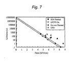
- Time-bias measurements at 350°C taken on 6H n-type SiC MIS capacitors are shown in Figure 7 .
- the measured points are shown by the symbols, and the exponential least squares fit is shown by the lines.
- the lifetimes exhibited by these devices are low, which is partially due to the small sample size. However, these values are not atypical for oxides on n-type SiC at 350°C.
- the ONO capacitors had the highest lifetimes, showing more than an order of magnitude improvement in lifetime over both the deposited and thermal oxides at a given applied electric field.
- the p-type interface quality of ONO capacitors is not as good as the thermal or deposited oxides, the n-type interface quality is better than any of the other materials.
- MISFETs planar metal-insulator semiconductor field effect transistors
- thermal oxidation results in a physical step, as the implanted source and drain regions oxidize faster than the non-implanted channel region. Thermal oxides grown on implanted areas also tend to be weaker than those grown on non-implanted material. These two effects are combined in a thermally oxidized MOSFET, where the step enhances the field and the region of the weakest oxide. Thus the breakdown field of the thermally oxidized MOSFET is significantly reduced from the breakdown fields demonstrated by the MOS capacitors.
- the deposited oxide has a higher breakdown field than the thermally grown oxide, but the highest breakdown voltage was achieved with the ONO dielectric layers.
- the field was slightly low at 350°C, but the breakdown voltage is probably a better indicator of device reliability because a silicon nitride gate insulator must be thicker in order to have the same gate capacitance.
- the ONO structure demonstrated almost double the high temperature breakdown voltage of the thermally oxidized devices.
- the channel mobility of the fat FETs (a "fat" FET has a gate width approximately equal to its gate length) was determined from the linear regime of the MISFET: The drain voltage was set a 0.25 volts, and the gate voltages stepped from 0 to 10 volts in one volt steps. The mobility was calculated from the conductance between the various gate voltages, which is independent of the threshold voltage.
- Figure 5 compares the channel mobility of the MISFETs fabricated with layered ONO dielectrics to those with thermal oxides. The ONO MISFETs have a slightly higher mobility. Figure 5 thus shows that the ONO layered dielectric structure is at least as good as a thermal oxide in these devices.
- An estimate of the MISFET device reliability at high temperatures was measured by applying a gate voltage of 15V (3 MV/cm) to a 4 x 100 ⁇ m gate, grounding the source, drain and substrate, and monitoring the gate current until a compliance current of 1 nA was reached. This compliance current corresponds to a current density of 0.25 mA/cm 2 .
- the gate voltage was increased above the probable use-voltage of 5 V to accelerate this test.
- Table 6 compares the high temperature reliability of the MISFETs fabricated with layered ONO dielectrics with those having thermal and deposited silicon dioxide.
- the ONO MOSFETs have a significantly better high temperature lifetime, e.g., more than a factor of 100x better.
- a packaged MISFET operated successfully for 240 hours. TABLE 6 Device lifetimes at 350°C with a 15 V (3 MV/cm) gate bias Insulator Lifetime Dry Thermal Oxide 0.08 hour Deposited Oxide 0.75 hour ONO > 75 hours ONO (Packaged, Estimated 335°C) 240 hours
- the ONO sample was wafer tested at 350°C for 75 hours without failing. At that point, it was decided to package devices for testing, because the device metals would oxidize if exposed to air for several days at 350°C. The packaged parts were then tested at 350°C. The exact temperature of the packaged devices could not be easily controlled, however, and thus the estimated testing temperature was probably closer to 335°C than to 350°C. Nevertheless, the ONO sample survived for 10 days (240 hours) at 335°C.
- Figure 9 also shows the MISFET lifetimes for comparison with the capacitor results.
- the MISFETs with the dry-wet thermal oxide have a dramatically reduced lifetime when compared with the capacitors. This is most likely due to the physical steps created at the source and drain regions by the accelerated growth of the implanted regions.
- the deposited oxide MISFET failed very close to its projected time, but slightly lower.
- the ONO MISFET fails almost exactly where one would predict from the MIS capacitor data.
- a 4-wafer lot of planar diodes was fabricated.
- a cross section of an exemplary device 50 is shown in Figure 6 .
- the top p-layer 51 was implanted with variable doses.
- a second implant, the Junction Termination Extension (JTE) 52 was performed adjacent to the first implant to reduce field crowding.
- JTE Junction Termination Extension
- the JTE implant helps reduce the field crowding at the edge of the device, a high quality dielectric 53 on the surface of the wafer is required for passivation.
- the shape of the planar diode was circular.
- the dielectric 53 is formed of the oxide/nitride/oxide according to the present invention. Specifically, all three layers were deposited by PECVD.
- the mask set used for this device consisted of diodes with radii varying from 100 to 500 ⁇ m, while the width of the JTE implant varied between 50 and 150 ⁇ m.
- the epitaxial layers should support 5 kV, but the JTE of these devices were designed to block only 3 kV in order to place more stress on the passivation.
- the device performance is more sensitive to the passivation, because the JTE implants do not terminate all of the fields generated by the higher voltage. Accordingly, the passivation must withstand much larger fields.
- the devices were deliberately designed to help evaluate the various dielectric materials.
- n-type substrates for these devices had a 50 ⁇ m epitaxial n - layer doped about 1x10 15 cm -3 grown, and a 1.2 ⁇ m p - layer doped 1x10 18 cm -3 .
- Figure 6 also illustrates the n-type portion of the device at 54, the anode at 55, and the cathode at 56.
- the fabrication of the diode began with etching alignment marks into the SiC wafer for alignment of the future masks.
- the anode junction was defined by etching through the top p-type layer in most of the surface, while leaving circular p-type anode regions exposed.
- a thick (1.4 ⁇ m) oxide mask the regions receiving the low-dose JTE implant were defined.
- the thickness of the oxide mask and the implantation energy and dosage of the p-type dopant (aluminum) were chosen so that only the intended termination region receives the implant while it is blocked entirely from regions where it is not intended.
- the junction region also received this implantation step so that a high surface doping of the p-type layer was formed for ohmic anode contacts.
- the implanted aluminum was annealed to minimize the damage from ion implantation and to electrically activate the implants.
- the breakdown voltage was measured on each type of diode.
- the silicon nitride had a great deal of leakage, and broke down at 2.6 kV.
- the oxide devices had low/no leakage and broke down around 3.5 kV.
- the devices incorporating the dielectric structure of the invention had no leakage out to 5 kV, and broke at a world-record level of 5.9 kV.
- the ONO dielectric of the present invention provides a significant improvement.
- the high temperature lifetime of the ONO layered MISFET is more than a factor of 100x better than the state-of-the-art deposited oxide. This has immediate relevance to high temperature SiC power devices and circuits. By projecting back to the likely rated operating field of 1 MV/cm, it can be predicted that ONO MOSFETs will have a lifetime of more than 240,000 hours at 335°C.
Landscapes
- Insulated Gate Type Field-Effect Transistor (AREA)
- Formation Of Insulating Films (AREA)
- Semiconductor Integrated Circuits (AREA)
- Thyristors (AREA)
- Junction Field-Effect Transistors (AREA)
Applications Claiming Priority (2)
| Application Number | Priority Date | Filing Date | Title |
|---|---|---|---|
| US09/141,795 US6246076B1 (en) | 1998-08-28 | 1998-08-28 | Layered dielectric on silicon carbide semiconductor structures |
| EP99949566A EP1112593A2 (fr) | 1998-08-28 | 1999-08-27 | Structures semi-conductrices stratifiees a dielectrique sur carbure de silicium |
Related Parent Applications (1)
| Application Number | Title | Priority Date | Filing Date |
|---|---|---|---|
| EP99949566.6 Division | 1999-08-27 |
Publications (2)
| Publication Number | Publication Date |
|---|---|
| EP2267760A2 true EP2267760A2 (fr) | 2010-12-29 |
| EP2267760A3 EP2267760A3 (fr) | 2012-08-29 |
Family
ID=22497296
Family Applications (2)
| Application Number | Title | Priority Date | Filing Date |
|---|---|---|---|
| EP99949566A Ceased EP1112593A2 (fr) | 1998-08-28 | 1999-08-27 | Structures semi-conductrices stratifiees a dielectrique sur carbure de silicium |
| EP10178742A Ceased EP2267760A3 (fr) | 1998-08-28 | 1999-08-27 | Dielectrique multicouche sur des structures semi-conductrices en carbure de silicium |
Family Applications Before (1)
| Application Number | Title | Priority Date | Filing Date |
|---|---|---|---|
| EP99949566A Ceased EP1112593A2 (fr) | 1998-08-28 | 1999-08-27 | Structures semi-conductrices stratifiees a dielectrique sur carbure de silicium |
Country Status (9)
| Country | Link |
|---|---|
| US (2) | US6246076B1 (fr) |
| EP (2) | EP1112593A2 (fr) |
| JP (1) | JP5021860B2 (fr) |
| KR (1) | KR100676445B1 (fr) |
| CN (1) | CN1213485C (fr) |
| AU (1) | AU6241199A (fr) |
| CA (1) | CA2340653A1 (fr) |
| TW (1) | TW457627B (fr) |
| WO (1) | WO2000013236A2 (fr) |
Families Citing this family (116)
| Publication number | Priority date | Publication date | Assignee | Title |
|---|---|---|---|---|
| US6972436B2 (en) * | 1998-08-28 | 2005-12-06 | Cree, Inc. | High voltage, high temperature capacitor and interconnection structures |
| US6246076B1 (en) * | 1998-08-28 | 2001-06-12 | Cree, Inc. | Layered dielectric on silicon carbide semiconductor structures |
| JP2001257347A (ja) * | 2000-03-10 | 2001-09-21 | Mitsubishi Electric Corp | 半導体装置及びその製造方法 |
| GB2361244B (en) * | 2000-04-14 | 2004-02-11 | Trikon Holdings Ltd | A method of depositing dielectric |
| US6686616B1 (en) * | 2000-05-10 | 2004-02-03 | Cree, Inc. | Silicon carbide metal-semiconductor field effect transistors |
| US6690042B2 (en) * | 2000-09-27 | 2004-02-10 | Sensor Electronic Technology, Inc. | Metal oxide semiconductor heterostructure field effect transistor |
| US6956238B2 (en) * | 2000-10-03 | 2005-10-18 | Cree, Inc. | Silicon carbide power metal-oxide semiconductor field effect transistors having a shorting channel and methods of fabricating silicon carbide metal-oxide semiconductor field effect transistors having a shorting channel |
| US6767843B2 (en) | 2000-10-03 | 2004-07-27 | Cree, Inc. | Method of N2O growth of an oxide layer on a silicon carbide layer |
| US6610366B2 (en) | 2000-10-03 | 2003-08-26 | Cree, Inc. | Method of N2O annealing an oxide layer on a silicon carbide layer |
| US7067176B2 (en) | 2000-10-03 | 2006-06-27 | Cree, Inc. | Method of fabricating an oxide layer on a silicon carbide layer utilizing an anneal in a hydrogen environment |
| US7192827B2 (en) | 2001-01-05 | 2007-03-20 | Micron Technology, Inc. | Methods of forming capacitor structures |
| US6528373B2 (en) * | 2001-02-12 | 2003-03-04 | Cree, Inc. | Layered dielectric on silicon carbide semiconductor structures |
| EP1265295A3 (fr) * | 2001-06-04 | 2004-05-12 | Matsushita Electric Industrial Co., Ltd. | Diode Schottky en carbure de silicium et procédé pour sa fabrication |
| JP2003017504A (ja) * | 2001-07-03 | 2003-01-17 | Denso Corp | 半導体装置及びその保護膜の膜厚決定方法 |
| JP4492783B2 (ja) * | 2001-09-12 | 2010-06-30 | 日本電気株式会社 | 半導体装置及びその製造方法 |
| WO2003047000A1 (fr) * | 2001-11-30 | 2003-06-05 | Matsushita Electric Industrial Co., Ltd. | Dispositif à semi-conducteur et procédé de fabrication |
| US7033950B2 (en) * | 2001-12-19 | 2006-04-25 | Auburn University | Graded junction termination extensions for electronic devices |
| US6621114B1 (en) * | 2002-05-20 | 2003-09-16 | Advanced Micro Devices, Inc. | MOS transistors with high-k dielectric gate insulator for reducing remote scattering |
| US6521923B1 (en) * | 2002-05-25 | 2003-02-18 | Sirenza Microdevices, Inc. | Microwave field effect transistor structure on silicon carbide substrate |
| US6680130B2 (en) * | 2002-05-28 | 2004-01-20 | Agere Systems, Inc. | High K dielectric material and method of making a high K dielectric material |
| US7880173B2 (en) | 2002-06-28 | 2011-02-01 | National Institute Of Advanced Industrial Science And Technology | Semiconductor device and method of manufacturing same |
| DE10394374B4 (de) * | 2002-06-28 | 2013-02-21 | National Institute Of Advanced Industrial Science And Technology | Halbleitervorrichtung und Verfahren zur Herstellung derselben |
| US7022378B2 (en) * | 2002-08-30 | 2006-04-04 | Cree, Inc. | Nitrogen passivation of interface states in SiO2/SiC structures |
| US7122488B2 (en) * | 2004-03-15 | 2006-10-17 | Sharp Laboratories Of America, Inc. | High density plasma process for the formation of silicon dioxide on silicon carbide substrates |
| US7221010B2 (en) * | 2002-12-20 | 2007-05-22 | Cree, Inc. | Vertical JFET limited silicon carbide power metal-oxide semiconductor field effect transistors |
| US6803071B1 (en) * | 2003-01-10 | 2004-10-12 | The United States Of America As Represented By The Secretary Of The Army | Paraelectric thin film semiconductor material and method for producing the same |
| AU2003211637A1 (en) * | 2003-03-03 | 2004-09-28 | Fujitsu Limited | Mos variable capacitive device |
| JP2004336019A (ja) | 2003-04-18 | 2004-11-25 | Advanced Lcd Technologies Development Center Co Ltd | 成膜方法、半導体素子の形成方法、半導体素子、表示装置の形成方法及び表示装置 |
| US6979863B2 (en) * | 2003-04-24 | 2005-12-27 | Cree, Inc. | Silicon carbide MOSFETs with integrated antiparallel junction barrier Schottky free wheeling diodes and methods of fabricating the same |
| US7074643B2 (en) * | 2003-04-24 | 2006-07-11 | Cree, Inc. | Silicon carbide power devices with self-aligned source and well regions and methods of fabricating same |
| CN101165860B (zh) * | 2003-08-22 | 2010-04-07 | 关西电力株式会社 | 半导体装置及制造方法、使用该半导体装置的电力变换装置 |
| US7138292B2 (en) * | 2003-09-10 | 2006-11-21 | Lsi Logic Corporation | Apparatus and method of manufacture for integrated circuit and CMOS device including epitaxially grown dielectric on silicon carbide |
| US7332795B2 (en) | 2004-05-22 | 2008-02-19 | Cree, Inc. | Dielectric passivation for semiconductor devices |
| US7118970B2 (en) * | 2004-06-22 | 2006-10-10 | Cree, Inc. | Methods of fabricating silicon carbide devices with hybrid well regions |
| US20060226442A1 (en) * | 2005-04-07 | 2006-10-12 | An-Ping Zhang | GaN-based high electron mobility transistor and method for making the same |
| US7414268B2 (en) | 2005-05-18 | 2008-08-19 | Cree, Inc. | High voltage silicon carbide MOS-bipolar devices having bi-directional blocking capabilities |
| US7391057B2 (en) * | 2005-05-18 | 2008-06-24 | Cree, Inc. | High voltage silicon carbide devices having bi-directional blocking capabilities |
| US7615801B2 (en) * | 2005-05-18 | 2009-11-10 | Cree, Inc. | High voltage silicon carbide devices having bi-directional blocking capabilities |
| US20060261346A1 (en) * | 2005-05-18 | 2006-11-23 | Sei-Hyung Ryu | High voltage silicon carbide devices having bi-directional blocking capabilities and methods of fabricating the same |
| US7528040B2 (en) | 2005-05-24 | 2009-05-05 | Cree, Inc. | Methods of fabricating silicon carbide devices having smooth channels |
| US20060267043A1 (en) * | 2005-05-27 | 2006-11-30 | Emerson David T | Deep ultraviolet light emitting devices and methods of fabricating deep ultraviolet light emitting devices |
| JP2007012684A (ja) * | 2005-06-28 | 2007-01-18 | Mitsubishi Electric Corp | 半導体装置とゲート酸化膜の製造方法 |
| US7598576B2 (en) * | 2005-06-29 | 2009-10-06 | Cree, Inc. | Environmentally robust passivation structures for high-voltage silicon carbide semiconductor devices |
| US7855401B2 (en) | 2005-06-29 | 2010-12-21 | Cree, Inc. | Passivation of wide band-gap based semiconductor devices with hydrogen-free sputtered nitrides |
| US7525122B2 (en) * | 2005-06-29 | 2009-04-28 | Cree, Inc. | Passivation of wide band-gap based semiconductor devices with hydrogen-free sputtered nitrides |
| JP5033316B2 (ja) * | 2005-07-05 | 2012-09-26 | 日産自動車株式会社 | 半導体装置の製造方法 |
| US7727904B2 (en) | 2005-09-16 | 2010-06-01 | Cree, Inc. | Methods of forming SiC MOSFETs with high inversion layer mobility |
| US7592211B2 (en) * | 2006-01-17 | 2009-09-22 | Cree, Inc. | Methods of fabricating transistors including supported gate electrodes |
| US7709269B2 (en) | 2006-01-17 | 2010-05-04 | Cree, Inc. | Methods of fabricating transistors including dielectrically-supported gate electrodes |
| US8432012B2 (en) | 2006-08-01 | 2013-04-30 | Cree, Inc. | Semiconductor devices including schottky diodes having overlapping doped regions and methods of fabricating same |
| US7728402B2 (en) * | 2006-08-01 | 2010-06-01 | Cree, Inc. | Semiconductor devices including schottky diodes with controlled breakdown |
| US8710510B2 (en) * | 2006-08-17 | 2014-04-29 | Cree, Inc. | High power insulated gate bipolar transistors |
| US8823057B2 (en) | 2006-11-06 | 2014-09-02 | Cree, Inc. | Semiconductor devices including implanted regions for providing low-resistance contact to buried layers and related devices |
| US8835987B2 (en) | 2007-02-27 | 2014-09-16 | Cree, Inc. | Insulated gate bipolar transistors including current suppressing layers |
| US8067776B2 (en) * | 2007-06-08 | 2011-11-29 | Nissan Motor Co., Ltd. | Method of manufacturing semiconductor device and semiconductor device manufactured thereof |
| US9024327B2 (en) | 2007-12-14 | 2015-05-05 | Cree, Inc. | Metallization structure for high power microelectronic devices |
| JP2009182271A (ja) * | 2008-01-31 | 2009-08-13 | Toshiba Corp | 炭化珪素半導体装置 |
| US8232558B2 (en) | 2008-05-21 | 2012-07-31 | Cree, Inc. | Junction barrier Schottky diodes with current surge capability |
| US8008096B2 (en) * | 2008-06-05 | 2011-08-30 | Intermolecular, Inc. | ALD processing techniques for forming non-volatile resistive-switching memories |
| JP5030172B2 (ja) * | 2008-06-09 | 2012-09-19 | 株式会社神戸製鋼所 | 絶縁膜及びその製造方法、並びに絶縁膜を備えた電子デバイス |
| US8106487B2 (en) | 2008-12-23 | 2012-01-31 | Pratt & Whitney Rocketdyne, Inc. | Semiconductor device having an inorganic coating layer applied over a junction termination extension |
| US8288220B2 (en) * | 2009-03-27 | 2012-10-16 | Cree, Inc. | Methods of forming semiconductor devices including epitaxial layers and related structures |
| US8294507B2 (en) | 2009-05-08 | 2012-10-23 | Cree, Inc. | Wide bandgap bipolar turn-off thyristor having non-negative temperature coefficient and related control circuits |
| CN102422425A (zh) * | 2009-05-11 | 2012-04-18 | 住友电气工业株式会社 | 绝缘栅双极晶体管 |
| US8193848B2 (en) | 2009-06-02 | 2012-06-05 | Cree, Inc. | Power switching devices having controllable surge current capabilities |
| US8629509B2 (en) | 2009-06-02 | 2014-01-14 | Cree, Inc. | High voltage insulated gate bipolar transistors with minority carrier diverter |
| WO2010151857A2 (fr) * | 2009-06-26 | 2010-12-29 | Cornell University | Procédé pour former des structures semi-conductrices iii-v, à passivation par nitrure d'aluminium-silicium |
| US8541787B2 (en) | 2009-07-15 | 2013-09-24 | Cree, Inc. | High breakdown voltage wide band-gap MOS-gated bipolar junction transistors with avalanche capability |
| US8354690B2 (en) | 2009-08-31 | 2013-01-15 | Cree, Inc. | Solid-state pinch off thyristor circuits |
| CN102217070B (zh) * | 2009-09-03 | 2013-09-25 | 松下电器产业株式会社 | 半导体装置及其制造方法 |
| US9117739B2 (en) | 2010-03-08 | 2015-08-25 | Cree, Inc. | Semiconductor devices with heterojunction barrier regions and methods of fabricating same |
| US8415671B2 (en) | 2010-04-16 | 2013-04-09 | Cree, Inc. | Wide band-gap MOSFETs having a heterojunction under gate trenches thereof and related methods of forming such devices |
| JP2011233695A (ja) * | 2010-04-27 | 2011-11-17 | Sharp Corp | ノーマリオフ型GaN系電界効果トランジスタ |
| DE102010031153A1 (de) * | 2010-07-09 | 2012-01-12 | Robert Bosch Gmbh | Feldeffekttransistoren für Gassensoren |
| JP5584823B2 (ja) * | 2011-03-29 | 2014-09-03 | 株式会社日立製作所 | 炭化珪素半導体装置 |
| US9059192B2 (en) * | 2011-04-01 | 2015-06-16 | Himax Technologies Limited | Metal-insulation-metal device |
| US9142662B2 (en) | 2011-05-06 | 2015-09-22 | Cree, Inc. | Field effect transistor devices with low source resistance |
| US9029945B2 (en) | 2011-05-06 | 2015-05-12 | Cree, Inc. | Field effect transistor devices with low source resistance |
| US9396946B2 (en) * | 2011-06-27 | 2016-07-19 | Cree, Inc. | Wet chemistry processes for fabricating a semiconductor device with increased channel mobility |
| US9984894B2 (en) | 2011-08-03 | 2018-05-29 | Cree, Inc. | Forming SiC MOSFETs with high channel mobility by treating the oxide interface with cesium ions |
| JP5628765B2 (ja) * | 2011-08-19 | 2014-11-19 | 株式会社日立製作所 | 半導体装置 |
| WO2013036370A1 (fr) | 2011-09-11 | 2013-03-14 | Cree, Inc. | Module d'alimentation à haute densité de courant comprenant des transistors à topologie améliorée |
| US8618582B2 (en) | 2011-09-11 | 2013-12-31 | Cree, Inc. | Edge termination structure employing recesses for edge termination elements |
| US9640617B2 (en) | 2011-09-11 | 2017-05-02 | Cree, Inc. | High performance power module |
| US8680587B2 (en) | 2011-09-11 | 2014-03-25 | Cree, Inc. | Schottky diode |
| US8664665B2 (en) | 2011-09-11 | 2014-03-04 | Cree, Inc. | Schottky diode employing recesses for elements of junction barrier array |
| US9373617B2 (en) | 2011-09-11 | 2016-06-21 | Cree, Inc. | High current, low switching loss SiC power module |
| GB2495949B (en) * | 2011-10-26 | 2015-03-11 | Anvil Semiconductors Ltd | Silicon carbide epitaxy |
| JP6042160B2 (ja) * | 2012-10-03 | 2016-12-14 | 東京エレクトロン株式会社 | 成膜方法及び成膜装置 |
| US8994073B2 (en) | 2012-10-04 | 2015-03-31 | Cree, Inc. | Hydrogen mitigation schemes in the passivation of advanced devices |
| US9991399B2 (en) | 2012-10-04 | 2018-06-05 | Cree, Inc. | Passivation structure for semiconductor devices |
| US9812338B2 (en) | 2013-03-14 | 2017-11-07 | Cree, Inc. | Encapsulation of advanced devices using novel PECVD and ALD schemes |
| JP2014110402A (ja) * | 2012-12-04 | 2014-06-12 | Rohm Co Ltd | 半導体装置 |
| US9373691B2 (en) * | 2013-08-07 | 2016-06-21 | GlobalFoundries, Inc. | Transistor with bonded gate dielectric |
| CN103681859A (zh) * | 2013-08-27 | 2014-03-26 | 厦门天睿电子有限公司 | 一种碳化硅半导体器件及其制作方法 |
| US9698235B2 (en) | 2013-10-22 | 2017-07-04 | National Institute Of Advanced Industrial Science And Technology | Field-effect transistor |
| US20150255362A1 (en) | 2014-03-07 | 2015-09-10 | Infineon Technologies Ag | Semiconductor Device with a Passivation Layer and Method for Producing Thereof |
| JP2015198185A (ja) * | 2014-04-02 | 2015-11-09 | 東京エレクトロン株式会社 | 成膜方法及び成膜装置 |
| CN103887163B (zh) * | 2014-04-03 | 2016-04-20 | 中国科学院半导体研究所 | 用于SiC基MOS器件栅介质薄膜的制备方法 |
| US10181527B2 (en) * | 2015-10-16 | 2019-01-15 | Samsung Electronics Co., Ltd. | FinFet having dual vertical spacer and method of manufacturing the same |
| JP6701788B2 (ja) * | 2016-02-18 | 2020-05-27 | 富士電機株式会社 | 炭化珪素半導体装置用ゲート絶縁膜の製造方法 |
| CN109478567B (zh) | 2016-07-15 | 2022-12-16 | 罗姆股份有限公司 | 半导体装置 |
| JP6692265B2 (ja) * | 2016-09-16 | 2020-05-13 | 株式会社東芝 | 半導体装置、半導体装置の製造方法、インバータ回路、駆動装置、車両、及び、昇降機 |
| US10355206B2 (en) | 2017-02-06 | 2019-07-16 | Nantero, Inc. | Sealed resistive change elements |
| JP6346341B2 (ja) * | 2017-05-15 | 2018-06-20 | ローム株式会社 | 半導体装置 |
| JP6924166B2 (ja) * | 2018-05-14 | 2021-08-25 | 株式会社東芝 | 半導体装置 |
| DE102019204503B3 (de) | 2018-10-09 | 2020-03-26 | Fraunhofer-Gesellschaft zur Förderung der angewandten Forschung e.V. | Integrierter Kondensator und Verfahren zur Herstellung eines integrierten Kondensators |
| CN111326573A (zh) * | 2018-12-14 | 2020-06-23 | 深圳比亚迪微电子有限公司 | 场效应晶体管及制备方法、电子设备 |
| DE102019120692B4 (de) * | 2019-07-31 | 2025-12-11 | Infineon Technologies Ag | Leistungshalbleitervorrichtung und Verfahren |
| EP3931862B1 (fr) | 2020-03-17 | 2022-10-05 | Hitachi Energy Switzerland AG | Structure de grille isolée, dispositif de puissance utilisant un matériau à large bande interdite comprenant la structure et procédé de fabrication de la structure |
| US12598994B2 (en) | 2021-06-01 | 2026-04-07 | Wolfspeed, Inc. | Multilayer encapsulation for humidity robustness and related fabrication methods |
| US20220384290A1 (en) | 2021-06-01 | 2022-12-01 | Wolfspeed, Inc. | Multilayer encapsulation for humidity robustness and highly accelerated stress tests and related fabrication methods |
| US11842937B2 (en) | 2021-07-30 | 2023-12-12 | Wolfspeed, Inc. | Encapsulation stack for improved humidity performance and related fabrication methods |
| CN116705712A (zh) * | 2022-02-24 | 2023-09-05 | 华为数字能源技术有限公司 | 一种半导体器件及其制造方法 |
| CN117766586B (zh) * | 2023-12-25 | 2024-09-27 | 上海陆芯电子科技有限公司 | 一种应变碳化硅场效应晶体管 |
| CN117976719B (zh) * | 2024-01-29 | 2025-10-17 | 湖北九峰山实验室 | 一种宽禁带半导体器件结构及其制作方法 |
Citations (7)
| Publication number | Priority date | Publication date | Assignee | Title |
|---|---|---|---|---|
| US3924024A (en) * | 1973-04-02 | 1975-12-02 | Ncr Co | Process for fabricating MNOS non-volatile memories |
| US4875083A (en) | 1987-10-26 | 1989-10-17 | North Carolina State University | Metal-insulator-semiconductor capacitor formed on silicon carbide |
| US5506421A (en) | 1992-11-24 | 1996-04-09 | Cree Research, Inc. | Power MOSFET in silicon carbide |
| US5726463A (en) | 1992-08-07 | 1998-03-10 | General Electric Company | Silicon carbide MOSFET having self-aligned gate structure |
| US5763905A (en) | 1996-07-09 | 1998-06-09 | Abb Research Ltd. | Semiconductor device having a passivation layer |
| US9320898B2 (en) | 2012-01-31 | 2016-04-26 | Advanced Bionics Ag | Systems and methods for facilitating apical electrode stimulation by an electro-acoustic stimulation system |
| US9320798B2 (en) | 2010-03-01 | 2016-04-26 | Dicerna Pharmaceuticals, Inc. | Lipid delivery formulations |
Family Cites Families (27)
| Publication number | Priority date | Publication date | Assignee | Title |
|---|---|---|---|---|
| US4466172A (en) | 1979-01-08 | 1984-08-21 | American Microsystems, Inc. | Method for fabricating MOS device with self-aligned contacts |
| JPS61105848A (ja) * | 1984-10-30 | 1986-05-23 | Toshiba Corp | 半導体装置の製造方法 |
| JPS6465870A (en) * | 1987-09-07 | 1989-03-13 | Sharp Kk | Semiconductor element of silicon carbide |
| JPH0766971B2 (ja) | 1989-06-07 | 1995-07-19 | シャープ株式会社 | 炭化珪素半導体装置 |
| JPH04134866A (ja) * | 1990-09-27 | 1992-05-08 | Toshiba Corp | 電界効果トランジスタ装置及びその製造方法 |
| JPH04357879A (ja) * | 1991-06-04 | 1992-12-10 | Sharp Corp | 不揮発性半導体メモリ |
| US5170455A (en) | 1991-10-30 | 1992-12-08 | At&T Bell Laboratories | Optical connective device |
| US5459107A (en) | 1992-06-05 | 1995-10-17 | Cree Research, Inc. | Method of obtaining high quality silicon dioxide passivation on silicon carbide and resulting passivated structures |
| US6344663B1 (en) | 1992-06-05 | 2002-02-05 | Cree, Inc. | Silicon carbide CMOS devices |
| JPH05347299A (ja) * | 1992-06-15 | 1993-12-27 | Seiko Epson Corp | 半導体装置 |
| JP3343160B2 (ja) * | 1992-09-25 | 2002-11-11 | ソニー株式会社 | 液晶表示装置 |
| JP3222234B2 (ja) * | 1992-12-18 | 2001-10-22 | 株式会社リコー | 半導体装置の製造方法 |
| JPH06224416A (ja) * | 1993-01-21 | 1994-08-12 | Nippon Steel Corp | Mos電界効果型トランジスタ及びその製造方法、並びにそのmos電界効果型トランジスタを用いた半導体装置 |
| US5436481A (en) * | 1993-01-21 | 1995-07-25 | Nippon Steel Corporation | MOS-type semiconductor device and method of making the same |
| US5510630A (en) * | 1993-10-18 | 1996-04-23 | Westinghouse Electric Corporation | Non-volatile random access memory cell constructed of silicon carbide |
| JP3429567B2 (ja) * | 1994-07-08 | 2003-07-22 | 株式会社リコー | Mos半導体装置の製造方法 |
| JP3305901B2 (ja) * | 1994-12-14 | 2002-07-24 | 東芝マイクロエレクトロニクス株式会社 | 半導体装置の製造方法 |
| JPH08288500A (ja) * | 1995-04-20 | 1996-11-01 | Hitachi Ltd | 炭化珪素半導体素子とその製造法及び用途 |
| JPH08316226A (ja) * | 1995-05-17 | 1996-11-29 | Sony Corp | 素子分離領域の形成方法及び半導体装置の製造方法 |
| JP3158973B2 (ja) * | 1995-07-20 | 2001-04-23 | 富士電機株式会社 | 炭化けい素縦型fet |
| US5972801A (en) | 1995-11-08 | 1999-10-26 | Cree Research, Inc. | Process for reducing defects in oxide layers on silicon carbide |
| US6002159A (en) | 1996-07-16 | 1999-12-14 | Abb Research Ltd. | SiC semiconductor device comprising a pn junction with a voltage absorbing edge |
| JPH10163338A (ja) * | 1996-11-28 | 1998-06-19 | Ricoh Co Ltd | 半導体装置とその製造方法 |
| SE9704150D0 (sv) * | 1997-11-13 | 1997-11-13 | Abb Research Ltd | Semiconductor device of SiC with insulating layer a refractory metal nitride layer |
| JPH11297712A (ja) * | 1998-04-10 | 1999-10-29 | Sanyo Electric Co Ltd | 化合物膜の形成方法及び半導体素子の製造方法 |
| US6246076B1 (en) * | 1998-08-28 | 2001-06-12 | Cree, Inc. | Layered dielectric on silicon carbide semiconductor structures |
| EP1128443B1 (fr) * | 1998-10-09 | 2009-12-30 | The Kansai Electric Power Co., Inc. | Dispositif semi-conducteur à effet de champ et son procedé de fabrication |
-
1998
- 1998-08-28 US US09/141,795 patent/US6246076B1/en not_active Expired - Lifetime
-
1999
- 1999-08-27 CA CA002340653A patent/CA2340653A1/fr not_active Abandoned
- 1999-08-27 JP JP2000568128A patent/JP5021860B2/ja not_active Expired - Lifetime
- 1999-08-27 CN CNB998114685A patent/CN1213485C/zh not_active Expired - Lifetime
- 1999-08-27 AU AU62411/99A patent/AU6241199A/en not_active Abandoned
- 1999-08-27 TW TW088114720A patent/TW457627B/zh not_active IP Right Cessation
- 1999-08-27 KR KR1020017002565A patent/KR100676445B1/ko not_active Expired - Lifetime
- 1999-08-27 EP EP99949566A patent/EP1112593A2/fr not_active Ceased
- 1999-08-27 EP EP10178742A patent/EP2267760A3/fr not_active Ceased
- 1999-08-27 WO PCT/US1999/019775 patent/WO2000013236A2/fr not_active Ceased
-
2001
- 2001-02-12 US US09/781,732 patent/US6437371B2/en not_active Expired - Lifetime
Patent Citations (7)
| Publication number | Priority date | Publication date | Assignee | Title |
|---|---|---|---|---|
| US3924024A (en) * | 1973-04-02 | 1975-12-02 | Ncr Co | Process for fabricating MNOS non-volatile memories |
| US4875083A (en) | 1987-10-26 | 1989-10-17 | North Carolina State University | Metal-insulator-semiconductor capacitor formed on silicon carbide |
| US5726463A (en) | 1992-08-07 | 1998-03-10 | General Electric Company | Silicon carbide MOSFET having self-aligned gate structure |
| US5506421A (en) | 1992-11-24 | 1996-04-09 | Cree Research, Inc. | Power MOSFET in silicon carbide |
| US5763905A (en) | 1996-07-09 | 1998-06-09 | Abb Research Ltd. | Semiconductor device having a passivation layer |
| US9320798B2 (en) | 2010-03-01 | 2016-04-26 | Dicerna Pharmaceuticals, Inc. | Lipid delivery formulations |
| US9320898B2 (en) | 2012-01-31 | 2016-04-26 | Advanced Bionics Ag | Systems and methods for facilitating apical electrode stimulation by an electro-acoustic stimulation system |
Also Published As
| Publication number | Publication date |
|---|---|
| US6437371B2 (en) | 2002-08-20 |
| WO2000013236A2 (fr) | 2000-03-09 |
| EP2267760A3 (fr) | 2012-08-29 |
| TW457627B (en) | 2001-10-01 |
| KR100676445B1 (ko) | 2007-01-30 |
| CN1213485C (zh) | 2005-08-03 |
| KR20010073055A (ko) | 2001-07-31 |
| JP2002524860A (ja) | 2002-08-06 |
| WO2000013236A9 (fr) | 2001-03-22 |
| US6246076B1 (en) | 2001-06-12 |
| EP1112593A2 (fr) | 2001-07-04 |
| WO2000013236A3 (fr) | 2000-08-24 |
| US20010009788A1 (en) | 2001-07-26 |
| JP5021860B2 (ja) | 2012-09-12 |
| AU6241199A (en) | 2000-03-21 |
| CN1336010A (zh) | 2002-02-13 |
| CA2340653A1 (fr) | 2000-03-09 |
Similar Documents
| Publication | Publication Date | Title |
|---|---|---|
| US6437371B2 (en) | Layered dielectric on silicon carbide semiconductor structures | |
| EP1412970B1 (fr) | Structures de condensateur haute tension haute temperature et leurs procedes de fabrication | |
| US6528373B2 (en) | Layered dielectric on silicon carbide semiconductor structures | |
| Lipkin et al. | Insulator investigation on SiC for improved reliability | |
| US7598576B2 (en) | Environmentally robust passivation structures for high-voltage silicon carbide semiconductor devices | |
| US20040104429A1 (en) | SiC-MISFET and method for fabricating the same | |
| US11222955B2 (en) | Semiconductor power devices having gate dielectric layers with improved breakdown characteristics and methods of forming such devices | |
| EP4333073A1 (fr) | Dispositif électronique à base de sic à diélectrique de grille amélioré et son procédé de fabrication, diode | |
| US11682709B2 (en) | Interface layer control methods for semiconductor power devices and semiconductor devices formed thereof | |
| EP4333027A1 (fr) | Procédé de fabrication de contacts ohmiques d'un dispositif électronique, avec optimisation de budget thermique | |
| Klootwijk et al. | Improvements of deposited interpolysilicon dielectric characteristics with RTP N/sub 2/O-anneal | |
| EP4513567A1 (fr) | Procédé de fabrication d'un dispositif semi-conducteur en carbure de silicium et dispositif semi-conducteur | |
| Suliman et al. | Electrical properties of the gate oxide and its interface with Si in U-shaped trench MOS capacitors: The impact of polycrystalline Si doping and oxide composition | |
| Chao et al. | A Novel Si‐B Diffusion Source for p+‐Poly‐Si Gate |
Legal Events
| Date | Code | Title | Description |
|---|---|---|---|
| PUAI | Public reference made under article 153(3) epc to a published international application that has entered the european phase |
Free format text: ORIGINAL CODE: 0009012 |
|
| AC | Divisional application: reference to earlier application |
Ref document number: 1112593 Country of ref document: EP Kind code of ref document: P |
|
| AK | Designated contracting states |
Kind code of ref document: A2 Designated state(s): AT BE CH CY DE DK ES FI FR GB GR IE IT LI LU MC NL PT SE |
|
| RIN1 | Information on inventor provided before grant (corrected) |
Inventor name: PALMOUR, JOHN, WILLIAMS Inventor name: LIPKIN, LORI, A. |
|
| PUAL | Search report despatched |
Free format text: ORIGINAL CODE: 0009013 |
|
| AK | Designated contracting states |
Kind code of ref document: A3 Designated state(s): AT BE CH CY DE DK ES FI FR GB GR IE IT LI LU MC NL PT SE |
|
| RIC1 | Information provided on ipc code assigned before grant |
Ipc: H01L 29/16 20060101ALN20120723BHEP Ipc: H01L 29/861 20060101ALI20120723BHEP Ipc: H01L 29/51 20060101ALI20120723BHEP Ipc: H01L 21/04 20060101AFI20120723BHEP Ipc: H01L 29/78 20060101ALI20120723BHEP Ipc: H01L 29/94 20060101ALI20120723BHEP |
|
| 17P | Request for examination filed |
Effective date: 20130215 |
|
| 17Q | First examination report despatched |
Effective date: 20140218 |
|
| APBK | Appeal reference recorded |
Free format text: ORIGINAL CODE: EPIDOSNREFNE |
|
| APBN | Date of receipt of notice of appeal recorded |
Free format text: ORIGINAL CODE: EPIDOSNNOA2E |
|
| APBR | Date of receipt of statement of grounds of appeal recorded |
Free format text: ORIGINAL CODE: EPIDOSNNOA3E |
|
| APAV | Appeal reference deleted |
Free format text: ORIGINAL CODE: EPIDOSDREFNE |
|
| APBT | Appeal procedure closed |
Free format text: ORIGINAL CODE: EPIDOSNNOA9E |
|
| STAA | Information on the status of an ep patent application or granted ep patent |
Free format text: STATUS: THE APPLICATION HAS BEEN REFUSED |
|
| 18R | Application refused |
Effective date: 20210216 |