EP4006997A2 - Verfahren zur herstellung einer quantenvorrichtung - Google Patents
Verfahren zur herstellung einer quantenvorrichtung Download PDFInfo
- Publication number
- EP4006997A2 EP4006997A2 EP21209987.3A EP21209987A EP4006997A2 EP 4006997 A2 EP4006997 A2 EP 4006997A2 EP 21209987 A EP21209987 A EP 21209987A EP 4006997 A2 EP4006997 A2 EP 4006997A2
- Authority
- EP
- European Patent Office
- Prior art keywords
- gate
- substrate
- front face
- oxide
- layer
- Prior art date
- Legal status (The legal status is an assumption and is not a legal conclusion. Google has not performed a legal analysis and makes no representation as to the accuracy of the status listed.)
- Granted
Links
Images






Classifications
-
- G—PHYSICS
- G06—COMPUTING OR CALCULATING; COUNTING
- G06N—COMPUTING ARRANGEMENTS BASED ON SPECIFIC COMPUTATIONAL MODELS
- G06N10/00—Quantum computing, i.e. information processing based on quantum-mechanical phenomena
-
- H—ELECTRICITY
- H10—SEMICONDUCTOR DEVICES; ELECTRIC SOLID-STATE DEVICES NOT OTHERWISE PROVIDED FOR
- H10D—INORGANIC ELECTRIC SEMICONDUCTOR DEVICES
- H10D48/00—Individual devices not covered by groups H10D1/00 - H10D44/00
- H10D48/383—Quantum effect devices, e.g. of devices using quantum reflection, diffraction or interference effects
-
- H—ELECTRICITY
- H10—SEMICONDUCTOR DEVICES; ELECTRIC SOLID-STATE DEVICES NOT OTHERWISE PROVIDED FOR
- H10D—INORGANIC ELECTRIC SEMICONDUCTOR DEVICES
- H10D48/00—Individual devices not covered by groups H10D1/00 - H10D44/00
- H10D48/383—Quantum effect devices, e.g. of devices using quantum reflection, diffraction or interference effects
- H10D48/3835—Semiconductor qubit devices comprising a plurality of quantum mechanically interacting semiconductor quantum dots, e.g. Loss-DiVincenzo spin qubits
-
- H—ELECTRICITY
- H10—SEMICONDUCTOR DEVICES; ELECTRIC SOLID-STATE DEVICES NOT OTHERWISE PROVIDED FOR
- H10N—ELECTRIC SOLID-STATE DEVICES NOT OTHERWISE PROVIDED FOR
- H10N60/00—Superconducting devices
- H10N60/01—Manufacture or treatment
-
- H—ELECTRICITY
- H10—SEMICONDUCTOR DEVICES; ELECTRIC SOLID-STATE DEVICES NOT OTHERWISE PROVIDED FOR
- H10N—ELECTRIC SOLID-STATE DEVICES NOT OTHERWISE PROVIDED FOR
- H10N60/00—Superconducting devices
- H10N60/01—Manufacture or treatment
- H10N60/0912—Manufacture or treatment of Josephson-effect devices
-
- H—ELECTRICITY
- H10—SEMICONDUCTOR DEVICES; ELECTRIC SOLID-STATE DEVICES NOT OTHERWISE PROVIDED FOR
- H10N—ELECTRIC SOLID-STATE DEVICES NOT OTHERWISE PROVIDED FOR
- H10N60/00—Superconducting devices
- H10N60/10—Junction-based devices
- H10N60/128—Junction-based devices having three or more electrodes, e.g. transistor-like structures
-
- G—PHYSICS
- G06—COMPUTING OR CALCULATING; COUNTING
- G06N—COMPUTING ARRANGEMENTS BASED ON SPECIFIC COMPUTATIONAL MODELS
- G06N10/00—Quantum computing, i.e. information processing based on quantum-mechanical phenomena
- G06N10/40—Physical realisations or architectures of quantum processors or components for manipulating qubits, e.g. qubit coupling or qubit control
Definitions
- the present invention relates to the field of quantum electronics. It finds for particularly advantageous application the realization of superconducting grids in quantum devices with quantum bits (called quantum bits or qubits), in particular for devices based on architectures with spin qubits or with superconducting qubits.
- quantum bits quantum bits or qubits
- quantum devices with superconducting qubits make it possible in particular to obtain good entanglement between qubits.
- these devices still exhibit too much variability. They are particularly sensitive to small imperfections induced by manufacturing processes. In particular, they require a very high quality interface between the two superconducting reservoirs, to obtain a Josephson effect. It is also difficult to form a unit qubit via these devices.
- Spin-qubit quantum devices can operate with fewer qubits and consume less power. They can also benefit from manufacturing processes and microelectronics technologies to improve the reproducibility and increase the integration density of these spin qubit devices.
- FDSOI fully depleted channel transistor
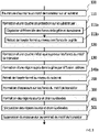
- the figure 1 presents some standard manufacturing steps for such a device.
- One or several transistor patterns each comprising a gate and a gate dielectric are formed 100 on an SOI substrate. Spacers are then formed 200 on either side of the grid patterns.
- the raised source and drain regions are formed 300 by epitaxy at the edge and around the outer spacers. After removal 400 of the hard mask on the top of the grid, the grid is silicided 500.
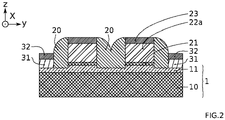
- This method makes it possible in particular to produce a quantum device with two qubits in series, in an active zone 11 of an SOI substrate 1, as illustrated in picture 2 .
- the two gates 22a make it possible to control these two qubits.
- the source and drain regions 31 form reservoirs of charge carriers for these two qubits.
- Such a spin qubit quantum device nevertheless has a lower operating speed than a superconducting qubit device.
- An object of the present invention is to overcome at least in part some of the drawbacks mentioned above.
- an object of the present invention is to provide a method of making a quantum device that reduces power consumption while improving operating speed.
- This lateral diffusion is carried out from the metal layer.
- This metallic layer comprises at least one metallic species capable of forming an alloy or a superconducting compound by reaction after diffusion within the gate. In this case the diffusion is called reactive diffusion. According to one possibility, the metallic species is superconducting before reaction and simply diffuses within the gate.
- a protective layer is advantageously formed at the level of the front face of the substrate.
- the protective layer can thus prevent the diffusion of metallic species from a metallic layer at the surface of the substrate, for example deposited by conformal deposition.
- the protective layer can also prevent the diffusion or the reaction at the surface of the substrate with metallic species originating from metallic residues formed at the end of the lateral diffusion from the flanks of the gate.
- the method according to the invention thus makes it possible to produce a quantum device having a superconducting gate transistor architecture.
- the superconducting region formed by the method according to the invention also makes it possible to reduce the energy consumption of the device during operations on the qubits.
- the invention also relates to a quantum device having a superconducting gate transistor architecture as obtained by the method according to the invention.
- the transistor pattern provided further comprises a hard mask on the top of the gate, said hard mask being configured to prevent diffusion of at least one metal species into the gate from said top, so that the formation of the superconducting region is done only by lateral diffusion from the sides of the gate.
- a hard mask on the top of the gate, said hard mask being configured to prevent diffusion of at least one metal species into the gate from said top, so that the formation of the superconducting region is done only by lateral diffusion from the sides of the gate.
- the metallic layer formed comprises at least one metallic species among cobalt, platinum and vanadium.
- the metallic layer is formed by conformal deposition of metal on the transistor pattern and on the protective layer on the front face of the substrate.
- the metal layer is formed by CVD deposition (acronym for Chemical Vapor Deposition) or by ALD deposition (acronym for Atomic Layer Deposition). This makes it possible to deposit the at least one metallic species on the sides of the grid.
- the metallic layer is formed by PVD deposition (acronym for Physical Vapor Deposition) with conditions allowing redeposition or resputtering (commonly called “sputtering” or “resputtering”) from the bottom of the patterns towards the sides of the grid , typically by plasma treatment.
- the metal layer is formed by non-directional PVD deposition. This makes it possible to deposit the at least one metallic species on the sides of the grid.
- the lateral diffusion is configured to propagate the at least one metallic species from each of the sides of the gate at least to the center of the gate, so that the superconducting region is formed over an entire width L g of the grid.
- the grid is thus totally superconducting. This improves the control of the quantum device thus formed.
- the gate has a width L g ⁇ 40 nm, preferably L g ⁇ 30 nm, preferably L g ⁇ 25 nm, preferably L g ⁇ 20 nm. This reduces the number of entangled qubits in the device.
- the gate has a width L g and the metal layer formed has a thickness e m ⁇ L g /5. This makes it possible to have a sufficient quantity of metallic species in the metallic layer, so that the entire gate can be made superconducting at the end of the lateral diffusion.
- the thickness e m can also depend on the metal used and/or on the nature of the grid.
- the lateral diffusion is done by thermal annealing, for example by RCA type annealing (acronym for Rapid Thermal Annealing).
- the lateral diffusion or lateral silicidation conditions may in particular depend on the metal used and the phase targeted.
- the table below gives examples of the thickness ratio between different metals (Co, Pt and V) and silicon.
- the annealing environment can be under inert gas Ar, He or N 2 .
- the thickness of Si consumed is preferably less than or equal to half the gate width. This makes it possible to avoid forming a polyphase superconducting zone.
- the protective layer formed at the level of the front face of the substrate has a thickness e′ s greater than or equal to 2 nm during the formation of the superconducting region. This makes it possible to improve the sealing of the protective layer with respect to the diffusion of metallic species.
- the differentiated oxidation is carried out from at least one plasma comprising oxygen-based species and hydrogen-based species.
- the hydrogen-based species are taken from dihydrogen H2, ammonia NH3, boron hydride HBr.
- the first plasma succeeds the second plasma.
- the first plasma is a hydrogen H2 plasma and the second plasma is an oxygen O2 plasma.
- the first and second plasmas are carried out simultaneously from an HBr/O2 plasma chemistry. This reduces the number of steps. Additionally, HBr/O2 plasma chemistry can be used to etch and form the transistor pattern. The steps of supplying the transistor pattern and of forming the protective layer can therefore be partly merged.
- the removal of the oxide formed at the flanks of the gate is done by wet etching.
- the sides of the gate are exposed over at least 90% of their height h g , after removal of the deposited oxide.
- the oxide deposition is carried out by centrifugation.
- the substrate carries a plurality of transistor patterns.
- a subset of the plurality of transistor patterns is masked before the formation of the metallic layer so as to avoid the formation of superconducting regions in the gates of the transistor patterns of said subset.
- a hard mask on a grid does not necessarily mean that the hard mask and the grid are directly in contact with each other, but it does mean that the hard mask at least partially covers the grid by being either directly in contact with it or by being separated from it by at least one other layer or at least one other element.
- a layer can also be composed of several sub-layers of the same material or of different materials.
- a substrate, a layer, a device, "based" on a material M is understood to mean a substrate, a layer, a device comprising only this material M, or this material M and possibly other materials, for example alloying elements, impurities or doping elements.
- a spacer based on silicon nitride SiN can for example comprise non-stoichiometric silicon nitride (SiN), or stoichiometric silicon nitride (Si3N4), or else a silicon oxy-nitride (SiON).
- a spacer forms a ring around the grid, with a closed contour; the description of a spacer preferably means this single spacer around the grid; however, the sectional illustrative drawings, generally along a plane parallel to the longitudinal direction of the channel, show two spacer portions on either side of the sides of the grid. By extension, these two spacer parts are often referred to as “the spacers”. This latter terminology may optionally be adopted in this application. Furthermore, the invention extends to embodiments in which at least two discontinuous spacers cover a grid pattern.
- the present invention notably allows the fabrication of at least one quantum device or of a plurality of quantum devices on a substrate.
- This substrate can be solid or “bulk” according to the English terminology, or even of the semiconductor on insulator type, for example a silicon on insulator SOI substrate (acronym for “silicon on insulator”) or a germanium on insulator substrate GeOI (acronym for “germanium on insulator”).
- the invention can also be implemented more broadly for various microelectronic devices or components.
- microelectronic device any type of element made with the means of microelectronics.
- These devices include in particular, in addition to devices for purely electronic purposes, micromechanical or electromechanical devices (MEMS, NEMS, etc.) as well as optical or optoelectronic devices (MOEMS, etc.).
- MEMS micromechanical or electromechanical devices
- MOEMS optical or optoelectronic devices
- successive steps of the manufacturing process are described below.
- the adjective “successive” does not necessarily imply, even if this is generally preferred, that the stages follow each other immediately, intermediate stages possibly separating them.
- the term “step” means the performance of part of the method, and can designate a set of sub-steps.
- the step of forming the protective layer can occur partly at the end of the step of supplying the transistor pattern, so that these two steps are partly coincident.
- This is for example the case when a plasma in HBr/O2 chemistry is used to etch and form the transistor pattern.
- This plasma can be extended, preferably by varying the conditions of said plasma, so as to form the protective layer.
- dielectric describes a material whose electrical conductivity is low enough in the given application to serve as an insulator.
- a dielectric material preferably has a dielectric constant of less than 7.
- the spacers are typically formed from a dielectric material.
- selective etching with respect to or “etching having selectivity with respect to” an etching configured to remove a material A or a layer A with respect to a material B or d layer B, and having an etching speed of material A greater than the etching speed of material B.
- the selectivity is the ratio between the etching speed of material A over the etching speed of material B.
- thickness for a layer is taken according to a direction normal to the main extension plane of the layer, the height and the depth are taken according to a direction normal to the base plane of the substrate.
- the main extension plane of the layer is generally parallel to a lower face or an upper face of this layer, respectively of this substrate.
- a preferably orthonormal reference frame formed by the x, y, z axes is shown in the accompanying drawings.
- the substrate more precisely its lower face and/or its upper face, extend in the basal plane xy.
- the length is taken in the direction carried by the x axis, called the longitudinal axis
- the width is taken in the direction carried by the y axis.
- An element located "straight” or “straight” to another element means that these two elements are both located on the same line perpendicular to the basal plane, or on the same line oriented along the z axis on the figures.
- “Horizontal” means an orientation parallel to an xy plane. “Vertical” means an orientation parallel to the z axis.
- a direction substantially normal to a plane means a direction having an angle of 90 ⁇ 10° relative to the plane.
- a first embodiment of the method is illustrated in figure 3 and 4Y-4J .
- This first embodiment makes it possible to form a quantum device with at least two qubits, these qubits being electron spin qubits or superconducting qubits.
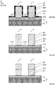
- Two transistor patterns 2 each comprising a gate dielectric 21, a gate 22a and a hard mask 40 stacked on a substrate 1 are provided 100 ( figure 4A ).
- the substrate 1 is typically here an SOI substrate comprising an active region 11 on a buried oxide 10.
- the gate dielectric 21 is typically based on silicon dioxide SiO2, or based on a material with a high dielectric constant.
- Gate dielectric 21 typically has a thickness e g of between 1 nm and 5 nm.
- Gate 22a is typically based on polycrystalline silicon (polySi).
- Gate 22a typically has a width L g of less than 25 nm and a height h g of between 20 nm and 150 nm.
- the hard mask 40 is typically based on silicon nitride SiN or SiO2.
- the device is produced on a bulk silicon substrate.
- a dopant introduction step can be provided to ensure confinement of the electron, and/or dielectric materials, other than silicon oxide, can be provided. These dielectrics are based, for example, on nitride or alumina.
- the supply 100 of the two patterns of transistors 2 corresponds here to the formation of these patterns of transistors 2.
- the gates 22a are etched by conventional plasma etching, for example using a plasma in HBr/O2 chemistry.
- the formation 110 of a protective layer 111 ( figure 4B ) at the level of the front face 101 of the substrate 1 can be done from an overetching step directly following the etching of the gates 22a. This step of overetching aims to achieve a differentiated oxidation 111a of the sides 221 and of the front face 101.
- each gate 22a are oxidized over a thickness ef to form the oxide 222 ( figure 4B ).
- the front face is oxidized over a thin layer to form the oxide 111 ( figure 4B ).
- the differentiated oxidation 111a is configured so that the thickness e f of the oxide 222 is strictly less, for example at least 20% less and preferably at least 50% less, than the thickness e s of the oxide 111.
- the thickness e f of the oxide 222 can be between 1 nm and 4 nm.
- the thickness e s of the oxide 111 can be between 3 nm and 10 nm.
- the HBr/O2 chemistry plasma used to etch the gates 22a is adapted to oxidize the sides 221 and the front face 101 in a differentiated manner at the end of the etching of the gates 22a.
- the HBr/O2 mixture is 40:1 (eg 200 sccm HBr to 5 sccm O2).
- the pressure is less than 50 mTorr, preferably less than 10 mTorr (eg 6 mTorr).
- the source power is greater than 200 W, preferably greater than 400 W (typically 500 W).
- the bias voltage is greater than 50 V, preferably greater than 60 V (typically 80 V).
- the temperature of the substrate is between 50°C and 70°C, preferably around 60°C.
- the overetching step is carried out sequentially by a first plasma based on hydrogen, for example based on dihydrogen H2 or ammonia NH3, followed by a second plasma based on oxygen O2.
- the first plasma here makes it possible to modify both the material of the active layer 11 over a depth d s from the front face 101, and the material of the gate 22a over a width d f from the sides 221.
- the portions modified by this first plasma are not etched.
- This first plasma is configured so that the width d f is strictly less, for example at least 20% less and preferably at least 50% less, than the depth d s .
- the width d f can be between 1 nm and 4 nm.
- the depth d s can be between 3 nm and 10 nm.
- the second plasma makes it possible to preferentially oxidize the portions of active layer 11 and gate 22a modified by the first plasma.
- This makes it possible to form the oxide 111 with a thickness e s and the oxide 222 with a thickness e f .
- the oxide formed by oxidation of the silicon can be larger than the silicon consumed during the oxidation.
- the oxide 111 can typically extend under the front face 101 and above the front face 101, so that the depth d s is not necessarily equal to the thickness e s .
- a thin oxide 222 is formed on the sides 221 of the gate 22a and a thick oxide 111 is formed on the front face 101 of the active layer 11.
- the next step consists in removing 111b the fine oxide 222 on the sides 221 of the gate 22a ( Fig. 4C ).
- This removal 111b can be done by wet etching, for example based on dilute hydrofluoric acid dHF (HF concentration of the order of 0.1% to 1%).
- this withdrawal 111b is done by a process of the SiCoNi TM type, which typically comprises a delocalized plasma based on an NF3/NH3 mixture followed by sublimation annealing.
- part of the oxide 111 on the front face is retained and has a thickness e′ s ⁇ e s .
- This part of oxide 111 forms the protective layer 111 of thickness e′ s ( Fig. 4C ).
- the thickness e' s is greater than or equal to 2 nm.
- the sides 221 of the grid 22a are again exposed.
- the sides 221 can be cleaned, for example by argon or helium plasma, before depositing a metallic layer 50.
- the metallic layer 50 can be deposited conformally on the transistor patterns 2 and on the layer protection 111 ( 4D figure ).
- the metallic layer 50 notably covers the sides 221.
- This metallic layer 50 comprises at least one superconducting element, for example taken from cobalt, platinum or vanadium. It has a thickness e m . This thickness e m is preferably chosen so that the entire gate 22a is transformed into a superconducting region at the end of the next step of lateral diffusion.
- the width L supra required to transform the gate 22a into a superconducting region is equal to L g /2.
- a thickness e m of metal layer 50 greater than or equal to the width L si of polySi consumed during the transformation makes it possible to silicide the gate 22a over its entire width L g .
- We will therefore preferably choose e m ⁇ L g /2 ⁇ , ie e m ⁇ L g /5.
- the formation 120 of the superconducting region 22b within the gate 22a takes place by lateral diffusion of the metallic species from the flanks 221, that is to say mainly along y.
- This lateral diffusion is preferably configured so that the superconducting region 22b is formed over the entire width L g of the gate 22a ( Figure 4E ).
- two diffusion fronts develop from the two respective sides of the gate 22a. These diffusion fronts are substantially vertical and progress in the direction of the median plane xz of the gate 22a.
- the grid 22a is completely transformed into a superconducting region 22b when the fronts meet at the level of this median plane xz.
- the presence of the hard mask 40 advantageously prevents a diffusion of metallic species from the top of the grid 22a.
- the crystal quality of the superconducting region 22b formed by lateral joining of two diffusion fronts is better than the crystal quality of a superconducting region 22b formed by joining three fronts.
- the diffusion of the metallic species within the gate 22a is typically done by thermal annealing, for example at a temperature of 400 to 800°C. Diffusion conditions typically depend on the metal species chosen and its reactivity with silicon. Examples are provided in the table presented above.
- the protective layer 111 prevents the metallic species from diffusing into the active layer 11.
- the metallic residues are preferably cleaned, for example using a solution based on hydrogen peroxide H2O2 such as Caro (H 2 O 2 :H 2 SO4), aqua regia (HCl:HNO3) and/or SC1 (H 2 O:H 2 O 2 :NH 4 OH).
- the protective layer 111 can then be removed 140a so as to expose the active layer 11 ( figure 4F ).
- This withdrawal 140a can be done by wet etching, for example based on hydrofluoric acid HF.
- the removal 140a of this protective layer 111 is done before the step 300 of epitaxy of the source and drain regions.
- This withdrawal can therefore be carried out directly after formation 130 of the superconducting region 22b, or subsequently, for example after formation 200 of the spacers. This last possibility can in particular improve the quality of the interface between the active layer 11 and the future spacer 20.
- the spacer or spacers 20 are formed 200 on either side of the grid patterns.
- the formation of SiN-based spacers 20 is a perfectly known standard step.
- the source and drain regions 31 are then formed 300 around the spacers 20 ( figure 4H ) exteriors. These regions 31 are typically formed by epitaxy along z from the exposed zones of the active layer 11. This makes it possible to obtain, in a known way, raised source and drain regions 31, also called RSD (for Raised Source Drain).
- a standard silicidation 401 of the source and drain regions 31 can then be carried out to form silicided portions 32 ( Fig. 4I ).
- the hard mask 40 is kept on top of the superconducting region 22b so as to avoid additional silicidation of the superconducting region 22b.
- the hard mask 40 can be removed 501 after silicidation of the source and drain regions 31, so as to expose the top of the superconducting region 22b, as illustrated in FIG. figure 4J .
- a two-qubit quantum device comprising at least two superconducting regions 22b is thus advantageously formed.
- FIG. 5 and 6A-6J A second embodiment of the method is illustrated in figure 5 and 6A-6J .
- This second embodiment also makes it possible to form a quantum device with two qubits, these qubits being electron spin qubits or superconducting qubits.
- the formation 110 of the protective layer differs from the previous embodiment. Only the different characteristics of the first embodiment are described below, the other characteristics not described being deemed identical.
- Two patterns of transistors 2 each comprising a gate dielectric 21, a gate 22a and a hard mask 40 stacked on a substrate 1 are provided here 100 ( Figure 6A ) independently of the step 110 of forming the protective layer.
- the formation 110 of the protective layer begins here after the etching of the gates 22a.
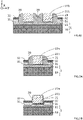
- This formation 110 is typically done in two steps: an oxide layer 60 is first formed between the transistor patterns 2, on the front face 101, as illustrated at figure 6B .
- This layer of oxide 60 for example a fluid oxide of the SoG type (acronym for Spin on Glass), can be deposited 112a by centrifugation.
- the deposition conditions by centrifugation can be chosen according to the density of transistor patterns 2 on the substrate, the height/width aspect ratio of the spaces to be filled, and the thickness of oxide 60 desired. in a known manner, the speed of the spinner will be adapted for a homogeneous deposition over the entire plate as well as the process time to control the thickness deposited. Annealing then makes it possible to solidify the oxide layer 60.
- a partial removal 112b of this oxide layer 60 is then performed so as to form a protective layer 112 of thickness e s ( Fig. 6C ).
- This recess 112b is preferably configured so that the thickness e s of the protective layer 112 is greater than 2 nm and/or greater than the thickness e g of the gate dielectric 21. This makes it possible to avoid any subsequent parasitic diffusion of metal in the active layer 11, in particular at the level of the foot of the transistor patterns, directly above the flanks 221.
- This partial removal 112b can be performed by wet etching based on HF or by plasma etching in fluorocarbon chemistry. A dilute HF solution of the order of 0.1% to 1% is preferably used. This makes it possible to obtain good etching selectivity with respect to the gate 22a and/or the hard mask 40.
- the removal 112b can also be done by a process of the SiCoNi TM type, which typically comprises a delocalized plasma based of an NF3/NH3 mixture followed by sublimation annealing.
- the sides 221 of the grid 22a are partially exposed after this withdrawal 112b, over at least 80% of their height h g , and preferably over at least 90% of their height h g .
- the metallic layer 50 is then deposited 120 on the exposed flanks 221 of the transistor patterns, as illustrated in figure 6D .
- the lateral diffusion of the superconducting elements then takes place from the sides 221 covered by the metallic layer 50, so as to form 130 the superconducting region 22b, as previously ( Figure 6E ).
- the metal residues are preferably cleaned, then the protective layer 112 is removed 140b so as to expose the front face 101 of the active layer 11 ( figure 6F ).
- This second embodiment thus makes it possible to maintain a thickness of active layer 11 that is substantially constant. This makes it possible to maintain a sufficient active layer thickness, typically greater than 3 nm. Such a thickness of active layer makes it possible to avoid phenomena of agglomeration or balling of the active layer during subsequent processes at high temperatures, for example during the epitaxy of raised sources and drains RSD.
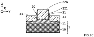
- Figures 7A, 7B , 7C as well as Figures 8A-8F and 9A-9D illustrate some of these embodiments in a non-limiting manner.
- the width of the spacers 20 can also be reduced, so as to bring the source and drain regions 31 closer to the channel (conventionally located under the superconducting region 22b).
- the standard silicide 32 of the source and drain regions 31 can be replaced by a superconducting silicide 33, for example of the same nature as the superconducting region 22b ( Fig. 7C ).
- This can be interesting for some applications, for example for transmon (superconducting charge qubit), gatemon (transmon with variable bias) or even JoFET (FET with superconducting source and drain regions) applications.
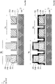
- the figures 8A to 8F illustrate part of the method making it possible to co-integrate on a same substrate 1 conventional MOSFET FDSOI transistors and quantum devices with a superconducting gate.
- This can be achieved by masking with a masking layer 70 part of the patterns of transistors 2 before the formation 120 of the metallic layer 50.
- This makes it possible to avoid the formation 130 of superconducting regions 22b in the gates 22a of the patterns of transistors 2 masked.
- a step of conventional photolithography makes it possible to mask part of the patterns of transistors 2 by a resin 71 ( figure 8B ).
- the masking layer 70 is then removed from the unmasked transistor patterns 2, for example by wet process from an HF solution or by isotropic plasma.
- Resin 71 is then removed, by wet process or by O2 plasma, so as to obtain a first set 2a of patterns of transistors 2 with masking layer 70, and a second set 2b of patterns of transistors 2 without masking layer 70 ( Fig. 8C ).
- the metallic layer 50 can then be deposited conformally on the first and second assemblies 2a, 2b, as illustrated in figure 8D .
- the formation 130 of the superconducting regions 22b then takes place only within the gates 22a of the second set 2b of transistor patterns 2, as shown in figure 8E .
- the masking layer 70 advantageously prevents the lateral diffusion of the superconducting elements within the gates 22a of the first set 2a of patterns of transistors 2.
- the gates 22a of the first set 2a of patterns of transistors 2 are thus preserved.
- the masking layer 70 can then be removed, as shown in figure 8F . This removal can be done by wet etching based on a solution of phosphoric acid H3PO4 if the masking layer 70 is based on SiN. Such an etching notably has good selectivity with respect to the oxide 111, 112.
- isotropic plasma etching can be performed to remove the masking layer 70.
- a wet etching based on an HF solution can alternatively be carried out if the masking layer 70 is based on SiO2.
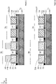
- the figures 9A to 9D illustrate part of the process for siliciding the gates 22a of conventional FDSOI MOSFET transistors co-integrated with superconducting gate quantum devices.
- the active layer 11 illustrated here is of constant thickness.
- the source and drain regions can here be formed directly in the active layer 11.
- This part of the method can also be implemented with raised source and drain regions, for example formed on an active layer 11 of non-constant thickness, such as described and illustrated previously.
- the hard mask 40 is removed from the top of the gates 22a of the set 2a, and kept on the top of the superconducting gates 22b of the set 2b ( figure 9A ).
- a metal layer 51 for example based on nickel or titanium, can then be deposited conformally on the patterns of the sets 2a, 2b ( Figure 9B ).
- Silicidation can then be carried out, typically by thermal annealing, so as to partially or totally silicide the gates 22a, 23 of the assembly 2a ( figure 9C ).
- This siliciding does not affect the superconducting gates 22b of the assembly 2b, which are protected by the spacers 20 and the hard masks 40.
- This siliciding can also make it possible to form silicided portions 32 at the level of the source and drain regions.
- quantum devices with a superconducting gate 22b and MOSFET FDSOI transistors with a non-superconducting silicide gate 23 are co-integrated on a same substrate 1 ( figure 9D ).
Landscapes
- Engineering & Computer Science (AREA)
- Physics & Mathematics (AREA)
- Theoretical Computer Science (AREA)
- General Physics & Mathematics (AREA)
- Manufacturing & Machinery (AREA)
- Data Mining & Analysis (AREA)
- General Engineering & Computer Science (AREA)
- Condensed Matter Physics & Semiconductors (AREA)
- Mathematical Analysis (AREA)
- Mathematical Optimization (AREA)
- Pure & Applied Mathematics (AREA)
- Computing Systems (AREA)
- Evolutionary Computation (AREA)
- Mathematical Physics (AREA)
- Software Systems (AREA)
- Computational Mathematics (AREA)
- Artificial Intelligence (AREA)
- Superconductor Devices And Manufacturing Methods Thereof (AREA)
- Insulated Gate Type Field-Effect Transistor (AREA)
- Thin Film Transistor (AREA)
Applications Claiming Priority (1)
| Application Number | Priority Date | Filing Date | Title |
|---|---|---|---|
| FR2012305A FR3116946B1 (fr) | 2020-11-27 | 2020-11-27 | Procédé de réalisation d’un dispositif quantique |
Publications (3)
| Publication Number | Publication Date |
|---|---|
| EP4006997A2 true EP4006997A2 (de) | 2022-06-01 |
| EP4006997A3 EP4006997A3 (de) | 2022-06-15 |
| EP4006997B1 EP4006997B1 (de) | 2023-10-25 |
Family
ID=74554004
Family Applications (1)
| Application Number | Title | Priority Date | Filing Date |
|---|---|---|---|
| EP21209987.3A Active EP4006997B1 (de) | 2020-11-27 | 2021-11-23 | Verfahren zur herstellung einer quantenvorrichtung |
Country Status (3)
| Country | Link |
|---|---|
| US (1) | US11941485B2 (de) |
| EP (1) | EP4006997B1 (de) |
| FR (1) | FR3116946B1 (de) |
Family Cites Families (9)
| Publication number | Priority date | Publication date | Assignee | Title |
|---|---|---|---|---|
| DE69117628T2 (de) * | 1990-09-10 | 1996-09-26 | Sumitomo Electric Industries | Supraleitende Einrichtung mit einer reduzierten Dicke der supraleitenden Schicht und Methode zu deren Herstellung |
| FR3066297B1 (fr) | 2017-05-11 | 2019-06-14 | Commissariat A L'energie Atomique Et Aux Energies Alternatives | Dispositif quantique a qubits de spin |
| FR3068518B1 (fr) | 2017-06-28 | 2019-08-30 | Commissariat A L'energie Atomique Et Aux Energies Alternatives | Procede de controle d'un dispositif quantique a qubit de spin |
| WO2019002761A1 (fr) | 2017-06-28 | 2019-01-03 | Commissariat A L'energie Atomique Et Aux Energies Alternatives | Procede de controle d'un dispositif quantique a qubit de spin |
| FR3072375B1 (fr) | 2017-10-18 | 2021-04-16 | Commissariat Energie Atomique | Dispositif quantique a qubits de spin couples de maniere modulable |
| US11482614B2 (en) * | 2017-12-23 | 2022-10-25 | Intel Corporation | Quantum dot devices |
| FR3078441B1 (fr) | 2018-02-27 | 2020-03-20 | Commissariat A L'energie Atomique Et Aux Energies Alternatives | Dispositif quantique comprenant des transistors fet et des qubits co-integres sur un meme substrat |
| FR3088483B1 (fr) * | 2018-11-14 | 2022-01-14 | Commissariat Energie Atomique | Transistor a blocs de source et de drain siliciures proches du canal |
| FR3116947B1 (fr) * | 2020-11-27 | 2022-11-18 | Commissariat Energie Atomique | Dispositif quantique et son procédé de réalisation |
-
2020
- 2020-11-27 FR FR2012305A patent/FR3116946B1/fr active Active
-
2021
- 2021-11-23 EP EP21209987.3A patent/EP4006997B1/de active Active
- 2021-11-24 US US17/456,388 patent/US11941485B2/en active Active
Non-Patent Citations (1)
| Title |
|---|
| S. DE FRANCESCHI ET AL.: "SOI technology for quantum information processing", ELECTRON DEVICES MEETING (IEDM, 2016, pages 1 - 4 |
Also Published As
| Publication number | Publication date |
|---|---|
| FR3116946B1 (fr) | 2022-11-11 |
| EP4006997A3 (de) | 2022-06-15 |
| FR3116946A1 (fr) | 2022-06-03 |
| EP4006997B1 (de) | 2023-10-25 |
| US20220172093A1 (en) | 2022-06-02 |
| US11941485B2 (en) | 2024-03-26 |
Similar Documents
| Publication | Publication Date | Title |
|---|---|---|
| EP2096676A1 (de) | Verfahren zur Herstellung einer Halbleitervorrichtung mit vergrabenem Gitter und entsprechende integrierte Halbleiterschaltung | |
| EP1091417A1 (de) | Herstellungsverfahren für Halbleiterbauelement mit Rundherum-Gate und dadurch hergestelltes Bauelement | |
| EP0426251A1 (de) | Verfahren zur Herstellung eines MIS-Transistor-Bauelementes mit einer invertierten T-förmigen Gitterelektrode | |
| FR2823010A1 (fr) | Procede de fabrication d'un transistor vertical a grille isolee a quadruple canal de conduction, et circuit integre comportant un tel transistor | |
| FR2886761A1 (fr) | Transistor a canal a base de germanium enrobe par une electrode de grille et procede de fabrication d'un tel transistor | |
| FR3025938A1 (fr) | Realisation d'espaceurs au niveau de flancs d'une grille de transistor | |
| WO2014037410A1 (fr) | Procédé de gravure d'un matériau semiconducteur cristallin par implantation ionique puis gravure chimique à base de chlorure d'hydrogène | |
| FR2891664A1 (fr) | Transistor mos vertical et procede de fabrication | |
| EP4006996B1 (de) | Quantenvorrichtung und ihr herstellungsverfahren | |
| EP4006997B1 (de) | Verfahren zur herstellung einer quantenvorrichtung | |
| FR2881575A1 (fr) | Transistor mos a grille totalement siliciuree | |
| EP1433206B1 (de) | Ein-elektron-transistor mit einem vertikalkanal, und herstellungsverfahren dafür | |
| EP0904599B1 (de) | VERFAHREN ZUM ÄTZEN DES GATES IN MOS TECHNOLOGIE UNTER VERWENDUNG EINER HARTEN MASKE AUF DER BASIS VON SiON | |
| EP3136429B1 (de) | Herstellung von ohmschen kontakten für eine vorrichtung, die einen bereich aus iii-v-halbleitermaterial und einen bereich aus einem anderen halbleitermaterial enthält | |
| FR2844396A1 (fr) | Procede de realisation d'un composant electronique integre et dispositif electrique incorporant un composant integre ainsi obtenu | |
| EP3859769B1 (de) | Verfahren zum ätzen im nanometerbereich einer germanium-zinn-legierung (gesn) für fet-transistor | |
| EP4185093B1 (de) | Verfahren zur herstellung einer quantenvorrichtung | |
| EP4002482B1 (de) | Verfahren zur herstellung eines bereichs, der mit einer mikroelektronischen vorrichtung dotiert ist | |
| FR2805924A1 (fr) | Procede de gravure d'une couche de silicium polycristallin et son application a la realisation d'un emetteur auto- aligne avec la base extrinseque d'un transistor bipolaire simple ou double polysilicium | |
| WO2012049071A1 (fr) | Transistor a effet de champ sur ilot de materiau semiconducteur auto-assemble | |
| EP4506991A1 (de) | Verfahren zur herstellung einer mikroelektronischen vorrichtung auf der basis eines halbmetall-materials | |
| WO2025108884A1 (fr) | Procede de fabrication de super reseaux doubles obtenus par transfert de couche | |
| EP4002486A1 (de) | Verfahren zur herstellung eines mit einer mikroelektronischen vorrichtung dotierten bereichs | |
| EP4053884A1 (de) | Verfahren zum ätzen einer dielektrischen dreidimensionalen schicht | |
| FR3098978A1 (fr) | procédé de fabrication de transistors |
Legal Events
| Date | Code | Title | Description |
|---|---|---|---|
| PUAI | Public reference made under article 153(3) epc to a published international application that has entered the european phase |
Free format text: ORIGINAL CODE: 0009012 |
|
| STAA | Information on the status of an ep patent application or granted ep patent |
Free format text: STATUS: REQUEST FOR EXAMINATION WAS MADE |
|
| PUAL | Search report despatched |
Free format text: ORIGINAL CODE: 0009013 |
|
| 17P | Request for examination filed |
Effective date: 20211123 |
|
| AK | Designated contracting states |
Kind code of ref document: A2 Designated state(s): AL AT BE BG CH CY CZ DE DK EE ES FI FR GB GR HR HU IE IS IT LI LT LU LV MC MK MT NL NO PL PT RO RS SE SI SK SM TR |
|
| AK | Designated contracting states |
Kind code of ref document: A3 Designated state(s): AL AT BE BG CH CY CZ DE DK EE ES FI FR GB GR HR HU IE IS IT LI LT LU LV MC MK MT NL NO PL PT RO RS SE SI SK SM TR |
|
| RIC1 | Information provided on ipc code assigned before grant |
Ipc: G06N 10/00 20220101ALI20220509BHEP Ipc: H01L 39/22 20060101AFI20220509BHEP |
|
| REG | Reference to a national code |
Ref country code: DE Ref legal event code: R079 Free format text: PREVIOUS MAIN CLASS: H01L0039220000 Ipc: H10N0060100000 Ref country code: DE Ref legal event code: R079 Ref document number: 602021006194 Country of ref document: DE Free format text: PREVIOUS MAIN CLASS: H01L0039220000 Ipc: H10N0060100000 |
|
| REG | Reference to a national code |
Ref country code: DE Ref legal event code: R079 Free format text: PREVIOUS MAIN CLASS: H10N0060100000 Ipc: H10N0060010000 Ref country code: DE Ref legal event code: R079 Ref document number: 602021006194 Country of ref document: DE Free format text: PREVIOUS MAIN CLASS: H10N0060100000 Ipc: H10N0060010000 |
|
| RIC1 | Information provided on ipc code assigned before grant |
Ipc: G06N 10/00 20220101ALI20230412BHEP Ipc: H10N 60/10 20230101AFI20230412BHEP |
|
| GRAP | Despatch of communication of intention to grant a patent |
Free format text: ORIGINAL CODE: EPIDOSNIGR1 |
|
| STAA | Information on the status of an ep patent application or granted ep patent |
Free format text: STATUS: GRANT OF PATENT IS INTENDED |
|
| RIC1 | Information provided on ipc code assigned before grant |
Ipc: G06N 10/00 20220101ALI20230425BHEP Ipc: H10N 60/10 20230101ALI20230425BHEP Ipc: H10N 60/01 20230101AFI20230425BHEP |
|
| INTG | Intention to grant announced |
Effective date: 20230519 |
|
| GRAS | Grant fee paid |
Free format text: ORIGINAL CODE: EPIDOSNIGR3 |
|
| GRAA | (expected) grant |
Free format text: ORIGINAL CODE: 0009210 |
|
| STAA | Information on the status of an ep patent application or granted ep patent |
Free format text: STATUS: THE PATENT HAS BEEN GRANTED |
|
| AK | Designated contracting states |
Kind code of ref document: B1 Designated state(s): AL AT BE BG CH CY CZ DE DK EE ES FI FR GB GR HR HU IE IS IT LI LT LU LV MC MK MT NL NO PL PT RO RS SE SI SK SM TR |
|
| REG | Reference to a national code |
Ref country code: GB Ref legal event code: FG4D Free format text: NOT ENGLISH |
|
| REG | Reference to a national code |
Ref country code: CH Ref legal event code: EP |
|
| REG | Reference to a national code |
Ref country code: DE Ref legal event code: R096 Ref document number: 602021006194 Country of ref document: DE |
|
| REG | Reference to a national code |
Ref country code: IE Ref legal event code: FG4D Free format text: LANGUAGE OF EP DOCUMENT: FRENCH |
|
| REG | Reference to a national code |
Ref country code: LT Ref legal event code: MG9D |
|
| REG | Reference to a national code |
Ref country code: NL Ref legal event code: MP Effective date: 20231025 |
|
| REG | Reference to a national code |
Ref country code: AT Ref legal event code: MK05 Ref document number: 1626081 Country of ref document: AT Kind code of ref document: T Effective date: 20231025 |
|
| PG25 | Lapsed in a contracting state [announced via postgrant information from national office to epo] |
Ref country code: NL Free format text: LAPSE BECAUSE OF FAILURE TO SUBMIT A TRANSLATION OF THE DESCRIPTION OR TO PAY THE FEE WITHIN THE PRESCRIBED TIME-LIMIT Effective date: 20231025 |
|
| PG25 | Lapsed in a contracting state [announced via postgrant information from national office to epo] |
Ref country code: GR Free format text: LAPSE BECAUSE OF FAILURE TO SUBMIT A TRANSLATION OF THE DESCRIPTION OR TO PAY THE FEE WITHIN THE PRESCRIBED TIME-LIMIT Effective date: 20240126 |
|
| PG25 | Lapsed in a contracting state [announced via postgrant information from national office to epo] |
Ref country code: IS Free format text: LAPSE BECAUSE OF FAILURE TO SUBMIT A TRANSLATION OF THE DESCRIPTION OR TO PAY THE FEE WITHIN THE PRESCRIBED TIME-LIMIT Effective date: 20240225 |
|
| PG25 | Lapsed in a contracting state [announced via postgrant information from national office to epo] |
Ref country code: LT Free format text: LAPSE BECAUSE OF FAILURE TO SUBMIT A TRANSLATION OF THE DESCRIPTION OR TO PAY THE FEE WITHIN THE PRESCRIBED TIME-LIMIT Effective date: 20231025 |
|
| PG25 | Lapsed in a contracting state [announced via postgrant information from national office to epo] |
Ref country code: AT Free format text: LAPSE BECAUSE OF FAILURE TO SUBMIT A TRANSLATION OF THE DESCRIPTION OR TO PAY THE FEE WITHIN THE PRESCRIBED TIME-LIMIT Effective date: 20231025 |
|
| PG25 | Lapsed in a contracting state [announced via postgrant information from national office to epo] |
Ref country code: ES Free format text: LAPSE BECAUSE OF FAILURE TO SUBMIT A TRANSLATION OF THE DESCRIPTION OR TO PAY THE FEE WITHIN THE PRESCRIBED TIME-LIMIT Effective date: 20231025 |
|
| PG25 | Lapsed in a contracting state [announced via postgrant information from national office to epo] |
Ref country code: LT Free format text: LAPSE BECAUSE OF FAILURE TO SUBMIT A TRANSLATION OF THE DESCRIPTION OR TO PAY THE FEE WITHIN THE PRESCRIBED TIME-LIMIT Effective date: 20231025 Ref country code: IS Free format text: LAPSE BECAUSE OF FAILURE TO SUBMIT A TRANSLATION OF THE DESCRIPTION OR TO PAY THE FEE WITHIN THE PRESCRIBED TIME-LIMIT Effective date: 20240225 Ref country code: GR Free format text: LAPSE BECAUSE OF FAILURE TO SUBMIT A TRANSLATION OF THE DESCRIPTION OR TO PAY THE FEE WITHIN THE PRESCRIBED TIME-LIMIT Effective date: 20240126 Ref country code: ES Free format text: LAPSE BECAUSE OF FAILURE TO SUBMIT A TRANSLATION OF THE DESCRIPTION OR TO PAY THE FEE WITHIN THE PRESCRIBED TIME-LIMIT Effective date: 20231025 Ref country code: BG Free format text: LAPSE BECAUSE OF FAILURE TO SUBMIT A TRANSLATION OF THE DESCRIPTION OR TO PAY THE FEE WITHIN THE PRESCRIBED TIME-LIMIT Effective date: 20240125 Ref country code: AT Free format text: LAPSE BECAUSE OF FAILURE TO SUBMIT A TRANSLATION OF THE DESCRIPTION OR TO PAY THE FEE WITHIN THE PRESCRIBED TIME-LIMIT Effective date: 20231025 Ref country code: PT Free format text: LAPSE BECAUSE OF FAILURE TO SUBMIT A TRANSLATION OF THE DESCRIPTION OR TO PAY THE FEE WITHIN THE PRESCRIBED TIME-LIMIT Effective date: 20240226 |
|
| PG25 | Lapsed in a contracting state [announced via postgrant information from national office to epo] |
Ref country code: SE Free format text: LAPSE BECAUSE OF FAILURE TO SUBMIT A TRANSLATION OF THE DESCRIPTION OR TO PAY THE FEE WITHIN THE PRESCRIBED TIME-LIMIT Effective date: 20231025 Ref country code: RS Free format text: LAPSE BECAUSE OF FAILURE TO SUBMIT A TRANSLATION OF THE DESCRIPTION OR TO PAY THE FEE WITHIN THE PRESCRIBED TIME-LIMIT Effective date: 20231025 Ref country code: PL Free format text: LAPSE BECAUSE OF FAILURE TO SUBMIT A TRANSLATION OF THE DESCRIPTION OR TO PAY THE FEE WITHIN THE PRESCRIBED TIME-LIMIT Effective date: 20231025 Ref country code: NO Free format text: LAPSE BECAUSE OF FAILURE TO SUBMIT A TRANSLATION OF THE DESCRIPTION OR TO PAY THE FEE WITHIN THE PRESCRIBED TIME-LIMIT Effective date: 20240125 Ref country code: LV Free format text: LAPSE BECAUSE OF FAILURE TO SUBMIT A TRANSLATION OF THE DESCRIPTION OR TO PAY THE FEE WITHIN THE PRESCRIBED TIME-LIMIT Effective date: 20231025 Ref country code: HR Free format text: LAPSE BECAUSE OF FAILURE TO SUBMIT A TRANSLATION OF THE DESCRIPTION OR TO PAY THE FEE WITHIN THE PRESCRIBED TIME-LIMIT Effective date: 20231025 |
|
| PG25 | Lapsed in a contracting state [announced via postgrant information from national office to epo] |
Ref country code: DK Free format text: LAPSE BECAUSE OF FAILURE TO SUBMIT A TRANSLATION OF THE DESCRIPTION OR TO PAY THE FEE WITHIN THE PRESCRIBED TIME-LIMIT Effective date: 20231025 |
|
| PG25 | Lapsed in a contracting state [announced via postgrant information from national office to epo] |
Ref country code: LU Free format text: LAPSE BECAUSE OF NON-PAYMENT OF DUE FEES Effective date: 20231123 |
|
| PG25 | Lapsed in a contracting state [announced via postgrant information from national office to epo] |
Ref country code: CZ Free format text: LAPSE BECAUSE OF FAILURE TO SUBMIT A TRANSLATION OF THE DESCRIPTION OR TO PAY THE FEE WITHIN THE PRESCRIBED TIME-LIMIT Effective date: 20231025 |
|
| REG | Reference to a national code |
Ref country code: DE Ref legal event code: R097 Ref document number: 602021006194 Country of ref document: DE |
|
| PG25 | Lapsed in a contracting state [announced via postgrant information from national office to epo] |
Ref country code: SK Free format text: LAPSE BECAUSE OF FAILURE TO SUBMIT A TRANSLATION OF THE DESCRIPTION OR TO PAY THE FEE WITHIN THE PRESCRIBED TIME-LIMIT Effective date: 20231025 |
|
| PG25 | Lapsed in a contracting state [announced via postgrant information from national office to epo] |
Ref country code: SM Free format text: LAPSE BECAUSE OF FAILURE TO SUBMIT A TRANSLATION OF THE DESCRIPTION OR TO PAY THE FEE WITHIN THE PRESCRIBED TIME-LIMIT Effective date: 20231025 Ref country code: SK Free format text: LAPSE BECAUSE OF FAILURE TO SUBMIT A TRANSLATION OF THE DESCRIPTION OR TO PAY THE FEE WITHIN THE PRESCRIBED TIME-LIMIT Effective date: 20231025 Ref country code: RO Free format text: LAPSE BECAUSE OF FAILURE TO SUBMIT A TRANSLATION OF THE DESCRIPTION OR TO PAY THE FEE WITHIN THE PRESCRIBED TIME-LIMIT Effective date: 20231025 Ref country code: LU Free format text: LAPSE BECAUSE OF NON-PAYMENT OF DUE FEES Effective date: 20231123 Ref country code: IT Free format text: LAPSE BECAUSE OF FAILURE TO SUBMIT A TRANSLATION OF THE DESCRIPTION OR TO PAY THE FEE WITHIN THE PRESCRIBED TIME-LIMIT Effective date: 20231025 Ref country code: EE Free format text: LAPSE BECAUSE OF FAILURE TO SUBMIT A TRANSLATION OF THE DESCRIPTION OR TO PAY THE FEE WITHIN THE PRESCRIBED TIME-LIMIT Effective date: 20231025 Ref country code: DK Free format text: LAPSE BECAUSE OF FAILURE TO SUBMIT A TRANSLATION OF THE DESCRIPTION OR TO PAY THE FEE WITHIN THE PRESCRIBED TIME-LIMIT Effective date: 20231025 Ref country code: CZ Free format text: LAPSE BECAUSE OF FAILURE TO SUBMIT A TRANSLATION OF THE DESCRIPTION OR TO PAY THE FEE WITHIN THE PRESCRIBED TIME-LIMIT Effective date: 20231025 |
|
| REG | Reference to a national code |
Ref country code: BE Ref legal event code: MM Effective date: 20231130 |
|
| PG25 | Lapsed in a contracting state [announced via postgrant information from national office to epo] |
Ref country code: MC Free format text: LAPSE BECAUSE OF FAILURE TO SUBMIT A TRANSLATION OF THE DESCRIPTION OR TO PAY THE FEE WITHIN THE PRESCRIBED TIME-LIMIT Effective date: 20231025 |
|
| PG25 | Lapsed in a contracting state [announced via postgrant information from national office to epo] |
Ref country code: MC Free format text: LAPSE BECAUSE OF FAILURE TO SUBMIT A TRANSLATION OF THE DESCRIPTION OR TO PAY THE FEE WITHIN THE PRESCRIBED TIME-LIMIT Effective date: 20231025 |
|
| PLBE | No opposition filed within time limit |
Free format text: ORIGINAL CODE: 0009261 |
|
| STAA | Information on the status of an ep patent application or granted ep patent |
Free format text: STATUS: NO OPPOSITION FILED WITHIN TIME LIMIT |
|
| REG | Reference to a national code |
Ref country code: IE Ref legal event code: MM4A |
|
| 26N | No opposition filed |
Effective date: 20240726 |
|
| PG25 | Lapsed in a contracting state [announced via postgrant information from national office to epo] |
Ref country code: IE Free format text: LAPSE BECAUSE OF NON-PAYMENT OF DUE FEES Effective date: 20231123 |
|
| PG25 | Lapsed in a contracting state [announced via postgrant information from national office to epo] |
Ref country code: BE Free format text: LAPSE BECAUSE OF NON-PAYMENT OF DUE FEES Effective date: 20231130 |
|
| PG25 | Lapsed in a contracting state [announced via postgrant information from national office to epo] |
Ref country code: SI Free format text: LAPSE BECAUSE OF FAILURE TO SUBMIT A TRANSLATION OF THE DESCRIPTION OR TO PAY THE FEE WITHIN THE PRESCRIBED TIME-LIMIT Effective date: 20231025 |
|
| PG25 | Lapsed in a contracting state [announced via postgrant information from national office to epo] |
Ref country code: SI Free format text: LAPSE BECAUSE OF FAILURE TO SUBMIT A TRANSLATION OF THE DESCRIPTION OR TO PAY THE FEE WITHIN THE PRESCRIBED TIME-LIMIT Effective date: 20231025 Ref country code: IE Free format text: LAPSE BECAUSE OF NON-PAYMENT OF DUE FEES Effective date: 20231123 Ref country code: BE Free format text: LAPSE BECAUSE OF NON-PAYMENT OF DUE FEES Effective date: 20231130 |
|
| REG | Reference to a national code |
Ref country code: CH Ref legal event code: PL |
|
| PG25 | Lapsed in a contracting state [announced via postgrant information from national office to epo] |
Ref country code: FI Free format text: LAPSE BECAUSE OF FAILURE TO SUBMIT A TRANSLATION OF THE DESCRIPTION OR TO PAY THE FEE WITHIN THE PRESCRIBED TIME-LIMIT Effective date: 20231025 |
|
| REG | Reference to a national code |
Ref country code: CH Ref legal event code: PL |
|
| PG25 | Lapsed in a contracting state [announced via postgrant information from national office to epo] |
Ref country code: CH Free format text: LAPSE BECAUSE OF NON-PAYMENT OF DUE FEES Effective date: 20241130 |
|
| PG25 | Lapsed in a contracting state [announced via postgrant information from national office to epo] |
Ref country code: CY Free format text: LAPSE BECAUSE OF FAILURE TO SUBMIT A TRANSLATION OF THE DESCRIPTION OR TO PAY THE FEE WITHIN THE PRESCRIBED TIME-LIMIT; INVALID AB INITIO Effective date: 20211123 |
|
| PG25 | Lapsed in a contracting state [announced via postgrant information from national office to epo] |
Ref country code: TR Free format text: LAPSE BECAUSE OF FAILURE TO SUBMIT A TRANSLATION OF THE DESCRIPTION OR TO PAY THE FEE WITHIN THE PRESCRIBED TIME-LIMIT Effective date: 20231025 |
|
| PGFP | Annual fee paid to national office [announced via postgrant information from national office to epo] |
Ref country code: DE Payment date: 20251118 Year of fee payment: 5 |
|
| PGFP | Annual fee paid to national office [announced via postgrant information from national office to epo] |
Ref country code: GB Payment date: 20251125 Year of fee payment: 5 |
|
| PGFP | Annual fee paid to national office [announced via postgrant information from national office to epo] |
Ref country code: FR Payment date: 20251125 Year of fee payment: 5 |
|
| PG25 | Lapsed in a contracting state [announced via postgrant information from national office to epo] |
Ref country code: HU Free format text: LAPSE BECAUSE OF FAILURE TO SUBMIT A TRANSLATION OF THE DESCRIPTION OR TO PAY THE FEE WITHIN THE PRESCRIBED TIME-LIMIT; INVALID AB INITIO Effective date: 20211123 |