JP2012104844A - 半導体装置 - Google Patents
半導体装置 Download PDFInfo
- Publication number
- JP2012104844A JP2012104844A JP2011280822A JP2011280822A JP2012104844A JP 2012104844 A JP2012104844 A JP 2012104844A JP 2011280822 A JP2011280822 A JP 2011280822A JP 2011280822 A JP2011280822 A JP 2011280822A JP 2012104844 A JP2012104844 A JP 2012104844A
- Authority
- JP
- Japan
- Prior art keywords
- region
- film
- tft
- substrate
- regions
- Prior art date
- Legal status (The legal status is an assumption and is not a legal conclusion. Google has not performed a legal analysis and makes no representation as to the accuracy of the status listed.)
- Withdrawn
Links
Images










Classifications
-
- H—ELECTRICITY
- H10—SEMICONDUCTOR DEVICES; ELECTRIC SOLID-STATE DEVICES NOT OTHERWISE PROVIDED FOR
- H10P—GENERIC PROCESSES OR APPARATUS FOR THE MANUFACTURE OR TREATMENT OF DEVICES COVERED BY CLASS H10
- H10P14/00—Formation of materials, e.g. in the shape of layers or pillars
- H10P14/20—Formation of materials, e.g. in the shape of layers or pillars of semiconductor materials
- H10P14/38—Formation of materials, e.g. in the shape of layers or pillars of semiconductor materials characterised by treatments done after the formation of the materials
- H10P14/3802—Crystallisation or recrystallisation of non-monocrystalline semiconductor materials, e.g. regrowth
- H10P14/3806—Crystallisation or recrystallisation of non-monocrystalline semiconductor materials, e.g. regrowth using crystallisation-enhancing elements
-
- H—ELECTRICITY
- H10—SEMICONDUCTOR DEVICES; ELECTRIC SOLID-STATE DEVICES NOT OTHERWISE PROVIDED FOR
- H10D—INORGANIC ELECTRIC SEMICONDUCTOR DEVICES
- H10D30/00—Field-effect transistors [FET]
- H10D30/01—Manufacture or treatment
- H10D30/021—Manufacture or treatment of FETs having insulated gates [IGFET]
- H10D30/031—Manufacture or treatment of FETs having insulated gates [IGFET] of thin-film transistors [TFT]
- H10D30/0312—Manufacture or treatment of FETs having insulated gates [IGFET] of thin-film transistors [TFT] characterised by the gate electrodes
- H10D30/0314—Manufacture or treatment of FETs having insulated gates [IGFET] of thin-film transistors [TFT] characterised by the gate electrodes of lateral top-gate TFTs comprising only a single gate
-
- H—ELECTRICITY
- H10—SEMICONDUCTOR DEVICES; ELECTRIC SOLID-STATE DEVICES NOT OTHERWISE PROVIDED FOR
- H10D—INORGANIC ELECTRIC SEMICONDUCTOR DEVICES
- H10D30/00—Field-effect transistors [FET]
- H10D30/01—Manufacture or treatment
- H10D30/021—Manufacture or treatment of FETs having insulated gates [IGFET]
- H10D30/031—Manufacture or treatment of FETs having insulated gates [IGFET] of thin-film transistors [TFT]
- H10D30/0321—Manufacture or treatment of FETs having insulated gates [IGFET] of thin-film transistors [TFT] comprising silicon, e.g. amorphous silicon or polysilicon
-
- H—ELECTRICITY
- H10—SEMICONDUCTOR DEVICES; ELECTRIC SOLID-STATE DEVICES NOT OTHERWISE PROVIDED FOR
- H10D—INORGANIC ELECTRIC SEMICONDUCTOR DEVICES
- H10D30/00—Field-effect transistors [FET]
- H10D30/60—Insulated-gate field-effect transistors [IGFET]
- H10D30/67—Thin-film transistors [TFT]
- H10D30/6704—Thin-film transistors [TFT] having supplementary regions or layers in the thin films or in the insulated bulk substrates for controlling properties of the device
- H10D30/6713—Thin-film transistors [TFT] having supplementary regions or layers in the thin films or in the insulated bulk substrates for controlling properties of the device characterised by the properties of the source or drain regions, e.g. compositions or sectional shapes
- H10D30/6715—Thin-film transistors [TFT] having supplementary regions or layers in the thin films or in the insulated bulk substrates for controlling properties of the device characterised by the properties of the source or drain regions, e.g. compositions or sectional shapes characterised by the doping profiles, e.g. having lightly-doped source or drain extensions
- H10D30/6717—Thin-film transistors [TFT] having supplementary regions or layers in the thin films or in the insulated bulk substrates for controlling properties of the device characterised by the properties of the source or drain regions, e.g. compositions or sectional shapes characterised by the doping profiles, e.g. having lightly-doped source or drain extensions the source and the drain regions being asymmetrical
-
- H—ELECTRICITY
- H10—SEMICONDUCTOR DEVICES; ELECTRIC SOLID-STATE DEVICES NOT OTHERWISE PROVIDED FOR
- H10D—INORGANIC ELECTRIC SEMICONDUCTOR DEVICES
- H10D30/00—Field-effect transistors [FET]
- H10D30/60—Insulated-gate field-effect transistors [IGFET]
- H10D30/67—Thin-film transistors [TFT]
- H10D30/6729—Thin-film transistors [TFT] characterised by the electrodes
- H10D30/673—Thin-film transistors [TFT] characterised by the electrodes characterised by the shapes, relative sizes or dispositions of the gate electrodes
- H10D30/6731—Top-gate only TFTs
-
- H—ELECTRICITY
- H10—SEMICONDUCTOR DEVICES; ELECTRIC SOLID-STATE DEVICES NOT OTHERWISE PROVIDED FOR
- H10D—INORGANIC ELECTRIC SEMICONDUCTOR DEVICES
- H10D30/00—Field-effect transistors [FET]
- H10D30/60—Insulated-gate field-effect transistors [IGFET]
- H10D30/67—Thin-film transistors [TFT]
- H10D30/6729—Thin-film transistors [TFT] characterised by the electrodes
- H10D30/673—Thin-film transistors [TFT] characterised by the electrodes characterised by the shapes, relative sizes or dispositions of the gate electrodes
- H10D30/6733—Multi-gate TFTs
-
- H—ELECTRICITY
- H10—SEMICONDUCTOR DEVICES; ELECTRIC SOLID-STATE DEVICES NOT OTHERWISE PROVIDED FOR
- H10D—INORGANIC ELECTRIC SEMICONDUCTOR DEVICES
- H10D30/00—Field-effect transistors [FET]
- H10D30/60—Insulated-gate field-effect transistors [IGFET]
- H10D30/67—Thin-film transistors [TFT]
- H10D30/674—Thin-film transistors [TFT] characterised by the active materials
- H10D30/6741—Group IV materials, e.g. germanium or silicon carbide
- H10D30/6743—Silicon
- H10D30/6745—Polycrystalline or microcrystalline silicon
-
- H—ELECTRICITY
- H10—SEMICONDUCTOR DEVICES; ELECTRIC SOLID-STATE DEVICES NOT OTHERWISE PROVIDED FOR
- H10D—INORGANIC ELECTRIC SEMICONDUCTOR DEVICES
- H10D62/00—Semiconductor bodies, or regions thereof, of devices having potential barriers
- H10D62/40—Crystalline structures
-
- H—ELECTRICITY
- H10—SEMICONDUCTOR DEVICES; ELECTRIC SOLID-STATE DEVICES NOT OTHERWISE PROVIDED FOR
- H10D—INORGANIC ELECTRIC SEMICONDUCTOR DEVICES
- H10D86/00—Integrated devices formed in or on insulating or conducting substrates, e.g. formed in silicon-on-insulator [SOI] substrates or on stainless steel or glass substrates
-
- H—ELECTRICITY
- H10—SEMICONDUCTOR DEVICES; ELECTRIC SOLID-STATE DEVICES NOT OTHERWISE PROVIDED FOR
- H10D—INORGANIC ELECTRIC SEMICONDUCTOR DEVICES
- H10D86/00—Integrated devices formed in or on insulating or conducting substrates, e.g. formed in silicon-on-insulator [SOI] substrates or on stainless steel or glass substrates
- H10D86/01—Manufacture or treatment
- H10D86/021—Manufacture or treatment of multiple TFTs
- H10D86/0221—Manufacture or treatment of multiple TFTs comprising manufacture, treatment or patterning of TFT semiconductor bodies
- H10D86/0223—Manufacture or treatment of multiple TFTs comprising manufacture, treatment or patterning of TFT semiconductor bodies comprising crystallisation of amorphous, microcrystalline or polycrystalline semiconductor materials
- H10D86/0225—Manufacture or treatment of multiple TFTs comprising manufacture, treatment or patterning of TFT semiconductor bodies comprising crystallisation of amorphous, microcrystalline or polycrystalline semiconductor materials using crystallisation-promoting species, e.g. using a Ni catalyst
-
- H—ELECTRICITY
- H10—SEMICONDUCTOR DEVICES; ELECTRIC SOLID-STATE DEVICES NOT OTHERWISE PROVIDED FOR
- H10D—INORGANIC ELECTRIC SEMICONDUCTOR DEVICES
- H10D86/00—Integrated devices formed in or on insulating or conducting substrates, e.g. formed in silicon-on-insulator [SOI] substrates or on stainless steel or glass substrates
- H10D86/40—Integrated devices formed in or on insulating or conducting substrates, e.g. formed in silicon-on-insulator [SOI] substrates or on stainless steel or glass substrates characterised by multiple TFTs
- H10D86/451—Integrated devices formed in or on insulating or conducting substrates, e.g. formed in silicon-on-insulator [SOI] substrates or on stainless steel or glass substrates characterised by multiple TFTs characterised by the compositions or shapes of the interlayer dielectrics
-
- H—ELECTRICITY
- H10—SEMICONDUCTOR DEVICES; ELECTRIC SOLID-STATE DEVICES NOT OTHERWISE PROVIDED FOR
- H10D—INORGANIC ELECTRIC SEMICONDUCTOR DEVICES
- H10D86/00—Integrated devices formed in or on insulating or conducting substrates, e.g. formed in silicon-on-insulator [SOI] substrates or on stainless steel or glass substrates
- H10D86/40—Integrated devices formed in or on insulating or conducting substrates, e.g. formed in silicon-on-insulator [SOI] substrates or on stainless steel or glass substrates characterised by multiple TFTs
- H10D86/481—Integrated devices formed in or on insulating or conducting substrates, e.g. formed in silicon-on-insulator [SOI] substrates or on stainless steel or glass substrates characterised by multiple TFTs integrated with passive devices, e.g. auxiliary capacitors
-
- H—ELECTRICITY
- H10—SEMICONDUCTOR DEVICES; ELECTRIC SOLID-STATE DEVICES NOT OTHERWISE PROVIDED FOR
- H10D—INORGANIC ELECTRIC SEMICONDUCTOR DEVICES
- H10D86/00—Integrated devices formed in or on insulating or conducting substrates, e.g. formed in silicon-on-insulator [SOI] substrates or on stainless steel or glass substrates
- H10D86/40—Integrated devices formed in or on insulating or conducting substrates, e.g. formed in silicon-on-insulator [SOI] substrates or on stainless steel or glass substrates characterised by multiple TFTs
- H10D86/60—Integrated devices formed in or on insulating or conducting substrates, e.g. formed in silicon-on-insulator [SOI] substrates or on stainless steel or glass substrates characterised by multiple TFTs wherein the TFTs are in active matrices
-
- H—ELECTRICITY
- H10—SEMICONDUCTOR DEVICES; ELECTRIC SOLID-STATE DEVICES NOT OTHERWISE PROVIDED FOR
- H10P—GENERIC PROCESSES OR APPARATUS FOR THE MANUFACTURE OR TREATMENT OF DEVICES COVERED BY CLASS H10
- H10P14/00—Formation of materials, e.g. in the shape of layers or pillars
- H10P14/20—Formation of materials, e.g. in the shape of layers or pillars of semiconductor materials
- H10P14/34—Deposited materials, e.g. layers
- H10P14/3402—Deposited materials, e.g. layers characterised by the chemical composition
- H10P14/3404—Deposited materials, e.g. layers characterised by the chemical composition being Group IVA materials
- H10P14/3411—Silicon, silicon germanium or germanium
-
- G—PHYSICS
- G02—OPTICS
- G02F—OPTICAL DEVICES OR ARRANGEMENTS FOR THE CONTROL OF LIGHT BY MODIFICATION OF THE OPTICAL PROPERTIES OF THE MEDIA OF THE ELEMENTS INVOLVED THEREIN; NON-LINEAR OPTICS; FREQUENCY-CHANGING OF LIGHT; OPTICAL LOGIC ELEMENTS; OPTICAL ANALOGUE/DIGITAL CONVERTERS
- G02F1/00—Devices or arrangements for the control of the intensity, colour, phase, polarisation or direction of light arriving from an independent light source, e.g. switching, gating or modulating; Non-linear optics
- G02F1/01—Devices or arrangements for the control of the intensity, colour, phase, polarisation or direction of light arriving from an independent light source, e.g. switching, gating or modulating; Non-linear optics for the control of the intensity, phase, polarisation or colour
- G02F1/13—Devices or arrangements for the control of the intensity, colour, phase, polarisation or direction of light arriving from an independent light source, e.g. switching, gating or modulating; Non-linear optics for the control of the intensity, phase, polarisation or colour based on liquid crystals, e.g. single liquid crystal display cells
- G02F1/133—Constructional arrangements; Operation of liquid crystal cells; Circuit arrangements
- G02F1/1333—Constructional arrangements; Manufacturing methods
- G02F1/1345—Conductors connecting electrodes to cell terminals
- G02F1/13454—Drivers integrated on the active matrix substrate
-
- G—PHYSICS
- G09—EDUCATION; CRYPTOGRAPHY; DISPLAY; ADVERTISING; SEALS
- G09G—ARRANGEMENTS OR CIRCUITS FOR CONTROL OF INDICATING DEVICES USING STATIC MEANS TO PRESENT VARIABLE INFORMATION
- G09G2300/00—Aspects of the constitution of display devices
- G09G2300/08—Active matrix structure, i.e. with use of active elements, inclusive of non-linear two terminal elements, in the pixels together with light emitting or modulating elements
- G09G2300/0809—Several active elements per pixel in active matrix panels
- G09G2300/0842—Several active elements per pixel in active matrix panels forming a memory circuit, e.g. a dynamic memory with one capacitor
-
- G—PHYSICS
- G09—EDUCATION; CRYPTOGRAPHY; DISPLAY; ADVERTISING; SEALS
- G09G—ARRANGEMENTS OR CIRCUITS FOR CONTROL OF INDICATING DEVICES USING STATIC MEANS TO PRESENT VARIABLE INFORMATION
- G09G2300/00—Aspects of the constitution of display devices
- G09G2300/08—Active matrix structure, i.e. with use of active elements, inclusive of non-linear two terminal elements, in the pixels together with light emitting or modulating elements
- G09G2300/0809—Several active elements per pixel in active matrix panels
- G09G2300/0842—Several active elements per pixel in active matrix panels forming a memory circuit, e.g. a dynamic memory with one capacitor
- G09G2300/0861—Several active elements per pixel in active matrix panels forming a memory circuit, e.g. a dynamic memory with one capacitor with additional control of the display period without amending the charge stored in a pixel memory, e.g. by means of additional select electrodes
-
- G—PHYSICS
- G09—EDUCATION; CRYPTOGRAPHY; DISPLAY; ADVERTISING; SEALS
- G09G—ARRANGEMENTS OR CIRCUITS FOR CONTROL OF INDICATING DEVICES USING STATIC MEANS TO PRESENT VARIABLE INFORMATION
- G09G3/00—Control arrangements or circuits, of interest only in connection with visual indicators other than cathode-ray tubes
- G09G3/20—Control arrangements or circuits, of interest only in connection with visual indicators other than cathode-ray tubes for presentation of an assembly of a number of characters, e.g. a page, by composing the assembly by combination of individual elements arranged in a matrix no fixed position being assigned to or needed to be assigned to the individual characters or partial characters
- G09G3/22—Control arrangements or circuits, of interest only in connection with visual indicators other than cathode-ray tubes for presentation of an assembly of a number of characters, e.g. a page, by composing the assembly by combination of individual elements arranged in a matrix no fixed position being assigned to or needed to be assigned to the individual characters or partial characters using controlled light sources
- G09G3/30—Control arrangements or circuits, of interest only in connection with visual indicators other than cathode-ray tubes for presentation of an assembly of a number of characters, e.g. a page, by composing the assembly by combination of individual elements arranged in a matrix no fixed position being assigned to or needed to be assigned to the individual characters or partial characters using controlled light sources using electroluminescent panels
-
- G—PHYSICS
- G09—EDUCATION; CRYPTOGRAPHY; DISPLAY; ADVERTISING; SEALS
- G09G—ARRANGEMENTS OR CIRCUITS FOR CONTROL OF INDICATING DEVICES USING STATIC MEANS TO PRESENT VARIABLE INFORMATION
- G09G3/00—Control arrangements or circuits, of interest only in connection with visual indicators other than cathode-ray tubes
- G09G3/20—Control arrangements or circuits, of interest only in connection with visual indicators other than cathode-ray tubes for presentation of an assembly of a number of characters, e.g. a page, by composing the assembly by combination of individual elements arranged in a matrix no fixed position being assigned to or needed to be assigned to the individual characters or partial characters
- G09G3/22—Control arrangements or circuits, of interest only in connection with visual indicators other than cathode-ray tubes for presentation of an assembly of a number of characters, e.g. a page, by composing the assembly by combination of individual elements arranged in a matrix no fixed position being assigned to or needed to be assigned to the individual characters or partial characters using controlled light sources
- G09G3/30—Control arrangements or circuits, of interest only in connection with visual indicators other than cathode-ray tubes for presentation of an assembly of a number of characters, e.g. a page, by composing the assembly by combination of individual elements arranged in a matrix no fixed position being assigned to or needed to be assigned to the individual characters or partial characters using controlled light sources using electroluminescent panels
- G09G3/32—Control arrangements or circuits, of interest only in connection with visual indicators other than cathode-ray tubes for presentation of an assembly of a number of characters, e.g. a page, by composing the assembly by combination of individual elements arranged in a matrix no fixed position being assigned to or needed to be assigned to the individual characters or partial characters using controlled light sources using electroluminescent panels semiconductive, e.g. using light-emitting diodes [LED]
- G09G3/3208—Control arrangements or circuits, of interest only in connection with visual indicators other than cathode-ray tubes for presentation of an assembly of a number of characters, e.g. a page, by composing the assembly by combination of individual elements arranged in a matrix no fixed position being assigned to or needed to be assigned to the individual characters or partial characters using controlled light sources using electroluminescent panels semiconductive, e.g. using light-emitting diodes [LED] organic, e.g. using organic light-emitting diodes [OLED]
- G09G3/3225—Control arrangements or circuits, of interest only in connection with visual indicators other than cathode-ray tubes for presentation of an assembly of a number of characters, e.g. a page, by composing the assembly by combination of individual elements arranged in a matrix no fixed position being assigned to or needed to be assigned to the individual characters or partial characters using controlled light sources using electroluminescent panels semiconductive, e.g. using light-emitting diodes [LED] organic, e.g. using organic light-emitting diodes [OLED] using an active matrix
-
- G—PHYSICS
- G09—EDUCATION; CRYPTOGRAPHY; DISPLAY; ADVERTISING; SEALS
- G09G—ARRANGEMENTS OR CIRCUITS FOR CONTROL OF INDICATING DEVICES USING STATIC MEANS TO PRESENT VARIABLE INFORMATION
- G09G3/00—Control arrangements or circuits, of interest only in connection with visual indicators other than cathode-ray tubes
- G09G3/20—Control arrangements or circuits, of interest only in connection with visual indicators other than cathode-ray tubes for presentation of an assembly of a number of characters, e.g. a page, by composing the assembly by combination of individual elements arranged in a matrix no fixed position being assigned to or needed to be assigned to the individual characters or partial characters
- G09G3/22—Control arrangements or circuits, of interest only in connection with visual indicators other than cathode-ray tubes for presentation of an assembly of a number of characters, e.g. a page, by composing the assembly by combination of individual elements arranged in a matrix no fixed position being assigned to or needed to be assigned to the individual characters or partial characters using controlled light sources
- G09G3/30—Control arrangements or circuits, of interest only in connection with visual indicators other than cathode-ray tubes for presentation of an assembly of a number of characters, e.g. a page, by composing the assembly by combination of individual elements arranged in a matrix no fixed position being assigned to or needed to be assigned to the individual characters or partial characters using controlled light sources using electroluminescent panels
- G09G3/32—Control arrangements or circuits, of interest only in connection with visual indicators other than cathode-ray tubes for presentation of an assembly of a number of characters, e.g. a page, by composing the assembly by combination of individual elements arranged in a matrix no fixed position being assigned to or needed to be assigned to the individual characters or partial characters using controlled light sources using electroluminescent panels semiconductive, e.g. using light-emitting diodes [LED]
- G09G3/3208—Control arrangements or circuits, of interest only in connection with visual indicators other than cathode-ray tubes for presentation of an assembly of a number of characters, e.g. a page, by composing the assembly by combination of individual elements arranged in a matrix no fixed position being assigned to or needed to be assigned to the individual characters or partial characters using controlled light sources using electroluminescent panels semiconductive, e.g. using light-emitting diodes [LED] organic, e.g. using organic light-emitting diodes [OLED]
- G09G3/3225—Control arrangements or circuits, of interest only in connection with visual indicators other than cathode-ray tubes for presentation of an assembly of a number of characters, e.g. a page, by composing the assembly by combination of individual elements arranged in a matrix no fixed position being assigned to or needed to be assigned to the individual characters or partial characters using controlled light sources using electroluminescent panels semiconductive, e.g. using light-emitting diodes [LED] organic, e.g. using organic light-emitting diodes [OLED] using an active matrix
- G09G3/3233—Control arrangements or circuits, of interest only in connection with visual indicators other than cathode-ray tubes for presentation of an assembly of a number of characters, e.g. a page, by composing the assembly by combination of individual elements arranged in a matrix no fixed position being assigned to or needed to be assigned to the individual characters or partial characters using controlled light sources using electroluminescent panels semiconductive, e.g. using light-emitting diodes [LED] organic, e.g. using organic light-emitting diodes [OLED] using an active matrix with pixel circuitry controlling the current through the light-emitting element
-
- G—PHYSICS
- G09—EDUCATION; CRYPTOGRAPHY; DISPLAY; ADVERTISING; SEALS
- G09G—ARRANGEMENTS OR CIRCUITS FOR CONTROL OF INDICATING DEVICES USING STATIC MEANS TO PRESENT VARIABLE INFORMATION
- G09G3/00—Control arrangements or circuits, of interest only in connection with visual indicators other than cathode-ray tubes
- G09G3/20—Control arrangements or circuits, of interest only in connection with visual indicators other than cathode-ray tubes for presentation of an assembly of a number of characters, e.g. a page, by composing the assembly by combination of individual elements arranged in a matrix no fixed position being assigned to or needed to be assigned to the individual characters or partial characters
- G09G3/34—Control arrangements or circuits, of interest only in connection with visual indicators other than cathode-ray tubes for presentation of an assembly of a number of characters, e.g. a page, by composing the assembly by combination of individual elements arranged in a matrix no fixed position being assigned to or needed to be assigned to the individual characters or partial characters by control of light from an independent source
- G09G3/36—Control arrangements or circuits, of interest only in connection with visual indicators other than cathode-ray tubes for presentation of an assembly of a number of characters, e.g. a page, by composing the assembly by combination of individual elements arranged in a matrix no fixed position being assigned to or needed to be assigned to the individual characters or partial characters by control of light from an independent source using liquid crystals
- G09G3/3611—Control of matrices with row and column drivers
- G09G3/3648—Control of matrices with row and column drivers using an active matrix
-
- H—ELECTRICITY
- H10—SEMICONDUCTOR DEVICES; ELECTRIC SOLID-STATE DEVICES NOT OTHERWISE PROVIDED FOR
- H10K—ORGANIC ELECTRIC SOLID-STATE DEVICES
- H10K59/00—Integrated devices, or assemblies of multiple devices, comprising at least one organic light-emitting element covered by group H10K50/00
- H10K59/10—OLED displays
- H10K59/12—Active-matrix OLED [AMOLED] displays
Landscapes
- Thin Film Transistor (AREA)
- Recrystallisation Techniques (AREA)
- Liquid Crystal (AREA)
- Metal-Oxide And Bipolar Metal-Oxide Semiconductor Integrated Circuits (AREA)
- Electroluminescent Light Sources (AREA)
- Devices For Indicating Variable Information By Combining Individual Elements (AREA)
Abstract
【解決手段】
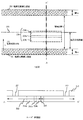
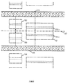
一つの活性層204を挟んで二つの触媒元素導入領域201、202を配置して結晶化を行い、触媒元素導入領域201からの結晶成長と、触媒元素導入領域202からの結晶成長とがぶつかる境界部205をソース領域またはドレイン領域となる領域204bに形成する。
【選択図】図2
Description
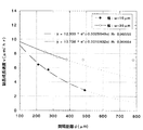
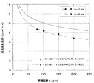
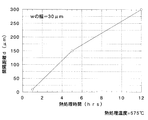
例えば、上記熱処理温度570℃に代えて580℃とした時、結晶成長速度vは9.5μm/hrであるため、4.4時間での結晶化が可能となる。
に示した。
また、結晶化後、ニッケルをリンのゲッタリング作用により除去又は低減しており、活性層811〜814中に残存する触媒元素の濃度は、1×10¹⁷atms/cm3以下、好ましくは1×1016atms/cm3である。(図8(E))
また、30nm厚の珪素を含む絶縁膜に対して50nm厚の熱酸化膜が加わるので、最終的なゲート絶縁膜815の膜厚は105nmとなる。
と定義する。(図10(A))
の方向に移動し、リンドープ領域に含まれるリンによってゲッタリングされて捕獲された。こうしてゲッタリング領域(リンドープ領域に対応する領域)が形成される。これにより、リンドープ領域に含まれるニッケルの濃度は2×10¹⁷atoms/cm3以下(好ましくは1×1016atoms/cm3以下)にまで低減される。
によってスピン密度の差となって現れる。現状では本実施例の作製工程に従って作製された結晶質シリコン膜のスピン密度は少なくとも 5×10¹⁷spins/cm3以下(好ましくは 3×10¹⁷spins/cm3以下)であることが判明している。ただし、この測定値は現存する測定装置の検出限界に近いので、実際のスピン密度はさらに低いと予想される。
本実施例の活性層を用いたTFTは、MOSFETに匹敵する電気特性を示した。本出願人が試作したTFT(但し、活性層の膜厚は30nm、ゲート絶縁膜の膜厚は100nm)からは次に示す様なデータが得られている。
(2)TFTの動作速度の指標となる電界効果移動度(μFE)が、Nチャネル型TFTで 200〜650cm2/Vs (代表的には 300〜500cm2/Vs )、Pチャネル型TFTで100〜300cm2/Vs(代表的には 150〜200cm2/Vs)と大きい。
(3)TFTの駆動電圧の指標となるしきい値電圧(Vth)が、Nチャネル型TFTで-0.5〜1.5 V、Pチャネル型TFTで-1.5〜0.5 Vと小さい。
従って、構造の説明はpチャネル型TFT1101の説明を参照すれば良い。なお、本実施例ではシングルゲート構造としているが、ダブルゲート構造もしくはトリプルゲート構造であっても良い。
これらの有機EL材料や無機材料は公知の材料を用いることができる。
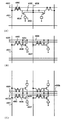
、(B)に示す。なお、本実施例において、4701はスイッチング用TFT4702のソース配線、4703はスイッチング用TFT4702のゲート配線、4704は電流制御用TFT、4705はコンデンサ(省略することも可能)、4706は電流供給線、、4707は電源制御用TFT、4709は電源制御用ゲート配線、4708はEL素子とする。電源制御用TFT4707の動作については特願平11−341272号を参照すると良い。
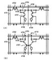
、(B)に示す。なお、本実施例において、4801はスイッチング用TFT4802のソース配線、4803はスイッチング用TFT4802のゲート配線、4804は電流制御用TFT、4805はコンデンサ(省略することも可能)、4806は電流供給線、、4807は消去用TFT、4808は消去用ゲート配線、4809はEL素子とする。消去用TFT4807の動作については特願平11−338786号を参照すると良い。
Claims (3)
- 第1の基板と、第2の基板と、前記第1の基板と前記第2の基板との間に設けられた液晶と、を有する半導体装置であって、
前記第1の基板は、
ソース領域、ドレイン領域及びチャネル形成領域を有する半導体膜を活性層とするTFTと、
前記TFT上に設けられた、開口部を有する層間絶縁膜と、
前記層間絶縁膜上に設けられ、前記開口部を介して前記ソース領域又は前記ドレイン領域と電気的に接続された画素電極と、を有し、
前記半導体膜は、結晶化を助長する触媒元素が導入された複数の領域から結晶成長された結晶構造を含む半導体膜からなり、
前記結晶構造を含む半導体膜は、前記結晶成長された領域同士がぶつかる領域に形成された境界部を有し、
前記境界部は、前記ソース領域又は前記ドレイン領域に含まれており、
前記第2の基板は対向電極を有し、
前記第1の基板と前記第2の基板とは、前記開口部と重なるように前記画素電極上に設けられたスペーサを介して貼り合わされていることを特徴とする半導体装置。 - 第1の基板と、第2の基板と、前記第1の基板と前記第2の基板との間に設けられた液晶と、を有する半導体装置であって、
前記第1の基板は、
ソース領域、ドレイン領域及び複数のチャネル形成領域を有する半導体膜を活性層とするTFTと、
前記TFT上に設けられた、開口部を有する層間絶縁膜と、
前記層間絶縁膜上に設けられ、前記開口部を介して前記ソース領域又は前記ドレイン領域と電気的に接続された画素電極と、を有し、
前記半導体膜は、結晶化を助長する触媒元素が導入された複数の領域から結晶成長された結晶構造を含む半導体膜からなり、
前記結晶構造を含む半導体膜は、前記結晶成長された領域同士がぶつかる領域に形成された境界部を有し、
前記境界部は、前記複数のチャネル形成領域の間に設けられ、
前記第2の基板は対向電極を有し、
前記第1の基板と前記第2の基板とは、前記開口部と重なるように前記画素電極上に設けられたスペーサを介して貼り合わされていることを特徴とする半導体装置。 - 請求項1又は2において、
前記結晶化を助長する触媒元素は、Ni、Fe、Co、Cu、Ge、Pdから選ばれた一種または複数種類の元素であることを特徴とする半導体装置。
Priority Applications (1)
| Application Number | Priority Date | Filing Date | Title |
|---|---|---|---|
| JP2011280822A JP2012104844A (ja) | 1999-05-14 | 2011-12-22 | 半導体装置 |
Applications Claiming Priority (3)
| Application Number | Priority Date | Filing Date | Title |
|---|---|---|---|
| JP13506299 | 1999-05-14 | ||
| JP1999135062 | 1999-05-14 | ||
| JP2011280822A JP2012104844A (ja) | 1999-05-14 | 2011-12-22 | 半導体装置 |
Related Parent Applications (1)
| Application Number | Title | Priority Date | Filing Date |
|---|---|---|---|
| JP2000138476A Division JP4912521B2 (ja) | 1999-05-14 | 2000-05-11 | 半導体装置の作製方法 |
Related Child Applications (1)
| Application Number | Title | Priority Date | Filing Date |
|---|---|---|---|
| JP2014147535A Division JP2014239241A (ja) | 1999-05-14 | 2014-07-18 | 半導体装置の作製方法 |
Publications (1)
| Publication Number | Publication Date |
|---|---|
| JP2012104844A true JP2012104844A (ja) | 2012-05-31 |
Family
ID=15143003
Family Applications (7)
| Application Number | Title | Priority Date | Filing Date |
|---|---|---|---|
| JP2000138476A Expired - Fee Related JP4912521B2 (ja) | 1999-05-14 | 2000-05-11 | 半導体装置の作製方法 |
| JP2011280822A Withdrawn JP2012104844A (ja) | 1999-05-14 | 2011-12-22 | 半導体装置 |
| JP2014147535A Withdrawn JP2014239241A (ja) | 1999-05-14 | 2014-07-18 | 半導体装置の作製方法 |
| JP2015129484A Expired - Lifetime JP6062497B2 (ja) | 1999-05-14 | 2015-06-29 | 液晶表示装置 |
| JP2016135882A Withdrawn JP2016208043A (ja) | 1999-05-14 | 2016-07-08 | 液晶表示装置 |
| JP2018121083A Withdrawn JP2018160693A (ja) | 1999-05-14 | 2018-06-26 | 半導体装置 |
| JP2019125729A Withdrawn JP2019204959A (ja) | 1999-05-14 | 2019-07-05 | 半導体装置 |
Family Applications Before (1)
| Application Number | Title | Priority Date | Filing Date |
|---|---|---|---|
| JP2000138476A Expired - Fee Related JP4912521B2 (ja) | 1999-05-14 | 2000-05-11 | 半導体装置の作製方法 |
Family Applications After (5)
| Application Number | Title | Priority Date | Filing Date |
|---|---|---|---|
| JP2014147535A Withdrawn JP2014239241A (ja) | 1999-05-14 | 2014-07-18 | 半導体装置の作製方法 |
| JP2015129484A Expired - Lifetime JP6062497B2 (ja) | 1999-05-14 | 2015-06-29 | 液晶表示装置 |
| JP2016135882A Withdrawn JP2016208043A (ja) | 1999-05-14 | 2016-07-08 | 液晶表示装置 |
| JP2018121083A Withdrawn JP2018160693A (ja) | 1999-05-14 | 2018-06-26 | 半導体装置 |
| JP2019125729A Withdrawn JP2019204959A (ja) | 1999-05-14 | 2019-07-05 | 半導体装置 |
Country Status (3)
| Country | Link |
|---|---|
| US (5) | US6680487B1 (ja) |
| EP (3) | EP2264764A2 (ja) |
| JP (7) | JP4912521B2 (ja) |
Families Citing this family (34)
| Publication number | Priority date | Publication date | Assignee | Title |
|---|---|---|---|---|
| JP4298131B2 (ja) * | 1999-05-14 | 2009-07-15 | 株式会社半導体エネルギー研究所 | 液晶表示装置の作製方法 |
| TW459275B (en) * | 1999-07-06 | 2001-10-11 | Semiconductor Energy Lab | Semiconductor device and method of fabricating the same |
| US7002659B1 (en) | 1999-11-30 | 2006-02-21 | Semiconductor Energy Laboratory Co., Ltd. | Liquid crystal panel and liquid crystal projector |
| KR100477103B1 (ko) | 2001-12-19 | 2005-03-18 | 삼성에스디아이 주식회사 | 금속유도화 측면결정화방법을 이용한 멀티플 게이트 박막트랜지스터 및 그의 제조방법 |
| KR100477102B1 (ko) | 2001-12-19 | 2005-03-17 | 삼성에스디아이 주식회사 | 금속유도화 측면결정화방법을 이용한 멀티플 게이트씨모스 박막 트랜지스터 및 그의 제조방법 |
| KR100426031B1 (ko) * | 2001-12-29 | 2004-04-03 | 엘지.필립스 엘시디 주식회사 | 능동행렬 유기전기발광소자 및 그의 제조 방법 |
| JP4190798B2 (ja) * | 2002-05-08 | 2008-12-03 | Nec液晶テクノロジー株式会社 | 薄膜トランジスタ及びその製造方法 |
| JP4338948B2 (ja) * | 2002-08-01 | 2009-10-07 | 株式会社半導体エネルギー研究所 | カーボンナノチューブ半導体素子の作製方法 |
| US8350466B2 (en) | 2004-09-17 | 2013-01-08 | Semiconductor Energy Laboratory Co., Ltd. | Display device and manufacturing method thereof |
| US7753751B2 (en) | 2004-09-29 | 2010-07-13 | Semiconductor Energy Laboratory Co., Ltd. | Method of fabricating the display device |
| US8772783B2 (en) * | 2004-10-14 | 2014-07-08 | Semiconductor Energy Laboratory Co., Ltd. | Display device |
| US8138502B2 (en) | 2005-08-05 | 2012-03-20 | Semiconductor Energy Laboratory Co., Ltd. | Light-emitting device and manufacturing method thereof |
| US8106865B2 (en) | 2006-06-02 | 2012-01-31 | Semiconductor Energy Laboratory Co., Ltd. | Display device and driving method thereof |
| JP2007329267A (ja) * | 2006-06-07 | 2007-12-20 | Toshiba Corp | 荷電粒子線描画装置及び荷電粒子線描画方法 |
| IL176673A0 (en) * | 2006-07-03 | 2007-07-04 | Fermon Israel | A variably displayable mobile device keyboard |
| DE602008006537D1 (de) * | 2007-03-02 | 2011-06-09 | Spinealign Medical Inc | Fraktur-fixationssystem |
| KR100875432B1 (ko) | 2007-05-31 | 2008-12-22 | 삼성모바일디스플레이주식회사 | 다결정 실리콘층의 제조 방법, 이를 이용하여 형성된박막트랜지스터, 그의 제조방법 및 이를 포함하는유기전계발광표시장치 |
| US8013633B2 (en) * | 2007-06-20 | 2011-09-06 | Hewlett-Packard Development Company, L.P. | Thin film transistor logic |
| KR100889626B1 (ko) | 2007-08-22 | 2009-03-20 | 삼성모바일디스플레이주식회사 | 박막트랜지스터, 그의 제조방법, 이를 구비한유기전계발광표시장치, 및 그의 제조방법 |
| KR100889627B1 (ko) | 2007-08-23 | 2009-03-20 | 삼성모바일디스플레이주식회사 | 박막트랜지스터, 그의 제조방법, 및 이를 구비한유기전계발광표시장치 |
| KR20100132020A (ko) * | 2008-02-29 | 2010-12-16 | 더 트러스티이스 오브 콜롬비아 유니버시티 인 더 시티 오브 뉴욕 | 균일한 결정질 si 막들을 제조하는 리소그래피 방법 |
| KR100982310B1 (ko) | 2008-03-27 | 2010-09-15 | 삼성모바일디스플레이주식회사 | 박막트랜지스터, 그의 제조방법, 및 이를 포함하는유기전계발광표시장치 |
| KR100989136B1 (ko) | 2008-04-11 | 2010-10-20 | 삼성모바일디스플레이주식회사 | 박막트랜지스터, 그의 제조방법, 및 이를 포함하는유기전계발광표시장치 |
| KR101002666B1 (ko) | 2008-07-14 | 2010-12-21 | 삼성모바일디스플레이주식회사 | 박막트랜지스터, 그의 제조방법, 및 이를 포함하는유기전계발광표시장치 |
| US8610155B2 (en) | 2008-11-18 | 2013-12-17 | Semiconductor Energy Laboratory Co., Ltd. | Light-emitting device, method for manufacturing the same, and cellular phone |
| TWI607670B (zh) | 2009-01-08 | 2017-12-01 | 半導體能源研究所股份有限公司 | 發光裝置及電子裝置 |
| US8471973B2 (en) * | 2009-06-12 | 2013-06-25 | Au Optronics Corporation | Pixel designs of improving the aperture ratio in an LCD |
| US8576209B2 (en) | 2009-07-07 | 2013-11-05 | Semiconductor Energy Laboratory Co., Ltd. | Display device |
| KR20130089044A (ko) * | 2012-02-01 | 2013-08-09 | 삼성디스플레이 주식회사 | 반도체 장치 및 그를 구비하는 평판표시장치 |
| TWI477874B (zh) * | 2012-03-28 | 2015-03-21 | E Ink Holdings Inc | 顯示裝置及其製作方法 |
| US9726940B2 (en) * | 2013-12-26 | 2017-08-08 | Sharp Kabushiki Kaisha | Active matrix substrate manufacturing method, display apparatus manufacturing method, and display apparatus |
| TWI577840B (zh) * | 2014-04-29 | 2017-04-11 | 中美矽晶製品股份有限公司 | 多晶矽鑄錠與來自其的矽晶圓 |
| CN106688115B (zh) | 2014-09-12 | 2019-06-14 | 世迈克琉明有限公司 | 半导体发光元件的制造方法 |
| CN117739838A (zh) * | 2023-09-28 | 2024-03-22 | 上海新昇半导体科技有限公司 | 一种直拉单晶硅直径测量方法、装置和直拉单晶硅生长装置 |
Citations (4)
| Publication number | Priority date | Publication date | Assignee | Title |
|---|---|---|---|---|
| JPH04286335A (ja) * | 1991-03-15 | 1992-10-12 | Seiko Epson Corp | 薄膜半導体装置の製造方法 |
| JPH06296020A (ja) * | 1993-02-15 | 1994-10-21 | Semiconductor Energy Lab Co Ltd | 半導体装置およびその製造方法 |
| JPH1062789A (ja) * | 1996-08-23 | 1998-03-06 | Sharp Corp | 液晶表示装置及びその製造方法 |
| JPH10209465A (ja) * | 1997-01-20 | 1998-08-07 | Semiconductor Energy Lab Co Ltd | 半導体装置およびその作製方法 |
Family Cites Families (128)
| Publication number | Priority date | Publication date | Assignee | Title |
|---|---|---|---|---|
| US3404198A (en) | 1965-07-30 | 1968-10-01 | Ashland Oil Inc | Phenol-formaldehyde-urea resin and method of preparation |
| JPS59222817A (ja) * | 1983-06-02 | 1984-12-14 | Asahi Glass Co Ltd | 液晶表示装置 |
| JPS61184518A (ja) | 1985-02-12 | 1986-08-18 | Semiconductor Energy Lab Co Ltd | 液晶表示装置作成方法 |
| US4775225A (en) * | 1985-05-16 | 1988-10-04 | Canon Kabushiki Kaisha | Liquid crystal device having pillar spacers with small base periphery width in direction perpendicular to orientation treatment |
| US5963288A (en) * | 1987-08-20 | 1999-10-05 | Semiconductor Energy Laboratory Co., Ltd. | Liquid crystal device having sealant and spacers made from the same material |
| JPS6350817A (ja) * | 1986-08-20 | 1988-03-03 | Semiconductor Energy Lab Co Ltd | 液晶電気光学装置作製方法 |
| US5379139A (en) * | 1986-08-20 | 1995-01-03 | Semiconductor Energy Laboratory Co., Ltd. | Liquid crystal device and method for manufacturing same with spacers formed by photolithography |
| US5327001A (en) * | 1987-09-09 | 1994-07-05 | Casio Computer Co., Ltd. | Thin film transistor array having single light shield layer over transistors and gate and drain lines |
| DE3732519A1 (de) * | 1987-09-26 | 1989-04-06 | Olympia Aeg | Anordnung zum eingeben und verarbeiten von zeichen und/oder grafischen mustern |
| JP2742057B2 (ja) | 1988-07-14 | 1998-04-22 | シャープ株式会社 | 薄膜elパネル |
| JP2720473B2 (ja) * | 1988-09-21 | 1998-03-04 | セイコーエプソン株式会社 | 薄膜トランジスタ及びその製造方法 |
| US5189405A (en) | 1989-01-26 | 1993-02-23 | Sharp Kabushiki Kaisha | Thin film electroluminescent panel |
| JPH0329291A (ja) | 1989-06-27 | 1991-02-07 | Sumitomo Bakelite Co Ltd | 有機分散型elランプ用捕水フィルム |
| US5062198A (en) * | 1990-05-08 | 1991-11-05 | Keytec, Inc. | Method of making a transparent touch screen switch assembly |
| JPH04133036A (ja) * | 1990-09-25 | 1992-05-07 | Seiko Instr Inc | 光弁基板用単結晶薄膜半導体装置 |
| JP2794678B2 (ja) * | 1991-08-26 | 1998-09-10 | 株式会社 半導体エネルギー研究所 | 絶縁ゲイト型半導体装置およびその作製方法 |
| CA2082136C (en) * | 1991-11-08 | 1998-01-06 | Hiroshi Tsujioka | Coordinates input device |
| US5739882A (en) * | 1991-11-18 | 1998-04-14 | Semiconductor Energy Laboratory Co., Ltd. | LCD polymerized column spacer formed on a modified substrate, from an acrylic resin, on a surface having hydrophilic and hydrophobic portions, or at regular spacings |
| JPH05281558A (ja) | 1992-04-03 | 1993-10-29 | Toshiba Corp | 液晶表示素子 |
| JPH05289109A (ja) * | 1992-04-08 | 1993-11-05 | Sony Corp | 液晶表示装置 |
| JP3251690B2 (ja) | 1992-06-01 | 2002-01-28 | 株式会社東芝 | 液晶表示素子 |
| EP0603420B1 (en) * | 1992-07-15 | 2001-06-13 | Kabushiki Kaisha Toshiba | Liquid crystal display |
| JPH0659228A (ja) | 1992-08-12 | 1994-03-04 | Toshiba Corp | 液晶表示素子の製造方法 |
| JP2924506B2 (ja) * | 1992-10-27 | 1999-07-26 | 日本電気株式会社 | アクティブマトリックス型液晶表示装置の画素構造 |
| JP3497198B2 (ja) | 1993-02-03 | 2004-02-16 | 株式会社半導体エネルギー研究所 | 半導体装置および薄膜トランジスタの作製方法 |
| US5843225A (en) | 1993-02-03 | 1998-12-01 | Semiconductor Energy Laboratory Co., Ltd. | Process for fabricating semiconductor and process for fabricating semiconductor device |
| EP0612102B1 (en) | 1993-02-15 | 2001-09-26 | Semiconductor Energy Laboratory Co., Ltd. | Process for the fabrication of a crystallised semiconductor layer |
| JP3562588B2 (ja) * | 1993-02-15 | 2004-09-08 | 株式会社半導体エネルギー研究所 | 半導体装置の製造方法 |
| US6997985B1 (en) * | 1993-02-15 | 2006-02-14 | Semiconductor Energy Laboratory Co., Ltd. | Semiconductor, semiconductor device, and method for fabricating the same |
| JP3210126B2 (ja) | 1993-03-15 | 2001-09-17 | 株式会社東芝 | 液晶表示装置の製造方法 |
| US5539545A (en) * | 1993-05-18 | 1996-07-23 | Semiconductor Energy Laboratory Co., Ltd. | Method of making LCD in which resin columns are cured and the liquid crystal is reoriented |
| JPH06332011A (ja) * | 1993-05-18 | 1994-12-02 | Sony Corp | 半導体集合基板及び半導体装置 |
| US5481121A (en) | 1993-05-26 | 1996-01-02 | Semiconductor Energy Laboratory Co., Ltd. | Semiconductor device having improved crystal orientation |
| KR100186886B1 (ko) * | 1993-05-26 | 1999-04-15 | 야마자끼 승페이 | 반도체장치 제작방법 |
| JP2791858B2 (ja) | 1993-06-25 | 1998-08-27 | 株式会社半導体エネルギー研究所 | 半導体装置作製方法 |
| US5594569A (en) | 1993-07-22 | 1997-01-14 | Semiconductor Energy Laboratory Co., Ltd. | Liquid-crystal electro-optical apparatus and method of manufacturing the same |
| JP2762215B2 (ja) | 1993-08-12 | 1998-06-04 | 株式会社半導体エネルギー研究所 | 薄膜トランジスタおよび半導体装置の作製方法 |
| JPH07335904A (ja) * | 1994-06-14 | 1995-12-22 | Semiconductor Energy Lab Co Ltd | 薄膜半導体集積回路 |
| JP3431033B2 (ja) | 1993-10-29 | 2003-07-28 | 株式会社半導体エネルギー研究所 | 半導体作製方法 |
| US5923962A (en) | 1993-10-29 | 1999-07-13 | Semiconductor Energy Laboratory Co., Ltd. | Method for manufacturing a semiconductor device |
| TW264575B (ja) | 1993-10-29 | 1995-12-01 | Handotai Energy Kenkyusho Kk | |
| TW272319B (ja) | 1993-12-20 | 1996-03-11 | Sharp Kk | |
| JP3269734B2 (ja) | 1994-06-21 | 2002-04-02 | シャープ株式会社 | 半導体装置及びその製造方法 |
| JP3109967B2 (ja) * | 1993-12-28 | 2000-11-20 | キヤノン株式会社 | アクティブマトリクス基板の製造方法 |
| JP3378078B2 (ja) | 1994-02-23 | 2003-02-17 | 株式会社半導体エネルギー研究所 | 半導体装置の作製方法 |
| US6162667A (en) * | 1994-03-28 | 2000-12-19 | Sharp Kabushiki Kaisha | Method for fabricating thin film transistors |
| JP2547523B2 (ja) * | 1994-04-04 | 1996-10-23 | インターナショナル・ビジネス・マシーンズ・コーポレイション | 液晶表示装置及びその製造方法 |
| JP3192546B2 (ja) | 1994-04-15 | 2001-07-30 | シャープ株式会社 | 半導体装置およびその製造方法 |
| JP3067949B2 (ja) | 1994-06-15 | 2000-07-24 | シャープ株式会社 | 電子装置および液晶表示装置 |
| DE69529493T2 (de) * | 1994-06-20 | 2003-10-30 | Canon K.K., Tokio/Tokyo | Anzeigevorrichtung und Verfahren zu ihrer Herstellung |
| JP3894969B2 (ja) | 1994-09-30 | 2007-03-22 | 株式会社半導体エネルギー研究所 | 半導体装置の作製方法 |
| US5915174A (en) | 1994-09-30 | 1999-06-22 | Semiconductor Energy Laboratory Co., Ltd. | Semiconductor device and method for producing the same |
| JP3277082B2 (ja) * | 1994-11-22 | 2002-04-22 | シャープ株式会社 | 半導体装置およびその製造方法 |
| JPH08248427A (ja) | 1995-03-13 | 1996-09-27 | Semiconductor Energy Lab Co Ltd | 液晶表示装置 |
| JPH08297286A (ja) * | 1995-04-26 | 1996-11-12 | Internatl Business Mach Corp <Ibm> | 液晶表示装置 |
| US5771562A (en) | 1995-05-02 | 1998-06-30 | Motorola, Inc. | Passivation of organic devices |
| JPH0926603A (ja) * | 1995-05-08 | 1997-01-28 | Semiconductor Energy Lab Co Ltd | 表示装置 |
| JPH0973093A (ja) | 1995-09-06 | 1997-03-18 | Toshiba Electron Eng Corp | 液晶表示装置、及びその製造方法 |
| TW373098B (en) * | 1995-09-06 | 1999-11-01 | Toshiba Corp | Liquid crystal exposure component and its fabricating method |
| TW439003B (en) | 1995-11-17 | 2001-06-07 | Semiconductor Energy Lab | Display device |
| US5686360A (en) | 1995-11-30 | 1997-11-11 | Motorola | Passivation of organic devices |
| US5811177A (en) | 1995-11-30 | 1998-09-22 | Motorola, Inc. | Passivation of electroluminescent organic devices |
| JP3124480B2 (ja) | 1995-12-12 | 2001-01-15 | 株式会社半導体エネルギー研究所 | 半導体装置の作製方法 |
| TW309633B (ja) | 1995-12-14 | 1997-07-01 | Handotai Energy Kenkyusho Kk | |
| JP3310152B2 (ja) | 1996-01-18 | 2002-07-29 | 株式会社東芝 | 液晶表示装置およびその製造方法 |
| JP3647542B2 (ja) * | 1996-02-20 | 2005-05-11 | 株式会社半導体エネルギー研究所 | 液晶表示装置 |
| US6236445B1 (en) * | 1996-02-22 | 2001-05-22 | Hughes Electronics Corporation | Method for making topographic projections |
| JPH1054999A (ja) * | 1996-06-04 | 1998-02-24 | Canon Inc | 表示装置とその製造法 |
| JP3871736B2 (ja) * | 1996-06-25 | 2007-01-24 | 株式会社半導体エネルギー研究所 | 液晶表示装置及び撮影装置及び情報処理装置 |
| US5986729A (en) * | 1996-07-10 | 1999-11-16 | Matsushita Electric Industrial Co., Ltd. | Liquid crystal display device and method of manufacturing the same |
| US5693956A (en) | 1996-07-29 | 1997-12-02 | Motorola | Inverted oleds on hard plastic substrate |
| JPH1048667A (ja) * | 1996-08-01 | 1998-02-20 | Seiko Epson Corp | 液晶パネル用基板およびその製造方法並びに投射型表示装置 |
| JPH1068955A (ja) | 1996-08-29 | 1998-03-10 | Toshiba Corp | 液晶表示素子 |
| JPH1091099A (ja) * | 1996-09-18 | 1998-04-10 | Toshiba Corp | 液晶表示装置 |
| JPH1096955A (ja) | 1996-09-24 | 1998-04-14 | Toshiba Corp | 液晶表示装置 |
| US5973763A (en) * | 1996-10-16 | 1999-10-26 | Seiko Epson Corporation | Liquid crystal device including supporting columns |
| JP3525316B2 (ja) * | 1996-11-12 | 2004-05-10 | 株式会社半導体エネルギー研究所 | アクティブマトリクス型表示装置 |
| JP3792324B2 (ja) * | 1996-12-06 | 2006-07-05 | セイコーエプソン株式会社 | 液晶パネル用基板およびその製造方法並びに液晶パネルおよび投写型表示装置 |
| JPH11133463A (ja) | 1997-10-31 | 1999-05-21 | Semiconductor Energy Lab Co Ltd | アクティブマトリクス型液晶表示装置及び電子機器 |
| US6088070A (en) | 1997-01-17 | 2000-07-11 | Semiconductor Energy Laboratory Co., Ltd. | Active matrix liquid crystal with capacitor between light blocking film and pixel connecting electrode |
| TW386238B (en) | 1997-01-20 | 2000-04-01 | Semiconductor Energy Lab | Semiconductor device and method of manufacturing the same |
| JP3980117B2 (ja) * | 1997-04-26 | 2007-09-26 | 株式会社半導体エネルギー研究所 | 半導体装置の作製方法 |
| US5831710A (en) * | 1997-02-06 | 1998-11-03 | International Business Machines Corporation | Liquid crystal display |
| JPH10228022A (ja) | 1997-02-17 | 1998-08-25 | Semiconductor Energy Lab Co Ltd | 液晶表示装置およびその作製方法 |
| JP3782194B2 (ja) * | 1997-02-28 | 2006-06-07 | 株式会社東芝 | アクティブマトリクス型液晶表示装置 |
| TW379360B (en) | 1997-03-03 | 2000-01-11 | Semiconductor Energy Lab | Method of manufacturing a semiconductor device |
| JP3032801B2 (ja) | 1997-03-03 | 2000-04-17 | 株式会社半導体エネルギー研究所 | 半導体装置の作製方法 |
| US5952778A (en) | 1997-03-18 | 1999-09-14 | International Business Machines Corporation | Encapsulated organic light emitting device |
| JPH10268316A (ja) | 1997-03-24 | 1998-10-09 | Toshiba Corp | 液晶表示素子の製造方法 |
| JP3871764B2 (ja) * | 1997-03-26 | 2007-01-24 | 株式会社半導体エネルギー研究所 | 反射型の表示装置 |
| JPH10268361A (ja) | 1997-03-27 | 1998-10-09 | Semiconductor Energy Lab Co Ltd | 液晶表示装置およびその製造方法 |
| US5978063A (en) * | 1997-04-15 | 1999-11-02 | Xerox Corporation | Smart spacers for active matrix liquid crystal projection light valves |
| JP3290375B2 (ja) | 1997-05-12 | 2002-06-10 | 松下電器産業株式会社 | 有機電界発光素子 |
| JP3998755B2 (ja) | 1997-05-22 | 2007-10-31 | 株式会社半導体エネルギー研究所 | 半導体表示装置 |
| JPH10339889A (ja) | 1997-06-09 | 1998-12-22 | Semiconductor Energy Lab Co Ltd | 電気光学装置およびその製造方法 |
| JPH10325959A (ja) | 1997-05-26 | 1998-12-08 | Semiconductor Energy Lab Co Ltd | 表示装置 |
| US6465268B2 (en) * | 1997-05-22 | 2002-10-15 | Semiconductor Energy Laboratory Co., Ltd. | Method of manufacturing an electro-optical device |
| US6198220B1 (en) | 1997-07-11 | 2001-03-06 | Emagin Corporation | Sealing structure for organic light emitting devices |
| JPH1184386A (ja) | 1997-09-01 | 1999-03-26 | Toshiba Corp | アクティブマトリクス型液晶表示装置 |
| US6717356B1 (en) | 1997-09-18 | 2004-04-06 | Lg Electronics Inc. | Organic electroluminescent device with trapezoidal walls |
| JP3919900B2 (ja) * | 1997-09-19 | 2007-05-30 | 株式会社半導体エネルギー研究所 | 液晶表示装置およびその作製方法 |
| JP4159633B2 (ja) | 1997-09-19 | 2008-10-01 | 株式会社半導体エネルギー研究所 | 半導体装置およびその作製方法並びに電子機器 |
| JPH1195194A (ja) | 1997-09-24 | 1999-04-09 | Toshiba Electronic Engineering Corp | 液晶表示素子およびその製造方法 |
| JP3489409B2 (ja) * | 1997-09-26 | 2004-01-19 | セイコーエプソン株式会社 | 液晶表示パネルの製造方法及び液晶表示パネル |
| JP3699828B2 (ja) * | 1997-10-06 | 2005-09-28 | シャープ株式会社 | 液晶表示素子およびその製造方法 |
| KR100249784B1 (ko) | 1997-11-20 | 2000-04-01 | 정선종 | 고분자복합막을이용한유기물혹은고분자전기발광소자의패키징방법 |
| JPH11295746A (ja) * | 1998-02-16 | 1999-10-29 | Sharp Corp | 液晶素子の製造方法、液晶注入装置および液晶注入システム |
| JP4011725B2 (ja) * | 1998-04-24 | 2007-11-21 | 東芝松下ディスプレイテクノロジー株式会社 | 液晶表示装置 |
| JPH11341272A (ja) | 1998-05-22 | 1999-12-10 | Noritsu Koki Co Ltd | 画像処理装置及び画像処理方法 |
| JPH11338786A (ja) | 1998-05-29 | 1999-12-10 | Pfu Ltd | 主記憶アドレスバス診断方法およびその診断装置並びに記録媒体 |
| KR100282393B1 (ko) | 1998-06-17 | 2001-02-15 | 구자홍 | 유기이엘(el)디스플레이소자제조방법 |
| US6146225A (en) | 1998-07-30 | 2000-11-14 | Agilent Technologies, Inc. | Transparent, flexible permeability barrier for organic electroluminescent devices |
| JP3104687B2 (ja) * | 1998-08-28 | 2000-10-30 | 日本電気株式会社 | 液晶表示装置 |
| KR100324914B1 (ko) * | 1998-09-25 | 2002-02-28 | 니시무로 타이죠 | 기판의 검사방법 |
| JP3661443B2 (ja) * | 1998-10-27 | 2005-06-15 | 株式会社日立製作所 | アクティブマトリクス液晶表示装置 |
| US6274887B1 (en) | 1998-11-02 | 2001-08-14 | Semiconductor Energy Laboratory Co., Ltd. | Semiconductor device and manufacturing method therefor |
| KR100327696B1 (ko) * | 1998-11-16 | 2002-03-09 | 니시무로 타이죠 | 액정표시장치 및 착색층 부재 |
| US6465115B2 (en) | 1998-12-09 | 2002-10-15 | Eastman Kodak Company | Electroluminescent device with anthracene derivatives hole transport layer |
| US6285247B1 (en) * | 1999-01-21 | 2001-09-04 | Agere Systems Guardian Corporation | Optimized low voltage CMOS operation |
| JP4372943B2 (ja) * | 1999-02-23 | 2009-11-25 | 株式会社半導体エネルギー研究所 | 半導体装置およびその作製方法 |
| US7821065B2 (en) * | 1999-03-02 | 2010-10-26 | Semiconductor Energy Laboratory Co., Ltd. | Semiconductor device comprising a thin film transistor comprising a semiconductor thin film and method of manufacturing the same |
| US6531993B1 (en) * | 1999-03-05 | 2003-03-11 | Semiconductor Energy Laboratory Co., Ltd. | Active matrix type display device |
| JP4298131B2 (ja) * | 1999-05-14 | 2009-07-15 | 株式会社半導体エネルギー研究所 | 液晶表示装置の作製方法 |
| JP2001005007A (ja) * | 1999-06-18 | 2001-01-12 | Hitachi Ltd | 液晶表示装置 |
| TW459275B (en) * | 1999-07-06 | 2001-10-11 | Semiconductor Energy Lab | Semiconductor device and method of fabricating the same |
| JP3942770B2 (ja) | 1999-09-22 | 2007-07-11 | 株式会社半導体エネルギー研究所 | El表示装置及び電子装置 |
| US6413645B1 (en) | 2000-04-20 | 2002-07-02 | Battelle Memorial Institute | Ultrabarrier substrates |
| US6226890B1 (en) | 2000-04-07 | 2001-05-08 | Eastman Kodak Company | Desiccation of moisture-sensitive electronic devices |
-
2000
- 2000-05-08 US US09/567,403 patent/US6680487B1/en not_active Expired - Lifetime
- 2000-05-11 EP EP10178747A patent/EP2264764A2/en not_active Withdrawn
- 2000-05-11 EP EP09006485.8A patent/EP2105966B1/en not_active Expired - Lifetime
- 2000-05-11 EP EP00109971A patent/EP1052700A1/en not_active Ceased
- 2000-05-11 JP JP2000138476A patent/JP4912521B2/ja not_active Expired - Fee Related
-
2003
- 2003-03-14 US US10/387,436 patent/US6909115B2/en not_active Expired - Fee Related
-
2005
- 2005-06-14 US US11/151,202 patent/US7696514B2/en not_active Expired - Fee Related
-
2010
- 2010-04-07 US US12/755,801 patent/US8026518B2/en not_active Expired - Fee Related
-
2011
- 2011-09-15 US US13/233,120 patent/US8314426B2/en not_active Expired - Fee Related
- 2011-12-22 JP JP2011280822A patent/JP2012104844A/ja not_active Withdrawn
-
2014
- 2014-07-18 JP JP2014147535A patent/JP2014239241A/ja not_active Withdrawn
-
2015
- 2015-06-29 JP JP2015129484A patent/JP6062497B2/ja not_active Expired - Lifetime
-
2016
- 2016-07-08 JP JP2016135882A patent/JP2016208043A/ja not_active Withdrawn
-
2018
- 2018-06-26 JP JP2018121083A patent/JP2018160693A/ja not_active Withdrawn
-
2019
- 2019-07-05 JP JP2019125729A patent/JP2019204959A/ja not_active Withdrawn
Patent Citations (4)
| Publication number | Priority date | Publication date | Assignee | Title |
|---|---|---|---|---|
| JPH04286335A (ja) * | 1991-03-15 | 1992-10-12 | Seiko Epson Corp | 薄膜半導体装置の製造方法 |
| JPH06296020A (ja) * | 1993-02-15 | 1994-10-21 | Semiconductor Energy Lab Co Ltd | 半導体装置およびその製造方法 |
| JPH1062789A (ja) * | 1996-08-23 | 1998-03-06 | Sharp Corp | 液晶表示装置及びその製造方法 |
| JPH10209465A (ja) * | 1997-01-20 | 1998-08-07 | Semiconductor Energy Lab Co Ltd | 半導体装置およびその作製方法 |
Also Published As
| Publication number | Publication date |
|---|---|
| US8314426B2 (en) | 2012-11-20 |
| US20120062809A1 (en) | 2012-03-15 |
| US6909115B2 (en) | 2005-06-21 |
| EP1052700A1 (en) | 2000-11-15 |
| EP2105966A3 (en) | 2011-03-23 |
| JP6062497B2 (ja) | 2017-01-18 |
| JP4912521B2 (ja) | 2012-04-11 |
| EP2105966A2 (en) | 2009-09-30 |
| US20100195012A1 (en) | 2010-08-05 |
| US20030173567A1 (en) | 2003-09-18 |
| US20050269569A1 (en) | 2005-12-08 |
| JP2016208043A (ja) | 2016-12-08 |
| JP2019204959A (ja) | 2019-11-28 |
| US7696514B2 (en) | 2010-04-13 |
| JP2014239241A (ja) | 2014-12-18 |
| JP2001036094A (ja) | 2001-02-09 |
| EP2105966B1 (en) | 2017-08-23 |
| JP2015222429A (ja) | 2015-12-10 |
| US8026518B2 (en) | 2011-09-27 |
| EP2264764A2 (en) | 2010-12-22 |
| US6680487B1 (en) | 2004-01-20 |
| JP2018160693A (ja) | 2018-10-11 |
Similar Documents
| Publication | Publication Date | Title |
|---|---|---|
| JP4912521B2 (ja) | 半導体装置の作製方法 | |
| JP6170641B1 (ja) | 液晶表示装置 | |
| US20030062499A1 (en) | Electro-optical device and manufacturing method thereof | |
| JP4578609B2 (ja) | 電気光学装置 | |
| JP2015038612A (ja) | 液晶表示装置 | |
| JP4531194B2 (ja) | 電気光学装置及び電子機器 | |
| JP4651777B2 (ja) | 半導体装置の作製方法 | |
| JP4260334B2 (ja) | 半導体装置の作製方法 | |
| JP4850763B2 (ja) | 半導体装置の作製方法 | |
| JP4712156B2 (ja) | 半導体装置の作製方法 |
Legal Events
| Date | Code | Title | Description |
|---|---|---|---|
| A977 | Report on retrieval |
Free format text: JAPANESE INTERMEDIATE CODE: A971007 Effective date: 20130830 |
|
| A131 | Notification of reasons for refusal |
Free format text: JAPANESE INTERMEDIATE CODE: A131 Effective date: 20130924 |
|
| A521 | Request for written amendment filed |
Free format text: JAPANESE INTERMEDIATE CODE: A523 Effective date: 20131105 |
|
| A131 | Notification of reasons for refusal |
Free format text: JAPANESE INTERMEDIATE CODE: A131 Effective date: 20140107 |
|
| A521 | Request for written amendment filed |
Free format text: JAPANESE INTERMEDIATE CODE: A523 Effective date: 20140129 |
|
| A02 | Decision of refusal |
Free format text: JAPANESE INTERMEDIATE CODE: A02 Effective date: 20140430 |
|
| A521 | Request for written amendment filed |
Free format text: JAPANESE INTERMEDIATE CODE: A523 Effective date: 20140718 |
|
| A761 | Written withdrawal of application |
Free format text: JAPANESE INTERMEDIATE CODE: A761 Effective date: 20140722 |