EP0197639B1 - Halbleiterspeicheranordnung - Google Patents
Halbleiterspeicheranordnung Download PDFInfo
- Publication number
- EP0197639B1 EP0197639B1 EP86301209A EP86301209A EP0197639B1 EP 0197639 B1 EP0197639 B1 EP 0197639B1 EP 86301209 A EP86301209 A EP 86301209A EP 86301209 A EP86301209 A EP 86301209A EP 0197639 B1 EP0197639 B1 EP 0197639B1
- Authority
- EP
- European Patent Office
- Prior art keywords
- sense amplifier
- leads
- sbl1
- bit line
- pair
- Prior art date
- Legal status (The legal status is an assumption and is not a legal conclusion. Google has not performed a legal analysis and makes no representation as to the accuracy of the status listed.)
- Expired - Lifetime
Links
Images



Classifications
-
- H—ELECTRICITY
- H10—SEMICONDUCTOR DEVICES; ELECTRIC SOLID-STATE DEVICES NOT OTHERWISE PROVIDED FOR
- H10B—ELECTRONIC MEMORY DEVICES
- H10B12/00—Dynamic random access memory [DRAM] devices
- H10B12/30—DRAM devices comprising one-transistor - one-capacitor [1T-1C] memory cells
- H10B12/48—Data lines or contacts therefor
- H10B12/485—Bit line contacts
-
- H—ELECTRICITY
- H10—SEMICONDUCTOR DEVICES; ELECTRIC SOLID-STATE DEVICES NOT OTHERWISE PROVIDED FOR
- H10W—GENERIC PACKAGES, INTERCONNECTIONS, CONNECTORS OR OTHER CONSTRUCTIONAL DETAILS OF DEVICES COVERED BY CLASS H10
- H10W20/00—Interconnections in chips, wafers or substrates
- H10W20/40—Interconnections external to wafers or substrates, e.g. back-end-of-line [BEOL] metallisations or vias connecting to gate electrodes
- H10W20/495—Capacitive arrangements or effects of, or between wiring layers
-
- G—PHYSICS
- G11—INFORMATION STORAGE
- G11C—STATIC STORES
- G11C11/00—Digital stores characterised by the use of particular electric or magnetic storage elements; Storage elements therefor
- G11C11/21—Digital stores characterised by the use of particular electric or magnetic storage elements; Storage elements therefor using electric elements
- G11C11/34—Digital stores characterised by the use of particular electric or magnetic storage elements; Storage elements therefor using electric elements using semiconductor devices
- G11C11/40—Digital stores characterised by the use of particular electric or magnetic storage elements; Storage elements therefor using electric elements using semiconductor devices using transistors
- G11C11/401—Digital stores characterised by the use of particular electric or magnetic storage elements; Storage elements therefor using electric elements using semiconductor devices using transistors forming cells needing refreshing or charge regeneration, i.e. dynamic cells
- G11C11/4063—Auxiliary circuits, e.g. for addressing, decoding, driving, writing, sensing or timing
- G11C11/407—Auxiliary circuits, e.g. for addressing, decoding, driving, writing, sensing or timing for memory cells of the field-effect type
- G11C11/409—Read-write [R-W] circuits
- G11C11/4097—Bit-line organisation, e.g. bit-line layout, folded bit lines
-
- G—PHYSICS
- G11—INFORMATION STORAGE
- G11C—STATIC STORES
- G11C7/00—Arrangements for writing information into, or reading information out from, a digital store
- G11C7/06—Sense amplifiers; Associated circuits, e.g. timing or triggering circuits
- G11C7/065—Differential amplifiers of latching type
-
- G—PHYSICS
- G11—INFORMATION STORAGE
- G11C—STATIC STORES
- G11C7/00—Arrangements for writing information into, or reading information out from, a digital store
- G11C7/18—Bit line organisation; Bit line lay-out
-
- H—ELECTRICITY
- H10—SEMICONDUCTOR DEVICES; ELECTRIC SOLID-STATE DEVICES NOT OTHERWISE PROVIDED FOR
- H10B—ELECTRONIC MEMORY DEVICES
- H10B12/00—Dynamic random access memory [DRAM] devices
- H10B12/01—Manufacture or treatment
- H10B12/09—Manufacture or treatment with simultaneous manufacture of the peripheral circuit region and memory cells
Definitions
- the present invention relates to a semiconductor memory device. More particularly, the present invention relates to a semiconductor memory device comprising a large-scale integrated circuit such as a dynamic random access memory (hereinafter referred to as a dynamic RAM).
- a dynamic RAM a dynamic random access memory
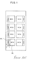
- Fig. 1 shows an arrangement of a conventional dynamic RAM
- Fig. 2 shows an arrangement of a sense amplifier portion included in a conventional dynamic RAM.
- a memory cell array MCA comprises word lines WL, bit lines BL and a sense amplifier array SAA. Although a plurality of word lines WL and bit lines BL are provided in a memory cell array MCA according to the memory capacity, only one word line and one bit line are shown in Fig. 1.
- a sense amplifier in the end portion of the sense amplifier array SAA surrounded by a, b, c and d in Fig. 1 will be described in the following.
- One end of each of the aluminum leads SBL1, SBL1 ,..., SBL3 in the sense amplifier is connected to the associated bit line and the aluminium lead 1 short-circuits a cell plate of a memory cell not shown.
- the sense amplifier comprises insulated field effect transistors (hereinafter referred to as FET's), the FET's including gates G1,... G6 respectively.
- FET's insulated field effect transistors
- a sense amplifier activation signal is applied to one end of the aluminium lead 2.
- SBL3 are connected respectively to the drains of the FET's and the aluminium lead 2 is connected to the sources of the FET's.
- the regions surrounded by dotted lines in Fig. 2 represent activation regions for forming the sources and drains of the FET's.
- the sense amplifiers are arrayed so that the distances d1, d2 and d3 between the aluminium leads of any adjacent pair of sense amplifiers are equal to the respective distances between the aluminium leads of each other corresponding pair of sense amplifiers in the sequential array, while the distances d 1a , d 2a and d 3a between the aluminium leads SBL1 and SBL1 of the outermost sense amplifier of the sense amplifier array SAA and the aluminium lead 1 provided further outside are different from the distances d1, d2 and d3.
- the distances d 1a , d 2a and d 3a are respectively smaller than d1, d2 and d3.
- Fig. 3 shows a state in which memory cells and sense amplifiers are connected.
- the bit line BL1 is connected with the drain of a FET QC1 forming a memory cell and the drain of a FET QD1 forming a dummy cell and further connected with the source of a FET QS1 forming a sense amplifier via the aluminum lead SBL1.
- the bit line BL1 is connected with the drain of a FET QC2 forming a memory cell and the drain of a FET QD2 forming a dummy cell and further connected with the source of a FET QS2 via the aluminum lead SBL1 .
- an activation signal S is supplied to the respective drains of the FET's QS1 and QS2.
- the gate of the FET QS1 is connected to the aluminum lead SBL1 and the gate of the FET QS2 is connected to the aluminum lead SBL1.
- the word line WL1 is connected with the gate of the FET QC1 and the source thereof is connected with a capacitor CC1 so that a memory cell is formed by the capacitor CC1 and the FET QC1.
- the word line WL2 is connected with the gate of the FET QC2 and the source of the FET QC2 is connected with a capacitor CC2 so that a memory cell is formed by the capacitor CC2 and the FET QC2.
- the dummy word line DWL1 is connected with the gate of the FET QD1 and the source thereof is connected with a capacitor CD1 so that a dummy cell is formed by the capacitor CD1 and the FET QD1.
- the dummy word line DWL2 is connected with the gate of the FET QD2 and the source thereof is connected with a capacitor CD2 so that a dummy cell is formed by the capacitor CD2 and the FET QD2.
- a FET QR1 for discharging the dummy cell is connected to a point of connection between the source of the FET QD1 and the capacitor CD1.
- the drain of a FET QR2 for discharging the dummy cell is connected to a point of connection between the FET QD2 and the capacitor CD2.
- a dummy cell reset signal RST is supplied to the respective gates of the FET's QR1 and QR2.
- the aluminum leads SBL1 and SBL1 may be connected electrically with floating capacities CS10 and CS20 for grounding potential and an interline capacity CS12 between the aluminum leads SBL1 and SBL1 . Furthermore, the aluminum lead SBL1 may be connected with an interline capacity CS11 for the outer aluminum lead 1 and the aluminum lead SBL1 may be connected with an interline capacity CS23 for the adjacent aluminum lead SBL2 .
- the aluminum leads in the sense amplifiers are disposed so that each capacity associated therewith is almost equal to the sum of a floating capacity and an interline capacity.
- the distance between the outermost aluminum lead SBL1 of the sense amplifier array SAA and the aluminum lead 1 existing further outside is smaller than the distance between other aluminum leads and accordingly, the capacity associated with the aluminum lead SBL 1 is larger than the capacity associated with other aluminum leads.
- a method may be considered in which the distance between an aluminum lead extending from the aluminum lead 1 to be disposed outside the bit line BL1 and the bit line BL1 is made equal to the distance between the bit line BL1 and the bit line BL2.
- the capacity connected to the bit line BL1 and the capacity connected to the bit line BL1 would be different in the end because the capacity associated with the aluminum lead SBL1 and the capacity associated with the aluminum lead SBL1 are different as described above and in the example shown in Fig. 2, the capacity associated with the bit line BL1 (hereinafter referred to as CBL1) is larger than the capacity associated with the bit line BL1 (hereinafter referred to as CBL1 ).
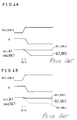
- Figs. 4A and 4B are waveform diagrams showing a part of operation of a conventional dynamic RAM. Referring to Figs. 4A and 4B, the operation of a dynamic RAM comprising bit lines, aluminum leads connected to the bit lines and an outer aluminum lead as described above will be described in the following, with regard to a case of reading the content stored in the capacitor CC1 of the memory cell shown in Fig. 3.
- the dummy cell reset signal RST rises to "H” and the FET's QR1 and QR2 are conducted so that the capacitors CD1 and CD2 are discharged.
- the bit lines BL1 and BL1 are precharged at the level "H” by precharge means not shown.
- the word line WL1 and the dummy word line DWL2 are brought to the level "H" at the time t0.
- the FET's QC1 and QD2 are turned on so that the bit line BL1 and the aluminum lead SBL1 are connected with the capacitor CC1 and the bit line BL1 and the aluminum lead SBL1 are connected with the capacitor CD2.
- the electric charge stored in the floating capacity CS10, the interline capacities CS11 and CS12 associated with the aluminum lead SBL1 and the electric charge stored in the capacitor CC1 are averaged.
- the electric charge stored in the floating capacity CS20, the interline capacities CS23 and CS12 associated with the aluminum lead SBL1 and the electric charge stored in the capacitor CD2 are averaged.
- the capacity of the capacitor CC1 of the memory cell is made larger than that of the capacitor CD2 of the dummy cell and since the content stored in the capacitor CC1 of the memory cell is "1" and the capacitor CD2 of the dummy cell is discharged to be in a state corresponding to "0", the potential of the bit line BL1 is higher than the potential of the bit line BL1 .
- the total capacity CBL1 associated with the bit line BL1 is larger than the total capacity CBL1 associated with the bit line BL1 as described above and as a result, the potential of the bit line BL1 precharged at the level "H" is hardly changed.
- the FET QS2 When the sense amplifier activation signal S falls to "L" to activate the sense amplifier, the FET QS2 is conducted and the FET QS1 is brought into a non conductive state since the gate potential of the bit line BL1, namely, the FET QS2 is higher than the gate potential of the bit line BL1 , namely, the FET QS1, and as shown in Fig. 4A, the potential of the bit line BL1 is further lowered. As a result, the content "1" stored in the capacitor CC1 of the memory cell is correctly read out in the bit line BL1.
- the bit line BL1 and the aluminum lead SBL1 are connected with the capacitor CC1 and the bit line BL1 and the aluminum lead SBL1 are connected with the capacitor CD2, the potential of the bit line BL1 and the potential of the bit line BL1 are both lowered since the content stored in the capacitor CC1 is "0" and the capacitor CD2 is discharged to be also in a state corresponding to "0".
- the capacity CBL1 associated with the bit line BL1 and the capacity CBL1 associated with the bit line BL1 are in a relation of CBL1 > CBL1 as described above although the capacity of the capacitor CC1 is larger than the capacity of the capacitor CD2.
- the potential of the bit line BL1 becomes higher than the potential of the bit line BL1 as shown in Fig. 4B. Accordingly, the FET QS2 is conducted and the FET QS1 is turned off and in consequence, the potential of the bit line BL1 does not correspond to the dotted line shown in Fig. 4B and on the contrary, the potential of the bit line BL1 is further lowered, which causes "1" to be read out in the bit line BL1. Thus, an error in reading occurs.
- the Semiconductor Memory Book (Intel Marketing Communications, John Wiley & Sons, New York, U.S.A., 1978, pages 92 to 94) discloses a semiconductor memory device having an open bit line architecture in which pairs of bit lines extend on both sides of sense amplifiers.
- the outermost bit lines of the array and the sense amplifier connected to these bit lines are in a symmetrical position with respect to an outer connection line. Consequently, the problem of capacitance imbalance does not occur.
- the present invention relates to a semiconductor memory device having a folded bit line architecture.
- a semiconductor memory device comprising: a memory cell array including a plurality of memory cells; a plurality of bit lines parallel to one another with a folded bit line architecture, said bit lines having respective leads connected thereto, the capacitances between adjacent ones of said plurality of bit lines being approximately equal; a sense amplifier array comprising a plurality of sense amplifiers connected to said memory cell array, said sense amplifiers being arranged in pairs, each pair of sense amplifiers having connected thereto first and second respective pairs of said leads, the configuration of leads connected to each sense amplifier pair being substantially the same and wherein the outer edges of the first pair of leads of a given sense amplifier pair face the outer edges of the second pair of leads of an adjacent sense amplifier pair; and a dummy lead formed externally to said sense amplifier array and of the same material as that of the leads connected to said bit lines, the dummy lead facing the outer edges of the first pair of leads of an outermost sense amplifier pair; characterised in that the profile of the dummy lead is substantially the same as the profile of
- the capacities associated with the respective bit lines are made more uniform as the result of making almost equal the capacities included in the respective leads as compared with a convention device where only the capacities associated with the bit lines are made uniform.
- a first lead formed outside a sense amplifier array and leads connected to the respective bit lines are of the same material and the shape of the lateral edge of the first lead facing the sense amplifier array is the same as the shape of the lateral edges of leads connected to bit lines, the distances between the first lead and the outermost lead out of the leads connected to the bit lines in the sense amplifier array being made equal to the distances between the corresponding portions of the respective leads connected to the bit lines in the sense amplifier array.
- the capacity associated with the lead of the outermost sense amplifier in the sense amplifier array can be made almost equal to the capacity associated with each of the other leads in the sense amplifier array.
- Fig. 1 shows an arrangement of a conventional dynamic RAM.
- Fig. 2 shows an arrangement of a sense amplifier portion in a conventional dynamic RAM.
- Fig. 3 shows the connections between memory cells and sense amplifiers in both a conventional dynamic RAM and a semiconductor memory in accordance with the invention.
- Figs. 4A and 4B are waveform diagrams showing a part of operation of a conventional dynamic RAM.
- Fig. 5 is a plane view showing a semiconductor memory device of an embodiment of the present invention.
- Figs. 6A and 6B are waveform diagrams showing a part of operation in an embodiment of the present invention.
- Fig. 5 is a plane view of an embodiment of the present invention.
- the dynamic RAM shown in Fig. 5 is the same as the above described dynamic RAM shown in Fig. 2 except for the below described points.
- the sense amplifiers are arrayed so that the distances d1, d2 and d3 between the aluminium leads of the adjacent sense amplifiers provided cyclically are respectively equal.
- the distances between the aluminum leads SBL1 and SBL1 of the outermost sense amplifier of the sense amplifier array SAA and the aluminum lead 3 provided further outside are equal to the distances d1, d2 and d3.
- the shape of the lateral edge of the aluminum lead 3 facing the sense amplifier array SAA is the same as the shape of the lateral edge of the aluminum leads SBL2 and SBL2 connected to bit lines, facing the aluminum leads SBL3 and SBL3 .
- the capacity associated with the aluminum lead SBL1 and the capacity associated with the aluminum lead SBL1 in the sense amplifier array are almost equal and accordingly, the total capacity CBL1 associated with the bit line BL1 and the total capacity CBL1 associated with the bit line BL1 are almost equal.
- Figs. 6A and 6B are waveform diagrams showing a part of operation in an embodiment of the present invention. Now, referring to Figs. 5, 6A and 6B, operation for reading the content stored in the capacitor CC1 of a memory cell in a dynamic RAM of this embodiment of the invention will be described.
- the dummy cell reset signal RST first rises to "H” and accordingly the FET's QR1 and QR2 are conducted and the capacitors CD1 and CD2 are discharged.
- the bit lines BL1 and BL1 are precharged at the level "H” by precharge means not shown.
- the word line WL1 and the dummy word line DWL2 attain the level "H" at the time t0.
- the FET's QC1 and QD2 are conducted and the bit line BL1 and the aluminum lead SBL1 are connected with the capacitor CC1. Further, the bit line BL1 and the aluminum lead SBL1 are connected with the capacitor CD2.
- the electric charge stored in the floating capacity CS10, and interline capacities CS11 and CS12 associated with the aluminum lead SBL1 and the electric charge stored in the capacitor CC1 are averaged.
- the electric charge stored in the floating capacity CS20 associated with the aluminum lead SBL1 and the interline capacities CS23 and CS12 and the electric charge stored in the capacitor CD2 are averaged.
- the capacities associated with the bit lines BL1 and BL1 excluding the aluminum leads SBL1 and SBL1 are already made almost equal and therefore, they will not be particularly considered in this specification.
- the capacity of the capacitor CC1 of the memory cell is generally made larger than the capacity of the capacitor CD2 of the dummy cell and as a result, when the content stored in the capacitor CC1 of the memory cell is "1" and the capacitor CD2 of the dummy cell is discharged to be in the state corresponding to "0", the potential of the bit line BL1 is higher than the potential of the bit line BL1 .
- the sense amplifier activation signal S is brought to "L" so that the sense amplifier is activated.
- the potential of the bit line, BL1 that is, the gate potential of the FET QS2 is higher than the potential of the bit line BL1 , that is, the gate potential of the FET QS1 as described above, the FET QS2 is turned on and the FET QS1 is turned off.
- the potential of the bit line BL1 is further lowered whereby the content "1" stored in the capacitor CC1 of the memory cell can be correctly read out in the bit line BL1.
- the potential of the bit line BL1 is made lower than the potential of the bit line BL1 without fail. Accordingly, as shown in Fig. 6B, as the potential of the bit line BL1 is lower than the potential of the bit line BL1 , the content "0" stored in the capacitor CC1 of the memory cell is correctly read out in the bit line BL1.
- bit lines, the leads in the sense amplifier arrays and the outside lead were formed of aluminum, they may be formed of other materials to obtain the same effect as in the above-described embodiment.
- the outside leads may by formed of a material different from the material of the bit lines and the leads in the sense amplifier array by suitably selecting the position and the shape of the lateral edge of the outside lead.
- N channel FET's were used as the FET's
- P channel FET's or complementary MIS FET's or bipolar transistors may be used. In such cases, the same effect as in the above described embodiment can be obtained.
Landscapes
- Engineering & Computer Science (AREA)
- Microelectronics & Electronic Packaging (AREA)
- Computer Hardware Design (AREA)
- Manufacturing & Machinery (AREA)
- Semiconductor Memories (AREA)
- Internal Circuitry In Semiconductor Integrated Circuit Devices (AREA)
- Dram (AREA)
Claims (3)
- Halbleiterspeichervorrichtung mit:
einem Speicherzellenfeld (MCA) mit einer Mehrzahl von Speicherzellen; einer Mehrzahl von Bitleitungen (BL) parallel zueinander mit einer gefalteten Bitleitungsarchitektur, wobei die Bitleitungen entsprechende damit verbundene Zuleitungen (SBL1,SBL1 , SBL2,SBL2 , SBL3,SLB3 ) aufweisen, die Kapazitäten zwischen benachbarten der Mehrzahl von Bitleitungen ungefähr gleich sind; einem Leseverstärkerfeld mit einer Mehrzahl von mit dem Speicherzellenfeld verbundenen Leseverstärkern, wobei die Leseverstärker paarweise angeordnet sind, mit jedem Paar von Leseverstärkern ein erstes (SBL1,SBL1 ) beziehungsweise zweites (SBL2,SBL2 ) Paar von Zuleitungen verbunden ist, die Konfiguration der mit jedem Leseverstärkerpaar verbundenen Zuleitungen im wesentlichen die gleiche ist, und die äußeren Kanten des ersten Paares von Zuleitungen eines gegebenen Leseverstärkerpaares den äußeren Kanten des zweiten Paares von Zuleitungen eines benachbarten Leseverstärkerpaares zugewandt sind; und einer extern zu dem Leseverstärkerfeld und aus dem gleichen Material wie das der mit den Bitleitungen verbundenen Zuleitungen gebildeten Blindzuleitung (3), wobei die Blindzuleitung den äußeren Kanten des ersten Paares von Zuleitungen eines äußersten Leseverstärkerpaares zugewandt ist;
dadurch gekennzeichnet, daß das Profil der Blindzuleitung im wesentlichen das gleiche wie das Profil der äußeren Kante des zweiten Paares von Zuleitungen von jedem der Leseverstärker ist, wodurch im wesentlichen die mit der äußersten Leseverstärkerzuleitung (SBL1) in dem Leseverstärkerfeld verknüpfte Kapazität und die mit den verbleibenden Zuleitungen (SBL2, SBL3,SBL1 ,SBL2 ,SBL3 ) in dem Leseverstärkerfeld verknüpften Kapazitäten gleichgemacht werden. - Halbleiterspeichervorrichtung nach Anspruch 1, bei der die Blindleitung und die mit den Bitleitungen verbundenen Zuleitungen aus dem gleichen Material gemacht sind.
- Halbleiterspeichervorrichtung nach Anspruch 2, bei der das Material Aluminium ist.
Applications Claiming Priority (2)
| Application Number | Priority Date | Filing Date | Title |
|---|---|---|---|
| JP60047240A JPH0666442B2 (ja) | 1985-03-08 | 1985-03-08 | 半導体メモリ装置 |
| JP47240/85 | 1985-03-08 |
Publications (3)
| Publication Number | Publication Date |
|---|---|
| EP0197639A2 EP0197639A2 (de) | 1986-10-15 |
| EP0197639A3 EP0197639A3 (en) | 1988-10-12 |
| EP0197639B1 true EP0197639B1 (de) | 1992-12-16 |
Family
ID=12769691
Family Applications (1)
| Application Number | Title | Priority Date | Filing Date |
|---|---|---|---|
| EP86301209A Expired - Lifetime EP0197639B1 (de) | 1985-03-08 | 1986-02-20 | Halbleiterspeicheranordnung |
Country Status (5)
| Country | Link |
|---|---|
| US (1) | US4747078A (de) |
| EP (1) | EP0197639B1 (de) |
| JP (1) | JPH0666442B2 (de) |
| KR (1) | KR900003939B1 (de) |
| DE (1) | DE3687284T2 (de) |
Families Citing this family (14)
| Publication number | Priority date | Publication date | Assignee | Title |
|---|---|---|---|---|
| JPS61230359A (ja) * | 1985-04-05 | 1986-10-14 | Nec Ic Microcomput Syst Ltd | 半導体記憶装置 |
| KR890003372B1 (ko) * | 1986-11-24 | 1989-09-19 | 삼성전자 주식회사 | 다이나믹 랜덤 액세스 메모리 어레이 |
| US4995001A (en) * | 1988-10-31 | 1991-02-19 | International Business Machines Corporation | Memory cell and read circuit |
| JPH0828467B2 (ja) * | 1988-11-15 | 1996-03-21 | 株式会社東芝 | 半導体装置 |
| JP2650377B2 (ja) * | 1988-12-13 | 1997-09-03 | 富士通株式会社 | 半導体集積回路 |
| JPH0775116B2 (ja) * | 1988-12-20 | 1995-08-09 | 三菱電機株式会社 | 半導体記憶装置 |
| DE3902231A1 (de) * | 1989-01-26 | 1990-08-09 | Voralp Ets | Einrichtung fuer die steuerung eines scheibenwischers |
| JP2609727B2 (ja) * | 1989-09-21 | 1997-05-14 | 株式会社東芝 | 半導体集積回路 |
| JP2788783B2 (ja) * | 1990-08-29 | 1998-08-20 | 日本電気アイシーマイコンシステム株式会社 | 半導体集積回路 |
| US5384726A (en) * | 1993-03-18 | 1995-01-24 | Fujitsu Limited | Semiconductor memory device having a capability for controlled activation of sense amplifiers |
| JPH09162305A (ja) * | 1995-12-08 | 1997-06-20 | Mitsubishi Electric Corp | 半導体記憶装置 |
| DE19908428C2 (de) * | 1999-02-26 | 2000-12-07 | Siemens Ag | Halbleiterspeicheranordnung mit Bitleitungs-Twist |
| DE10109486B4 (de) * | 2001-02-28 | 2006-01-05 | Infineon Technologies Ag | Integrierter DRAM-Speicherbaustein |
| JP2004235515A (ja) | 2003-01-31 | 2004-08-19 | Renesas Technology Corp | 半導体装置 |
Family Cites Families (6)
| Publication number | Priority date | Publication date | Assignee | Title |
|---|---|---|---|---|
| US3159820A (en) * | 1958-11-24 | 1964-12-01 | Int Standard Electric Corp | Information storage device |
| US3506969A (en) * | 1967-04-04 | 1970-04-14 | Ibm | Balanced capacitor read only storage using a single balance line for the two drive lines and slotted capacitive plates to increase fringing |
| US4319342A (en) * | 1979-12-26 | 1982-03-09 | International Business Machines Corporation | One device field effect transistor (FET) AC stable random access memory (RAM) array |
| JPS58111183A (ja) * | 1981-12-25 | 1983-07-02 | Hitachi Ltd | ダイナミツクram集積回路装置 |
| JPS6035565A (ja) * | 1983-08-08 | 1985-02-23 | Seiko Epson Corp | 半導体記憶装置 |
| JPH0760858B2 (ja) * | 1984-10-26 | 1995-06-28 | 三菱電機株式会社 | 半導体メモリ装置 |
-
1985
- 1985-03-08 JP JP60047240A patent/JPH0666442B2/ja not_active Expired - Lifetime
- 1985-09-14 KR KR1019850006742A patent/KR900003939B1/ko not_active Expired
-
1986
- 1986-01-27 US US06/823,099 patent/US4747078A/en not_active Expired - Lifetime
- 1986-02-20 EP EP86301209A patent/EP0197639B1/de not_active Expired - Lifetime
- 1986-02-20 DE DE8686301209T patent/DE3687284T2/de not_active Expired - Fee Related
Non-Patent Citations (1)
| Title |
|---|
| The Semiconductor Memory Book, Intel Marketing Communications, John Wiley & Sons, New York, USA, 1978, pages 92-94 * |
Also Published As
| Publication number | Publication date |
|---|---|
| EP0197639A3 (en) | 1988-10-12 |
| US4747078A (en) | 1988-05-24 |
| JPH0666442B2 (ja) | 1994-08-24 |
| EP0197639A2 (de) | 1986-10-15 |
| US4747078B1 (de) | 1989-09-05 |
| KR860007738A (ko) | 1986-10-17 |
| JPS61206255A (ja) | 1986-09-12 |
| DE3687284D1 (de) | 1993-01-28 |
| DE3687284T2 (de) | 1993-05-06 |
| KR900003939B1 (ko) | 1990-06-04 |
Similar Documents
| Publication | Publication Date | Title |
|---|---|---|
| US4476547A (en) | DRAM with interleaved folded bit lines | |
| US5045899A (en) | Dynamic random access memory having stacked capacitor structure | |
| US7596011B1 (en) | Logic process DRAM | |
| US4658377A (en) | Dynamic memory array with segmented bit lines | |
| US5292678A (en) | Forming a bit line configuration for semiconductor memory | |
| US5864496A (en) | High density semiconductor memory having diagonal bit lines and dual word lines | |
| EP0031490B1 (de) | AC-stabile Ein-Feldeffekttransistorspeichermatrix mit wahlfreiem Zugriff | |
| US4551820A (en) | Dynamic RAM integrated circuit device | |
| US5815428A (en) | Semiconductor memory device having hierarchical bit line structure | |
| KR930000761B1 (ko) | 배선지연이 적은 배선 및 데코우더를 가진 반도체 집적회로장치 | |
| US4747078A (en) | Semiconductor memory device | |
| US4689770A (en) | Semiconductor memory device | |
| US4520466A (en) | Dynamic random access memory | |
| KR960015522B1 (ko) | 반도체 기억장치 | |
| US4922453A (en) | Bit line structure of dynamic type semiconductor memory device | |
| US6570781B1 (en) | Logic process DRAM | |
| US4384347A (en) | Semiconductor memory device | |
| USRE33694E (en) | Dynamic memory array with segmented bit lines | |
| US20020085428A1 (en) | Arrangement of bitline boosting capacitor in semiconductor memory device | |
| JPH0982911A (ja) | ダイナミック型半導体記憶装置 | |
| EP0169460B1 (de) | Dynamischer Speicheraufbau mit segmentierten und quasi-gefalteten Bitzeilen | |
| US6947324B1 (en) | Logic process DRAM | |
| JP3208626B2 (ja) | 半導体記憶装置 | |
| US4908797A (en) | Dynamic memory array with quasi-folded bit lines | |
| GB2200004A (en) | Dynamic random access memory array |
Legal Events
| Date | Code | Title | Description |
|---|---|---|---|
| PUAI | Public reference made under article 153(3) epc to a published international application that has entered the european phase |
Free format text: ORIGINAL CODE: 0009012 |
|
| AK | Designated contracting states |
Kind code of ref document: A2 Designated state(s): DE FR GB |
|
| PUAL | Search report despatched |
Free format text: ORIGINAL CODE: 0009013 |
|
| AK | Designated contracting states |
Kind code of ref document: A3 Designated state(s): DE FR GB |
|
| 17P | Request for examination filed |
Effective date: 19881123 |
|
| 17Q | First examination report despatched |
Effective date: 19900622 |
|
| GRAA | (expected) grant |
Free format text: ORIGINAL CODE: 0009210 |
|
| AK | Designated contracting states |
Kind code of ref document: B1 Designated state(s): DE FR GB |
|
| REF | Corresponds to: |
Ref document number: 3687284 Country of ref document: DE Date of ref document: 19930128 |
|
| ET | Fr: translation filed | ||
| PLBE | No opposition filed within time limit |
Free format text: ORIGINAL CODE: 0009261 |
|
| STAA | Information on the status of an ep patent application or granted ep patent |
Free format text: STATUS: NO OPPOSITION FILED WITHIN TIME LIMIT |
|
| 26N | No opposition filed | ||
| REG | Reference to a national code |
Ref country code: GB Ref legal event code: 746 Effective date: 19951026 |
|
| REG | Reference to a national code |
Ref country code: FR Ref legal event code: D6 |
|
| REG | Reference to a national code |
Ref country code: GB Ref legal event code: IF02 |
|
| PGFP | Annual fee paid to national office [announced via postgrant information from national office to epo] |
Ref country code: FR Payment date: 20040210 Year of fee payment: 19 |
|
| PGFP | Annual fee paid to national office [announced via postgrant information from national office to epo] |
Ref country code: GB Payment date: 20040218 Year of fee payment: 19 |
|
| PGFP | Annual fee paid to national office [announced via postgrant information from national office to epo] |
Ref country code: DE Payment date: 20040304 Year of fee payment: 19 |
|
| PG25 | Lapsed in a contracting state [announced via postgrant information from national office to epo] |
Ref country code: GB Free format text: LAPSE BECAUSE OF NON-PAYMENT OF DUE FEES Effective date: 20050220 |
|
| PG25 | Lapsed in a contracting state [announced via postgrant information from national office to epo] |
Ref country code: DE Free format text: LAPSE BECAUSE OF NON-PAYMENT OF DUE FEES Effective date: 20050901 |
|
| GBPC | Gb: european patent ceased through non-payment of renewal fee |
Effective date: 20050220 |
|
| PG25 | Lapsed in a contracting state [announced via postgrant information from national office to epo] |
Ref country code: FR Free format text: LAPSE BECAUSE OF NON-PAYMENT OF DUE FEES Effective date: 20051031 |
|
| REG | Reference to a national code |
Ref country code: FR Ref legal event code: ST Effective date: 20051031 |