EP0256494B1 - Liens conducteurs activables pour dispositifs semi-conducteurs - Google Patents
Liens conducteurs activables pour dispositifs semi-conducteurs Download PDFInfo
- Publication number
- EP0256494B1 EP0256494B1 EP87111603A EP87111603A EP0256494B1 EP 0256494 B1 EP0256494 B1 EP 0256494B1 EP 87111603 A EP87111603 A EP 87111603A EP 87111603 A EP87111603 A EP 87111603A EP 0256494 B1 EP0256494 B1 EP 0256494B1
- Authority
- EP
- European Patent Office
- Prior art keywords
- conductive
- insulating layer
- void
- aluminium
- layer
- Prior art date
- Legal status (The legal status is an assumption and is not a legal conclusion. Google has not performed a legal analysis and makes no representation as to the accuracy of the status listed.)
- Expired - Lifetime
Links
Images



Classifications
-
- H—ELECTRICITY
- H10—SEMICONDUCTOR DEVICES; ELECTRIC SOLID-STATE DEVICES NOT OTHERWISE PROVIDED FOR
- H10W—GENERIC PACKAGES, INTERCONNECTIONS, CONNECTORS OR OTHER CONSTRUCTIONAL DETAILS OF DEVICES COVERED BY CLASS H10
- H10W20/00—Interconnections in chips, wafers or substrates
- H10W20/40—Interconnections external to wafers or substrates, e.g. back-end-of-line [BEOL] metallisations or vias connecting to gate electrodes
- H10W20/49—Adaptable interconnections, e.g. fuses or antifuses
- H10W20/491—Antifuses, i.e. interconnections changeable from non-conductive to conductive
- H10W20/492—Antifuses, i.e. interconnections changeable from non-conductive to conductive changeable by the use of an external beam, e.g. laser beam or ion beam
-
- Y—GENERAL TAGGING OF NEW TECHNOLOGICAL DEVELOPMENTS; GENERAL TAGGING OF CROSS-SECTIONAL TECHNOLOGIES SPANNING OVER SEVERAL SECTIONS OF THE IPC; TECHNICAL SUBJECTS COVERED BY FORMER USPC CROSS-REFERENCE ART COLLECTIONS [XRACs] AND DIGESTS
- Y10—TECHNICAL SUBJECTS COVERED BY FORMER USPC
- Y10S—TECHNICAL SUBJECTS COVERED BY FORMER USPC CROSS-REFERENCE ART COLLECTIONS [XRACs] AND DIGESTS
- Y10S148/00—Metal treatment
- Y10S148/093—Laser beam treatment in general
Definitions
- This invention relates to activatable conductive links for integrated circuit (IC) semiconductor devices, more particularly to an activatable conductive link disposed between electrically insulated metallic conductive wirings formed in an IC and activatable to establish a conducting path between the wirings when necessary.
- IC integrated circuit
- An activatable conductive link is disposed between conductive wirings which are insulated from each other. Although called a conductive link, the link is initially electrically insulative but can be converted to a conductive condition, when required, by the application of an activating operation thereto.
- Activatable conductive links are frequently used in cooperation with fuses in IC devices such as programmable read only memories, gate arrays and the like, which are fabricated using a master slice system.
- circuit blocks previously formed therein are selectively connected to each other or disconnected from each other using the conductive links or fuses which are activated (put into operation) by irradiation with an energy beam, usually a laser beam.
- Redundancy is implemented by providing an IC, such as a memory chip, with spare circuitry such as spare rows or spare columns for memory cells which are tested after the final fabrication step thereof is finished. Thereafter, bad circuitry is selectively rejected by disconnecting the relevant wirings by blowing previously formed relevant fuses, and is replaced by spare circuitry by activating relevant previously formed conductive links.
- An example of such redundancy technology is reported by James B. Binton on pages 39 and 40 of Electronics, July 28, 1981, in which example conductive pathways (links) of metal-silicon alloy are selectively activated by the irradiation of an argon laser beam between metal layers.
- One activatable conductive link currently in use will be described in relation to master slice production of a semiconductor device, wherein basic circuits are formed on a semiconductor substrate in advance, and thereafter complete circuits of various types, combining basic circuits, are formed in accordance with customers' orders, by selectively changing interconnecting wirings between the basic circuits.
- the polysilicon element 4 is required to be changed to a conductive condition.
- the element 4 is irradiated by a continuous wave laser beam.
- phosphorus dopants contained in the high doped portions 4a of the element 4 are diffused into the non-doped portion 4b, changing that portion 4b into a conductive portion, thus activating the element 4 as a conductive element.
- the areas taken up by conductive links or fuses on chips are required to be as small as possible.
- the above-described activatable conductive element 4 occupies a considerable area on the substrate 1, reducing integration density, and its formation involves complicated fabrication steps.
- IBM Technical Disclosure Bulletin Vol. 21, No. 1, June 1978, page 268, and Vol.21, No.3, August 1978, page 1027 discloses a structure which provides that one laser shot can make a connection between two conductive lines on a silicon dioxide layer.
- the lines end in two closely juxtaposed but initially separated lands.
- Directly over these lands and under the silicon dioxide layer is a metal square.
- the two lands in the square form the laser target. When the target is hit by the laser beam the two lands are welded to the metal square to connect the lines.
- an activatable conductive link structure in a semiconductor device comprising in its non-activated, non-conductive, configuration, a void in an insulating layer of the semiconductor device across which void conductive parts of the device confront one another, the void being such that conductive material does not extend to such an extent, on inner walls of the void as to establish conductive connection between the conductive parts, and such that upon activation of the link conductive material of at least one of the confronting conductive parts melts and fills the void to establish a conductive link between the conductive parts.
- a method of forming and activating an activatable conductive link structure in a semiconductor device comprising forming a void in an insulating layer of the device with conductive parts of the device confronting one another across the void, to provide a non-conductive, non-activated link structure, the void being such that conductive material does not extend on inner walls of the void to establish conductive connection between the conductive parts, for example the void having such an aspect ratio, i.e.
- An embodiment of the present invention can provide an activatable conductive link for connecting two aluminium or aluminium alloy wirings, initially insulated from each other, by activating the conductive link.
- An embodiment of the present invention can provide an activatable conductive link for connecting two wirings disposed in a two-layered structure.
- An embodiment of the present invention can provide an activatable conductive link for connecting two wirings of aluminium or aluminium alloy disposed in the same level on an insulating layer.
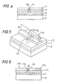
- the semiconductor device shown in Fig. 2 and Fig. 3 has a two-layered structure; that is, in a portion of the device shown in Fig. 3, two aluminium wirings 8 and 11 are on two levels and have an insulator layer 9 of PSG interposed between them and are thereby electrically insulated from each other.
- the lower aluminium wiring 8 is formed on another insulator layer 7 of silicon dioxide (SiO2) formed over a silicon substrate 6.
- the side wall 10a of the via hole has a cylindrical PSG surface which is electrically insulative, having a high resistance sufficient to maintain the electrical insulation between the two aluminium wirings 8 and 11.
- the side wall 10a may be partially covered by aluminium deposited during an aluminium sputtering deposition process preceding the lithographic patterning of the aluminium wiring 11.
- the above-described electrical insulation is maintained thanks to the high aspect ratio of the via hole 10 and proper selection of an oblique sputtering angle for the aluminium vapour, which creates an effective shadowing effect for the sputtering.
- An isotropic reactive gas etching process is suitable for providing overhanging side walls, as described later.
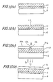
- Figs. 9(a) to (d) illustrate fabrication and activation of an activatable conductive link in accordance with the first embodiment of the present invention.
- the excimer laser employed may be, for example, a pulsed Ar F excimer laser (wavelength: 193 nm), having an energy density of 10 J/cm2 and a pulse width of 15 ns.
- one pulse shot is enough to activate the conductive link 10.
- a laser pulse shot of such high energy density and of such narrow pulse width serves to confine thermal diffusion to a small area in the vicinity of the irradiated target portion, preventing damage due to undesirable temperature increases, such as alloying of aluminium members with adjacent silicon members.
- excimer laser such as Kr F2 excimer lasers (wavelength: 248 nm), Xe excimer lasers (wavelength: 308 nm), are available for use in this field.
- a definitely effective method is to open a via hole after patterning the upper aluminium wiring 11.
- This method is described with reference to Figs. 11.
- an upper aluminium layer 11a, a PSG layer 9, a lower aluminium wiring 8, a silicon dioxide (SiO2) layer 7 and a silicon substrate 6 are laminated as illustrated, formed by conventional semiconductor device fabricating methods.
- the upper aluminium layer 11a is then patterned to form an upper aluminium wiring 11, as shown in Fig. 11(b), including a via hole pattern 10v opened amid the pattern of the upper aluminium wiring 11, at a predetermined location, by employing a mask (not shown).
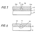
- the trench 13 plays an important role in the achievement of a reliable connection between the associated aluminium wirings. Melted aluminium flows into the trench, filling up the trench 13 and planarizing the cut portion between the wirings. The resulting connection is strong and stable. Without the trench 13, aluminium at the connecting point would overflow in the vicinity of the laser pulse irradiated portion, resulting in an unreliable connection between the wirings to be connected.
- the first conductive path may be made of metal, for example aluminium or aluminium alloy.
- the via hole may be a circular hole having an aspect ratio which is defined as a ratio of the depth to the inner diameter, higher than 1.0.
- the side wall of the via hole may be overhanging.
- the second conductive path may be a conductive doped region formed in a semiconductor substrate of said semiconductor device.
- the first conductive path and said second conductive path may be formed on said first insulating layer in the same level, said concaved portion being a trench having an insulative side wall and a mouth edge of which is in contact with said first conductive path and said second conductive path at mutually facing portions of said mouth edge.
- the first conductive path and said second conductive path may be arranged on said first insulating layer in the same level, said concaved portion being a trench having an insulative side wall.
- a conducting link disposed in an insulating layer of a semiconductor device in combination with a plurality of wirings of the device which are electrically separated from each other.
- the conductive link is selectively activated, providing the wirings with a conducting path, and is activatable by melting metal contained in the wirings by irradiating the portion in the vicinity of the link with a shot of a pulse of laser beam.
- the link comprises a via hole or a trench disposed in the insulating layer depending on the structural configuration of the device. The method of fabricating and activating the conductive link is provided.
Landscapes
- Internal Circuitry In Semiconductor Integrated Circuit Devices (AREA)
- Design And Manufacture Of Integrated Circuits (AREA)
Claims (15)
- Liaison conductrice activable dans un dispositif semi-conducteur, la structure comprenant dans son état non conducteur, non activé, un vide dans une couche isolante du dispositif semi-conducteur, en travers duquel vide des éléments conducteurs du dispositif se font face l'un à l'autre, le vide étant tel que le matériau conducteur ne s'étende pas jusqu'à une distance, par rapport aux parois intérieures du vide, telle qu'il établisse une connexion conductrice entre les éléments conducteurs, et telle que lors de l'activation de la liaison le matériau conducteur, d'au moins l'un des éléments conducteurs qui se font face, fonde et remplisse le vide pour établir une liaison conductrice entre les éléments conducteurs.
- Structure selon la revendication 1, dans laquelle au mois l'un des éléments conducteurs qui se font face, qui fond lors de l'activation, est fait de métal, par exemple de l'aluminium ou un alliage d'aluminium.
- Structure selon la revendication 1 ou 2, dans laquelle la couche isolante est faite de verre de phospho-silicate (PSG) ou de dioxyde de silicium.
- Structure selon la revendication 1, 2 ou 3, dans laquelle les éléments conducteurs qui se font face sont des éléments de couches conductrices situées, respectivement, une au-dessus de la couche isolante, une au-dessous de la couche isolante, ou sont, respectivement, un élément d'une couche conductrice au-dessus de la couche isolante et un élément d'une région de substrat de dispositif conducteur dopée au-dessous de la couche isolante, et le vide est un trou traversant qui traverse la couche isolante.
- Structure selon la revendication 1, 2 ou 3, dans laquelle les éléments conducteurs qui se font face sont tous les deux formés sur une surface supérieure de la couche isolante et dans laquelle le vide est une tranchée, une rainure ou un trou dans la couche isolante.
- Structure selon l'une quelconque des revendications précédentes dans laquelle les parois latérale du vide, défini par le matériau de la couche isolante, sont en surplomb.
- Structure selon l'une quelconque des revendications précédentes dans laquelle le vide a un rapport d'allongement, c'est-à-dire le rapport de la profondeur dans la couche isolante à la largeur de l'ouverture supérieure, de 1,0 ou davantage.
- Procédé de formation et d'activation d'une structure de liaison conductrice activable dans un dispositif semi-conducteur, le procédé comprenant :
la formation d'un vide dans une couche isolante du dispositif, avec des éléments conducteurs du dispositif qui se font face l'un à l'autre en travers du vide, pour créer une structure de liaison non conductrice, non activée, le vide étant tel que le matériau conducteur ne s'étende pas sur les parois intérieures du vide sur une distance telle qu'il établisse une connexion conductrice entre les éléments conducteurs, et
l'activation de la structure de liaison en chauffant localement une région dans le voisinage du vide, de tel manière que le matériau conducteur d'au moins l'un des éléments conducteurs fonde et remplisse le vide pour établir une liaison conductrice entre les éléments conducteurs. - Procédé selon la revendication 8, dans lequel l'échauffement local est réalisé en utilisant une impulsion de faisceau d'énergie, par exemple une impulsion de rayon laser excimer.
- Procédé selon la revendication 9, dans lequel une impulsion de rayon laser excimer d'une densité d'énergie dans la plage de 5 J/cm² à 12 J/cm², est utilisée
- Procédé selon l'une quelconque des revendications 8 à 10, dans lequel la couche isolante est formée sur l'un des éléments conducteurs qui peut appartenir à une couche conductrice ou à une région de substrat de dispositif conducteur dopée et l'autre élément conducteur est un élément d'une couche conductrice formée sur la couche isolante, le vide ayant la forme d'un trou traversant qui traverse la couche isolante.
- Procédé selon l'une quelconque des revendications 8 à 10, dans lequel les éléments conducteurs sont des éléments d'une couche conductrice formée sur la couche isolante et dans lequel le vide a la forme d'une tranchée, d'une fente ou d'un trou formés dans la couche isolante.
- Procédé selon l'une quelconque des revendications 8 à 12, dans lequel les parois latérales du vide , définies par le matériau de la couche isolante, sont formées de façon a être en surplomb, en utilisant un procédé de gravure réactive isotrope.
- Procédé selon l'une quelconque des revendications 8 à 13, dans lequel le vide dans la couche isolante est formé avant la formation de la couche conductrice sur la couche isolante.
- Procédé selon l'une quelconque des revendications 8 à 13, dans lequel le vide dans la couche isolante est formé après la formation de la couche conductrice sur la couche isolante, en utilisant une ouverture prévue dans la couche conductrice sous la forme d'un dessin pour graver le vide dans la couche isolante.
Applications Claiming Priority (2)
| Application Number | Priority Date | Filing Date | Title |
|---|---|---|---|
| JP189094/86 | 1986-08-12 | ||
| JP61189094A JPS6344739A (ja) | 1986-08-12 | 1986-08-12 | 半導体装置の製造方法 |
Publications (3)
| Publication Number | Publication Date |
|---|---|
| EP0256494A2 EP0256494A2 (fr) | 1988-02-24 |
| EP0256494A3 EP0256494A3 (en) | 1988-07-27 |
| EP0256494B1 true EP0256494B1 (fr) | 1993-01-07 |
Family
ID=16235236
Family Applications (1)
| Application Number | Title | Priority Date | Filing Date |
|---|---|---|---|
| EP87111603A Expired - Lifetime EP0256494B1 (fr) | 1986-08-12 | 1987-08-11 | Liens conducteurs activables pour dispositifs semi-conducteurs |
Country Status (5)
| Country | Link |
|---|---|
| US (1) | US4968643A (fr) |
| EP (1) | EP0256494B1 (fr) |
| JP (1) | JPS6344739A (fr) |
| KR (1) | KR910004038B1 (fr) |
| DE (1) | DE3783404T2 (fr) |
Families Citing this family (21)
| Publication number | Priority date | Publication date | Assignee | Title |
|---|---|---|---|---|
| US5070392A (en) * | 1988-03-18 | 1991-12-03 | Digital Equipment Corporation | Integrated circuit having laser-alterable metallization layer |
| US5250465A (en) * | 1991-01-28 | 1993-10-05 | Fujitsu Limited | Method of manufacturing semiconductor devices |
| US5451811A (en) * | 1991-10-08 | 1995-09-19 | Aptix Corporation | Electrically programmable interconnect element for integrated circuits |
| US5321322A (en) * | 1991-11-27 | 1994-06-14 | Aptix Corporation | Programmable interconnect architecture without active devices |
| WO1993012582A1 (fr) * | 1991-12-13 | 1993-06-24 | Knights Technology, Inc. | Dispositif logique programmable et procedes de fabrication |
| JPH0799791B2 (ja) * | 1992-04-15 | 1995-10-25 | インターナショナル・ビジネス・マシーンズ・コーポレイション | 透明基板上の回路ライン接続方法 |
| JPH06124913A (ja) * | 1992-06-26 | 1994-05-06 | Semiconductor Energy Lab Co Ltd | レーザー処理方法 |
| KR960009996B1 (ko) * | 1992-08-24 | 1996-07-25 | 금성일렉트론 주식회사 | 반도체 소자의 리페어장치 및 그 배치방법 |
| US5453402A (en) * | 1992-12-15 | 1995-09-26 | Advanced Micro Devices, Inc. | Selective metal via plug growth technology for deep sub-micrometer ULSI |
| JPH06260441A (ja) * | 1993-03-03 | 1994-09-16 | Nec Corp | 半導体装置の製造方法 |
| US5585602A (en) * | 1995-01-09 | 1996-12-17 | Massachusetts Institute Of Technology | Structure for providing conductive paths |
| US5940727A (en) * | 1994-10-11 | 1999-08-17 | Massachusetts Institute Of Technology | Technique for producing interconnecting conductive links |
| US5861325A (en) * | 1994-03-10 | 1999-01-19 | Massachusetts Institute Of Technology | Technique for producing interconnecting conductive links |
| KR100363410B1 (ko) | 1994-03-10 | 2003-02-11 | 메사추세츠 인스티튜트 오브 테크놀로지 | 상호접속용도전링크제조방법 |
| US5920789A (en) * | 1994-10-11 | 1999-07-06 | Massachusetts Institute Of Technology | Technique for producing interconnecting conductive links |
| TW278229B (en) * | 1994-12-29 | 1996-06-11 | Siemens Ag | Fuse structure for an integrated circuit device and method for manufacturing a fuse structure |
| JP3160198B2 (ja) * | 1995-02-08 | 2001-04-23 | インターナショナル・ビジネス・マシーンズ・コーポレ−ション | デカップリング・コンデンサが形成された半導体基板及びこれの製造方法 |
| US5731047A (en) * | 1996-11-08 | 1998-03-24 | W.L. Gore & Associates, Inc. | Multiple frequency processing to improve electrical resistivity of blind micro-vias |
| JPH10229125A (ja) * | 1997-02-14 | 1998-08-25 | Nec Corp | 半導体装置 |
| US6288437B1 (en) * | 1999-02-26 | 2001-09-11 | Micron Technology, Inc. | Antifuse structures methods and applications |
| US6472253B1 (en) | 1999-11-15 | 2002-10-29 | Vlsi Technology, Inc. | Programmable semiconductor device structures and methods for making the same |
Citations (1)
| Publication number | Priority date | Publication date | Assignee | Title |
|---|---|---|---|---|
| EP0251523A1 (fr) * | 1986-06-13 | 1988-01-07 | Fujitsu Limited | Méthode de fabrication d'un élément semi-conducteur ayant de bons contacts ohmiques entre une pluralité de couches d'interconnexion |
Family Cites Families (7)
| Publication number | Priority date | Publication date | Assignee | Title |
|---|---|---|---|---|
| JPS5780738A (en) * | 1980-11-07 | 1982-05-20 | Seiko Epson Corp | Semiconductor integrated device |
| US4585490A (en) * | 1981-12-07 | 1986-04-29 | Massachusetts Institute Of Technology | Method of making a conductive path in multi-layer metal structures by low power laser beam |
| JPS5996746A (ja) * | 1982-11-26 | 1984-06-04 | Hitachi Ltd | 半導体装置およびその製造方法 |
| ATE56310T1 (de) * | 1984-06-27 | 1990-09-15 | Contraves Ag | Verfahren zur herstellung eines basismaterials fuer eine hybridschaltung. |
| US4814578A (en) * | 1985-06-24 | 1989-03-21 | The United States Of America As Represented By The Department Of Energy | Planarization of metal films for multilevel interconnects |
| US4674176A (en) * | 1985-06-24 | 1987-06-23 | The United States Of America As Represented By The United States Department Of Energy | Planarization of metal films for multilevel interconnects by pulsed laser heating |
| US4681795A (en) * | 1985-06-24 | 1987-07-21 | The United States Of America As Represented By The Department Of Energy | Planarization of metal films for multilevel interconnects |
-
1986
- 1986-08-12 JP JP61189094A patent/JPS6344739A/ja active Granted
-
1987
- 1987-08-11 EP EP87111603A patent/EP0256494B1/fr not_active Expired - Lifetime
- 1987-08-11 KR KR1019870008776A patent/KR910004038B1/ko not_active Expired
- 1987-08-11 DE DE8787111603T patent/DE3783404T2/de not_active Expired - Fee Related
-
1989
- 1989-04-26 US US07/344,525 patent/US4968643A/en not_active Expired - Fee Related
Patent Citations (1)
| Publication number | Priority date | Publication date | Assignee | Title |
|---|---|---|---|---|
| EP0251523A1 (fr) * | 1986-06-13 | 1988-01-07 | Fujitsu Limited | Méthode de fabrication d'un élément semi-conducteur ayant de bons contacts ohmiques entre une pluralité de couches d'interconnexion |
Also Published As
| Publication number | Publication date |
|---|---|
| JPS6344739A (ja) | 1988-02-25 |
| KR910004038B1 (ko) | 1991-06-22 |
| US4968643A (en) | 1990-11-06 |
| KR880003407A (ko) | 1988-05-17 |
| DE3783404T2 (de) | 1993-05-06 |
| EP0256494A2 (fr) | 1988-02-24 |
| EP0256494A3 (en) | 1988-07-27 |
| DE3783404D1 (de) | 1993-02-18 |
| JPH058864B2 (fr) | 1993-02-03 |
Similar Documents
| Publication | Publication Date | Title |
|---|---|---|
| EP0256494A2 (fr) | Liens conducteurs activables pour dispositifs semi-conducteurs | |
| EP0112675B1 (fr) | Structure de pont activable sélectivement pour former une connexion conductrice dans un circuit intégré | |
| EP0083211B1 (fr) | Dispositif semi-conducteur comprenant un fusible | |
| US5663590A (en) | Product of process for formation of vias (or contact openings) and fuses in the same insulation layer with minimal additional steps | |
| EP0128675B1 (fr) | Procédé de fabrication d'un circuit intégré à métallisation multicouche avec un fusible et une ouverture pour le fusible | |
| CA1286795C (fr) | Fabrication de trajets conducteurs intercouches dans les circuits integres | |
| US4740485A (en) | Method for forming a fuse | |
| US4916809A (en) | Method for programmable laser connection of two superimposed conductors of the interconnect system of an integrated circuit | |
| US5753539A (en) | Method of making an integrated circuit with windowed fuse element and contact pad | |
| US5235205A (en) | Laser trimmed integrated circuit | |
| US6335228B1 (en) | Method for making an anti-fuse | |
| JP2728412B2 (ja) | 半導体装置 | |
| JPH10270566A (ja) | レーザ溶断導線を有する固体回路とその固体回路の製造方法 | |
| EP1285463A2 (fr) | Fusibles ameliores par degradation locale de l'element de fusible | |
| US5652169A (en) | Method for fabricating a programmable semiconductor element having an antifuse structure | |
| US5789794A (en) | Fuse structure for an integrated circuit element | |
| KR900002084B1 (ko) | 반도체장치 | |
| EP0581867A1 (fr) | Procede d'ajustage au laser et circuit integre resultant | |
| KR0146284B1 (ko) | 반도체 기판상의 가용성 링크 제조방법 | |
| US4673592A (en) | Metal planarization process | |
| US20020008236A1 (en) | Electronic device, and method of patterning a first layer | |
| JPH079942B2 (ja) | 集積回路の基板のドーピングされた領域に導体をレーザによって接続する方法と、該方法を実施して得られる集積回路 | |
| JPH04307757A (ja) | 半導体装置およびその製造方法 | |
| EP0258962A2 (fr) | Dispositifs semi-conducteurs à liens sélectifs et un procédé pour leur fabrication | |
| JPH0645448A (ja) | 半導体装置 |
Legal Events
| Date | Code | Title | Description |
|---|---|---|---|
| PUAI | Public reference made under article 153(3) epc to a published international application that has entered the european phase |
Free format text: ORIGINAL CODE: 0009012 |
|
| AK | Designated contracting states |
Kind code of ref document: A2 Designated state(s): DE FR GB |
|
| PUAL | Search report despatched |
Free format text: ORIGINAL CODE: 0009013 |
|
| AK | Designated contracting states |
Kind code of ref document: A3 Designated state(s): DE FR GB |
|
| 17P | Request for examination filed |
Effective date: 19881121 |
|
| 17Q | First examination report despatched |
Effective date: 19900523 |
|
| GRAA | (expected) grant |
Free format text: ORIGINAL CODE: 0009210 |
|
| AK | Designated contracting states |
Kind code of ref document: B1 Designated state(s): DE FR GB |
|
| REF | Corresponds to: |
Ref document number: 3783404 Country of ref document: DE Date of ref document: 19930218 |
|
| ET | Fr: translation filed | ||
| PG25 | Lapsed in a contracting state [announced via postgrant information from national office to epo] |
Ref country code: GB Effective date: 19930811 |
|
| PLBE | No opposition filed within time limit |
Free format text: ORIGINAL CODE: 0009261 |
|
| 26N | No opposition filed | ||
| GBPC | Gb: european patent ceased through non-payment of renewal fee |
Effective date: 19930811 |
|
| PG25 | Lapsed in a contracting state [announced via postgrant information from national office to epo] |
Ref country code: FR Effective date: 19940429 |
|
| PG25 | Lapsed in a contracting state [announced via postgrant information from national office to epo] |
Ref country code: DE Effective date: 19940503 |
|
| REG | Reference to a national code |
Ref country code: FR Ref legal event code: ST |