EP0272140A2 - Procèdè de dèpÔt chimique en phase vapeur à l'aide d'un plasma de dioxyde de silicium à partir de TEOS. - Google Patents
Procèdè de dèpÔt chimique en phase vapeur à l'aide d'un plasma de dioxyde de silicium à partir de TEOS. Download PDFInfo
- Publication number
- EP0272140A2 EP0272140A2 EP87311193A EP87311193A EP0272140A2 EP 0272140 A2 EP0272140 A2 EP 0272140A2 EP 87311193 A EP87311193 A EP 87311193A EP 87311193 A EP87311193 A EP 87311193A EP 0272140 A2 EP0272140 A2 EP 0272140A2
- Authority
- EP
- European Patent Office
- Prior art keywords
- wafer
- gas
- chamber
- deposition
- manifold
- Prior art date
- Legal status (The legal status is an assumption and is not a legal conclusion. Google has not performed a legal analysis and makes no representation as to the accuracy of the status listed.)
- Granted
Links
Images


Classifications
-
- H—ELECTRICITY
- H10—SEMICONDUCTOR DEVICES; ELECTRIC SOLID-STATE DEVICES NOT OTHERWISE PROVIDED FOR
- H10P—GENERIC PROCESSES OR APPARATUS FOR THE MANUFACTURE OR TREATMENT OF DEVICES COVERED BY CLASS H10
- H10P14/00—Formation of materials, e.g. in the shape of layers or pillars
- H10P14/60—Formation of materials, e.g. in the shape of layers or pillars of insulating materials
- H10P14/63—Formation of materials, e.g. in the shape of layers or pillars of insulating materials characterised by the formation processes
- H10P14/6326—Deposition processes
- H10P14/6328—Deposition from the gas or vapour phase
- H10P14/6334—Deposition from the gas or vapour phase using decomposition or reaction of gaseous or vapour phase compounds, i.e. chemical vapour deposition
- H10P14/6336—Deposition from the gas or vapour phase using decomposition or reaction of gaseous or vapour phase compounds, i.e. chemical vapour deposition in the presence of a plasma [PECVD]
-
- C—CHEMISTRY; METALLURGY
- C23—COATING METALLIC MATERIAL; COATING MATERIAL WITH METALLIC MATERIAL; CHEMICAL SURFACE TREATMENT; DIFFUSION TREATMENT OF METALLIC MATERIAL; COATING BY VACUUM EVAPORATION, BY SPUTTERING, BY ION IMPLANTATION OR BY CHEMICAL VAPOUR DEPOSITION, IN GENERAL; INHIBITING CORROSION OF METALLIC MATERIAL OR INCRUSTATION IN GENERAL
- C23C—COATING METALLIC MATERIAL; COATING MATERIAL WITH METALLIC MATERIAL; SURFACE TREATMENT OF METALLIC MATERIAL BY DIFFUSION INTO THE SURFACE, BY CHEMICAL CONVERSION OR SUBSTITUTION; COATING BY VACUUM EVAPORATION, BY SPUTTERING, BY ION IMPLANTATION OR BY CHEMICAL VAPOUR DEPOSITION, IN GENERAL
- C23C16/00—Chemical coating by decomposition of gaseous compounds, without leaving reaction products of surface material in the coating, i.e. chemical vapour deposition [CVD] processes
- C23C16/22—Chemical coating by decomposition of gaseous compounds, without leaving reaction products of surface material in the coating, i.e. chemical vapour deposition [CVD] processes characterised by the deposition of inorganic material, other than metallic material
- C23C16/30—Deposition of compounds, mixtures or solid solutions, e.g. borides, carbides, nitrides
- C23C16/40—Oxides
- C23C16/401—Oxides containing silicon
- C23C16/402—Silicon dioxide
-
- C—CHEMISTRY; METALLURGY
- C23—COATING METALLIC MATERIAL; COATING MATERIAL WITH METALLIC MATERIAL; CHEMICAL SURFACE TREATMENT; DIFFUSION TREATMENT OF METALLIC MATERIAL; COATING BY VACUUM EVAPORATION, BY SPUTTERING, BY ION IMPLANTATION OR BY CHEMICAL VAPOUR DEPOSITION, IN GENERAL; INHIBITING CORROSION OF METALLIC MATERIAL OR INCRUSTATION IN GENERAL
- C23C—COATING METALLIC MATERIAL; COATING MATERIAL WITH METALLIC MATERIAL; SURFACE TREATMENT OF METALLIC MATERIAL BY DIFFUSION INTO THE SURFACE, BY CHEMICAL CONVERSION OR SUBSTITUTION; COATING BY VACUUM EVAPORATION, BY SPUTTERING, BY ION IMPLANTATION OR BY CHEMICAL VAPOUR DEPOSITION, IN GENERAL
- C23C16/00—Chemical coating by decomposition of gaseous compounds, without leaving reaction products of surface material in the coating, i.e. chemical vapour deposition [CVD] processes
- C23C16/44—Chemical coating by decomposition of gaseous compounds, without leaving reaction products of surface material in the coating, i.e. chemical vapour deposition [CVD] processes characterised by the method of coating
- C23C16/455—Chemical coating by decomposition of gaseous compounds, without leaving reaction products of surface material in the coating, i.e. chemical vapour deposition [CVD] processes characterised by the method of coating characterised by the method used for introducing gases into reaction chamber or for modifying gas flows in reaction chamber
- C23C16/45519—Inert gas curtains
- C23C16/45521—Inert gas curtains the gas, other than thermal contact gas, being introduced the rear of the substrate to flow around its periphery
-
- C—CHEMISTRY; METALLURGY
- C23—COATING METALLIC MATERIAL; COATING MATERIAL WITH METALLIC MATERIAL; CHEMICAL SURFACE TREATMENT; DIFFUSION TREATMENT OF METALLIC MATERIAL; COATING BY VACUUM EVAPORATION, BY SPUTTERING, BY ION IMPLANTATION OR BY CHEMICAL VAPOUR DEPOSITION, IN GENERAL; INHIBITING CORROSION OF METALLIC MATERIAL OR INCRUSTATION IN GENERAL
- C23C—COATING METALLIC MATERIAL; COATING MATERIAL WITH METALLIC MATERIAL; SURFACE TREATMENT OF METALLIC MATERIAL BY DIFFUSION INTO THE SURFACE, BY CHEMICAL CONVERSION OR SUBSTITUTION; COATING BY VACUUM EVAPORATION, BY SPUTTERING, BY ION IMPLANTATION OR BY CHEMICAL VAPOUR DEPOSITION, IN GENERAL
- C23C16/00—Chemical coating by decomposition of gaseous compounds, without leaving reaction products of surface material in the coating, i.e. chemical vapour deposition [CVD] processes
- C23C16/44—Chemical coating by decomposition of gaseous compounds, without leaving reaction products of surface material in the coating, i.e. chemical vapour deposition [CVD] processes characterised by the method of coating
- C23C16/455—Chemical coating by decomposition of gaseous compounds, without leaving reaction products of surface material in the coating, i.e. chemical vapour deposition [CVD] processes characterised by the method of coating characterised by the method used for introducing gases into reaction chamber or for modifying gas flows in reaction chamber
- C23C16/45563—Gas nozzles
- C23C16/45565—Shower nozzles
-
- C—CHEMISTRY; METALLURGY
- C23—COATING METALLIC MATERIAL; COATING MATERIAL WITH METALLIC MATERIAL; CHEMICAL SURFACE TREATMENT; DIFFUSION TREATMENT OF METALLIC MATERIAL; COATING BY VACUUM EVAPORATION, BY SPUTTERING, BY ION IMPLANTATION OR BY CHEMICAL VAPOUR DEPOSITION, IN GENERAL; INHIBITING CORROSION OF METALLIC MATERIAL OR INCRUSTATION IN GENERAL
- C23C—COATING METALLIC MATERIAL; COATING MATERIAL WITH METALLIC MATERIAL; SURFACE TREATMENT OF METALLIC MATERIAL BY DIFFUSION INTO THE SURFACE, BY CHEMICAL CONVERSION OR SUBSTITUTION; COATING BY VACUUM EVAPORATION, BY SPUTTERING, BY ION IMPLANTATION OR BY CHEMICAL VAPOUR DEPOSITION, IN GENERAL
- C23C16/00—Chemical coating by decomposition of gaseous compounds, without leaving reaction products of surface material in the coating, i.e. chemical vapour deposition [CVD] processes
- C23C16/44—Chemical coating by decomposition of gaseous compounds, without leaving reaction products of surface material in the coating, i.e. chemical vapour deposition [CVD] processes characterised by the method of coating
- C23C16/50—Chemical coating by decomposition of gaseous compounds, without leaving reaction products of surface material in the coating, i.e. chemical vapour deposition [CVD] processes characterised by the method of coating using electric discharges
- C23C16/505—Chemical coating by decomposition of gaseous compounds, without leaving reaction products of surface material in the coating, i.e. chemical vapour deposition [CVD] processes characterised by the method of coating using electric discharges using radio frequency discharges
- C23C16/509—Chemical coating by decomposition of gaseous compounds, without leaving reaction products of surface material in the coating, i.e. chemical vapour deposition [CVD] processes characterised by the method of coating using electric discharges using radio frequency discharges using internal electrodes
- C23C16/5096—Flat-bed apparatus
-
- C—CHEMISTRY; METALLURGY
- C23—COATING METALLIC MATERIAL; COATING MATERIAL WITH METALLIC MATERIAL; CHEMICAL SURFACE TREATMENT; DIFFUSION TREATMENT OF METALLIC MATERIAL; COATING BY VACUUM EVAPORATION, BY SPUTTERING, BY ION IMPLANTATION OR BY CHEMICAL VAPOUR DEPOSITION, IN GENERAL; INHIBITING CORROSION OF METALLIC MATERIAL OR INCRUSTATION IN GENERAL
- C23C—COATING METALLIC MATERIAL; COATING MATERIAL WITH METALLIC MATERIAL; SURFACE TREATMENT OF METALLIC MATERIAL BY DIFFUSION INTO THE SURFACE, BY CHEMICAL CONVERSION OR SUBSTITUTION; COATING BY VACUUM EVAPORATION, BY SPUTTERING, BY ION IMPLANTATION OR BY CHEMICAL VAPOUR DEPOSITION, IN GENERAL
- C23C16/00—Chemical coating by decomposition of gaseous compounds, without leaving reaction products of surface material in the coating, i.e. chemical vapour deposition [CVD] processes
- C23C16/44—Chemical coating by decomposition of gaseous compounds, without leaving reaction products of surface material in the coating, i.e. chemical vapour deposition [CVD] processes characterised by the method of coating
- C23C16/54—Apparatus specially adapted for continuous coating
-
- H—ELECTRICITY
- H01—ELECTRIC ELEMENTS
- H01J—ELECTRIC DISCHARGE TUBES OR DISCHARGE LAMPS
- H01J37/00—Discharge tubes with provision for introducing objects or material to be exposed to the discharge, e.g. for the purpose of examination or processing thereof
- H01J37/32—Gas-filled discharge tubes
- H01J37/32009—Arrangements for generation of plasma specially adapted for examination or treatment of objects, e.g. plasma sources
- H01J37/32082—Radio frequency generated discharge
-
- H—ELECTRICITY
- H01—ELECTRIC ELEMENTS
- H01J—ELECTRIC DISCHARGE TUBES OR DISCHARGE LAMPS
- H01J37/00—Discharge tubes with provision for introducing objects or material to be exposed to the discharge, e.g. for the purpose of examination or processing thereof
- H01J37/32—Gas-filled discharge tubes
- H01J37/32431—Constructional details of the reactor
- H01J37/3244—Gas supply means
-
- H—ELECTRICITY
- H10—SEMICONDUCTOR DEVICES; ELECTRIC SOLID-STATE DEVICES NOT OTHERWISE PROVIDED FOR
- H10P—GENERIC PROCESSES OR APPARATUS FOR THE MANUFACTURE OR TREATMENT OF DEVICES COVERED BY CLASS H10
- H10P14/00—Formation of materials, e.g. in the shape of layers or pillars
- H10P14/60—Formation of materials, e.g. in the shape of layers or pillars of insulating materials
- H10P14/66—Formation of materials, e.g. in the shape of layers or pillars of insulating materials characterised by the type of materials
- H10P14/668—Formation of materials, e.g. in the shape of layers or pillars of insulating materials characterised by the type of materials the materials being characterised by the deposition precursor materials
- H10P14/6681—Formation of materials, e.g. in the shape of layers or pillars of insulating materials characterised by the type of materials the materials being characterised by the deposition precursor materials the precursor containing a compound comprising Si
- H10P14/6682—Formation of materials, e.g. in the shape of layers or pillars of insulating materials characterised by the type of materials the materials being characterised by the deposition precursor materials the precursor containing a compound comprising Si the compound being a silane, e.g. disilane, methylsilane or chlorosilane
-
- H—ELECTRICITY
- H10—SEMICONDUCTOR DEVICES; ELECTRIC SOLID-STATE DEVICES NOT OTHERWISE PROVIDED FOR
- H10P—GENERIC PROCESSES OR APPARATUS FOR THE MANUFACTURE OR TREATMENT OF DEVICES COVERED BY CLASS H10
- H10P14/00—Formation of materials, e.g. in the shape of layers or pillars
- H10P14/60—Formation of materials, e.g. in the shape of layers or pillars of insulating materials
- H10P14/66—Formation of materials, e.g. in the shape of layers or pillars of insulating materials characterised by the type of materials
- H10P14/668—Formation of materials, e.g. in the shape of layers or pillars of insulating materials characterised by the type of materials the materials being characterised by the deposition precursor materials
- H10P14/6681—Formation of materials, e.g. in the shape of layers or pillars of insulating materials characterised by the type of materials the materials being characterised by the deposition precursor materials the precursor containing a compound comprising Si
- H10P14/6684—Formation of materials, e.g. in the shape of layers or pillars of insulating materials characterised by the type of materials the materials being characterised by the deposition precursor materials the precursor containing a compound comprising Si the compound comprising silicon and oxygen
- H10P14/6686—Formation of materials, e.g. in the shape of layers or pillars of insulating materials characterised by the type of materials the materials being characterised by the deposition precursor materials the precursor containing a compound comprising Si the compound comprising silicon and oxygen the compound being a molecule comprising at least one silicon-oxygen bond and the compound having hydrogen or an organic group attached to the silicon or oxygen, e.g. a siloxane
-
- H—ELECTRICITY
- H10—SEMICONDUCTOR DEVICES; ELECTRIC SOLID-STATE DEVICES NOT OTHERWISE PROVIDED FOR
- H10P—GENERIC PROCESSES OR APPARATUS FOR THE MANUFACTURE OR TREATMENT OF DEVICES COVERED BY CLASS H10
- H10P14/00—Formation of materials, e.g. in the shape of layers or pillars
- H10P14/60—Formation of materials, e.g. in the shape of layers or pillars of insulating materials
- H10P14/69—Inorganic materials
- H10P14/692—Inorganic materials composed of oxides, glassy oxides or oxide-based glasses
- H10P14/6921—Inorganic materials composed of oxides, glassy oxides or oxide-based glasses containing silicon
- H10P14/69215—Inorganic materials composed of oxides, glassy oxides or oxide-based glasses containing silicon the material being a silicon oxide, e.g. SiO2
-
- H—ELECTRICITY
- H10—SEMICONDUCTOR DEVICES; ELECTRIC SOLID-STATE DEVICES NOT OTHERWISE PROVIDED FOR
- H10P—GENERIC PROCESSES OR APPARATUS FOR THE MANUFACTURE OR TREATMENT OF DEVICES COVERED BY CLASS H10
- H10P14/00—Formation of materials, e.g. in the shape of layers or pillars
- H10P14/60—Formation of materials, e.g. in the shape of layers or pillars of insulating materials
- H10P14/69—Inorganic materials
- H10P14/692—Inorganic materials composed of oxides, glassy oxides or oxide-based glasses
- H10P14/6921—Inorganic materials composed of oxides, glassy oxides or oxide-based glasses containing silicon
- H10P14/6922—Inorganic materials composed of oxides, glassy oxides or oxide-based glasses containing silicon the material containing Si, O and at least one of H, N, C, F or other non-metal elements, e.g. SiOC, SiOC:H or SiONC
- H10P14/6923—Inorganic materials composed of oxides, glassy oxides or oxide-based glasses containing silicon the material containing Si, O and at least one of H, N, C, F or other non-metal elements, e.g. SiOC, SiOC:H or SiONC the material being boron or phosphorus doped silicon oxides, e.g. BPSG, BSG or PSG
-
- H—ELECTRICITY
- H10—SEMICONDUCTOR DEVICES; ELECTRIC SOLID-STATE DEVICES NOT OTHERWISE PROVIDED FOR
- H10P—GENERIC PROCESSES OR APPARATUS FOR THE MANUFACTURE OR TREATMENT OF DEVICES COVERED BY CLASS H10
- H10P14/00—Formation of materials, e.g. in the shape of layers or pillars
- H10P14/60—Formation of materials, e.g. in the shape of layers or pillars of insulating materials
- H10P14/69—Inorganic materials
- H10P14/692—Inorganic materials composed of oxides, glassy oxides or oxide-based glasses
- H10P14/6921—Inorganic materials composed of oxides, glassy oxides or oxide-based glasses containing silicon
- H10P14/6922—Inorganic materials composed of oxides, glassy oxides or oxide-based glasses containing silicon the material containing Si, O and at least one of H, N, C, F or other non-metal elements, e.g. SiOC, SiOC:H or SiONC
- H10P14/6924—Inorganic materials composed of oxides, glassy oxides or oxide-based glasses containing silicon the material containing Si, O and at least one of H, N, C, F or other non-metal elements, e.g. SiOC, SiOC:H or SiONC the material being halogen doped silicon oxides, e.g. FSG
Definitions
- the present invention relates to a reactor and methods for performing single and in-situ multiple integrated circuit processing steps, including thermal CVD, plasma-enhanced chemical vapor deposition (PECVD), reactor self-cleaning, film etchback, and modification of profile or other film property by sputtering.
- the present invention also relates to a process for forming conformal, planar dielectric layers on integrated circuit wafers and to an in-situ multi-step process for forming conformal, planar dielectric layers that are suitable for use as interlevel dielectrics for multi-layer metallization interconnects.
- the early gas chemistry deposition reactors that were applied to semiconductor integrated circuit fabrication used relatively high temperature, thermally-activated chemistry to deposit from a gas onto a heated substrate.
- Such chemical vapor deposition of a solid onto a surface involves a heterogeneous surface reaction of gaseous species that adsorb onto the surface.
- the rate of film growth and the film quality depend on the wafer surface temperature and on the gaseous species available.
- low temperature plasma-enhanced deposition and etching techniques have been developed for forming diverse materials, including metals such as aluminum and tungsten, dielectric films such as silicon nitride and silicon dioxide, and semiconductor films such as silicon.
- the plasma used in the available plasma-enhanced chemical vapor deposition processes is a low pressure reactant gas discharge which is developed in an RF field.
- the plasma is, by definition, an electrically neutral ionized gas in which there are equal number densities of electrons and ions.
- the discharge is in the "glow" region and the electron energies can be quite high relative to heavy particle energies.
- the very high electron temperatures increase the density of disassociated species within the plasma which are available for deposition on nearby surfaces (such as substrates).
- the enhanced supply of reactive free radicals in the PECVD processes makes possible the deposition of dense, good quality films at lower temperatures and at faster deposition rates (300-400 Angstroms per minute) than are typically possible using purely thermally-activated CVD processes (100-200 Angstroms per minute).
- the deposition rates available using conventional plasma-enhanced processes are still relatively low.
- batch-type reactors are used in most commercial PECVD applications.
- the batch reactors process a relatively large number of wafers at once and, thus, provide relatively high throughput despite the low deposition rates.
- single-wafer reactors have certain advantages, such as the lack of within-batch uniformity problems, which make such reactors attractive, particularly for large, expensive wafers such as 5-8 inch diameter wafers.
- IC integrated circuit
- LSI large scale integration
- VLSI very large scale integration
- ULSI ultra-large integration
- This advancement in monolithic circuit integration has been made possible by improvements in the manufacturing equipment as well as in the materials and methods used in processing semiconductor wafers into IC chips.
- the incorporation into IC chips of, first, increasingly complex devices and circuits and, second, greater device densities and smaller minimum feature sizes and smaller separations imposes increasingly stringent requirements on the basic integrated circuit fabrication steps of masking, film formation, doping and etching.
- MOS metal oxide semiconductor
- MOS logic circuits may well use two to three metal interconnect layers and bipolar digital circuits may require three to four such layers.
- the increasing complexity, thickness/depth and small size of such multiple interconnect levels make it increasingly difficult to fabricate the required conformal, planar interlevel dielectric layers materials such as silicon dioxide that support and electrically isolate such metal interconnect layers.
- FIG. 16 The difficulty in forming planarized conformal coatings on small stepped surface topographies is illustrated in FIG. 16.
- a first film such as a conductor layer 171 has been formed over the existing stepped topography of a partially completed integrated circuit (not shown) and is undergoing the deposition of an interlayer dielectric layer 172 such as silicon dioxide. This is done preparatory to the formation of a second level conductor layer (not shown).
- the deposition rates at the bottom 173, the sides 174 and the top 175 of the stepped topography are proportional to the associated arrival angles.
- the bottom and side arrival angles are a function of and are limited by the depth and small width of the trench.
- the thickness of the bottom layer 173 tends to be deposited to a lesser thickness than is the side layer 174 which, in turn, is less than the thickness of top layer 175.
- Increasing the pressure used in the deposition process typically will increase the collision rate of the active species and decrease the mean-free path. This would increase the arrival angles and, thus, increase the deposition rate at the sidewalls 714 and bottom 173 of the trench or step. However, and referring to FIG. 17A, this also increases the arrival angle and associated deposition rate at stepped corners 176.
- the resulting inwardly sloping film configuration forms cusps 177-177 at the sidewall-bottom interface. It is difficult to form conformal metal and/or dielectric layers over such topographies. As a consequence, it is necessary to separately planarize the topography.
- the increased deposition rate at the corner 176 encloses a void 178.
- Such voids are exposed by subsequent planarization procedures and may allow the second level conductor to penetrate and run along the void and short the conductors and devices along the void.
- Another object is to provide the above-described versatile process characteristics along with the ability to vary the process sequence and the number of steps, including but not limited to the addition of reactor self-cleaning.
- our invention relates to a semiconductor processing reactor defining a chamber for mounting a wafer therein and an inlet gas manifold for supplying reactant gases to the wafer.
- the chamber also incorporates a uniform radial pumping system which includes vacuum exhaust pump means; a gas distributor plate mounted peripherally about the wafer mounting position within the chamber and including a circular array of exhaust holes therein; and a circular channel beneath and communicating with the hole array and having at least a single point connection to the vacuum exhaust pump for flowing gases radially from the inlet manifold across the wafer and through the exhaust port.
- the channel is of sufficiently large volume and conductance relative to the holes to enable controlled uniform radial gas flow across the wafer to the exhaust holes, thereby promoting uniform flow and processing (etching and deposition) over a wide range of pressures, including very high pressures up to about one atmosphere.
- the present invention is directed to a semiconductor processing reactor which comprises a housing forming a chamber for mounting a wafer horizontally, a vacuum exhaust pumping system communicating with the chamber, and an inlet gas manifold oriented horizontally over the wafer mounting position.
- the manifold has a central array of process gas apertures configured for dispensing reactant gas uniformly over the wafer and a second peripheral array of purging gas apertures configured for directing purging gas downward to the periphery of the wafer.
- the hole arrays are also arranged to eliminate radial alignment of holes.
- the reactor incorporates a system for circulating fluid of controlled temperature within the manifold for maintaining the internal surfaces within a selected temperature range to prevent condensation and reactions within the manifold and for maintaining the external manifold surfaces above a selected temperature range for eliminating unwanted deposition thereon.
- the reactor of the present invention comprises a thin susceptor for supporting a wafer, susceptor support means for mounting the susceptor in a horizontal position precisely parallel to the gas inlet manifold and means for selectively moving the wafer support means vertically to position the susceptor and support parallel to the gas manifold at selected variable-distance positions closely adjacent the gas manifold.
- the variable parallel close spacing can be 0.5 centimeter and smaller.
- the semiconductor processing reactor of the present invention comprises a housing defining a chamber therein adapted for the gas chemistry processing of a wafer positioned within the chamber.
- a transparent window forms the bottom of the chamber.
- a thin high emissivity susceptor is used for supporting a wafer within the chamber.
- a radiant heating module comprising a circular array of lamps mounted in a reflector module is mounted outside the housing for directing a substantially collimated beam of near-infrared radiant energy through the window onto the susceptor with an incident power density substantially higher at the edge of the susceptor than at the center thereof, to heat the wafer uniformly.
- a second, purge gas manifold is positioned beneath the wafer processing area for providing purging gas flow across the window and upward and across the bottom of the wafer.
- the combination of the high pressure, the purge flow from the inlet gas manifold and that from the purge gas manifold substantially eliminates deposition on chamber surfaces.
- the reactor of the present invention comprises a deposition gas feed-through device connected to the gas inlet manifold which comprises tube means adapted for providing co-axial flow of deposition gas on the inside of the tube and purge gas on the outside thereof into the gas inlet manifold.
- the tube is adapted for connection to ground at the inlet end and to an RF power supply at the outlet or manifold end to provide RF power to the manifold, and has a controlled electrical impedance along its length from the inlet to the outlet end for establishing a constant voltage gradient to prevent breakdown of the gas even at high RF frequencies and voltages.
- the features permit reactor operation over a wide pressure regime, that is, over a wide of pressures including high pressures up to approximately one atmosphere.
- the features also provide uniform susceptor and wafer temperatures, including both absolute temperature uniformity and spatial uniformity across the susceptor/wafer; uniform gas flow distribution across the wafer; and effective purging.
- the variable parallel close spacing between the electrodes adapts the reactor to various processes.
- the present invention also relates to a method for depositing a conformal layer of silicon dioxide onto a substrate by exposing the substrate to a reactive species formed from ozone, oxygen, tetraethylorthosilicate, and a carrier gas within a vacuum chamber, using a total gas pressure within the chamber 10 torr to 200 torr and a substrate temperature within the range of about 200°C to 500°C.
- a substrate temperature of about 375°C ⁇ 20°C is used to obtain maximum deposition rates and the chamber pressure is about 40 torr to 120 torr.
- the present invention is embodied in a method for depositing silicon dioxide onto a film or substrate by exposing the substrate to the plasma formed from tetraethylorthosilicate, oxygen and a carrier gas in a chamber using a total gas pressure within the range of about 1 to 50 torr, and a substrate temperature in the range of about 200°C to 500°C.
- the chamber pressure is 8-12 torr and the substrate temperature is about 375°C ⁇ 20°C.
- the invention is directed to a method for isotropically etching a silicon dioxide surface comprising the step of exposing a silicon dioxide surface to a plasma formed from fluorinate gas such as NF3, CF4 and C2F6 in a carrier gas in a chamber using a wafer temperature in the range of from about 200°C to 500°C.
- the chamber pressure is within the range of about 200 mT to 20 torr, and 500 mT to 10 torr.
- the invention is also embodied in a method for planarizing a non-planar dielectric coating or composite within a vacuum chamber by depositing a conformal layer of silicon dioxide onto the coating by exposing the coating to a reactive species formed from ozone, oxygen, tetraethylorthosilicate and a carrier gas, the total chamber gas pressure being within the approximate range 10 torr to 200 torr and the substrate temperature being within the approximate range 200°C to 500°C, to thereby form a composite of the conformal layer on the substrate; and isotropically etching the outer surface of the resulting composite layer.
- this planarizing process uses the plasma oxide deposition to first form a layer of silicon oxide and also uses the isotropic etch described above.
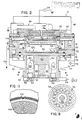
- FIGS. 1 and 2 are, respectively, a top plan view of the preferred embodiment of the single wafer, reactor 10 of our present invention, shown with the cover pivoted open, and a vertical cross-section of the reactor 10.
- the reactor system 10 comprises a housing 12 (also termed a "chamber"), typically made of aluminum, which defines an inner vacuum chamber 13 that has a plasma processing region 14 (FIG. 6).
- the reactor system 10 also includes a wafer-holding susceptor 16 and a unique wafer transport system 18 (FIG. 1) that includes vertically movable wafer support fingers 20 and susceptor support fingers 22. These fingers cooperate with an external robotic blade 24 (FIG. 1) for introducing wafers 15 into the process region or chamber 14 and depositing the wafers 15 on the susceptor 16 for processing, then removing the wafers 15 from the susceptor 16 and the chamber 12.
- the reactor system 10 further comprises a process/purge gas manifold or "box" 26 that applies process gas and purging gas to the chamber 13, an RF power supply and matching network 28 for creating and sustaining a process plasma from the inlet gas and a lamp heating system 30 for heating the susceptor 16 and wafer 15 positioned on the susceptor to effect deposition onto the wafer.
- a process/purge gas manifold or "box” 26 that applies process gas and purging gas to the chamber 13
- an RF power supply and matching network 28 for creating and sustaining a process plasma from the inlet gas
- a lamp heating system 30 for heating the susceptor 16 and wafer 15 positioned on the susceptor to effect deposition onto the wafer.
- high frequency RF power of 13.56 MHz is used, but low frequencies can be used.
- the gas manifold 26 is part of a unique process and purge gas distribution system 32 (FIGS. 2 and 10) that is designed to flow the process gas evenly radially outwardly across the wafer 15 to promote even deposition across the wafer and to purge the spent gas and entrained products radially outwardly from the edge of the wafer 15 at both the top and bottom thereof to substantially eliminate deposition on (and within) the gas manifold or box 26 and the chamber 12.
- a unique process and purge gas distribution system 32 (FIGS. 2 and 10) that is designed to flow the process gas evenly radially outwardly across the wafer 15 to promote even deposition across the wafer and to purge the spent gas and entrained products radially outwardly from the edge of the wafer 15 at both the top and bottom thereof to substantially eliminate deposition on (and within) the gas manifold or box 26 and the chamber 12.
- a liquid cooling system 34 controls the temperature of the components of the chamber 12 including, in particular, the temperature of the gas manifold or box 26.
- the temperature of the gas box components is selected to eliminate premature deposition within the gas box/manifold 26 upstream from the process chamber 14.
- the reactor system 10 includes a unique, RF/gas feed-through device 36 (FIGS. 2 and 12) that supplies process and purge gas to the RF-driven gas manifold 26 from an electrically ground supply.
- RF energy to the gas box or manifold 26 has the advantage of the wafer residing on the grounded counter electrode or susceptor 16, which makes possible a high degree of plasma confinement that would not be achievable if the RF energy were applied to the wafer and the gas box were grounded.
- the hardware is mechanically and electrically simpler since electrical isolation between wafer/susceptor and chamber is not required (or permitted). Temperature measurement and control of the susceptor/wafer in the presence of high frequency electric and magnetic fields is greatly simplified with the susceptor 16 grounded.
- the feed-through 36 is rigid, eliminating flexible gas connections and the purge gas flow path safely carries any leaking process gas into the chamber to the chamber exhaust.
- the capability to apply RF power to the gas manifold is made possible (despite the inherent tendency of high potential RF operation to form a deposition plasma within the feed-through) by the unique design of the feed-through, which drops the RF potential evenly along the length of the feed-through, thus preventing a plasma discharge within.
- the wafer transport system 18 comprises a plurality of radially-extending wafer-support fingers 20 which are aligned with and spaced about the periphery of susceptor 16 and are mounted to a semi-circular mounting bar or bracket 38.
- an array of radially-extending susceptor-support fingers 22 are spaced circumferentially about the susceptor 16, interdigitated with the wafer support fingers 20, and are mounted to a semi-circular bar 40 positioned just outside bar 38.
- the arcuate mounting bars 38 and 40 are mounted within a generally semi-circular groove 42 formed in the housing, and are actuated respectively, by vertically movable elevator assemblies 44 and 46.
- the susceptor elevator mechanism 44 includes a vertically movable shaft 48 that mounts the bar 38 at the upper end thereof.
- the shaft can be moved vertically up and down by various moving means 56, including a pneumatic cylinder, or, preferably, a stepper motor operating via suitable gear drive.
- Wafer elevator mechanism 46 is similar to the elevator 44.
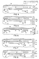
- FIGS. 4-8 The operation of the wafer transport system 18 is summarized by the sequence depicted schematically in FIGS. 4-8.
- the external blade 24 (with the wafer 15 to be processed supported thereon) is inserted via opening 56 into chamber 13 to a position over the susceptor 16.
- One example of a suitable blade 24 and associated robot wafer handling system (and door 25, FIG. 6) is described in European patent application No. (31501000/EA2799), entitled “Multiple Chamber Integrated Process System", which application is hereby incorporated by reference in its entirety.
- the wafer fingers 20-20 are positioned between the susceptor 16 and the blade 24.
- the wafer elevator mechanism 44 raises the wafer-support fingers 20-20 above the blade 24 to pick up the wafer 15.
- the blade 24 is then withdrawn from the chamber 13.
- a pneumatic cylinder closes door 25 over the blade access slot 56 to seal chamber 13.
- the susceptor elevator mechanism 46 is actuated to raise the susceptor-support fingers 22 and susceptor 16 so that the susceptor 16 lifts the wafer 15 from the fingers 20-20 into position for processing in the area 14 immediately adjacent the gas distribution manifold 26.
- the spacing, d, between the wafer 15 and manifold 26 is readily selected by adjusting the travel of the elevator 46.
- the susceptor fingers 22 and elevator mounting 46 maintains the horizontal orientation of the susceptor 16 and wafer 15 and parallelism between the wafer 15 and manifold 26 independent of the spacing, d.
- the susceptor elevator mechanism 46 lowers the susceptor fingers 22 and the susceptor 16 to deposit the wafer 15 on the wafer support fingers 20-20.
- the door 25 is then opened and blade 24 is again inserted into the chamber 13.
- elevator mechanism 44 lowers the wafer-support fingers 20-20 to deposit the wafer 15 on the blade 24.
- the blade is retracted, leaving the fingers 20 and 22 in the position shown in FIG. 4 preparatory to another wafer insertion, processing and withdrawal cycle.
- the radiant heating system shown in FIGS. 2 and 9 provides a reliable, efficient and inexpensive means for heating the circular susceptor 16 and wafer 15 (e.g., silicon) in a manner that provides uniform wafer temperature, accurate absolute wafer temperature and rapid thermal response at low temperatures, preferably ⁇ 600°C.
- a number of requirements must be met.
- achieving uniform wafer temperature requires compensating the radiation losses at the edge of the wafer.
- high efficiency at low wafer temperatures ( ⁇ 600°C) requires a high emissivity, high thermal conductivity susceptor 16 because silicon wafers have low emissivity at low temperatures in the near-infrared spectrum.
- near-infrared radiation is used to obtain fast heating response and for transmission through the inexpensive materials such as quartz window 70.
- the circular thin susceptor 16 is low thermal capacitance for fast heating and cooling response.
- the heating system 30 preferably comprises an annular array of small, inexpensive, single-ended vertically oriented lamps 58-58 which provide radiation in the near-infrared portion of the electromagnetic spectrum.
- the lamps 58-58 are mounted within an annular circular reflector module 60, preferably of aluminum.
- the module base 60 is formed from a block of aluminum, and has a polished annular reflecting channel 62 machined therein.
- the channel 62 has an arcuate, generally semi-circular reflecting base 64.
- the module 60 and lamps 58-58 are cooled by an annular cooling passage 66 that is formed within the collimating annular reflector 62. Connections are provided for the inlet and outlet of cooling liquid which, typically, is chilled water from a pressurized supply. Power is supplied to the lamp sockets 63 and associated lamps 58 by an electrical supply cable 68, typically from a variable power supply which automatically varies the lamp power based upon a predetermined program setting that is adapted to the requirements of the particular deposition process.
- the annularly-collimated light from the vertical oriented lamps 58-58 is admitted into the chamber via a quartz window 70. Quartz is transparent to near-IR radiation.
- the transparent quartz window 70 is mounted to the housing 13 at the bottom of the process chamber 13 using annular seals 72-72 to provide a vacuum-tight interface between the window 70 and the housing.
- This mounting arrangement positions the radiant energy heating source 30 outside the chamber 13 at atmospheric pressure and isolates the vacuum of the processing chamber and the particulate-sensitive processing therein from the lamps.
- a bracket 74 can be joined to the lamp mounting base 60 and pivotally mounted by pivot pin 76 to a mating bracket 78, which is joined to the housing 12. (Alternatively, the lamp module can be bolted in place).
- the lamp assembly is readily accessible for maintenance, lamp replacement, etc., by simply disengaging a clamp 79 to allow the assembly to pivot downwardly about pin 76.
- the lamps 58-58 are small single-ended commercially available quartz-tungsten-halogen lamps which provide the required near-infrared radiation.
- One suitable lamp is the Ansi type "FEL" supplied by Sylvania, G.E., Ushio or Phillips.
- FEL Ansi type
- fourteen 0.5 to 1 kilowatt quartz-tungsten-halogen lamps that provide a wavelength of about 0.9 to 1.5 micron provide an annularly-collimated power density of up to about 94 W/cm2 at the top of the lamp module.
- the maximum power density at the susceptor (substantially directed to the outer ⁇ 1.5 in. radius of a 6 in. diameter susceptor) is ⁇ 17 W/cm2 taking all efficiency into account ( ⁇ 15-16% efficiency).
- lamps concentrating their radiation in the range of about 0.7 to 2.5 microns wavelength would be particularly useful.
- the aluminum base 60 and concave-bottom, annular groove 62 provide a high collection-efficiency collimating reflector which directs a higher radiation power density at the susceptor edge than at the middle. This non-uniform, concentrated radiation heats the susceptor wafer circumferentially, which compensates the wafer edge heat losses and, thus, provides uniform wafer temperature over a wide range of chamber gas pressures and wafer temperatures.
- the desired uniform radiant wafer heating is provided by small, inexpensive lamps mounted in a compact simple aluminum module 60 that is easily cooled and maintained at a low temperature, and does not require plating.
- the use of the near-IR lamps and a thin, low mass, low thermal capacity, high emissivity susceptor of material such as graphite provides maximum efficiency, fast thermal response, excellent temperature uniformity and transmission through the quartz window 70.
- Other susceptor materials include anodized aluminum, graphite coated with layers such as aluminum oxide (Al2O3), or silicon carbide, or a composite ceramic coated with Al2O3 or SiC or other materials.
- interchangeable modules 60 having channels of different heights or diameters can be used to accommodate different susceptor and wafer diameters.
- a present version of the reactor is designed for 5-6 in. wafers.
- different lamp modules can be provided for smaller or larger diameter wafers by changing the module height and/or the radius of the module and the filament circle.
- the heating system 30 may employ a controller (not shown) such as a closed loop temperature control system using phase angle power control to provide rapid thermal response and rapid wafer temperature stability.
- the simplicity, low mass and high performance characteristics of the heating system 30 are in contrast to prior wafer heating approaches which typically use a rectangular array of double-ended quartz-tungsten-halogen lamps.
- Conventional radiation heating practice has been to use a more massive susceptor and, if excellent temperature uniformity is required, to merely block radiation from the wafer center, thus sacrificing efficiency, rather than redirecting radiation.
- the advantages of the radiant heating system 30 over the conventional practices include in addition to the aforementioned uniform wafer temperature and much faster response time (both heating and cooling), smaller, less bulky more easily maintained equipment of higher reliability (long lamp lifetime); more efficient operation; and lower cost.
- the gas distribution system 32 is structured to provide a unique combination of at least four structural features.
- the gas manifold 26 is one-half (the powered half) of an electrode pair.
- the powered manifold 26 provides high power.
- the gas manifold 26 and other gas distribution surfaces are temperature controlled, which contributes to uniform deposition on the wafer 15 and prevents gas decomposition, deposition or condensation within the gas distribution system upstream from the plasma processing area 14 despite the use of reactant gases such as TEOS which condenses at ⁇ 35°C and decomposes or reacts with ozone at ⁇ 75°C.
- the external manifold temperature is controlled, e.g., to >100°C, to prevent the deposition of flaky, particulate-causing deposits.
- the gas manifold 26 and gas distribution system 32 provide a clean, uniform deposition process.
- the incorporated circumferential purging gas flow prevents deposition outside of the gas distribution area, i.e., outside the wafer on the internal chamber surfaces and gas distribution system surfaces.
- gas distribution system 32 The above features of gas distribution system 32 are depicted most clearly in the FIG. 2 vertical section view and the FIG. 10 enlarged vertical section view.
- the gas manifold 26 and associated distribution system are part of the housing cover 80, which is pivotably mounted to the housing 12 by pivot means (not shown) to facilitate access; to the interior of the housing, including chamber 13, plasma process chamber 14, and associated internal components of the wafer and susceptor elevator mechanisms (44,46).
- the process gas flow from the feed-through 36 is directed into the cover 80 by inlet bore 88 which communicates with, that is, feeds into, gas manifold chamber 90 formed by the apertured manifold face plate 92.
- a uniquely designed baffle plate 94 is mounted within the gas manifold chamber 90 by means such as standoffs (not shown) to route the process gas around the outside of the edge of the baffle 94 and then radially inwardly along the bottom of the baffle and out of the apertures 96-96 in the manifold plate into the plasma processing region 14 above wafer 15.
- the cover 80 including the manifold 26 thereof, is heated (or cooled) by an internal flow of fluid or liquid such as de-ionized water along internal path 81 defined by inlet channel 82, annular channel 84 and outlet channel 86.
- this flow keeps the face plate 92 within the range 100°C - 200°C, in order to ensure that any deposition on the face of the gas manifold which is exposed to the plasma is a hard film. A poor film formed on this surface can create particulates and this must be avoided.
- the flow preferably holds baffle 94 within the range, most preferably within 35°C-65°C, to prevent internal deposition or condensation of low vapor pressure process gases such as TEOS and to prevent decomposition and reactions of gases such as TEOS and ozone.
- TEOS low vapor pressure process gases
- TEOS decomposition and reactions of gases
- ozone ozone
- De-ionized water is used because the manifold 26 is the RF powered cathode and de-ionized water is a non-conductor.
- the inlet temperature of the water is selected as required for a particular deposition process and its associated gas chemistry and/or parameters in order to maintain both the internal surfaces and the external surfaces of the gas box 90 at desired temperatures.
- the process gas flow is along path 91 defined through inlet bore 88, into manifold chamber 90, radially outwardly to the edge of baffle 94 and around the baffle periphery to the bottom thereof, then radially inwardly between the baffle 94 and the manifold plate 96 and out holes 96-96 into the plasma processing region 14 above the wafer 15.
- the flow path of the deposition gas emerging from holes 96-96 is generally radially outwardly across the wafer.
- the small volume of the vacuum process chamber 14 and the high useful chamber pressure range of about 0.5 torr to near-atmospheric pressure also contribute to the tendency to provide a uniform flow radially outward from the center of the wafer 15 with uniform deposition on the wafer and purging without deposition other than on the wafer.
- the manifold holes 96-96 are designed to promote this uniformity of deposition.
- the holes (as well as the manifold temperature, discussed above) are also designed to avoid the formation of deposits on the manifold outer (bottom) surface 97 and, in particular, to prevent the deposition of soft deposits on surface 97 which could flake off and drop onto the wafer during and after processing.
- the hole array is one of generally concentric rings of holes 96-96. The distances between adjacent rings (ring-to-ring spacings) are approximately equal, and the hole-to-hole spacing within each ring is approximately equal.
- the patterns are angularly staggered so that no more than two adjacent holes (or some other selected number) are aligned radially. That is, the holes in the gas distribution plate 92 are equally spaced on circles so the hole locations do not form radial straight lines, thereby substantially decreasing deposition on the gas distribution plate itself and enabling uniform gas flow and deposition on the wafer.
- the hole length through the manifold 92 i.e., the thickness of the manifold plate 92, and the transverse hole diameter are also selected to promote uniform deposition. Increasing/decreasing the hole length has the effect of decreasing the deposition thickness inside-out/outside-in, as does increasing/decreasing the hole diameter.
- approximately 3400 holes 96-96 are used.
- the hole length is 0.100 to 01.150 in.
- the hole diameter is 0.028 to 0.035 in.
- the radially asymmetric holes are located on approximately 0.090 in. centers.
- These dimensions and the associated configuration provide a uniform flow pattern and substantially decrease deposition on the manifold plate 92.
- the present ⁇ 6 in. manifold diameter will accommodate wafer diameters as large as ⁇ 6 in. Larger wafers can be processed by changing to a larger manifold 26, susceptor 16, larger diameter susceptor 16 and wafer support finger arrays, and by altering the lamp module 30 as described previously.
- a first, upper purge gas flow path is provided in cover 80 and manifold 26. That is, purge gas flow from the RF/gas feed-through 36 is routed into inlet bore 98 in cover 80 (arrow 93) which feeds into radial channels or grooves 100 that in turn feed into an annular groove 102 formed in the cover concentric with and just above and outside the manifold chamber 90 (arrow 95).
- a ring flow turner 104 is mounted concentrically within manifold plate rim 105 and forms a peripheral channel 106 at the inside of the manifold rim that connects the annular channel 102 to the three outer rows of apertures 108 in the manifold plate 92.
- the purge holes 108-108 are arranged similarly to the process gas holes 106-106 in generally concentric rings that are spaced at approximately equal ring-to-ring distances.
- the within-ring hole spacing is selected so that the locations of the purge holes 108-108 form staggered radial lines, i.e., so that no two adjacent purge holes are along the radial line.
- the gas is distributed from about 600 holes and the following purge hole dimensions are used: between-ring spacing 0.090 in.; hole diameter 0.025 in.; and hole length 0.040 in.
- a second, lower purge flow path 101, 103, 105 is provided via inlet bore 110, formed in the side of the housing 12, which connects or feeds into an annular channel 112 formed generally concentrically about the lower section of the process chamber 13 just above the quartz window 70.
- the channel 112 has holes that are spaced about the lower region of the chamber 13 or equivalent yielding feature to feed the lower purge gas uniformly across the quartz window 70 (see arrows 103), around the lower edge of the wafer 15 (arrows 105) and across horizontal quartz cover plate 114, which surrounds the chamber 13 just below the wafer processing chamber 14.
- the plate 114 contains an annular pattern of holes 116 therein which are aligned with an annular gas outlet channel 118.
- This channel is connected via outlet bore 121 to a conventional vacuum pumping system (not shown), which establishes the vacuum within the chamber and exhausts the spent gases and entrained gas products from the chamber.
- the upper purge gas flow is through inlet 98 (arrow 93), channels 100, 102 and 106 (arrow 95), then out purge ring apertures 108-108 (arrow 93) at the outer upper edge of the process-positioned wafer 15.
- the lower purge gas flow is through inlet 110 (arrow 101) and annular ring 112 across the quartz window 70, sweeping the window clean (arrow 103), then upwardly toward the lower peripheral bottom edge of the wafer 15 (arrow 105).
- the upper and lower gas purge flows 97 and 105 merge at the wafer's edge and flow outwardly as indicated by arrow 107 across the plate 114 and through the holes 116 therein into the annular exhaust channel 118 and out of the chamber along path 109 (FIG. 2).
- This upper and lower, merging flow pattern not only keeps the quartz window 70 clean, but also sweeps spent deposition gases, entrained particulates, etc., out of the chamber 13.
- the combination of the dual, upper and lower purge flows which are conformed to the inner quartz window chamber surfaces and to the circumferential wafer edge and the very high chamber pressures (unusually high for PECVD) provide a very effective purge and prevent deposition external to the wafer.
- uniform gas flow is provided across the wafer 15 by the multiplicity of holes 116-116, illustratively five in number, which are formed in the distributor plate 114 peripherally around the wafer 15. These holes 116 communicate into the larger semi-circular exhaust channel 118 which, in turn, is connected to the vacuum exhaust pumping system via the single outlet connection 121.
- the channel 118 has large conductance relative to the holes 116-116 because of its relatively very large volume, which provides uniform pumping at all points radially from the wafer, with the simplicity of a single point pump connection.
- this uniform radial pumping provides uniform gas flow across the wafer 15 at all pressures and, thus, uniform deposition even at very high chamber pressures such as 200 torr and above.
- manifold 26 is usable as an electrode for a uniform glow discharge plasma at unusually high pressures, which enables both the very high deposition rate and the effective purge flow.
- the advantages of using the gas box 26 as the powered RF electrode include the wafer residing on the grounded counter electrode, which makes possible a high degree of plasma confinement that would not be achievable if the RF energy was applied to the wafer and the gas box was grounded. Additionally, the hardware is mechanically and electrically simpler since electrical isolation between wafer/susceptor and chamber is not required (or permitted). Temperature measurement and control of the susceptor/wafer in the presence of high frequency electric and magnetic fields is greatly simplified with the susceptor grounded.
- Our combination RF/gas feed-through 36 (FIG. 12) is designed to apply RF power to the gas box 26, that is, to use the gas box as the powered RF electrode, without breakdown of the process gas and without deposition within the gas distribution system.
- the RF/gas feed-through 36 is of a compact, low profile design, despite our design objective that the high RF potential be applied parallel to the gas flow path to yield a constant voltage gradient over a distance to eliminate the high local electric field which causes electrical breakdown.
- the first approach flows the gas within an insulating tube between surfaces that are at a high electric potential difference.
- a second approach flows the process gas through an insulator between the surfaces of high electric potential difference at sufficiently high gas pressure so that electrical breakdown does not occur.
- the first approach is not compact and does not work at high frequencies, where electrical breakdown is more efficient (see, e.g., curve 201 and 200, FIG. 14). Also, this first approach is not capable of operation where there is a small p ⁇ d (pressure ⁇ distance) product.
- the second approach is more compact than the first, and less susceptible to electrical breakdown at high frequencies, but is also subject to electrical breakdown where there is a small pressure ⁇ distance product.
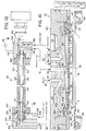
- the feed-through 36 comprises an inlet end connector or manifold 120, an outlet end connector or manifold 122 and an intermediate gas feed structure 124 comprising a quartz tube 126 and an elongated insulating transition housing 128.
- the block 128 is mounted to and between the end connectors 120 and 122 using O-ring seals 130-130 to provide vacuum-tight mounting.
- the internal bore 127 of the quartz tube 126 communicates with gas inlet bore 134 in the inlet end connector and gas outlet bore 136 in the outlet end connector.
- Process gases and purge gas under pressure from sources such as an ozone generator, a liquid-TEOS vaporizer, and conventional pressurized gas tanks or bottles are routed through conventional valves or an automatic flow control system for controlled flow rate application to the inlet manifold 120.
- process gas is routed through the feed-through device 36 via the inlet bore 134 and through the quartz tube 126 and out the outlet bore 136 and into the mating inlet bore 88 in the gas distribution head 32.
- the feed-through is shown enlarged in FIG. 12 to facilitate illustration.
- the actual feed-through 36 is of a size so that the gas outlets 136 and 146 are aligned with the mating channels or bores 88 and 98 in the reactor cover 80.
- the purge gases are routed through the feed-through co-axially with the process gas flow path so that if there is a leak along the process gas path 131-133-135, the process gas is harmlessly transported into the process chamber 14 along with the purge gas and, thus, does not escape into the ambient.
- the incoming purge gas is applied to inlet bore 138 in the inlet end connector 120.
- Bore 138 communicates with an annular channel 139 formed in the spool-shaped fitting 140 which is mounted near the inlet end of the quartz tube 126.
- This spool fitting 140 is sealed at the outer end thereof by cylindrical flange fitting 142 and O-ring seal 144.
- the annular channel 139 communicates via holes (not shown) with the annular passage 147 between the tube 126 and concentric block passage 147 between the tube 126 and concentric block 128.
- the passageway 147 feeds similarly into annular chamber 139 in fitting 140 at the outlet end of the tube 126.
- the tube 126 is mounted and sealed at the outlet in the same way described above relative to its inlet end.
- chamber 139 feeds into the outlet bore 136.
- This arrangement provides an isolated purge gas flow path through the feed-through 36, as indicated by arrows 148-156.
- the co-axial gas feed apparatus described above provides a dual barrier which prevents the leakage of potentially toxic process gases into the atmosphere. That is, the path to the ambient between mating surfaces is barred by the two sets of O-ring seals 130 and 144. These seals are positioned in series along the potential path to the ambient. Also, as mentioned, in the event of internal system leaks such as a leak in the quartz tube 126, the purge gas flow carries the process gas into the process chamber 14, where both are exhausted by the chamber vacuum system. In addition, the process and purge gases are routed entirely through the chamber components, i.e., through substantial blocks/bodies such as the aluminum connectors 120 and 122 and the insulator block 128. Consequently, external, typically flexible, gas tubing is eliminated at the reactor. The very solid, secure routing fixtures, the dual seal barriers, and the co-axial gas flow in which the purge gas flow surrounds the process gas flow, provide a safe, secure process gas flow path in the reactor and feed-through device.
- the inlet end connector 120 is connected to ground.
- the outlet end connector 122 is connected to the RF power supply 128 and connects the RF energy to the cover 80 and manifold plate 92.
- a constant electric potential gradient is provided along the column of process gas flow between the grounded connector 120 and the driven connector 122 by providing one of three types of constant voltage gradient elements along the surface of the quartz insulating tube 26: a radio frequency coil which provides resistive, inductive, or capacitive (effective) impedance; a resistive film; or a resistive sleeve.
- the RF coil 160 is a wire coil that is wound around the quartz gas tube 26 between the ends thereof and the high voltage which is applied across the tube length.
- the wire coil 160 is of No. 24 to No. 26 AWG aluminum wire.
- the desired electrical impedance at the frequency of operation is obtained by selecting the wire material, diameter, number of turns per unit length, length and the winding technique.
- This A.C. impedance can be selected to have a net inductive/resistive impedance or a net capacitive/resistive impedance or to be purely resistive (resonant).
- the A.C. and D.C. resistance can be selected (using wire diameter, length, and material).
- a typical application has a high inductive reactance but is a D.C. short.
- typical values for the inductance of an RF coil-type feed-through are approximately 10-15 microHenries.
- a resistance of 100 to 500 Kohms is typical.
- a resistive film 162 of material of controlled electrical resistivity and thickness such as Acheson "Aerodag G” (a colloidal suspension of micron size graphite particles in an isopropyl alcohol dispersing medium), is coated on the outside of the quartz tube 126 to provide the desired resistive impedance and allow broad band (frequency) operation.
- Acheson "Aerodag G” a colloidal suspension of micron size graphite particles in an isopropyl alcohol dispersing medium
- the third alternative shown in FIG. 13C uses a solid resistive sleeve 164 of a material such as a composite ceramic of controlled electrical resistivity, to provide the desired electrical resistive impedance and broad band frequency operation.
- a variant of the solid resistive sleeve 164 uses a sleeve of material which is ferromagnetic with very high permeability at the frequency of interest ⁇ and has controlled electrical resistivity. Operation is the same as for the resistive sleeve 164, with this added advantage. Should breakdown occur under severe conditions, the presence of magnetic material and initially high current and resulting high magnetic field produces a very large inductive reactance to charge flux (current), which very quickly reduces then extinguishes electrical conduction in the process gas.
- FIG. 14 illustrates representative bench test data for a quartz tube without a constant voltage gradient device of voltage breakdown in kilovolts as a function of pressure in torr at both low (100 kHz) and high (13.56 MHz) radio frequencies. As indicated, for the pressure range of 5-20 torr, the breakdown range was 3 to 7 kV for the low radio frequency and approximately 2 to 5 kV for the high radio frequency.
- FIG. 15 illustrates bench test data of breakdown voltage as a function of pressure for Tube A, a tube of length 10.5 cm and diameter 0.6 cm without a constant voltage gradient device, and Tube B, the same tube with a constant voltage gradient device of the wire coil type 160, consisting of 160 turns of ⁇ 26 AWG wire.
- Tube C was the same as tube B, except for having a greater length, 13.4 cm.
- This illustrates that the RF/gas feed-through 36 is very effective in preventing breakdown and subsequent deposition of process gases under actual reactor operating conditions.
- the reactor system 10 will be used at pressures of up to 200 torr and above, at which values the breakdown voltages will be much higher than those depicted in FIG. 14.
- the anti-electrical breakdown gas feed-through 36 of the present invention provides a constant voltage gradient along the process gas flow column, without charge build-up.
- the feed-through 36 is designed to incorporate resistive, inductive or capacitive electrical impedance between the high potential difference ground and driven surfaces. The choice of impedance depends upon the electrical requirements of the system, i.e., low frequency, high frequency, wide band, d.c. operation, etc. This constant electrical potential gradient effectively prevents premature breakdown and deposition within the gas distribution system 32 and feed-through 36 at high or low radio frequencies.
- the structure of the feed-through 36 including the co-axial gas feed is highly resistant to process gas leaks and purges any process gas leaks into the system exhaust.
- temperature controlled water can be flowed through channels (not shown) in the feed-through device 36 isolated from process and purge channels to (heat or cool) control the temperature of the gas in the feed-through.
- gases such as ozone or TEOS
- Our reactor uses a tailored non-uniform near-IR radiant heating pattern and a thin, low mass high emissivity susceptor to provide thermal efficiency, fast thermal response (heating and cooling), excellent temperature uniformity despite the inherent non-uniform heat losses of thin circular wafers, and good transmission through a chamber window of quartz or the like (which permits external mounting of the radiant heating module).
- the RF powered gas manifold 26 provides the necessary high power to enable confinement of the plasma.
- the uniform gas inlet flow pattern provided by the gas manifold and radial exhaust pumping provide uniform gas inlet and exhaust (purge) pumping and uniform radially gas flow across the wafer, enabling uniform processing (deposition/etching) over a wide pressure regime including very high pressures.
- the radial pumping and high pressure capability provide confinement of the plasma/reactant species to the wafer and; in enabling effective purging, prevent deposition within the chamber except on the wafer.
- the precisely temperature-controlled internal and external surfaces of the gas manifold prevent decomposition, reactions, condensation, etc., within the gas box and eliminate undesirable particulate-generating deposits on the external gas box surfaces.
- temperature controlled water is circulated within the gas box to maintain the temperature between about 35°C-75°C to prevent internal deposition or condensation of TEOS below about 35°C and to prevent internal decomposition of or reaction between ozone and TEOS above about 70°C, and to maintain the external face of the gas manifold greater than about 100°C to prevent flaky external deposits.
- the gas feed-through provides the enables the application of high voltage RF power to the gas box, as well as the application of purge gas and process gas to the gas box, without gas breakdown.
- a one-axis robot susceptor/wafer support and transport system is adapted to load and unload wafers at a selected position within the chamber onto and from an external robot blade.
- This transport system provides variable parallel close-spacing between the susceptor/wafer and the overlying gas manifold and provides variable spacing by simply selecting the vertical travel of the associated susceptor support fingers and susceptor elevator mechanism.
- the parallelism increases plasma stability and uniformity by eliminating the tendency to run to one side or the other and, thus, enables uniform processing (deposition and etching).
- the variable close spacing of the distance, d, between the outer face of the gas manifold and the wafer surface facilitate the implementation of different types of process.
- the spacing can be set at a very small variable dimension such as, for example, one centimeter, 0.5 centimeter and even smaller, to enable confinement of the plasma and/or gaseous reactants between the gas distributor and the wafer. This confinement increases the reaction efficiency and increases the rate of the reaction (deposition or etching) and helps prevent deposition everywhere except on the wafer, and even at very high pressures.
- High pressure capability results from a number of the above-summarized factors including uniform radial pumping, the uniform gas flow provided by the gas manifold, the confinement provided by the variable close spacing between the electrodes and the application of high power density RF power to the gas manifold.
- Temperature control of the gas box external surface to >100°C is important to prevent the deposition of porous particulate causing films.
- High pressure operation increases ion scattering, which decreases bombardment of and damage to the wafer and enhances step coverage. This, because high pressure operation dilutes the concentration of the gas molecules to the point where they do not react at a sufficient rate to cause particles/unwanted deposition on surfaces.
- the high pressure capability and associated decreased bombardment enables one to decrease the bombardment level for a given power/voltage and reaction rate or, alternatively, to use higher power/voltage to obtain a higher reaction rate for a given bombardment level.
- Uniform flow distribution is also critical, particularly at the close spacing of less than one centimeter used in our reactor, because it confines the plasma and thus enhances clean operation.
- the ability to adjust the electrode spacing with parallelism permits the use of the close spacing with the plasma stability necessary for deposition.
- variable large spacing in combination with the high pressure capability permits effective etchback.
- the variable spacing between electrodes is very important because it would be impossible to optimize the etch and other processes without varying the electrode spacing used for deposition. For example, a typical spacing of ⁇ 1 cm is used for thermal CVD and PECVD while the etchback requires a spacing of ⁇ 0.4 in. or 1 cm.
- variable spacing in combination with variable pressure permits effective reactor self-cleaning.
- the required spacing, d, ⁇ 0.4 in. or 1 cm. is larger than that required for, e.g., thermal CVD and PECVD.
- the relatively larger spacing and wide pressure regime permits the plasma to diffuse within the reactor (rather than being confined as required for the deposition processes) and clean the entire reactor.
- a typical self-cleaning sequence uses RF power of 500 watts, gas NF3 or other fluorine containing chemistry at flow rates typically of 0.1 slm, pressure of 0.5 torr, and d ⁇ 0.4 in., and has provided ebb rates of ⁇ 0.5 micron/sum.
- the high pressure capability combined with 0.2 in. spacing as well as the ability to apply RF power to the gas box at high power levels permits sputtering of materials such as oxide or other drelectrics using gas chemistry such as argon or other heavy molecule gas chemistry such as SiCl4.
- a typical sputtering process involves application of RF power of 700 watts, gas flow rates 0.1 slm, pressure of 10 mt. electrode spacing, d, of 0.2 in. to 0.5 in.
- the processing steps and multiple step processing sequences described here were performed in the reactor 10.
- the ability to perform multiple step processing using temperature sensitive gases such as ozone and TEOS and different steps such as CVD, PECVD, etching, and self-cleaning in-situ qualifies the reactor 10 as being uniquely preferred.
- temperature sensitive gases such as ozone and TEOS
- different steps such as CVD, PECVD, etching, and self-cleaning in-situ qualifies the reactor 10 as being uniquely preferred.
- the process disclosure here will permit those of usual skill in the art to practice the process sequences albeit in single process, dedicated reactors and to adapt such reactors, e.g, to the use of the process.
- the thermal chemical vapor deposition of highly conformal silicon dioxide is an improvement of methods which use the pyrolysis of TEOS and oxygen.
- the present thermal CVD invention is based in part upon the discovery that improved highly conformal ( ⁇ 100%) silicon dioxide coatings are formed by the thermal chemical vapor deposition of the reactants TEOS and ozone at relatively low temperatures, using lamp radiant heating to provide a wafer temperature of about 200°C - 500°C, and high pressures.
- the ozone lowers the activation energy of the reaction kinetics and forms silicon dioxide with the TEOS at the relatively low temperatures of about 200°C to 500°C.
- a commercially available high pressure, corona discharge ozone generator is used to supply a mixture of (4-8) weight percent ozone in oxygen to the gas distributor.
- Helium carrier gas is bubbled through liquid TEOS to vaporize the TEOS and supply the diluted gaseous TEOS in the He carrier to the gas distributor.
- the thermal chemical vapor deposition process uses the reactants ozone (O3), oxygen and tetraethylorthosilicate (TEOS) at a low temperature within the range of about 200°C-500°C and at a high pressure within the range of about 10-200 torr and, preferably about 40-120 torr, to deposit a highly conformal silicon dioxide coating that fills in the voids, cusps and other topographical irregularities and thereby provide a substantially planar surface.
- O3 ozone
- TEOS tetraethylorthosilicate
- the ozone is applied at a flow rate of 2 to 3 slm
- the helium carrier gas flow rate is 50 sccm to 1.5 slm
- the chamber pressure is 40 to 120 torr
- the wafer temperature is 375°C ⁇ 20°C, thereby providing a highly conformal undoped silicon dioxide coating at a deposition rate of 3,000 Angstroms/min.
- the gas distribution manifold (gas distributor 26) of the reactor 10 is controlled by de-ionized water of temperature 20-50°C circulating in passages therein to maintain the internal surface of the gas distributor 26 within the narrow range of about 35°C-75°C, i.e., at a temperature of less than about 75°C to prevent decomposition of the TEOS and reaction between the TEOS and ozone and above 35°C to prevent condensation of the TEOS inside the gas distributor.
- the distance, d, from the temperature-controlled gas distributor to the surface of the substrate is preferably approximately one centimeter or less. This distance of one centimeter or less confines the plasma or gaseous reactants between the gas distribution 26 and the wafer 15. This increases the reaction efficiency, and increases the rate of the reaction (deposition) and helps to prevent deposition everywhere except on the wafer.
- the thermal CVD process of the present invention uses unusually high deposition chamber pressures: pressures of preferably at least ⁇ 10 torr and of about 20-200 torr are utilized. Even the lower portion of this range is over 20 times greater than the total pressure normally utilized in processes utilizing TEOS.
- the high pressure increases the density of available reactive species and, thus, provides a high deposition rate.
- the use of high pressure enables an effective purge.
- the high purge flow rate improves the ability to remove waste gases, entrained particulates, etc., without unwanted deposition on the chamber surfaces.
- the above-described bottom purge flow sweeps radially outwardly across the bottom side of the susceptor wafer.
- the bottom flow is joined by an upper purge flow that is directed downwardly at the wafer's periphery.
- the combined streams flow radially outwardly from the periphery of the wafer, and cause the deposition gas to flow radially uniformly outwardly, then through the exhaust system of the chamber at very high flow rates.
- useful top purge gas flow rate (preferably nitrogen) may be from 1 slm to 10 slm and the bottom purge gas flow rate (again, nitrogen) may be 1 slm to 20 slm.
- the above-described gas flow, chamber pressure, and resulting chamber temperature have provided a silicon dioxide deposition rate of about 500 Angstroms/min. to 4,000 Angstroms/min.
- the deposition rate peaks at about 375°C ⁇ 20°C.
- the decreased deposition above and below the peak is a consequence of unfavorable reaction kinetics at the surface of the substrate.
- the peak temperature is also close to the maximum processing temperature of about 400°C for aluminum-containing multiple conductor structures. Above ⁇ 400°C, hillocks form in aluminum. Above ⁇ 500°C, aluminum softens.
- the deposition rate saturates at 3,000 Angstroms/min. at a chamber pressure of 80 torr, and wafer surface temperature of 375°C (using a TEOS temperature of 35°C), with very little increase at higher pressures. Decreasing the temperature to 200-375°C at 80 torr decreases the deposition rate to 1,000-3,000 Angstroms/min., respectively. At 20 torr, temperatures of 200-375°C provide a deposition rate of 500-1000 Angstroms/min. Above pressures of about 120 torr, gas phase reactions increase particulates. This can be controlled by decreasing the wafer temperature or increasing the diluent flow rate, but these steps decrease the deposition rate.
- the resulting films have been characterized as having improved physical and electrical properties such as cracking resistance, density, refractive index, shrinkage, rate of etching, breakdown voltage, flat band voltage, mobile ion contamination, pin hole density and silicon oxide purities, the crucial aspect is the excellent ⁇ 100% conformal coverage over vertical and horizontal surfaces of steps and over other surface irregularities. Consequently ⁇ problems such as overhang, cusps and voids are much less severe, thereby minimizing or even eliminating the amount of follow-up processing which must be done to remedy such problems and to achieve planarization.
- the conformal oxide could be doped to a low level of, e.g., 1 weight percent to 10 weight percent of phosphorus and/or boron by incorporating reactants such as TMP (tetramethylphosphite) and/or TMB (tetramethylborate).
- reactants such as TMP (tetramethylphosphite) and/or TMB (tetramethylborate).
- TMP tetramethylphosphite
- TMB tetramethylborate
- the process of the present invention is an improvement of conventional methods for planarizing silicon dioxides such as, for example, conventional methods using spin-on glass and polyimide deposition with etch-back.
- Another aspect of the present invention is the use of the above-described thermal CVD silicon dioxide deposition process to substantially planarize a dielectric layer, followed by the use of an isotropic wet or dry etch, preferably at a high etch rate, to complete the planarization process.
- the combination of the above-described low temperature, thermal CVD, conformal oxide deposition process in conjunction with various wet or dry isotropic etch steps provides an unexpectedly conformal planarized dielectric layer which serves well in the small geometry, multi-level metallization structures that are currently being developed and will be developed in the future. Described below is a presently preferred dry isotropic etch process which can be performed in-situ, in the same, referenced multi-step chamber.
- the present invention is embodied in a three-step process which, first, forms a layer of silicon dioxide, preferably at a high deposition rate; the above-described ozone and TEOS-based thermal CVD conformal oxide deposition process is used as the second step to form a highly conformal oxide coating; then, in the third step, a preferably high rate isotropic etch is applied to quickly complete the planarization process.
- the above-described thermal CVD, conformal oxide deposition process is used in a three-step high deposition rate, high throughput planarization process in-situ in the referenced multiple process CVD/PECVD deposition chamber.
- the planarization process can be applied over existing dielectric layers or can be used alone to form a planar dielectric.
- the preferred first step is a PECVD oxide deposition.
- the PECVD oxide deposition process uses a plasma formed from TEOS, oxygen, and a carrier gas with or without a diluent such as helium. This process uses a deposition chamber pressure of from about 1 torr to about 50 torr; an oxygen rate of from about 100 sccm to 1,000 sccm, an inert carrier gas (helium) flow rate of from 100 to 1,500 sccm, a total gas flow rate (not including the purge gases) of 200 sccm to 2.5 liters per minute, and RF power to the ⁇ 6 in. diameter gas distributor cathode of about 200 - 400 watts.
- Power density at the gas distributor/cathode 26 is about 1 watt/cm2 based on calculations for a quasi-parallel plate configuration. Radiant energy is directed to the susceptor from below by the annular array of vertical lamps to generate a deposition plasma and heat the wafer surface to a temperature of 300 to 500°C. Top (nitrogen plus helium mixture) and bottom (nitrogen only) purge gas flow rates of 1 to 15 slm and 1 to 20 slm, respectively, are used with respective preferred top and bottom purge gas flow rates of 2.5 slm and 10 slm. These parameters provide SiO2 deposition rates of about 5,000 Angstroms/min. to 10,000 Angstroms/min. Typically, 0.4 cm ⁇ d ⁇ 1 cm.
- Presently preferred operating parameters for the PECVD oxide deposition step for a 6 in. wafer are 600 sccm oxygen 900 sccm helium, 16,000 sccm total flow (including purge; 1,500 sccm excluding the purge), 10 ⁇ 2 torr pressure and 375°C ⁇ 20°C wafer temperature.
- the parameters provide SiO2 deposition rates of about 8,500 Angstroms/min. for a gas distributor-to-wafer surface distance, d ⁇ 0.4 cm.
- the above-described high pressure, PECVD oxide deposition process which is based upon TEOS gas chemistry and has essentially the same chamber requirements as the crucial conformal silicon dioxide deposition step, makes the use of the same chamber not only possible, but preferable.
- TEOS tetraethylorthosilicate
- This pyrolysis process may be utilized, with a silicon nitride, silane and ammonia plasma, or with an oxynitride, silane, ammonia and N2O plasma.
- Plasma-assisted chemical vapor depositions using TEOS at pressures below 1 Torr are also utilized, with variations including use of spin on glass, and polyimides.
- the present PECVD process provides methods for improving deposition rate, cracking resistance, physical and electrical properties of CVD-deposited silicon dioxide.
- the present invention also provides an improved method for depositing silicon dioxide whereby improved step coverage and lower stress of the deposited layer are obtained.
- the present PECVD process provides an improved method for the plasma-enhanced chemical vapor deposition of TEOS to obtain the above advantageous improvements whereby the preferred conditions of deposition are a higher than usual pressures (up to 50 Torr) and at temperatures of about 200 to 400°C.
- the usual conditions for the plasma-enhanced chemical vapor deposition using TEOS are at a total pressure range of up to about 1 Torr (including the carrier gas), of which the oxygen in the plasma is at a pressure of about 0.4 Torr.
- the substrate temperature usually gradually increases from about room temperature to about 400°C. See, for example, Mackens et.al., Thin Solid Films , 97:53-61 (1982).
- the deposited silicon dioxide coatings according to the present invention also have improved cracking resistance and have improved step coverage over silicon dioxide coatings deposited by other methods.
- the problem of step coverage deals with the creation of a mushroom-shaped deposited overhang at the corners of the step substrate. This overhang must be removed by subsequent processing, thus complicating the process.
- the problem of the overhang is much less severe, thereby minimizing or even eliminating the amount of processing to remedy this problem.
- the silicon dioxide coatings formed according to the present invention also exhibit lower stress and are characterized generally by indices of -IE9 (compression) to +IE9 (tension), with the preferred index being -IE8. Also, the coatings according to the present invention exhibit improved physical and electrical properties and that the density, refractive index, shrinkage parameters, rate of etching, breakdown voltages, flat band voltages, mobile ion contamination, pinhole densities and silicon oxide purity are improved.
- the operation at high pressures allows the plasma to be confined at the top of the substrate, thus making it less likely to contaminate the sides of the chamber and the surfaces on which deposits are not desired.
- the third step is a high rate isotropic etch process comprising the step of exposing the existing silicon dioxide surface to the plasma formed from fluorinate gas selected from CF4, NF3 and C2F6 in a doping gas such as helium to stabilize the plasma, in a chamber at a temperature in the range of about 100°C to 500°C and preferably 200°C to 400°C.
- a doping gas such as helium to stabilize the plasma
- the total gas chamber pressure for these gases will usefully be in the range of about 200 mt to 20 torr.
- the preferred range is 500 mt to 10 torr.
- the total gas flow rate of the plasma will be determinable by those skilled in the art.
- the preferred total gas flow rate is from about 170 sccm to 1.25 slm.
- the useful range for the NF3 (or C2F6) gas flow is from about 10 sccm to 500 sccm, with the preferred range being from about 70 to 200 sccm.
- the individual flow rate of the doping gas, usually helium, will be from about 10 sccm to 3.5 slm and, preferably, 100 sccm to 1 slm.
- RF power density of about 0.5 -1 watts/cm2 was used, along with radiant power from the lamp module to provide the substrate temperature of ⁇ 500°C and the preferred temperature of 200°C - 400°C.
- a distance d ⁇ 0.4 cm is used. Below 0.4 cm, plasma instability increases. Also, as d is increased above 1 cm, the etch may become too effective and etch other components.
- this isotropic etch process is also useful generally, for example, for forming metal contacts, it is particularly useful for providing profile control of SiO2 step-coverage layers, as described above,.
- this uniform high rate isotropic etch has the advantage of additionally planarizing the substantially planarized contour which results from the SiO2 deposition.
- This high rate isotropic etch step was done in-situ in the same reactor used for the two above-described silicon dioxide deposition steps.
- this preferred sequence provides an integrated in-situ three-step process for forming a planarized silicon dioxide layer even over non-planar layers incorporating small geometry steps, trenches, etc.
- the use of the high rate PECVD oxide deposition step and the high rate etching step the ability to use the same chamber for all three steps provides a fast, high throughput planarization process which is also less susceptible to contamination and wafer damage and other problems which result when a wafer is handled repeatedly and switched from one chamber to another.
- FIGS. 18 and 19 The use of the above-described three-step planarization process is shown schematically in FIGS. 18 and 19.
- the first step forms a relatively thick stepped layer 182 of silicon dioxide over the stepped topography 181 at a very high deposition rate.
- the second step is then used to form thereon conformal silicon dioxide layer 183, which is substantially planarized despite the underlying deep step 184.
- the third, isotropic etch step quickly etches away the upper surface 185 below the residual step topography 186, if any, in layer 183, thereby providing a smooth planar surface 187 for subsequent layers.
- the ozone- and TEOS-based thermal CVD step can be used in combination with other initial dielectric coatings and other isotropic etch steps.
- the ozone thermal CVD second step can be used to deposit a highly conformal silicon dioxide coating on silicon oxide or silicon nitride or silicon oxynitride or other dielectric layers formed by CVD or by other methods, and the resulting substantially planarized layer can be etched to a planar topography using other, preferably high rate, dry (e.g., plasma) or wet chemical isotropic etch methods.
- An isotropic chamber self-cleaning etch sequence has been done using fluorinated gas at a pressure of about 600 mT to 10 torr, high RF power density of 1 - 2 watts/cm2, distance, d ⁇ 1 cm and the other parameters, including the gas flow rates, described above for the isotropic etch process.
- This process has been used to clean the referenced multi-step CVD-PECVD reactor. After depositing an ⁇ 5 ⁇ thick silicon dioxide film on a wafer, the chamber can be cleaned in about one minute.
- the thermal CVD conformal-oxide deposition process using ozone, oxygen and TEOS can be used alone to planarize an existing dielectric which has been formed, for example, without perfect step coverage or with perfect step coverage on a non-perfect topography.
- the conformal oxide-forming thermal CVD step can be applied to existing dielectrics followed by an isotropic etch step to etch back any remaining non-planarities to a planar topography.
- the above-described high rate PECVD oxide step is applied followed by the conformal oxide-forming thermal CVD sequence.
- the high rate PECVD oxide deposition sequence is utilized followed by the conformal oxide-forming thermal CVD step followed by an isotropic etch step, preferably the above-described high rate plasma isotropic etch.
- the first two steps of the following sequence can be used to planarize the stepped topography followed by application of the high rate oxide deposition to build up the very thick oxide thickness over the planar surface:
- the very thick planar oxide process described immediately above can incorporate an isotropic etch back as the final step to achieve full planarization, and the required thickness.
- the isotropic chamber self-cleaning etch can be inserted as desired within or at the end of the other process sequences to maintain the chamber in a clean deposition-free state.
Landscapes
- Chemical & Material Sciences (AREA)
- Engineering & Computer Science (AREA)
- Organic Chemistry (AREA)
- General Chemical & Material Sciences (AREA)
- Chemical Kinetics & Catalysis (AREA)
- Materials Engineering (AREA)
- Mechanical Engineering (AREA)
- Metallurgy (AREA)
- Plasma & Fusion (AREA)
- Physics & Mathematics (AREA)
- Analytical Chemistry (AREA)
- Inorganic Chemistry (AREA)
- Chemical Vapour Deposition (AREA)
- Crystals, And After-Treatments Of Crystals (AREA)
- Formation Of Insulating Films (AREA)
- Drying Of Semiconductors (AREA)
- Silicon Compounds (AREA)
- ing And Chemical Polishing (AREA)
- Container, Conveyance, Adherence, Positioning, Of Wafer (AREA)
Priority Applications (1)
| Application Number | Priority Date | Filing Date | Title |
|---|---|---|---|
| AT87311193T ATE101879T1 (de) | 1986-12-19 | 1987-12-18 | Plasma unterstuetztes cvd verfahren auf teos basis zur herstellung von siliziumdioxide. |
Applications Claiming Priority (2)
| Application Number | Priority Date | Filing Date | Title |
|---|---|---|---|
| US944492 | 1986-12-19 | ||
| US06/944,492 US5000113A (en) | 1986-12-19 | 1986-12-19 | Thermal CVD/PECVD reactor and use for thermal chemical vapor deposition of silicon dioxide and in-situ multi-step planarized process |
Publications (3)
| Publication Number | Publication Date |
|---|---|
| EP0272140A2 true EP0272140A2 (fr) | 1988-06-22 |
| EP0272140A3 EP0272140A3 (en) | 1990-11-14 |
| EP0272140B1 EP0272140B1 (fr) | 1994-02-23 |
Family
ID=25481509
Family Applications (1)
| Application Number | Title | Priority Date | Filing Date |
|---|---|---|---|
| EP87311193A Expired - Lifetime EP0272140B1 (fr) | 1986-12-19 | 1987-12-18 | Procèdè de dèpÔt chimique en phase vapeur à l'aide d'un plasma de dioxyde de silicium à partir de TEOS. |
Country Status (6)
| Country | Link |
|---|---|
| US (4) | US5000113A (fr) |
| EP (1) | EP0272140B1 (fr) |
| JP (5) | JPH0612771B2 (fr) |
| AT (1) | ATE101879T1 (fr) |
| DE (1) | DE3789142T2 (fr) |
| ES (1) | ES2049729T3 (fr) |
Cited By (55)
| Publication number | Priority date | Publication date | Assignee | Title |
|---|---|---|---|---|
| EP0296891A3 (en) * | 1987-06-26 | 1990-05-30 | Applied Materials, Inc. | Reactor chamber for selfcleaning process |
| DE3915650A1 (de) * | 1989-05-12 | 1990-11-15 | Siemens Ag | Verfahren zur strukturierung einer auf einem halbleiterschichtaufbau angeordneten schicht |
| EP0386337A3 (fr) * | 1989-03-10 | 1991-01-16 | Applied Materials, Inc. | Procédé de dépôt en phase vapeur planarisé à plusieurs étapes |
| EP0412644A3 (fr) * | 1989-08-08 | 1991-03-20 | Applied Materials, Inc. | Procédé de formation par CVD thermale à basse température et basse pression, de revêtement épousant les formes, en verre de silicate dopé groupe III et/ou groupe V, d'épaisseur uniforme, sur une structure intégrée |
| EP0421203A1 (fr) * | 1989-09-28 | 1991-04-10 | Applied Materials, Inc. | Structure de circuit intégré comportant une couche de verre boro-phosphor-silicaté sur substrat semi-conducteur et son procédé de fabrication |
| EP0428839A1 (fr) * | 1989-11-17 | 1991-05-29 | International Business Machines Corporation | Procédé de déposition de dioxyde de silicium de haute qualité par déposition chimique en phase vapeur activée par plasma (PECVD) |
| EP0435161A1 (fr) * | 1989-12-27 | 1991-07-03 | Semiconductor Process Laboratory Co., Ltd. | Procédé de fabrication CVD d'un film en SiO2 par réaction TEOS-O3 |
| EP0440154A1 (fr) * | 1990-02-02 | 1991-08-07 | Applied Materials, Inc. | Procédé de formation, en deux étapes, d'une couche d'oxyde sur une surface échelonnée d'une plaquette semiconductrice |
| DE4100525A1 (de) * | 1990-02-05 | 1991-08-08 | Mitsubishi Electric Corp | Halbleitereinrichtung und herstellungsverfahren dafuer |
| US5158644A (en) * | 1986-12-19 | 1992-10-27 | Applied Materials, Inc. | Reactor chamber self-cleaning process |
| US5166101A (en) * | 1989-09-28 | 1992-11-24 | Applied Materials, Inc. | Method for forming a boron phosphorus silicate glass composite layer on a semiconductor wafer |
| EP0512677A3 (en) * | 1991-04-04 | 1993-03-31 | Hitachi, Ltd. | Plasma treatment method and apparatus |
| EP0537854A1 (fr) * | 1991-10-18 | 1993-04-21 | Koninklijke Philips Electronics N.V. | Procédé de fabrication d'un dispositif semiconducteur consistant à former par dépôt en phase vapeur une couche de matériau sur la surface d'une lamelle semiconductrice |
| US5242539A (en) * | 1991-04-04 | 1993-09-07 | Hitachi, Ltd. | Plasma treatment method and apparatus |
| US5250468A (en) * | 1990-02-05 | 1993-10-05 | Mitsubishi Denki Kabushiki Kaisha | Method of manufacturing semiconductor device including interlaying insulating film |
| EP0299754B1 (fr) * | 1987-07-15 | 1993-10-06 | The BOC Group, Inc. | Procédé pour le dépôt d'oxyde de silicium à l'aide de plasma |
| WO1994000622A1 (fr) * | 1992-06-25 | 1994-01-06 | Pokorny Gmbh | Installation permettant de traiter des objets dans des conditions de salle blanche |
| FR2705104A1 (fr) * | 1993-05-03 | 1994-11-18 | Balzers Hochvakuum | Procédé pour augmenter la vitesse de revêtement, procédé pour réduire la densité de poussière dans un espace de décharge de plasma, et chambre à plasma. |
| US5368685A (en) * | 1992-03-24 | 1994-11-29 | Hitachi, Ltd. | Dry etching apparatus and method |
| EP0634782A1 (fr) * | 1993-07-16 | 1995-01-18 | Applied Materials, Inc. | Méthode et dispositif pour ajuster l'espace entre galette et cathode PVD pendant le traitement de semi-conducteur |
| EP0647728A1 (fr) * | 1993-10-12 | 1995-04-12 | Applied Materials, Inc. | Procédé et appareil de dépôt de silicure de tungstène |
| EP0608633A3 (en) * | 1993-01-28 | 1996-05-01 | Applied Materials Inc | Method for multilayer cvd processing in a single chamber. |
| GB2298658A (en) * | 1995-03-04 | 1996-09-11 | Hyundai Electronics Ind | Forming intrmetallic insulating layers using different concentrations of TEOS |
| EP0741196A1 (fr) * | 1995-05-05 | 1996-11-06 | Siemens Aktiengesellschaft | Procédé pour le dépÔt d'une couche de silicium |
| EP0764726A1 (fr) * | 1995-09-20 | 1997-03-26 | MEMC Electronic Materials, Inc. | Procédé pour la mise au point du système de purge d'un réacteur cylindrique |
| EP0780491A1 (fr) * | 1995-12-19 | 1997-06-25 | International Business Machines Corporation | Méthode pour réduire l'endommagement d'un substrat au cours de PECVD |
| WO1997022992A1 (fr) * | 1995-12-15 | 1997-06-26 | Watkins-Johnson Company | Procede d'elaboration pour pellicule dielectrique a contamination metallique reduite |
| US5650038A (en) * | 1991-04-04 | 1997-07-22 | Hitachi, Ltd. | Method for dry etching |
| WO1997028561A1 (fr) * | 1996-02-02 | 1997-08-07 | Micron Technology, Inc. | Reduction de la charge fixe dans des couches de dispositifs a semi-conducteur |
| EP0843023A3 (fr) * | 1993-04-05 | 1998-10-28 | Applied Materials, Inc. | Chambre de déposition en phase vapeur |
| EP0903769A3 (fr) * | 1997-09-19 | 1999-08-18 | Siemens Aktiengesellschaft | Alimentation en gaz spatialement uniforme et configuration de pompage pour des grands diamètres de wafer |
| EP0734463B1 (fr) * | 1993-12-14 | 1999-11-03 | Tokyo Electron Limited | Ensemble plaque de diffusion de gaz et electrode haute frequence |
| US6008133A (en) * | 1991-04-04 | 1999-12-28 | Hitachi, Ltd. | Method and apparatus for dry etching |
| EP0887836A3 (fr) * | 1997-06-26 | 2000-10-18 | Sharp Kabushiki Kaisha | Appareil de fabrication de dispositifs électroniques |
| SG90016A1 (en) * | 1996-01-04 | 2002-07-23 | Memc Electronic Materials | Method and apparatus for purging barrel reactors |
| EP0959150A3 (fr) * | 1998-05-18 | 2002-07-24 | IPS Ltd | Appareil de production de couches minces |
| EP1052309A3 (fr) * | 1999-05-10 | 2003-10-29 | Asm International N.V. | Appareil pour la formation de films minces |
| US6835523B1 (en) | 1993-05-09 | 2004-12-28 | Semiconductor Energy Laboratory Co., Ltd. | Apparatus for fabricating coating and method of fabricating the coating |
| WO2006000846A1 (fr) * | 2004-06-08 | 2006-01-05 | Epispeed S.A. | Systeme de depot chimique en phase vapeur active par plasma de faible energie |
| US7023092B2 (en) | 1998-02-11 | 2006-04-04 | Applied Materials Inc. | Low dielectric constant film produced from silicon compounds comprising silicon-carbon bonds |
| US7268089B2 (en) * | 2002-12-03 | 2007-09-11 | Samsung Electronics Co., Ltd. | Method for forming PE-TEOS layer of semiconductor integrated circuit device |
| US7387811B2 (en) | 2004-09-21 | 2008-06-17 | Superpower, Inc. | Method for manufacturing high temperature superconducting conductors using chemical vapor deposition (CVD) |
| US7807233B2 (en) | 2003-08-29 | 2010-10-05 | Globalfoundries Inc. | Method of forming a TEOS cap layer at low temperature and reduced deposition rate |
| CN102456566A (zh) * | 2011-10-12 | 2012-05-16 | 上海华力微电子有限公司 | 一种低温二氧化硅的处理方法 |
| CN102543798A (zh) * | 2007-07-12 | 2012-07-04 | 应用材料公司 | 处理基板边缘区域的装置与方法 |
| CN102605346A (zh) * | 2012-03-31 | 2012-07-25 | 上海华力微电子有限公司 | 一种mim型电容中绝缘体二氧化硅薄膜的制备方法 |
| CN102959697A (zh) * | 2010-06-30 | 2013-03-06 | Memc电子材料有限公司 | 绝缘体上硅晶片的原位钝化方法 |
| WO2013034404A1 (fr) * | 2011-09-05 | 2013-03-14 | Schmid Vacuum Technology Gmbh | Appareil de revêtement sous vide |
| CN103140602A (zh) * | 2010-08-02 | 2013-06-05 | 威科仪器有限公司 | Cvd反应器的排气装置 |
| WO2013034411A3 (fr) * | 2011-09-05 | 2013-09-12 | Schmid Vacuum Technology Gmbh | Appareil de revêtement sous vide |
| US9388493B2 (en) | 2013-01-08 | 2016-07-12 | Veeco Instruments Inc. | Self-cleaning shutter for CVD reactor |
| US9938621B2 (en) | 2010-12-30 | 2018-04-10 | Veeco Instruments Inc. | Methods of wafer processing with carrier extension |
| US10580660B2 (en) | 2015-06-26 | 2020-03-03 | Tokyo Electron Limited | Gas phase etching system and method |
| CN111156161A (zh) * | 2018-11-07 | 2020-05-15 | 宁波方太厨具有限公司 | 一种增压泵减振降噪结构 |
| US10971372B2 (en) | 2015-06-26 | 2021-04-06 | Tokyo Electron Limited | Gas phase etch with controllable etch selectivity of Si-containing arc or silicon oxynitride to different films or masks |
Families Citing this family (726)
| Publication number | Priority date | Publication date | Assignee | Title |
|---|---|---|---|---|
| US6784033B1 (en) | 1984-02-15 | 2004-08-31 | Semiconductor Energy Laboratory Co., Ltd. | Method for the manufacture of an insulated gate field effect semiconductor device |
| JPH0752718B2 (ja) * | 1984-11-26 | 1995-06-05 | 株式会社半導体エネルギー研究所 | 薄膜形成方法 |
| US6786997B1 (en) | 1984-11-26 | 2004-09-07 | Semiconductor Energy Laboratory Co., Ltd. | Plasma processing apparatus |
| US6113701A (en) * | 1985-02-14 | 2000-09-05 | Semiconductor Energy Laboratory Co., Ltd. | Semiconductor device, manufacturing method, and system |
| US6230650B1 (en) | 1985-10-14 | 2001-05-15 | Semiconductor Energy Laboratory Co., Ltd. | Microwave enhanced CVD system under magnetic field |
| US6673722B1 (en) | 1985-10-14 | 2004-01-06 | Semiconductor Energy Laboratory Co., Ltd. | Microwave enhanced CVD system under magnetic field |
| KR910003742B1 (ko) * | 1986-09-09 | 1991-06-10 | 세미콘덕터 에너지 라보라터리 캄파니 리미티드 | Cvd장치 |
| US5427824A (en) * | 1986-09-09 | 1995-06-27 | Semiconductor Energy Laboratory Co., Ltd. | CVD apparatus |
| US5871811A (en) * | 1986-12-19 | 1999-02-16 | Applied Materials, Inc. | Method for protecting against deposition on a selected region of a substrate |
| US4892753A (en) * | 1986-12-19 | 1990-01-09 | Applied Materials, Inc. | Process for PECVD of silicon oxide using TEOS decomposition |
| US5221556A (en) * | 1987-06-24 | 1993-06-22 | Epsilon Technology, Inc. | Gas injectors for reaction chambers in CVD systems |
| JPH077759B2 (ja) * | 1987-08-20 | 1995-01-30 | 株式会社半導体エネルギ−研究所 | 絶縁膜形成方法 |
| US5643838A (en) * | 1988-03-31 | 1997-07-01 | Lucent Technologies Inc. | Low temperature deposition of silicon oxides for device fabrication |
| US5354695A (en) * | 1992-04-08 | 1994-10-11 | Leedy Glenn J | Membrane dielectric isolation IC fabrication |
| JP2859288B2 (ja) * | 1989-03-20 | 1999-02-17 | 株式会社日立製作所 | 半導体集積回路装置及びその製造方法 |
| KR0170391B1 (ko) * | 1989-06-16 | 1999-03-30 | 다카시마 히로시 | 피처리체 처리장치 및 처리방법 |
| JP2506451B2 (ja) * | 1989-08-18 | 1996-06-12 | 富士通株式会社 | 化学気相成長装置及び化学気相成長法 |
| JPH0784662B2 (ja) * | 1989-12-12 | 1995-09-13 | アプライドマテリアルズジャパン株式会社 | 化学的気相成長方法とその装置 |
| US5155336A (en) | 1990-01-19 | 1992-10-13 | Applied Materials, Inc. | Rapid thermal heating apparatus and method |
| US6016383A (en) * | 1990-01-19 | 2000-01-18 | Applied Materials, Inc. | Rapid thermal heating apparatus and method including an infrared camera to measure substrate temperature |
| US5129360A (en) * | 1990-01-24 | 1992-07-14 | The United States Of America As Represented By The Secretary Of The Air Force | Actively cooled effusion cell for chemical vapor deposition |
| US5252366A (en) * | 1990-01-24 | 1993-10-12 | The United States Of America As Represented By The Secretary Of The Air Force | Chemical vapor deposition method using an actively cooled effuser to coat a substrate having a heated surface layer |
| US5236511A (en) * | 1990-03-16 | 1993-08-17 | Schott Glaswerke | Plasma CVD process for coating a dome-shaped substrate |
| US5447570A (en) * | 1990-04-23 | 1995-09-05 | Genus, Inc. | Purge gas in wafer coating area selection |
| US5094885A (en) * | 1990-10-12 | 1992-03-10 | Genus, Inc. | Differential pressure cvd chuck |
| CA2016970A1 (fr) * | 1990-05-16 | 1991-11-16 | Prasad N. Gadgil | Reacteur de point d'arret de diffusion inversee pour la deposition de pellicules en phase gazeuse |
| US5451435A (en) * | 1990-06-18 | 1995-09-19 | At&T Corp. | Method for forming dielectric |
| US5212116A (en) * | 1990-06-18 | 1993-05-18 | At&T Bell Laboratories | Method for forming planarized films by preferential etching of the center of a wafer |
| US5620525A (en) * | 1990-07-16 | 1997-04-15 | Novellus Systems, Inc. | Apparatus for supporting a substrate and introducing gas flow doximate to an edge of the substrate |
| US5578532A (en) * | 1990-07-16 | 1996-11-26 | Novellus Systems, Inc. | Wafer surface protection in a gas deposition process |
| US5230741A (en) * | 1990-07-16 | 1993-07-27 | Novellus Systems, Inc. | Gas-based backside protection during substrate processing |
| US5843233A (en) * | 1990-07-16 | 1998-12-01 | Novellus Systems, Inc. | Exclusion guard and gas-based substrate protection for chemical vapor deposition apparatus |
| US5085887A (en) * | 1990-09-07 | 1992-02-04 | Applied Materials, Inc. | Wafer reactor vessel window with pressure-thermal compensation |
| JPH04348031A (ja) * | 1990-12-28 | 1992-12-03 | Mitsubishi Electric Corp | 化学気相成長装置 |
| US5288325A (en) * | 1991-03-29 | 1994-02-22 | Nec Corporation | Chemical vapor deposition apparatus |
| US6063233A (en) | 1991-06-27 | 2000-05-16 | Applied Materials, Inc. | Thermal control apparatus for inductively coupled RF plasma reactor having an overhead solenoidal antenna |
| US6238588B1 (en) | 1991-06-27 | 2001-05-29 | Applied Materials, Inc. | High pressure high non-reactive diluent gas content high plasma ion density plasma oxide etch process |
| US5477975A (en) * | 1993-10-15 | 1995-12-26 | Applied Materials Inc | Plasma etch apparatus with heated scavenging surfaces |
| US6090303A (en) * | 1991-06-27 | 2000-07-18 | Applied Materials, Inc. | Process for etching oxides in an electromagnetically coupled planar plasma apparatus |
| US6514376B1 (en) | 1991-06-27 | 2003-02-04 | Applied Materials Inc. | Thermal control apparatus for inductively coupled RF plasma reactor having an overhead solenoidal antenna |
| US6488807B1 (en) | 1991-06-27 | 2002-12-03 | Applied Materials, Inc. | Magnetic confinement in a plasma reactor having an RF bias electrode |
| US6024826A (en) * | 1996-05-13 | 2000-02-15 | Applied Materials, Inc. | Plasma reactor with heated source of a polymer-hardening precursor material |
| US6036877A (en) | 1991-06-27 | 2000-03-14 | Applied Materials, Inc. | Plasma reactor with heated source of a polymer-hardening precursor material |
| US6077384A (en) | 1994-08-11 | 2000-06-20 | Applied Materials, Inc. | Plasma reactor having an inductive antenna coupling power through a parallel plate electrode |
| US6074512A (en) * | 1991-06-27 | 2000-06-13 | Applied Materials, Inc. | Inductively coupled RF plasma reactor having an overhead solenoidal antenna and modular confinement magnet liners |
| US6165311A (en) | 1991-06-27 | 2000-12-26 | Applied Materials, Inc. | Inductively coupled RF plasma reactor having an overhead solenoidal antenna |
| JPH0574763A (ja) * | 1991-07-19 | 1993-03-26 | G T C:Kk | ゲート絶縁膜の形成方法 |
| JP2763222B2 (ja) * | 1991-12-13 | 1998-06-11 | 三菱電機株式会社 | 化学気相成長方法ならびにそのための化学気相成長処理システムおよび化学気相成長装置 |
| GB2264957B (en) * | 1992-03-12 | 1995-09-20 | Bell Communications Res | Deflected flow in a chemical vapor deposition cell |
| US6714625B1 (en) * | 1992-04-08 | 2004-03-30 | Elm Technology Corporation | Lithography device for semiconductor circuit pattern generation |
| US5534072A (en) * | 1992-06-24 | 1996-07-09 | Anelva Corporation | Integrated module multi-chamber CVD processing system and its method for processing subtrates |
| CN100465742C (zh) | 1992-08-27 | 2009-03-04 | 株式会社半导体能源研究所 | 有源矩阵显示器 |
| US5387289A (en) * | 1992-09-22 | 1995-02-07 | Genus, Inc. | Film uniformity by selective pressure gradient control |
| EP0595159B1 (fr) * | 1992-10-26 | 1997-12-29 | Schott Glaswerke | Procédé et appareillage pour revêtir par CVD l'intérieur des substrats fortement courbés sous la forme de calotte |
| JP3362432B2 (ja) * | 1992-10-31 | 2003-01-07 | ソニー株式会社 | プラズマ処理方法及びプラズマ処理装置 |
| EP0602595B1 (fr) * | 1992-12-15 | 1997-07-23 | Applied Materials, Inc. | Vaporisation d'un liquide réactif pour CVD |
| US5360769A (en) * | 1992-12-17 | 1994-11-01 | Micron Semiconductor, Inc. | Method for fabricating hybrid oxides for thinner gate devices |
| US5580388A (en) * | 1993-01-21 | 1996-12-03 | Moore Epitaxial, Inc. | Multi-layer susceptor for rapid thermal process reactors |
| JP2662365B2 (ja) * | 1993-01-28 | 1997-10-08 | アプライド マテリアルズ インコーポレイテッド | 改良された排出システムを有する単一基板式の真空処理装置 |
| US5366585A (en) * | 1993-01-28 | 1994-11-22 | Applied Materials, Inc. | Method and apparatus for protection of conductive surfaces in a plasma processing reactor |
| US5421893A (en) * | 1993-02-26 | 1995-06-06 | Applied Materials, Inc. | Susceptor drive and wafer displacement mechanism |
| US5487785A (en) * | 1993-03-26 | 1996-01-30 | Tokyo Electron Kabushiki Kaisha | Plasma treatment apparatus |
| US5525160A (en) * | 1993-05-10 | 1996-06-11 | Tokyo Electron Kabushiki Kaisha | Film deposition processing device having transparent support and transfer pins |
| US5332443A (en) * | 1993-06-09 | 1994-07-26 | Applied Materials, Inc. | Lift fingers for substrate processing apparatus |
| JPH0799162A (ja) * | 1993-06-21 | 1995-04-11 | Hitachi Ltd | Cvdリアクタ装置 |
| US5413670A (en) * | 1993-07-08 | 1995-05-09 | Air Products And Chemicals, Inc. | Method for plasma etching or cleaning with diluted NF3 |
| US5455014A (en) * | 1993-07-20 | 1995-10-03 | Hughes Aircraft Company | Liquid deposition source gas delivery system |
| KR100274754B1 (ko) * | 1993-08-18 | 2000-12-15 | 히가시 데쓰로 | 성막장치 및 성막방법 |
| US5567661A (en) * | 1993-08-26 | 1996-10-22 | Fujitsu Limited | Formation of planarized insulating film by plasma-enhanced CVD of organic silicon compound |
| US5454903A (en) * | 1993-10-29 | 1995-10-03 | Applied Materials, Inc. | Plasma cleaning of a CVD or etch reactor using helium for plasma stabilization |
| JPH07201753A (ja) * | 1993-12-29 | 1995-08-04 | Nippon Steel Corp | 薄膜製造方法およびその装置 |
| US5643366A (en) * | 1994-01-31 | 1997-07-01 | Applied Materials, Inc. | Wafer handling within a vacuum chamber using vacuum |
| JPH07268622A (ja) * | 1994-03-01 | 1995-10-17 | Applied Sci & Technol Inc | マイクロ波プラズマ付着源 |
| TW254030B (en) * | 1994-03-18 | 1995-08-11 | Anelva Corp | Mechanic escape mechanism for substrate |
| US5468298A (en) * | 1994-04-13 | 1995-11-21 | Applied Materials, Inc. | Bottom purge manifold for CVD tungsten process |
| US5975912A (en) * | 1994-06-03 | 1999-11-02 | Materials Research Corporation | Low temperature plasma-enhanced formation of integrated circuits |
| US5628829A (en) * | 1994-06-03 | 1997-05-13 | Materials Research Corporation | Method and apparatus for low temperature deposition of CVD and PECVD films |
| US5665640A (en) * | 1994-06-03 | 1997-09-09 | Sony Corporation | Method for producing titanium-containing thin films by low temperature plasma-enhanced chemical vapor deposition using a rotating susceptor reactor |
| US5672388A (en) * | 1994-07-08 | 1997-09-30 | Exxon Research & Engineering Company | Membrane reparation and poer size reduction using interfacial ozone assisted chemical vapor deposition |
| US5441568A (en) * | 1994-07-15 | 1995-08-15 | Applied Materials, Inc. | Exhaust baffle for uniform gas flow pattern |
| US5643394A (en) * | 1994-09-16 | 1997-07-01 | Applied Materials, Inc. | Gas injection slit nozzle for a plasma process reactor |
| US5746875A (en) * | 1994-09-16 | 1998-05-05 | Applied Materials, Inc. | Gas injection slit nozzle for a plasma process reactor |
| US5492868A (en) * | 1994-10-24 | 1996-02-20 | Taiwan Semiconductor Manufacturing Corp. Ltd. | Capped reflow process to avoid contact autodoping and supress tungsten silicide peeling |
| US6699530B2 (en) * | 1995-07-06 | 2004-03-02 | Applied Materials, Inc. | Method for constructing a film on a semiconductor wafer |
| US6155198A (en) * | 1994-11-14 | 2000-12-05 | Applied Materials, Inc. | Apparatus for constructing an oxidized film on a semiconductor wafer |
| US5928427A (en) * | 1994-12-16 | 1999-07-27 | Hwang; Chul-Ju | Apparatus for low pressure chemical vapor deposition |
| US5976310A (en) * | 1995-01-03 | 1999-11-02 | Applied Materials, Inc. | Plasma etch system |
| US5571576A (en) * | 1995-02-10 | 1996-11-05 | Watkins-Johnson | Method of forming a fluorinated silicon oxide layer using plasma chemical vapor deposition |
| JP3362552B2 (ja) * | 1995-03-10 | 2003-01-07 | 東京エレクトロン株式会社 | 成膜処理装置 |
| US5653806A (en) * | 1995-03-10 | 1997-08-05 | Advanced Technology Materials, Inc. | Showerhead-type discharge assembly for delivery of source reagent vapor to a substrate, and CVD process utilizing same |
| JP3257328B2 (ja) | 1995-03-16 | 2002-02-18 | 株式会社日立製作所 | プラズマ処理装置及びプラズマ処理方法 |
| US5950092A (en) * | 1995-06-02 | 1999-09-07 | Micron Technology, Inc. | Use of a plasma source to form a layer during the formation of a semiconductor device |
| US6716769B1 (en) | 1995-06-02 | 2004-04-06 | Micron Technology, Inc. | Use of a plasma source to form a layer during the formation of a semiconductor device |
| US7294578B1 (en) * | 1995-06-02 | 2007-11-13 | Micron Technology, Inc. | Use of a plasma source to form a layer during the formation of a semiconductor device |
| US5997962A (en) * | 1995-06-30 | 1999-12-07 | Tokyo Electron Limited | Plasma process utilizing an electrostatic chuck |
| TW283250B (en) * | 1995-07-10 | 1996-08-11 | Watkins Johnson Co | Plasma enhanced chemical processing reactor and method |
| JPH0925586A (ja) * | 1995-07-11 | 1997-01-28 | Anelva Corp | 基板処理装置および基板処理方法 |
| US5551985A (en) * | 1995-08-18 | 1996-09-03 | Torrex Equipment Corporation | Method and apparatus for cold wall chemical vapor deposition |
| US6086680A (en) * | 1995-08-22 | 2000-07-11 | Asm America, Inc. | Low-mass susceptor |
| US5518959A (en) | 1995-08-24 | 1996-05-21 | Taiwan Semiconductor Manufacturing Company | Method for selectively depositing silicon oxide spacer layers |
| US5614249A (en) * | 1995-08-28 | 1997-03-25 | Lsi Logic Corporation | Leak detection system for a gas manifold of a chemical vapor deposition apparatus |
| TW279240B (en) | 1995-08-30 | 1996-06-21 | Applied Materials Inc | Parallel-plate icp source/rf bias electrode head |
| US6194628B1 (en) | 1995-09-25 | 2001-02-27 | Applied Materials, Inc. | Method and apparatus for cleaning a vacuum line in a CVD system |
| US6193802B1 (en) | 1995-09-25 | 2001-02-27 | Applied Materials, Inc. | Parallel plate apparatus for in-situ vacuum line cleaning for substrate processing equipment |
| US6045618A (en) * | 1995-09-25 | 2000-04-04 | Applied Materials, Inc. | Microwave apparatus for in-situ vacuum line cleaning for substrate processing equipment |
| US6187072B1 (en) | 1995-09-25 | 2001-02-13 | Applied Materials, Inc. | Method and apparatus for reducing perfluorocompound gases from substrate processing equipment emissions |
| US5665644A (en) * | 1995-11-03 | 1997-09-09 | Micron Technology, Inc. | Semiconductor processing method of forming electrically conductive interconnect lines and integrated circuitry |
| US5736423A (en) * | 1995-11-16 | 1998-04-07 | Advanced Micro Devices, Inc. | Method for depositing very thin PECVD SiO2 in 0.5 micron and 0.35 micron technologies |
| US5599740A (en) * | 1995-11-16 | 1997-02-04 | Taiwan Semiconductor Manufacturing Company, Ltd. | Deposit-etch-deposit ozone/teos insulator layer method |
| US5552017A (en) * | 1995-11-27 | 1996-09-03 | Taiwan Semiconductor Manufacturing Company | Method for improving the process uniformity in a reactor by asymmetrically adjusting the reactant gas flow |
| US5860640A (en) * | 1995-11-29 | 1999-01-19 | Applied Materials, Inc. | Semiconductor wafer alignment member and clamp ring |
| US6231776B1 (en) | 1995-12-04 | 2001-05-15 | Daniel L. Flamm | Multi-temperature processing |
| US6009827A (en) * | 1995-12-06 | 2000-01-04 | Applied Materials, Inc. | Apparatus for creating strong interface between in-situ SACVD and PECVD silicon oxide films |
| KR100267418B1 (ko) * | 1995-12-28 | 2000-10-16 | 엔도 마코토 | 플라스마처리방법및플라스마처리장치 |
| US6036878A (en) * | 1996-02-02 | 2000-03-14 | Applied Materials, Inc. | Low density high frequency process for a parallel-plate electrode plasma reactor having an inductive antenna |
| US6054013A (en) * | 1996-02-02 | 2000-04-25 | Applied Materials, Inc. | Parallel plate electrode plasma reactor having an inductive antenna and adjustable radial distribution of plasma ion density |
| JPH09232296A (ja) * | 1996-02-23 | 1997-09-05 | Mitsubishi Electric Corp | 半導体装置の製造装置および製造方法 |
| US5895530A (en) * | 1996-02-26 | 1999-04-20 | Applied Materials, Inc. | Method and apparatus for directing fluid through a semiconductor processing chamber |
| US6017144A (en) * | 1996-03-05 | 2000-01-25 | Applied Materials, Inc. | Method and apparatus for depositing highly oriented and reflective crystalline layers using a low temperature seeding layer |
| JP3177436B2 (ja) * | 1996-03-21 | 2001-06-18 | 株式会社日立製作所 | 半導体集積回路装置 |
| US5741363A (en) * | 1996-03-22 | 1998-04-21 | Advanced Technology Materials, Inc. | Interiorly partitioned vapor injector for delivery of source reagent vapor mixtures for chemical vapor deposition |
| US5976993A (en) | 1996-03-28 | 1999-11-02 | Applied Materials, Inc. | Method for reducing the intrinsic stress of high density plasma films |
| US5858876A (en) * | 1996-04-01 | 1999-01-12 | Chartered Semiconductor Manufacturing, Ltd. | Simultaneous deposit and etch method for forming a void-free and gap-filling insulator layer upon a patterned substrate layer |
| US6599574B1 (en) | 1996-04-04 | 2003-07-29 | Applied Materials Inc. | Method and apparatus for forming a dielectric film using helium as a carrier gas |
| US5725675A (en) * | 1996-04-16 | 1998-03-10 | Applied Materials, Inc. | Silicon carbide constant voltage gradient gas feedthrough |
| US5906683A (en) * | 1996-04-16 | 1999-05-25 | Applied Materials, Inc. | Lid assembly for semiconductor processing chamber |
| US7763327B2 (en) * | 1996-04-22 | 2010-07-27 | Micron Technology, Inc. | Methods using ozone for CVD deposited films |
| US5763010A (en) * | 1996-05-08 | 1998-06-09 | Applied Materials, Inc. | Thermal post-deposition treatment of halogen-doped films to improve film stability and reduce halogen migration to interconnect layers |
| US6440221B2 (en) | 1996-05-13 | 2002-08-27 | Applied Materials, Inc. | Process chamber having improved temperature control |
| US6248398B1 (en) | 1996-05-22 | 2001-06-19 | Applied Materials, Inc. | Coater having a controllable pressurized process chamber for semiconductor processing |
| US6072160A (en) * | 1996-06-03 | 2000-06-06 | Applied Materials, Inc. | Method and apparatus for enhancing the efficiency of radiant energy sources used in rapid thermal processing of substrates by energy reflection |
| JP3220645B2 (ja) * | 1996-09-06 | 2001-10-22 | 富士通株式会社 | 半導体装置の製造方法 |
| US5993916A (en) * | 1996-07-12 | 1999-11-30 | Applied Materials, Inc. | Method for substrate processing with improved throughput and yield |
| US5807785A (en) * | 1996-08-02 | 1998-09-15 | Applied Materials, Inc. | Low dielectric constant silicon dioxide sandwich layer |
| US6198074B1 (en) * | 1996-09-06 | 2001-03-06 | Mattson Technology, Inc. | System and method for rapid thermal processing with transitional heater |
| US6039812A (en) * | 1996-10-21 | 2000-03-21 | Abb Research Ltd. | Device for epitaxially growing objects and method for such a growth |
| US5824375A (en) | 1996-10-24 | 1998-10-20 | Applied Materials, Inc. | Decontamination of a plasma reactor using a plasma after a chamber clean |
| US6083569A (en) * | 1996-10-25 | 2000-07-04 | Applied Materials, Inc. | Discharging a wafer after a plasma process for dielectric deposition |
| US6114216A (en) * | 1996-11-13 | 2000-09-05 | Applied Materials, Inc. | Methods for shallow trench isolation |
| JP3925566B2 (ja) * | 1996-11-15 | 2007-06-06 | キヤノンアネルバ株式会社 | 薄膜形成装置 |
| US6152070A (en) * | 1996-11-18 | 2000-11-28 | Applied Materials, Inc. | Tandem process chamber |
| US6190233B1 (en) | 1997-02-20 | 2001-02-20 | Applied Materials, Inc. | Method and apparatus for improving gap-fill capability using chemical and physical etchbacks |
| US5990000A (en) * | 1997-02-20 | 1999-11-23 | Applied Materials, Inc. | Method and apparatus for improving gap-fill capability using chemical and physical etchbacks |
| US6132517A (en) * | 1997-02-21 | 2000-10-17 | Applied Materials, Inc. | Multiple substrate processing apparatus for enhanced throughput |
| JPH10242142A (ja) * | 1997-02-21 | 1998-09-11 | Nippon Asm Kk | 半導体素子とその製造方法 |
| US5817566A (en) * | 1997-03-03 | 1998-10-06 | Taiwan Semiconductor Manufacturing Company, Ltd. | Trench filling method employing oxygen densified gap filling silicon oxide layer formed with low ozone concentration |
| US5861086A (en) * | 1997-03-10 | 1999-01-19 | Applied Materials, Inc. | Method and apparatus for sputter etch conditioning a ceramic body |
| US6432203B1 (en) * | 1997-03-17 | 2002-08-13 | Applied Komatsu Technology, Inc. | Heated and cooled vacuum chamber shield |
| US5877072A (en) * | 1997-03-31 | 1999-03-02 | Intel Corporation | Process for forming doped regions from solid phase diffusion source |
| US5915167A (en) * | 1997-04-04 | 1999-06-22 | Elm Technology Corporation | Three dimensional structure memory |
| US6551857B2 (en) | 1997-04-04 | 2003-04-22 | Elm Technology Corporation | Three dimensional structure integrated circuits |
| US6551665B1 (en) | 1997-04-17 | 2003-04-22 | Micron Technology, Inc. | Method for improving thickness uniformity of deposited ozone-TEOS silicate glass layers |
| US6149974A (en) * | 1997-05-05 | 2000-11-21 | Applied Materials, Inc. | Method for elimination of TEOS/ozone silicon oxide surface sensitivity |
| US6077786A (en) * | 1997-05-08 | 2000-06-20 | International Business Machines Corporation | Methods and apparatus for filling high aspect ratio structures with silicate glass |
| US6162285A (en) * | 1997-05-08 | 2000-12-19 | Applied Materials, Inc. | Ozone enhancement unit |
| JP3801730B2 (ja) | 1997-05-09 | 2006-07-26 | 株式会社半導体エネルギー研究所 | プラズマcvd装置及びそれを用いた薄膜形成方法 |
| US6286451B1 (en) * | 1997-05-29 | 2001-09-11 | Applied Materials, Inc. | Dome: shape and temperature controlled surfaces |
| US5994662A (en) * | 1997-05-29 | 1999-11-30 | Applied Materials, Inc. | Unique baffle to deflect remote plasma clean gases |
| US5937323A (en) * | 1997-06-03 | 1999-08-10 | Applied Materials, Inc. | Sequencing of the recipe steps for the optimal low-k HDP-CVD processing |
| US6136685A (en) * | 1997-06-03 | 2000-10-24 | Applied Materials, Inc. | High deposition rate recipe for low dielectric constant films |
| US5968276A (en) * | 1997-07-11 | 1999-10-19 | Applied Materials, Inc. | Heat exchange passage connection |
| US6312525B1 (en) | 1997-07-11 | 2001-11-06 | Applied Materials, Inc. | Modular architecture for semiconductor wafer fabrication equipment |
| US5960158A (en) | 1997-07-11 | 1999-09-28 | Ag Associates | Apparatus and method for filtering light in a thermal processing chamber |
| US5972078A (en) * | 1997-07-31 | 1999-10-26 | Fsi International, Inc. | Exhaust rinse manifold for use with a coating apparatus |
| US6258170B1 (en) * | 1997-09-11 | 2001-07-10 | Applied Materials, Inc. | Vaporization and deposition apparatus |
| US6527865B1 (en) | 1997-09-11 | 2003-03-04 | Applied Materials, Inc. | Temperature controlled gas feedthrough |
| US6003526A (en) * | 1997-09-12 | 1999-12-21 | Taiwan Semiconductor Manufacturing Company, Ltd | In-sit chamber cleaning method |
| JPH11111680A (ja) | 1997-09-30 | 1999-04-23 | Yasuhiro Horiike | エッチング方法 |
| US6090206A (en) * | 1997-10-20 | 2000-07-18 | Applied Materials, Inc. | Throttle valve providing enhanced cleaning |
| US6121164A (en) * | 1997-10-24 | 2000-09-19 | Applied Materials, Inc. | Method for forming low compressive stress fluorinated ozone/TEOS oxide film |
| US6105435A (en) * | 1997-10-24 | 2000-08-22 | Cypress Semiconductor Corp. | Circuit and apparatus for verifying a chamber seal, and method of depositing a material onto a substrate using the same |
| JP2001522142A (ja) * | 1997-11-03 | 2001-11-13 | エーエスエム アメリカ インコーポレイテッド | 改良された低質量ウェハ支持システム |
| US5920791A (en) * | 1997-11-06 | 1999-07-06 | Vanguard International Semiconductor Corporation | Method of manufacturing intermetal dielectrics for sub-half-micron semiconductor devices |
| US6106625A (en) * | 1997-12-02 | 2000-08-22 | Applied Materials, Inc. | Reactor useful for chemical vapor deposition of titanium nitride |
| US5976900A (en) * | 1997-12-08 | 1999-11-02 | Cypress Semiconductor Corp. | Method of reducing impurity contamination in semiconductor process chambers |
| US6221155B1 (en) | 1997-12-15 | 2001-04-24 | Advanced Silicon Materials, Llc | Chemical vapor deposition system for polycrystalline silicon rod production |
| US6544333B2 (en) | 1997-12-15 | 2003-04-08 | Advanced Silicon Materials Llc | Chemical vapor deposition system for polycrystalline silicon rod production |
| US5970383A (en) * | 1997-12-17 | 1999-10-19 | Advanced Micro Devices | Method of manufacturing a semiconductor device with improved control of deposition layer thickness |
| US6749687B1 (en) | 1998-01-09 | 2004-06-15 | Asm America, Inc. | In situ growth of oxide and silicon layers |
| US6095159A (en) | 1998-01-22 | 2000-08-01 | Micron Technology, Inc. | Method of modifying an RF circuit of a plasma chamber to increase chamber life and process capabilities |
| US6120605A (en) * | 1998-02-05 | 2000-09-19 | Asm Japan K.K. | Semiconductor processing system |
| US6340435B1 (en) * | 1998-02-11 | 2002-01-22 | Applied Materials, Inc. | Integrated low K dielectrics and etch stops |
| KR100605770B1 (ko) | 1998-02-11 | 2006-07-28 | 어플라이드 머티어리얼스, 인코포레이티드 | 저 유전상수 필름을 증착하는 플라즈마 방법 |
| US6627532B1 (en) * | 1998-02-11 | 2003-09-30 | Applied Materials, Inc. | Method of decreasing the K value in SiOC layer deposited by chemical vapor deposition |
| US6287990B1 (en) | 1998-02-11 | 2001-09-11 | Applied Materials, Inc. | CVD plasma assisted low dielectric constant films |
| US6660656B2 (en) * | 1998-02-11 | 2003-12-09 | Applied Materials Inc. | Plasma processes for depositing low dielectric constant films |
| US6593247B1 (en) * | 1998-02-11 | 2003-07-15 | Applied Materials, Inc. | Method of depositing low k films using an oxidizing plasma |
| US6303523B2 (en) | 1998-02-11 | 2001-10-16 | Applied Materials, Inc. | Plasma processes for depositing low dielectric constant films |
| US6413583B1 (en) | 1998-02-11 | 2002-07-02 | Applied Materials, Inc. | Formation of a liquid-like silica layer by reaction of an organosilicon compound and a hydroxyl forming compound |
| US6013134A (en) * | 1998-02-18 | 2000-01-11 | International Business Machines Corporation | Advance integrated chemical vapor deposition (AICVD) for semiconductor devices |
| US6142164A (en) * | 1998-03-09 | 2000-11-07 | Ultra Clean Technology Systems & Service, Inc. | Method and apparatus for removing leaking gas in an integrated gas panel system |
| US6194038B1 (en) * | 1998-03-20 | 2001-02-27 | Applied Materials, Inc. | Method for deposition of a conformal layer on a substrate |
| JP3189780B2 (ja) * | 1998-03-24 | 2001-07-16 | 日本電気株式会社 | 半導体装置の製造装置及びその製造方法 |
| US6433314B1 (en) * | 1998-04-08 | 2002-08-13 | Applied Materials, Inc. | Direct temperature control for a component of a substrate processing chamber |
| US6218268B1 (en) * | 1998-05-05 | 2001-04-17 | Applied Materials, Inc. | Two-step borophosphosilicate glass deposition process and related devices and apparatus |
| DE19821007A1 (de) * | 1998-05-11 | 1999-11-25 | Steag Rtp Systems Gmbh | Verfahren und Vorrichtung zum thermischen Behandeln von Substraten |
| US5970214A (en) * | 1998-05-14 | 1999-10-19 | Ag Associates | Heating device for semiconductor wafers |
| US5930456A (en) * | 1998-05-14 | 1999-07-27 | Ag Associates | Heating device for semiconductor wafers |
| US6667553B2 (en) | 1998-05-29 | 2003-12-23 | Dow Corning Corporation | H:SiOC coated substrates |
| US6159871A (en) | 1998-05-29 | 2000-12-12 | Dow Corning Corporation | Method for producing hydrogenated silicon oxycarbide films having low dielectric constant |
| US6148761A (en) * | 1998-06-16 | 2000-11-21 | Applied Materials, Inc. | Dual channel gas distribution plate |
| US6054206A (en) | 1998-06-22 | 2000-04-25 | Novellus Systems, Inc. | Chemical vapor deposition of low density silicon dioxide films |
| US6182603B1 (en) | 1998-07-13 | 2001-02-06 | Applied Komatsu Technology, Inc. | Surface-treated shower head for use in a substrate processing chamber |
| US6080241A (en) * | 1998-09-02 | 2000-06-27 | Emcore Corporation | Chemical vapor deposition chamber having an adjustable flow flange |
| US6190732B1 (en) | 1998-09-03 | 2001-02-20 | Cvc Products, Inc. | Method and system for dispensing process gas for fabricating a device on a substrate |
| US5985375A (en) * | 1998-09-03 | 1999-11-16 | Micron Technology, Inc. | Method for pulsed-plasma enhanced vapor deposition |
| US6210484B1 (en) | 1998-09-09 | 2001-04-03 | Steag Rtp Systems, Inc. | Heating device containing a multi-lamp cone for heating semiconductor wafers |
| US6800571B2 (en) * | 1998-09-29 | 2004-10-05 | Applied Materials Inc. | CVD plasma assisted low dielectric constant films |
| US6328858B1 (en) | 1998-10-01 | 2001-12-11 | Nexx Systems Packaging, Llc | Multi-layer sputter deposition apparatus |
| US6974766B1 (en) | 1998-10-01 | 2005-12-13 | Applied Materials, Inc. | In situ deposition of a low κ dielectric layer, barrier layer, etch stop, and anti-reflective coating for damascene application |
| US6217272B1 (en) | 1998-10-01 | 2001-04-17 | Applied Science And Technology, Inc. | In-line sputter deposition system |
| US6159333A (en) * | 1998-10-08 | 2000-12-12 | Applied Materials, Inc. | Substrate processing system configurable for deposition or cleaning |
| US6454860B2 (en) * | 1998-10-27 | 2002-09-24 | Applied Materials, Inc. | Deposition reactor having vaporizing, mixing and cleaning capabilities |
| JP3234576B2 (ja) * | 1998-10-30 | 2001-12-04 | アプライド マテリアルズ インコーポレイテッド | 半導体製造装置におけるウェハ支持装置 |
| US6063196A (en) * | 1998-10-30 | 2000-05-16 | Applied Materials, Inc. | Semiconductor processing chamber calibration tool |
| US20010049181A1 (en) | 1998-11-17 | 2001-12-06 | Sudha Rathi | Plasma treatment for cooper oxide reduction |
| US6355571B1 (en) * | 1998-11-17 | 2002-03-12 | Applied Materials, Inc. | Method and apparatus for reducing copper oxidation and contamination in a semiconductor device |
| US6302960B1 (en) | 1998-11-23 | 2001-10-16 | Applied Materials, Inc. | Photoresist coater |
| US6771895B2 (en) * | 1999-01-06 | 2004-08-03 | Mattson Technology, Inc. | Heating device for heating semiconductor wafers in thermal processing chambers |
| US6374831B1 (en) * | 1999-02-04 | 2002-04-23 | Applied Materials, Inc. | Accelerated plasma clean |
| US6281141B1 (en) | 1999-02-08 | 2001-08-28 | Steag Rtp Systems, Inc. | Process for forming thin dielectric layers in semiconductor devices |
| US6589437B1 (en) | 1999-03-05 | 2003-07-08 | Applied Materials, Inc. | Active species control with time-modulated plasma |
| US6350397B1 (en) | 1999-03-10 | 2002-02-26 | Aspen Research Corporation | Optical member with layer having a coating geometry and composition that enhance cleaning properties |
| US6197705B1 (en) * | 1999-03-18 | 2001-03-06 | Chartered Semiconductor Manufacturing Ltd. | Method of silicon oxide and silicon glass films deposition |
| US6194030B1 (en) | 1999-03-18 | 2001-02-27 | International Business Machines Corporation | Chemical vapor deposition velocity control apparatus |
| JP3236576B2 (ja) * | 1999-03-24 | 2001-12-10 | キヤノン販売株式会社 | 層間絶縁膜の形成方法、化学的気相成長装置、及び半導体装置 |
| US6936310B1 (en) * | 1999-04-02 | 2005-08-30 | Sharp Kabushiki Kaisha | Plasma processing method |
| US6090675A (en) * | 1999-04-02 | 2000-07-18 | Taiwan Semiconductor Manufacturing Company | Formation of dielectric layer employing high ozone:tetraethyl-ortho-silicate ratios during chemical vapor deposition |
| US6170430B1 (en) | 1999-04-13 | 2001-01-09 | Applied Materials, Inc. | Gas feedthrough with electrostatic discharge characteristic |
| JP3911902B2 (ja) * | 1999-04-16 | 2007-05-09 | 東京エレクトロン株式会社 | 処理装置及び金属部品の表面処理方法 |
| US6303496B1 (en) | 1999-04-27 | 2001-10-16 | Cypress Semiconductor Corporation | Methods of filling constrained spaces with insulating materials and/or of forming contact holes and/or contacts in an integrated circuit |
| NL1012004C2 (nl) * | 1999-05-07 | 2000-11-13 | Asm Int | Werkwijze voor het verplaatsen van wafers alsmede ring. |
| US6440261B1 (en) | 1999-05-25 | 2002-08-27 | Applied Materials, Inc. | Dual buffer chamber cluster tool for semiconductor wafer processing |
| US6916399B1 (en) * | 1999-06-03 | 2005-07-12 | Applied Materials Inc | Temperature controlled window with a fluid supply system |
| US6821571B2 (en) * | 1999-06-18 | 2004-11-23 | Applied Materials Inc. | Plasma treatment to enhance adhesion and to minimize oxidation of carbon-containing layers |
| JP4288767B2 (ja) * | 1999-07-07 | 2009-07-01 | 東京エレクトロン株式会社 | 半導体装置の製造方法 |
| US6206972B1 (en) * | 1999-07-08 | 2001-03-27 | Genus, Inc. | Method and apparatus for providing uniform gas delivery to substrates in CVD and PECVD processes |
| US6354241B1 (en) | 1999-07-15 | 2002-03-12 | Applied Materials, Inc. | Heated electrostatic particle trap for in-situ vacuum line cleaning of a substrated processing |
| US6255222B1 (en) | 1999-08-24 | 2001-07-03 | Applied Materials, Inc. | Method for removing residue from substrate processing chamber exhaust line for silicon-oxygen-carbon deposition process |
| US6180508B1 (en) * | 1999-09-02 | 2001-01-30 | Micron Technology, Inc. | Methods of fabricating buried digit lines and semiconductor devices including same |
| JP4393677B2 (ja) | 1999-09-14 | 2010-01-06 | 株式会社堀場エステック | 液体材料気化方法および装置並びに制御バルブ |
| US6149365A (en) * | 1999-09-21 | 2000-11-21 | Applied Komatsu Technology, Inc. | Support frame for substrates |
| US6291357B1 (en) | 1999-10-06 | 2001-09-18 | Applied Materials, Inc. | Method and apparatus for etching a substrate with reduced microloading |
| US6364949B1 (en) | 1999-10-19 | 2002-04-02 | Applied Materials, Inc. | 300 mm CVD chamber design for metal-organic thin film deposition |
| US6399489B1 (en) | 1999-11-01 | 2002-06-04 | Applied Materials, Inc. | Barrier layer deposition using HDP-CVD |
| USD437333S1 (en) | 1999-11-30 | 2001-02-06 | Applied Materials, Inc. | Process chamber tray |
| USD436609S1 (en) | 1999-11-30 | 2001-01-23 | Applied Materials, Inc. | Transfer chamber |
| USD446506S1 (en) | 1999-11-30 | 2001-08-14 | Applied Materials, Inc. | Monolith processing system platform |
| US6558509B2 (en) * | 1999-11-30 | 2003-05-06 | Applied Materials, Inc. | Dual wafer load lock |
| USD441348S1 (en) | 1999-11-30 | 2001-05-01 | Applied Materials, Inc. | Process chamber lid |
| KR20010062209A (ko) * | 1999-12-10 | 2001-07-07 | 히가시 데쓰로 | 고내식성 막이 내부에 형성된 챔버를 구비하는 처리 장치 |
| US6635114B2 (en) | 1999-12-17 | 2003-10-21 | Applied Material, Inc. | High temperature filter for CVD apparatus |
| US6537420B2 (en) * | 1999-12-17 | 2003-03-25 | Texas Instruments Incorporated | Method and apparatus for restricting process fluid flow within a showerhead assembly |
| US6503330B1 (en) | 1999-12-22 | 2003-01-07 | Genus, Inc. | Apparatus and method to achieve continuous interface and ultrathin film during atomic layer deposition |
| US6348420B1 (en) | 1999-12-23 | 2002-02-19 | Asm America, Inc. | Situ dielectric stacks |
| US6551399B1 (en) | 2000-01-10 | 2003-04-22 | Genus Inc. | Fully integrated process for MIM capacitors using atomic layer deposition |
| IT1316286B1 (it) * | 2000-01-20 | 2003-04-10 | St Microelectronics Srl | Processo di attacco a bassa velocita' di rimozione nella fabbricazionedi dispositivi integrati a semiconduttore, utilizzante una camera atta |
| US6221164B1 (en) | 2000-01-25 | 2001-04-24 | Advanced Micro Devices, Inc. | Method of in-situ cleaning for LPCVD teos pump |
| JP2001214277A (ja) * | 2000-01-31 | 2001-08-07 | Canon Inc | 堆積膜形成装置および堆積膜形成方法 |
| JP3549188B2 (ja) * | 2000-03-27 | 2004-08-04 | 日本エー・エス・エム株式会社 | 半導体基板への薄膜成膜方法 |
| US20030010354A1 (en) | 2000-03-27 | 2003-01-16 | Applied Materials, Inc. | Fluorine process for cleaning semiconductor process chamber |
| US6500356B2 (en) * | 2000-03-27 | 2002-12-31 | Applied Materials, Inc. | Selectively etching silicon using fluorine without plasma |
| US6401652B1 (en) | 2000-05-04 | 2002-06-11 | Applied Materials, Inc. | Plasma reactor inductive coil antenna with flat surface facing the plasma |
| JP4422295B2 (ja) | 2000-05-17 | 2010-02-24 | キヤノンアネルバ株式会社 | Cvd装置 |
| US6461435B1 (en) | 2000-06-22 | 2002-10-08 | Applied Materials, Inc. | Showerhead with reduced contact area |
| KR100332314B1 (ko) * | 2000-06-24 | 2002-04-12 | 서성기 | 박막증착용 반응용기 |
| US6620723B1 (en) | 2000-06-27 | 2003-09-16 | Applied Materials, Inc. | Formation of boride barrier layers using chemisorption techniques |
| US7732327B2 (en) | 2000-06-28 | 2010-06-08 | Applied Materials, Inc. | Vapor deposition of tungsten materials |
| US7405158B2 (en) * | 2000-06-28 | 2008-07-29 | Applied Materials, Inc. | Methods for depositing tungsten layers employing atomic layer deposition techniques |
| US6551929B1 (en) | 2000-06-28 | 2003-04-22 | Applied Materials, Inc. | Bifurcated deposition process for depositing refractory metal layers employing atomic layer deposition and chemical vapor deposition techniques |
| US7101795B1 (en) * | 2000-06-28 | 2006-09-05 | Applied Materials, Inc. | Method and apparatus for depositing refractory metal layers employing sequential deposition techniques to form a nucleation layer |
| US7964505B2 (en) * | 2005-01-19 | 2011-06-21 | Applied Materials, Inc. | Atomic layer deposition of tungsten materials |
| US6794311B2 (en) | 2000-07-14 | 2004-09-21 | Applied Materials Inc. | Method and apparatus for treating low k dielectric layers to reduce diffusion |
| US6682288B2 (en) | 2000-07-27 | 2004-01-27 | Nexx Systems Packaging, Llc | Substrate processing pallet and related substrate processing method and machine |
| US6821912B2 (en) | 2000-07-27 | 2004-11-23 | Nexx Systems Packaging, Llc | Substrate processing pallet and related substrate processing method and machine |
| US6530733B2 (en) | 2000-07-27 | 2003-03-11 | Nexx Systems Packaging, Llc | Substrate processing pallet and related substrate processing method and machine |
| US6335288B1 (en) | 2000-08-24 | 2002-01-01 | Applied Materials, Inc. | Gas chemistry cycling to achieve high aspect ratio gapfill with HDP-CVD |
| KR20030074591A (ko) * | 2000-08-28 | 2003-09-19 | 어플라이드 머티어리얼스, 인코포레이티드 | 유리 기판의 예비 폴리코팅 |
| US6448186B1 (en) | 2000-10-06 | 2002-09-10 | Novellus Systems, Inc. | Method and apparatus for use of hydrogen and silanes in plasma |
| US6617173B1 (en) | 2000-10-11 | 2003-09-09 | Genus, Inc. | Integration of ferromagnetic films with ultrathin insulating film using atomic layer deposition |
| US20030190424A1 (en) * | 2000-10-20 | 2003-10-09 | Ofer Sneh | Process for tungsten silicide atomic layer deposition |
| US6443435B1 (en) | 2000-10-23 | 2002-09-03 | Applied Materials, Inc. | Vaporization of precursors at point of use |
| US6753258B1 (en) | 2000-11-03 | 2004-06-22 | Applied Materials Inc. | Integration scheme for dual damascene structure |
| WO2002075801A2 (fr) * | 2000-11-07 | 2002-09-26 | Tokyo Electron Limited | Procede de fabrication d'oxydes a faibles frequences de defauts |
| US6533867B2 (en) | 2000-11-20 | 2003-03-18 | Applied Epi Inc | Surface sealing showerhead for vapor deposition reactor having integrated flow diverters |
| US6998579B2 (en) | 2000-12-29 | 2006-02-14 | Applied Materials, Inc. | Chamber for uniform substrate heating |
| US6825447B2 (en) * | 2000-12-29 | 2004-11-30 | Applied Materials, Inc. | Apparatus and method for uniform substrate heating and contaminate collection |
| US20020083897A1 (en) * | 2000-12-29 | 2002-07-04 | Applied Materials, Inc. | Full glass substrate deposition in plasma enhanced chemical vapor deposition |
| US6765178B2 (en) | 2000-12-29 | 2004-07-20 | Applied Materials, Inc. | Chamber for uniform substrate heating |
| US6951804B2 (en) * | 2001-02-02 | 2005-10-04 | Applied Materials, Inc. | Formation of a tantalum-nitride layer |
| US6537733B2 (en) * | 2001-02-23 | 2003-03-25 | Applied Materials, Inc. | Method of depositing low dielectric constant silicon carbide layers |
| US6660126B2 (en) | 2001-03-02 | 2003-12-09 | Applied Materials, Inc. | Lid assembly for a processing system to facilitate sequential deposition techniques |
| US6878206B2 (en) * | 2001-07-16 | 2005-04-12 | Applied Materials, Inc. | Lid assembly for a processing system to facilitate sequential deposition techniques |
| US6447651B1 (en) | 2001-03-07 | 2002-09-10 | Applied Materials, Inc. | High-permeability magnetic shield for improved process uniformity in nonmagnetized plasma process chambers |
| US6939579B2 (en) * | 2001-03-07 | 2005-09-06 | Asm International N.V. | ALD reactor and method with controlled wall temperature |
| US6734020B2 (en) | 2001-03-07 | 2004-05-11 | Applied Materials, Inc. | Valve control system for atomic layer deposition chamber |
| US20020129768A1 (en) * | 2001-03-15 | 2002-09-19 | Carpenter Craig M. | Chemical vapor deposition apparatuses and deposition methods |
| US6709721B2 (en) | 2001-03-28 | 2004-03-23 | Applied Materials Inc. | Purge heater design and process development for the improvement of low k film properties |
| US6472333B2 (en) | 2001-03-28 | 2002-10-29 | Applied Materials, Inc. | Silicon carbide cap layers for low dielectric constant silicon oxide layers |
| US6748994B2 (en) * | 2001-04-11 | 2004-06-15 | Avery Dennison Corporation | Label applicator, method and label therefor |
| US6537928B1 (en) * | 2002-02-19 | 2003-03-25 | Asm Japan K.K. | Apparatus and method for forming low dielectric constant film |
| US6740601B2 (en) * | 2001-05-11 | 2004-05-25 | Applied Materials Inc. | HDP-CVD deposition process for filling high aspect ratio gaps |
| US6596653B2 (en) * | 2001-05-11 | 2003-07-22 | Applied Materials, Inc. | Hydrogen assisted undoped silicon oxide deposition process for HDP-CVD |
| US7159597B2 (en) * | 2001-06-01 | 2007-01-09 | Applied Materials, Inc. | Multistep remote plasma clean process |
| US20020185067A1 (en) * | 2001-06-07 | 2002-12-12 | International Business Machines Corporation | Apparatus and method for in-situ cleaning of a throttle valve in a CVD system |
| US6486082B1 (en) * | 2001-06-18 | 2002-11-26 | Applied Materials, Inc. | CVD plasma assisted lower dielectric constant sicoh film |
| US6811651B2 (en) * | 2001-06-22 | 2004-11-02 | Tokyo Electron Limited | Gas temperature control for a plasma process |
| JP5175414B2 (ja) * | 2001-06-27 | 2013-04-03 | アプライド マテリアルズ インコーポレイテッド | 膜形成方法及び装置 |
| US20070009658A1 (en) * | 2001-07-13 | 2007-01-11 | Yoo Jong H | Pulse nucleation enhanced nucleation technique for improved step coverage and better gap fill for WCVD process |
| US7211144B2 (en) * | 2001-07-13 | 2007-05-01 | Applied Materials, Inc. | Pulsed nucleation deposition of tungsten layers |
| US6868856B2 (en) * | 2001-07-13 | 2005-03-22 | Applied Materials, Inc. | Enhanced remote plasma cleaning |
| JP3990881B2 (ja) * | 2001-07-23 | 2007-10-17 | 株式会社日立製作所 | 半導体製造装置及びそのクリーニング方法 |
| US7085616B2 (en) | 2001-07-27 | 2006-08-01 | Applied Materials, Inc. | Atomic layer deposition apparatus |
| JP4236882B2 (ja) * | 2001-08-01 | 2009-03-11 | 東京エレクトロン株式会社 | ガス処理装置およびガス処理方法 |
| US6677250B2 (en) * | 2001-08-17 | 2004-01-13 | Micron Technology, Inc. | CVD apparatuses and methods of forming a layer over a semiconductor substrate |
| US6762127B2 (en) | 2001-08-23 | 2004-07-13 | Yves Pierre Boiteux | Etch process for dielectric materials comprising oxidized organo silane materials |
| US6530157B1 (en) | 2001-09-04 | 2003-03-11 | Process Integration | Precise positioning device for workpieces |
| US6926926B2 (en) * | 2001-09-10 | 2005-08-09 | Applied Materials, Inc. | Silicon carbide deposited by high density plasma chemical-vapor deposition with bias |
| US7049226B2 (en) | 2001-09-26 | 2006-05-23 | Applied Materials, Inc. | Integration of ALD tantalum nitride for copper metallization |
| US6936906B2 (en) | 2001-09-26 | 2005-08-30 | Applied Materials, Inc. | Integration of barrier layer and seed layer |
| US20030059538A1 (en) * | 2001-09-26 | 2003-03-27 | Applied Materials, Inc. | Integration of barrier layer and seed layer |
| US6656837B2 (en) * | 2001-10-11 | 2003-12-02 | Applied Materials, Inc. | Method of eliminating photoresist poisoning in damascene applications |
| US7780785B2 (en) * | 2001-10-26 | 2010-08-24 | Applied Materials, Inc. | Gas delivery apparatus for atomic layer deposition |
| US6916398B2 (en) * | 2001-10-26 | 2005-07-12 | Applied Materials, Inc. | Gas delivery apparatus and method for atomic layer deposition |
| DE20221269U1 (de) * | 2001-10-26 | 2005-12-08 | Applied Materials, Inc., Santa Clara | Gaszuführvorrichtung zur Abscheidung atomarer Schichten |
| US6812064B2 (en) * | 2001-11-07 | 2004-11-02 | Micron Technology, Inc. | Ozone treatment of a ground semiconductor die to improve adhesive bonding to a substrate |
| US6699784B2 (en) | 2001-12-14 | 2004-03-02 | Applied Materials Inc. | Method for depositing a low k dielectric film (K>3.5) for hard mask application |
| US6838393B2 (en) * | 2001-12-14 | 2005-01-04 | Applied Materials, Inc. | Method for producing semiconductor including forming a layer containing at least silicon carbide and forming a second layer containing at least silicon oxygen carbide |
| US6729824B2 (en) | 2001-12-14 | 2004-05-04 | Applied Materials, Inc. | Dual robot processing system |
| US6890850B2 (en) | 2001-12-14 | 2005-05-10 | Applied Materials, Inc. | Method of depositing dielectric materials in damascene applications |
| US6906305B2 (en) * | 2002-01-08 | 2005-06-14 | Brion Technologies, Inc. | System and method for aerial image sensing |
| JP4102072B2 (ja) * | 2002-01-08 | 2008-06-18 | 株式会社東芝 | 半導体装置 |
| US6620670B2 (en) | 2002-01-18 | 2003-09-16 | Applied Materials, Inc. | Process conditions and precursors for atomic layer deposition (ALD) of AL2O3 |
| US6869880B2 (en) * | 2002-01-24 | 2005-03-22 | Applied Materials, Inc. | In situ application of etch back for improved deposition into high-aspect-ratio features |
| US6998014B2 (en) | 2002-01-26 | 2006-02-14 | Applied Materials, Inc. | Apparatus and method for plasma assisted deposition |
| US6911391B2 (en) * | 2002-01-26 | 2005-06-28 | Applied Materials, Inc. | Integration of titanium and titanium nitride layers |
| US6827978B2 (en) * | 2002-02-11 | 2004-12-07 | Applied Materials, Inc. | Deposition of tungsten films |
| US6787185B2 (en) * | 2002-02-25 | 2004-09-07 | Micron Technology, Inc. | Deposition methods for improved delivery of metastable species |
| US6833161B2 (en) * | 2002-02-26 | 2004-12-21 | Applied Materials, Inc. | Cyclical deposition of tungsten nitride for metal oxide gate electrode |
| US20030168174A1 (en) | 2002-03-08 | 2003-09-11 | Foree Michael Todd | Gas cushion susceptor system |
| US6825134B2 (en) * | 2002-03-26 | 2004-11-30 | Applied Materials, Inc. | Deposition of film layers by alternately pulsing a precursor and high frequency power in a continuous gas flow |
| JP4128383B2 (ja) * | 2002-03-27 | 2008-07-30 | 東京エレクトロン株式会社 | 処理装置及び処理方法 |
| US6843858B2 (en) * | 2002-04-02 | 2005-01-18 | Applied Materials, Inc. | Method of cleaning a semiconductor processing chamber |
| US6861321B2 (en) | 2002-04-05 | 2005-03-01 | Asm America, Inc. | Method of loading a wafer onto a wafer holder to reduce thermal shock |
| US7439191B2 (en) * | 2002-04-05 | 2008-10-21 | Applied Materials, Inc. | Deposition of silicon layers for active matrix liquid crystal display (AMLCD) applications |
| US6846516B2 (en) * | 2002-04-08 | 2005-01-25 | Applied Materials, Inc. | Multiple precursor cyclical deposition system |
| US6720027B2 (en) | 2002-04-08 | 2004-04-13 | Applied Materials, Inc. | Cyclical deposition of a variable content titanium silicon nitride layer |
| US20030194825A1 (en) * | 2002-04-10 | 2003-10-16 | Kam Law | Deposition of gate metallization for active matrix liquid crystal display (AMLCD) applications |
| US6869838B2 (en) * | 2002-04-09 | 2005-03-22 | Applied Materials, Inc. | Deposition of passivation layers for active matrix liquid crystal display (AMLCD) applications |
| US6875271B2 (en) | 2002-04-09 | 2005-04-05 | Applied Materials, Inc. | Simultaneous cyclical deposition in different processing regions |
| US20030194495A1 (en) * | 2002-04-11 | 2003-10-16 | Applied Materials, Inc. | Crosslink cyclo-siloxane compound with linear bridging group to form ultra low k dielectric |
| US20030211244A1 (en) * | 2002-04-11 | 2003-11-13 | Applied Materials, Inc. | Reacting an organosilicon compound with an oxidizing gas to form an ultra low k dielectric |
| US6815373B2 (en) * | 2002-04-16 | 2004-11-09 | Applied Materials Inc. | Use of cyclic siloxanes for hardness improvement of low k dielectric films |
| US7279432B2 (en) | 2002-04-16 | 2007-10-09 | Applied Materials, Inc. | System and method for forming an integrated barrier layer |
| US6908862B2 (en) * | 2002-05-03 | 2005-06-21 | Applied Materials, Inc. | HDP-CVD dep/etch/dep process for improved deposition into high aspect ratio features |
| US7060330B2 (en) * | 2002-05-08 | 2006-06-13 | Applied Materials, Inc. | Method for forming ultra low k films using electron beam |
| US7056560B2 (en) * | 2002-05-08 | 2006-06-06 | Applies Materials Inc. | Ultra low dielectric materials based on hybrid system of linear silicon precursor and organic porogen by plasma-enhanced chemical vapor deposition (PECVD) |
| US6936551B2 (en) * | 2002-05-08 | 2005-08-30 | Applied Materials Inc. | Methods and apparatus for E-beam treatment used to fabricate integrated circuit devices |
| US7067439B2 (en) | 2002-06-14 | 2006-06-27 | Applied Materials, Inc. | ALD metal oxide deposition process using direct oxidation |
| US7186385B2 (en) * | 2002-07-17 | 2007-03-06 | Applied Materials, Inc. | Apparatus for providing gas to a processing chamber |
| US20040018715A1 (en) * | 2002-07-25 | 2004-01-29 | Applied Materials, Inc. | Method of cleaning a surface of a material layer |
| US7402897B2 (en) * | 2002-08-08 | 2008-07-22 | Elm Technology Corporation | Vertical system integration |
| AU2003282533A1 (en) * | 2002-08-08 | 2004-02-25 | Trikon Technologies Limited | Improvements to showerheads |
| US6887521B2 (en) * | 2002-08-15 | 2005-05-03 | Micron Technology, Inc. | Gas delivery system for pulsed-type deposition processes used in the manufacturing of micro-devices |
| US20040231798A1 (en) * | 2002-09-13 | 2004-11-25 | Applied Materials, Inc. | Gas delivery system for semiconductor processing |
| US6946033B2 (en) * | 2002-09-16 | 2005-09-20 | Applied Materials Inc. | Heated gas distribution plate for a processing chamber |
| US7137353B2 (en) * | 2002-09-30 | 2006-11-21 | Tokyo Electron Limited | Method and apparatus for an improved deposition shield in a plasma processing system |
| US7204912B2 (en) * | 2002-09-30 | 2007-04-17 | Tokyo Electron Limited | Method and apparatus for an improved bellows shield in a plasma processing system |
| US6798519B2 (en) | 2002-09-30 | 2004-09-28 | Tokyo Electron Limited | Method and apparatus for an improved optical window deposition shield in a plasma processing system |
| US7166166B2 (en) * | 2002-09-30 | 2007-01-23 | Tokyo Electron Limited | Method and apparatus for an improved baffle plate in a plasma processing system |
| US6837966B2 (en) * | 2002-09-30 | 2005-01-04 | Tokyo Electron Limeted | Method and apparatus for an improved baffle plate in a plasma processing system |
| US7147749B2 (en) * | 2002-09-30 | 2006-12-12 | Tokyo Electron Limited | Method and apparatus for an improved upper electrode plate with deposition shield in a plasma processing system |
| US7166200B2 (en) * | 2002-09-30 | 2007-01-23 | Tokyo Electron Limited | Method and apparatus for an improved upper electrode plate in a plasma processing system |
| US20040065255A1 (en) * | 2002-10-02 | 2004-04-08 | Applied Materials, Inc. | Cyclical layer deposition system |
| US6821563B2 (en) | 2002-10-02 | 2004-11-23 | Applied Materials, Inc. | Gas distribution system for cyclical layer deposition |
| DE10247051A1 (de) * | 2002-10-09 | 2004-04-22 | Polymer Latex Gmbh & Co Kg | Latex und Verfahren zu seiner Herstellung |
| US7628897B2 (en) * | 2002-10-23 | 2009-12-08 | Applied Materials, Inc. | Reactive ion etching for semiconductor device feature topography modification |
| US6802944B2 (en) * | 2002-10-23 | 2004-10-12 | Applied Materials, Inc. | High density plasma CVD process for gapfill into high aspect ratio features |
| US6797643B2 (en) * | 2002-10-23 | 2004-09-28 | Applied Materials Inc. | Plasma enhanced CVD low k carbon-doped silicon oxide film deposition using VHF-RF power |
| US6932092B2 (en) * | 2002-11-22 | 2005-08-23 | Applied Materials, Inc. | Method for cleaning plasma enhanced chemical vapor deposition chamber using very high frequency energy |
| US20050170314A1 (en) * | 2002-11-27 | 2005-08-04 | Richard Golden | Dental pliers design with offsetting jaw and pad elements for assisting in removing upper and lower teeth and method for removing teeth utilizing the dental plier design |
| CN1249789C (zh) | 2002-11-28 | 2006-04-05 | 东京毅力科创株式会社 | 等离子体处理容器内部件 |
| US7097886B2 (en) * | 2002-12-13 | 2006-08-29 | Applied Materials, Inc. | Deposition process for high aspect ratio trenches |
| US7262133B2 (en) | 2003-01-07 | 2007-08-28 | Applied Materials, Inc. | Enhancement of copper line reliability using thin ALD tan film to cap the copper line |
| US7270713B2 (en) * | 2003-01-07 | 2007-09-18 | Applied Materials, Inc. | Tunable gas distribution plate assembly |
| US6808748B2 (en) * | 2003-01-23 | 2004-10-26 | Applied Materials, Inc. | Hydrogen assisted HDP-CVD deposition process for aggressive gap-fill technology |
| US6897163B2 (en) | 2003-01-31 | 2005-05-24 | Applied Materials, Inc. | Method for depositing a low dielectric constant film |
| WO2004074932A2 (fr) * | 2003-02-14 | 2004-09-02 | Applied Materials, Inc. | Nettoyage d'oxyde naturel au moyen de radicaux contenant de l'hydrogene |
| US6759297B1 (en) | 2003-02-28 | 2004-07-06 | Union Semiconductor Technology Corporatin | Low temperature deposition of dielectric materials in magnetoresistive random access memory devices |
| EP1616360A4 (fr) * | 2003-03-05 | 2006-12-27 | William B Duff Jr | Dispositif d'accumulation de charge electrique a caracteristiques de puissance ameliorees |
| US7009281B2 (en) * | 2003-03-14 | 2006-03-07 | Lam Corporation | Small volume process chamber with hot inner surfaces |
| US7877161B2 (en) | 2003-03-17 | 2011-01-25 | Tokyo Electron Limited | Method and system for performing a chemical oxide removal process |
| KR101016913B1 (ko) * | 2003-03-31 | 2011-02-22 | 도쿄엘렉트론가부시키가이샤 | 처리요소용 배리어층 및 그의 형성방법 |
| KR100918528B1 (ko) | 2003-03-31 | 2009-09-21 | 도쿄엘렉트론가부시키가이샤 | 처리부재 상에 인접한 코팅을 결합시키는 방법 |
| US7031600B2 (en) * | 2003-04-07 | 2006-04-18 | Applied Materials, Inc. | Method and apparatus for silicon oxide deposition on large area substrates |
| US7037376B2 (en) * | 2003-04-11 | 2006-05-02 | Applied Materials Inc. | Backflush chamber clean |
| US6942753B2 (en) * | 2003-04-16 | 2005-09-13 | Applied Materials, Inc. | Gas distribution plate assembly for large area plasma enhanced chemical vapor deposition |
| US7045014B2 (en) * | 2003-04-24 | 2006-05-16 | Applied Materials, Inc. | Substrate support assembly |
| US6830624B2 (en) * | 2003-05-02 | 2004-12-14 | Applied Materials, Inc. | Blocker plate by-pass for remote plasma clean |
| KR100511914B1 (ko) * | 2003-05-09 | 2005-09-02 | 주식회사 하이닉스반도체 | 피이사이클 시브이디법을 이용한 반도체소자의 제조방법 |
| US20040224524A1 (en) * | 2003-05-09 | 2004-11-11 | Applied Materials, Inc. | Maintaining the dimensions of features being etched on a lithographic mask |
| US7081414B2 (en) * | 2003-05-23 | 2006-07-25 | Applied Materials, Inc. | Deposition-selective etch-deposition process for dielectric film gapfill |
| US6958112B2 (en) * | 2003-05-27 | 2005-10-25 | Applied Materials, Inc. | Methods and systems for high-aspect-ratio gapfill using atomic-oxygen generation |
| US7205240B2 (en) | 2003-06-04 | 2007-04-17 | Applied Materials, Inc. | HDP-CVD multistep gapfill process |
| US20040253378A1 (en) * | 2003-06-12 | 2004-12-16 | Applied Materials, Inc. | Stress reduction of SIOC low k film by addition of alkylenes to OMCTS based processes |
| WO2004113585A2 (fr) * | 2003-06-18 | 2004-12-29 | Applied Materials, Inc. | Depot de couches atomiques de matieres barrieres |
| US7100954B2 (en) * | 2003-07-11 | 2006-09-05 | Nexx Systems, Inc. | Ultra-thin wafer handling system |
| JP2005064284A (ja) * | 2003-08-14 | 2005-03-10 | Asm Japan Kk | 半導体基板保持装置 |
| US20050037153A1 (en) * | 2003-08-14 | 2005-02-17 | Applied Materials, Inc. | Stress reduction of sioc low k films |
| US6903031B2 (en) * | 2003-09-03 | 2005-06-07 | Applied Materials, Inc. | In-situ-etch-assisted HDP deposition using SiF4 and hydrogen |
| US20050109280A1 (en) * | 2003-09-22 | 2005-05-26 | Chen Xiangqun S. | Rapid thermal chemical vapor deposition apparatus and method |
| WO2005036627A1 (fr) * | 2003-10-03 | 2005-04-21 | Applied Materials, Inc. | Couche absorbante pour traitement de recuit de surface dynamique |
| US7109087B2 (en) * | 2003-10-03 | 2006-09-19 | Applied Materials, Inc. | Absorber layer for DSA processing |
| US7408225B2 (en) * | 2003-10-09 | 2008-08-05 | Asm Japan K.K. | Apparatus and method for forming thin film using upstream and downstream exhaust mechanisms |
| KR100634288B1 (ko) * | 2003-12-01 | 2006-10-16 | 야스히로 모리 | 고체물질의 표면 개질방법 및 표면 개질된 고체물질 |
| US20050136684A1 (en) * | 2003-12-23 | 2005-06-23 | Applied Materials, Inc. | Gap-fill techniques |
| US20050230350A1 (en) | 2004-02-26 | 2005-10-20 | Applied Materials, Inc. | In-situ dry clean chamber for front end of line fabrication |
| US7780793B2 (en) * | 2004-02-26 | 2010-08-24 | Applied Materials, Inc. | Passivation layer formation by plasma clean process to reduce native oxide growth |
| US20060051966A1 (en) * | 2004-02-26 | 2006-03-09 | Applied Materials, Inc. | In-situ chamber clean process to remove by-product deposits from chemical vapor etch chamber |
| US7087497B2 (en) * | 2004-03-04 | 2006-08-08 | Applied Materials | Low-thermal-budget gapfill process |
| US7431772B2 (en) * | 2004-03-09 | 2008-10-07 | Applied Materials, Inc. | Gas distributor having directed gas flow and cleaning method |
| US7030041B2 (en) * | 2004-03-15 | 2006-04-18 | Applied Materials Inc. | Adhesion improvement for low k dielectrics |
| US20050214457A1 (en) * | 2004-03-29 | 2005-09-29 | Applied Materials, Inc. | Deposition of low dielectric constant films by N2O addition |
| US7547643B2 (en) | 2004-03-31 | 2009-06-16 | Applied Materials, Inc. | Techniques promoting adhesion of porous low K film to underlying barrier layer |
| US7611996B2 (en) * | 2004-03-31 | 2009-11-03 | Applied Materials, Inc. | Multi-stage curing of low K nano-porous films |
| US7585371B2 (en) * | 2004-04-08 | 2009-09-08 | Micron Technology, Inc. | Substrate susceptors for receiving semiconductor substrates to be deposited upon |
| US20050227502A1 (en) * | 2004-04-12 | 2005-10-13 | Applied Materials, Inc. | Method for forming an ultra low dielectric film by forming an organosilicon matrix and large porogens as a template for increased porosity |
| US7229911B2 (en) * | 2004-04-19 | 2007-06-12 | Applied Materials, Inc. | Adhesion improvement for low k dielectrics to conductive materials |
| US20050233555A1 (en) * | 2004-04-19 | 2005-10-20 | Nagarajan Rajagopalan | Adhesion improvement for low k dielectrics to conductive materials |
| US8083853B2 (en) * | 2004-05-12 | 2011-12-27 | Applied Materials, Inc. | Plasma uniformity control by gas diffuser hole design |
| US7112541B2 (en) * | 2004-05-06 | 2006-09-26 | Applied Materials, Inc. | In-situ oxide capping after CVD low k deposition |
| US8328939B2 (en) * | 2004-05-12 | 2012-12-11 | Applied Materials, Inc. | Diffuser plate with slit valve compensation |
| US8074599B2 (en) * | 2004-05-12 | 2011-12-13 | Applied Materials, Inc. | Plasma uniformity control by gas diffuser curvature |
| US20060005771A1 (en) * | 2004-07-12 | 2006-01-12 | Applied Materials, Inc. | Apparatus and method of shaping profiles of large-area PECVD electrodes |
| US20050260356A1 (en) * | 2004-05-18 | 2005-11-24 | Applied Materials, Inc. | Microcontamination abatement in semiconductor processing |
| US8119210B2 (en) * | 2004-05-21 | 2012-02-21 | Applied Materials, Inc. | Formation of a silicon oxynitride layer on a high-k dielectric material |
| US7229931B2 (en) * | 2004-06-16 | 2007-06-12 | Applied Materials, Inc. | Oxygen plasma treatment for enhanced HDP-CVD gapfill |
| US20060286807A1 (en) * | 2005-06-16 | 2006-12-21 | Jack Hwang | Use of active temperature control to provide emmisivity independent wafer temperature |
| US7183227B1 (en) | 2004-07-01 | 2007-02-27 | Applied Materials, Inc. | Use of enhanced turbomolecular pump for gapfill deposition using high flows of low-mass fluent gas |
| US7879409B2 (en) * | 2004-07-23 | 2011-02-01 | Applied Materials, Inc. | Repeatability of CVD film deposition during sequential processing of substrates in a deposition chamber |
| US20060021703A1 (en) * | 2004-07-29 | 2006-02-02 | Applied Materials, Inc. | Dual gas faceplate for a showerhead in a semiconductor wafer processing system |
| US7259381B2 (en) * | 2004-08-03 | 2007-08-21 | Applied Materials, Inc. | Methodology for determining electron beam penetration depth |
| KR20060012703A (ko) * | 2004-08-04 | 2006-02-09 | 주식회사 유진테크 | 반도체 기판상에 싱글 챔버식 화학 기상 증착를 이용한 열산화막 증착장치 및 그 증착방법 |
| US7422776B2 (en) * | 2004-08-24 | 2008-09-09 | Applied Materials, Inc. | Low temperature process to produce low-K dielectrics with low stress by plasma-enhanced chemical vapor deposition (PECVD) |
| US7172969B2 (en) * | 2004-08-26 | 2007-02-06 | Tokyo Electron Limited | Method and system for etching a film stack |
| US7087536B2 (en) * | 2004-09-01 | 2006-08-08 | Applied Materials | Silicon oxide gapfill deposition using liquid precursors |
| US20060054090A1 (en) * | 2004-09-15 | 2006-03-16 | Applied Materials, Inc. | PECVD susceptor support construction |
| TWI287279B (en) * | 2004-09-20 | 2007-09-21 | Applied Materials Inc | Diffuser gravity support |
| US7429410B2 (en) * | 2004-09-20 | 2008-09-30 | Applied Materials, Inc. | Diffuser gravity support |
| JP4435666B2 (ja) * | 2004-11-09 | 2010-03-24 | 東京エレクトロン株式会社 | プラズマ処理方法、成膜方法 |
| US20060105114A1 (en) * | 2004-11-16 | 2006-05-18 | White John M | Multi-layer high quality gate dielectric for low-temperature poly-silicon TFTs |
| US7402520B2 (en) * | 2004-11-26 | 2008-07-22 | Applied Materials, Inc. | Edge removal of silicon-on-insulator transfer wafer |
| US7552521B2 (en) * | 2004-12-08 | 2009-06-30 | Tokyo Electron Limited | Method and apparatus for improved baffle plate |
| US7306983B2 (en) * | 2004-12-10 | 2007-12-11 | International Business Machines Corporation | Method for forming dual etch stop liner and protective layer in a semiconductor device |
| US20060130971A1 (en) * | 2004-12-21 | 2006-06-22 | Applied Materials, Inc. | Apparatus for generating plasma by RF power |
| US20060154494A1 (en) | 2005-01-08 | 2006-07-13 | Applied Materials, Inc., A Delaware Corporation | High-throughput HDP-CVD processes for advanced gapfill applications |
| US7601242B2 (en) * | 2005-01-11 | 2009-10-13 | Tokyo Electron Limited | Plasma processing system and baffle assembly for use in plasma processing system |
| US7501354B2 (en) * | 2005-01-18 | 2009-03-10 | Applied Materials, Inc. | Formation of low K material utilizing process having readily cleaned by-products |
| US20060162661A1 (en) * | 2005-01-22 | 2006-07-27 | Applied Materials, Inc. | Mixing energized and non-energized gases for silicon nitride deposition |
| US8241708B2 (en) * | 2005-03-09 | 2012-08-14 | Micron Technology, Inc. | Formation of insulator oxide films with acid or base catalyzed hydrolysis of alkoxides in supercritical carbon dioxide |
| US20060225654A1 (en) * | 2005-03-29 | 2006-10-12 | Fink Steven T | Disposable plasma reactor materials and methods |
| US20060228889A1 (en) * | 2005-03-31 | 2006-10-12 | Edelberg Erik A | Methods of removing resist from substrates in resist stripping chambers |
| US8980769B1 (en) | 2005-04-26 | 2015-03-17 | Novellus Systems, Inc. | Multi-station sequential curing of dielectric films |
| US8137465B1 (en) | 2005-04-26 | 2012-03-20 | Novellus Systems, Inc. | Single-chamber sequential curing of semiconductor wafers |
| US8454750B1 (en) | 2005-04-26 | 2013-06-04 | Novellus Systems, Inc. | Multi-station sequential curing of dielectric films |
| US8282768B1 (en) | 2005-04-26 | 2012-10-09 | Novellus Systems, Inc. | Purging of porogen from UV cure chamber |
| US7273823B2 (en) * | 2005-06-03 | 2007-09-25 | Applied Materials, Inc. | Situ oxide cap layer development |
| WO2006133730A1 (fr) * | 2005-06-16 | 2006-12-21 | Innovative Systems & Technologies | Procede de production de polymere revetu |
| US7329586B2 (en) * | 2005-06-24 | 2008-02-12 | Applied Materials, Inc. | Gapfill using deposition-etch sequence |
| US20070012557A1 (en) * | 2005-07-13 | 2007-01-18 | Applied Materials, Inc | Low voltage sputtering for large area substrates |
| US7550381B2 (en) * | 2005-07-18 | 2009-06-23 | Applied Materials, Inc. | Contact clean by remote plasma and repair of silicide surface |
| US8398816B1 (en) | 2006-03-28 | 2013-03-19 | Novellus Systems, Inc. | Method and apparatuses for reducing porogen accumulation from a UV-cure chamber |
| US20070134435A1 (en) * | 2005-12-13 | 2007-06-14 | Ahn Sang H | Method to improve the ashing/wet etch damage resistance and integration stability of low dielectric constant films |
| US7371695B2 (en) * | 2006-01-04 | 2008-05-13 | Promos Technologies Pte. Ltd. | Use of TEOS oxides in integrated circuit fabrication processes |
| US7547598B2 (en) * | 2006-01-09 | 2009-06-16 | Hynix Semiconductor Inc. | Method for fabricating capacitor in semiconductor device |
| JP4807619B2 (ja) * | 2006-03-06 | 2011-11-02 | 株式会社島津製作所 | 真空装置の加熱機構 |
| US7645710B2 (en) * | 2006-03-09 | 2010-01-12 | Applied Materials, Inc. | Method and apparatus for fabricating a high dielectric constant transistor gate using a low energy plasma system |
| US7837838B2 (en) * | 2006-03-09 | 2010-11-23 | Applied Materials, Inc. | Method of fabricating a high dielectric constant transistor gate using a low energy plasma apparatus |
| US7678710B2 (en) * | 2006-03-09 | 2010-03-16 | Applied Materials, Inc. | Method and apparatus for fabricating a high dielectric constant transistor gate using a low energy plasma system |
| US20070240644A1 (en) * | 2006-03-24 | 2007-10-18 | Hiroyuki Matsuura | Vertical plasma processing apparatus for semiconductor process |
| JP2007266347A (ja) * | 2006-03-29 | 2007-10-11 | Renesas Technology Corp | 半導体装置の製造方法 |
| US7923376B1 (en) * | 2006-03-30 | 2011-04-12 | Novellus Systems, Inc. | Method of reducing defects in PECVD TEOS films |
| US7967911B2 (en) | 2006-04-11 | 2011-06-28 | Applied Materials, Inc. | Apparatus and methods for chemical vapor deposition |
| US7524750B2 (en) | 2006-04-17 | 2009-04-28 | Applied Materials, Inc. | Integrated process modulation (IPM) a novel solution for gapfill with HDP-CVD |
| US20070243714A1 (en) * | 2006-04-18 | 2007-10-18 | Applied Materials, Inc. | Method of controlling silicon-containing polymer build up during etching by using a periodic cleaning step |
| US20070264443A1 (en) * | 2006-05-09 | 2007-11-15 | Applied Materials, Inc. | Apparatus and method for avoidance of parasitic plasma in plasma source gas supply conduits |
| US7297376B1 (en) | 2006-07-07 | 2007-11-20 | Applied Materials, Inc. | Method to reduce gas-phase reactions in a PECVD process with silicon and organic precursors to deposit defect-free initial layers |
| TWI435376B (zh) * | 2006-09-26 | 2014-04-21 | 應用材料股份有限公司 | 用於缺陷鈍化之高k閘極堆疊的氟電漿處理 |
| US20080099147A1 (en) * | 2006-10-26 | 2008-05-01 | Nyi Oo Myo | Temperature controlled multi-gas distribution assembly |
| US7775508B2 (en) * | 2006-10-31 | 2010-08-17 | Applied Materials, Inc. | Ampoule for liquid draw and vapor draw with a continuous level sensor |
| US7704894B1 (en) | 2006-11-20 | 2010-04-27 | Novellus Systems, Inc. | Method of eliminating small bin defects in high throughput TEOS films |
| US20080142483A1 (en) * | 2006-12-07 | 2008-06-19 | Applied Materials, Inc. | Multi-step dep-etch-dep high density plasma chemical vapor deposition processes for dielectric gapfills |
| US7939422B2 (en) * | 2006-12-07 | 2011-05-10 | Applied Materials, Inc. | Methods of thin film process |
| US20080206987A1 (en) * | 2007-01-29 | 2008-08-28 | Gelatos Avgerinos V | Process for tungsten nitride deposition by a temperature controlled lid assembly |
| US8444926B2 (en) * | 2007-01-30 | 2013-05-21 | Applied Materials, Inc. | Processing chamber with heated chamber liner |
| US20080190364A1 (en) * | 2007-02-13 | 2008-08-14 | Applied Materials, Inc. | Substrate support assembly |
| US7884021B2 (en) * | 2007-02-27 | 2011-02-08 | Spartial Photonics, Inc. | Planarization of a layer over a cavity |
| US7541288B2 (en) * | 2007-03-08 | 2009-06-02 | Samsung Electronics Co., Ltd. | Methods of forming integrated circuit structures using insulator deposition and insulator gap filling techniques |
| KR100845941B1 (ko) * | 2007-03-27 | 2008-07-14 | 성균관대학교산학협력단 | 저유전 상수값을 갖는 박막 제조 방법 및 이에 의하여제조된 박막 |
| US20080317973A1 (en) * | 2007-06-22 | 2008-12-25 | White John M | Diffuser support |
| US20090056743A1 (en) * | 2007-08-31 | 2009-03-05 | Soo Young Choi | Method of cleaning plasma enhanced chemical vapor deposition chamber |
| JP5683063B2 (ja) * | 2007-09-05 | 2015-03-11 | アプライド マテリアルズ インコーポレイテッドApplied Materials,Incorporated | 窒化アルミニウム又は酸化ベリリウムのセラミックカバーウェハ |
| US20090095222A1 (en) * | 2007-10-16 | 2009-04-16 | Alexander Tam | Multi-gas spiral channel showerhead |
| KR100962044B1 (ko) * | 2007-12-06 | 2010-06-08 | 성균관대학교산학협력단 | 저유전 플라즈마 중합체 박막 및 그 제조 방법 |
| US8426778B1 (en) | 2007-12-10 | 2013-04-23 | Novellus Systems, Inc. | Tunable-illumination reflector optics for UV cure system |
| US7678715B2 (en) * | 2007-12-21 | 2010-03-16 | Applied Materials, Inc. | Low wet etch rate silicon nitride film |
| US7935940B1 (en) | 2008-01-08 | 2011-05-03 | Novellus Systems, Inc. | Measuring in-situ UV intensity in UV cure tool |
| US8283644B2 (en) | 2008-01-08 | 2012-10-09 | Novellus Systems, Inc. | Measuring in-situ UV intensity in UV cure tool |
| US20090188624A1 (en) * | 2008-01-25 | 2009-07-30 | Applied Materials, Inc. | Method and apparatus for enhancing flow uniformity in a process chamber |
| US8097082B2 (en) * | 2008-04-28 | 2012-01-17 | Applied Materials, Inc. | Nonplanar faceplate for a plasma processing chamber |
| DE102008026974A1 (de) * | 2008-06-03 | 2009-12-10 | Aixtron Ag | Verfahren und Vorrichtung zum Abscheiden dünner Schichten aus polymeren Para-Xylylene oder substituiertem Para-Xylylene |
| JP5314134B2 (ja) * | 2008-06-30 | 2013-10-16 | ソイテック | モジュール式化学気相成長(cvd)反応器サブシステム及びその形成方法並びに独立機能モジュール |
| JP2011527834A (ja) * | 2008-07-08 | 2011-11-04 | サンディスク スリーディー,エルエルシー | 炭素系抵抗率スイッチング材料およびその形成方法 |
| CN101351076B (zh) * | 2008-09-16 | 2011-08-17 | 北京北方微电子基地设备工艺研究中心有限责任公司 | 等离子体处理设备 |
| US7967913B2 (en) * | 2008-10-22 | 2011-06-28 | Applied Materials, Inc. | Remote plasma clean process with cycled high and low pressure clean steps |
| US8801857B2 (en) | 2008-10-31 | 2014-08-12 | Asm America, Inc. | Self-centering susceptor ring assembly |
| US8146896B2 (en) * | 2008-10-31 | 2012-04-03 | Applied Materials, Inc. | Chemical precursor ampoule for vapor deposition processes |
| US8869741B2 (en) * | 2008-12-19 | 2014-10-28 | Lam Research Corporation | Methods and apparatus for dual confinement and ultra-high pressure in an adjustable gap plasma chamber |
| JP5268626B2 (ja) * | 2008-12-26 | 2013-08-21 | 株式会社日立ハイテクノロジーズ | プラズマ処理装置 |
| US20100270262A1 (en) * | 2009-04-22 | 2010-10-28 | Applied Materials, Inc. | Etching low-k dielectric or removing resist with a filtered ionized gas |
| JP5698950B2 (ja) | 2009-10-23 | 2015-04-08 | 株式会社半導体エネルギー研究所 | 半導体装置の作製方法 |
| KR101105508B1 (ko) * | 2009-12-30 | 2012-01-13 | 주식회사 하이닉스반도체 | 반도체 메모리 소자의 제조 방법 |
| US8349746B2 (en) * | 2010-02-23 | 2013-01-08 | Applied Materials, Inc. | Microelectronic structure including a low k dielectric and a method of controlling carbon distribution in the structure |
| US20120058281A1 (en) * | 2010-03-12 | 2012-03-08 | Applied Materials, Inc. | Methods for forming low moisture dielectric films |
| US9324576B2 (en) | 2010-05-27 | 2016-04-26 | Applied Materials, Inc. | Selective etch for silicon films |
| US20120015113A1 (en) * | 2010-07-13 | 2012-01-19 | Applied Materials, Inc. | Methods for forming low stress dielectric films |
| US8741778B2 (en) | 2010-12-14 | 2014-06-03 | Applied Materials, Inc. | Uniform dry etch in two stages |
| US10283321B2 (en) | 2011-01-18 | 2019-05-07 | Applied Materials, Inc. | Semiconductor processing system and methods using capacitively coupled plasma |
| US8771539B2 (en) | 2011-02-22 | 2014-07-08 | Applied Materials, Inc. | Remotely-excited fluorine and water vapor etch |
| US9064815B2 (en) | 2011-03-14 | 2015-06-23 | Applied Materials, Inc. | Methods for etch of metal and metal-oxide films |
| US8999856B2 (en) | 2011-03-14 | 2015-04-07 | Applied Materials, Inc. | Methods for etch of sin films |
| EP2527824B1 (fr) * | 2011-05-27 | 2016-05-04 | ams international AG | Circuit intégré avec capteur d'humidité et procédé de fabrication d'un tel circuit intégré |
| CN107022789B (zh) | 2011-05-27 | 2021-03-12 | 斯瓦高斯技术股份有限公司 | 在外延反应器中的硅衬底上外延沉积硅晶片的方法 |
| US8828878B2 (en) | 2011-06-01 | 2014-09-09 | United Microelectronics Corp. | Manufacturing method for dual damascene structure |
| US8399359B2 (en) | 2011-06-01 | 2013-03-19 | United Microelectronics Corp. | Manufacturing method for dual damascene structure |
| US20140116339A1 (en) * | 2011-06-11 | 2014-05-01 | Tokyo Electron Limited | Process gas diffuser assembly for vapor deposition system |
| US8497211B2 (en) | 2011-06-24 | 2013-07-30 | Applied Materials, Inc. | Integrated process modulation for PSG gapfill |
| US8771536B2 (en) | 2011-08-01 | 2014-07-08 | Applied Materials, Inc. | Dry-etch for silicon-and-carbon-containing films |
| US8679982B2 (en) | 2011-08-26 | 2014-03-25 | Applied Materials, Inc. | Selective suppression of dry-etch rate of materials containing both silicon and oxygen |
| US8679983B2 (en) | 2011-09-01 | 2014-03-25 | Applied Materials, Inc. | Selective suppression of dry-etch rate of materials containing both silicon and nitrogen |
| US8927390B2 (en) | 2011-09-26 | 2015-01-06 | Applied Materials, Inc. | Intrench profile |
| US8808563B2 (en) | 2011-10-07 | 2014-08-19 | Applied Materials, Inc. | Selective etch of silicon by way of metastable hydrogen termination |
| US9109754B2 (en) | 2011-10-19 | 2015-08-18 | Applied Materials, Inc. | Apparatus and method for providing uniform flow of gas |
| WO2013070436A1 (fr) | 2011-11-08 | 2013-05-16 | Applied Materials, Inc. | Procédés de réduction de dislocation de substrat durant un traitement de remplissage d'intervalle |
| JP5964626B2 (ja) * | 2012-03-22 | 2016-08-03 | 株式会社Screenホールディングス | 熱処理装置 |
| US8735295B2 (en) | 2012-06-19 | 2014-05-27 | United Microelectronics Corp. | Method of manufacturing dual damascene structure |
| US9267739B2 (en) | 2012-07-18 | 2016-02-23 | Applied Materials, Inc. | Pedestal with multi-zone temperature control and multiple purge capabilities |
| US10541183B2 (en) | 2012-07-19 | 2020-01-21 | Texas Instruments Incorporated | Spectral reflectometry window heater |
| US8647991B1 (en) | 2012-07-30 | 2014-02-11 | United Microelectronics Corp. | Method for forming dual damascene opening |
| US9373517B2 (en) | 2012-08-02 | 2016-06-21 | Applied Materials, Inc. | Semiconductor processing with DC assisted RF power for improved control |
| KR20140026724A (ko) * | 2012-08-23 | 2014-03-06 | 주식회사 원익아이피에스 | 박막 제조 방법 및 기판 처리 장치 |
| US9034770B2 (en) | 2012-09-17 | 2015-05-19 | Applied Materials, Inc. | Differential silicon oxide etch |
| US9023734B2 (en) | 2012-09-18 | 2015-05-05 | Applied Materials, Inc. | Radical-component oxide etch |
| CN102828172A (zh) * | 2012-09-18 | 2012-12-19 | 大连交通大学 | 一种PECVD法制备SiO2薄膜的方法 |
| US9390937B2 (en) | 2012-09-20 | 2016-07-12 | Applied Materials, Inc. | Silicon-carbon-nitride selective etch |
| US9132436B2 (en) | 2012-09-21 | 2015-09-15 | Applied Materials, Inc. | Chemical control features in wafer process equipment |
| TWI480417B (zh) | 2012-11-02 | 2015-04-11 | Ind Tech Res Inst | 具氣幕之氣體噴灑裝置及其薄膜沉積裝置 |
| US8765574B2 (en) | 2012-11-09 | 2014-07-01 | Applied Materials, Inc. | Dry etch process |
| US8969212B2 (en) | 2012-11-20 | 2015-03-03 | Applied Materials, Inc. | Dry-etch selectivity |
| US9064816B2 (en) | 2012-11-30 | 2015-06-23 | Applied Materials, Inc. | Dry-etch for selective oxidation removal |
| US8980763B2 (en) | 2012-11-30 | 2015-03-17 | Applied Materials, Inc. | Dry-etch for selective tungsten removal |
| US9111877B2 (en) | 2012-12-18 | 2015-08-18 | Applied Materials, Inc. | Non-local plasma oxide etch |
| US8921234B2 (en) | 2012-12-21 | 2014-12-30 | Applied Materials, Inc. | Selective titanium nitride etching |
| US8921226B2 (en) | 2013-01-14 | 2014-12-30 | United Microelectronics Corp. | Method of forming semiconductor structure having contact plug |
| US9018108B2 (en) | 2013-01-25 | 2015-04-28 | Applied Materials, Inc. | Low shrinkage dielectric films |
| US10256079B2 (en) | 2013-02-08 | 2019-04-09 | Applied Materials, Inc. | Semiconductor processing systems having multiple plasma configurations |
| US9362130B2 (en) | 2013-03-01 | 2016-06-07 | Applied Materials, Inc. | Enhanced etching processes using remote plasma sources |
| US9040422B2 (en) | 2013-03-05 | 2015-05-26 | Applied Materials, Inc. | Selective titanium nitride removal |
| US8801952B1 (en) | 2013-03-07 | 2014-08-12 | Applied Materials, Inc. | Conformal oxide dry etch |
| US10170282B2 (en) | 2013-03-08 | 2019-01-01 | Applied Materials, Inc. | Insulated semiconductor faceplate designs |
| WO2014163742A1 (fr) | 2013-03-12 | 2014-10-09 | Applied Materials, Inc. | Ensemble d'injection de gaz multizone à commande de distribution azimutale et radiale |
| US20140271097A1 (en) | 2013-03-15 | 2014-09-18 | Applied Materials, Inc. | Processing systems and methods for halide scavenging |
| US20140264557A1 (en) * | 2013-03-15 | 2014-09-18 | International Business Machines Corporation | Self-aligned approach for drain diffusion in field effect transistors |
| JP6007143B2 (ja) * | 2013-03-26 | 2016-10-12 | 東京エレクトロン株式会社 | シャワーヘッド、プラズマ処理装置、及びプラズマ処理方法 |
| US8895449B1 (en) | 2013-05-16 | 2014-11-25 | Applied Materials, Inc. | Delicate dry clean |
| US9114438B2 (en) | 2013-05-21 | 2015-08-25 | Applied Materials, Inc. | Copper residue chamber clean |
| US9493879B2 (en) | 2013-07-12 | 2016-11-15 | Applied Materials, Inc. | Selective sputtering for pattern transfer |
| US9773648B2 (en) | 2013-08-30 | 2017-09-26 | Applied Materials, Inc. | Dual discharge modes operation for remote plasma |
| US8956980B1 (en) | 2013-09-16 | 2015-02-17 | Applied Materials, Inc. | Selective etch of silicon nitride |
| US8962490B1 (en) | 2013-10-08 | 2015-02-24 | United Microelectronics Corp. | Method for fabricating semiconductor device |
| US8951429B1 (en) | 2013-10-29 | 2015-02-10 | Applied Materials, Inc. | Tungsten oxide processing |
| US9236265B2 (en) | 2013-11-04 | 2016-01-12 | Applied Materials, Inc. | Silicon germanium processing |
| US9576809B2 (en) | 2013-11-04 | 2017-02-21 | Applied Materials, Inc. | Etch suppression with germanium |
| US20150128862A1 (en) * | 2013-11-11 | 2015-05-14 | Xuesong Li | Apparatus for processing a substrate |
| US9520303B2 (en) | 2013-11-12 | 2016-12-13 | Applied Materials, Inc. | Aluminum selective etch |
| US9245762B2 (en) | 2013-12-02 | 2016-01-26 | Applied Materials, Inc. | Procedure for etch rate consistency |
| US9117855B2 (en) | 2013-12-04 | 2015-08-25 | Applied Materials, Inc. | Polarity control for remote plasma |
| US9287095B2 (en) | 2013-12-17 | 2016-03-15 | Applied Materials, Inc. | Semiconductor system assemblies and methods of operation |
| US9263278B2 (en) | 2013-12-17 | 2016-02-16 | Applied Materials, Inc. | Dopant etch selectivity control |
| US9190293B2 (en) | 2013-12-18 | 2015-11-17 | Applied Materials, Inc. | Even tungsten etch for high aspect ratio trenches |
| US9287134B2 (en) | 2014-01-17 | 2016-03-15 | Applied Materials, Inc. | Titanium oxide etch |
| US9328416B2 (en) | 2014-01-17 | 2016-05-03 | Lam Research Corporation | Method for the reduction of defectivity in vapor deposited films |
| US9293568B2 (en) | 2014-01-27 | 2016-03-22 | Applied Materials, Inc. | Method of fin patterning |
| US9396989B2 (en) | 2014-01-27 | 2016-07-19 | Applied Materials, Inc. | Air gaps between copper lines |
| US9385028B2 (en) | 2014-02-03 | 2016-07-05 | Applied Materials, Inc. | Air gap process |
| US9499898B2 (en) | 2014-03-03 | 2016-11-22 | Applied Materials, Inc. | Layered thin film heater and method of fabrication |
| US9299575B2 (en) | 2014-03-17 | 2016-03-29 | Applied Materials, Inc. | Gas-phase tungsten etch |
| US9299538B2 (en) | 2014-03-20 | 2016-03-29 | Applied Materials, Inc. | Radial waveguide systems and methods for post-match control of microwaves |
| US9299537B2 (en) | 2014-03-20 | 2016-03-29 | Applied Materials, Inc. | Radial waveguide systems and methods for post-match control of microwaves |
| US9136273B1 (en) | 2014-03-21 | 2015-09-15 | Applied Materials, Inc. | Flash gate air gap |
| US9903020B2 (en) | 2014-03-31 | 2018-02-27 | Applied Materials, Inc. | Generation of compact alumina passivation layers on aluminum plasma equipment components |
| US9269590B2 (en) | 2014-04-07 | 2016-02-23 | Applied Materials, Inc. | Spacer formation |
| US9309598B2 (en) | 2014-05-28 | 2016-04-12 | Applied Materials, Inc. | Oxide and metal removal |
| US9847289B2 (en) | 2014-05-30 | 2017-12-19 | Applied Materials, Inc. | Protective via cap for improved interconnect performance |
| US9378969B2 (en) | 2014-06-19 | 2016-06-28 | Applied Materials, Inc. | Low temperature gas-phase carbon removal |
| US9406523B2 (en) | 2014-06-19 | 2016-08-02 | Applied Materials, Inc. | Highly selective doped oxide removal method |
| US9425058B2 (en) | 2014-07-24 | 2016-08-23 | Applied Materials, Inc. | Simplified litho-etch-litho-etch process |
| US9159606B1 (en) | 2014-07-31 | 2015-10-13 | Applied Materials, Inc. | Metal air gap |
| US9378978B2 (en) | 2014-07-31 | 2016-06-28 | Applied Materials, Inc. | Integrated oxide recess and floating gate fin trimming |
| US9496167B2 (en) | 2014-07-31 | 2016-11-15 | Applied Materials, Inc. | Integrated bit-line airgap formation and gate stack post clean |
| US9165786B1 (en) | 2014-08-05 | 2015-10-20 | Applied Materials, Inc. | Integrated oxide and nitride recess for better channel contact in 3D architectures |
| US9659753B2 (en) | 2014-08-07 | 2017-05-23 | Applied Materials, Inc. | Grooved insulator to reduce leakage current |
| US9553102B2 (en) | 2014-08-19 | 2017-01-24 | Applied Materials, Inc. | Tungsten separation |
| US9460915B2 (en) * | 2014-09-12 | 2016-10-04 | Lam Research Corporation | Systems and methods for reducing backside deposition and mitigating thickness changes at substrate edges |
| US9355856B2 (en) | 2014-09-12 | 2016-05-31 | Applied Materials, Inc. | V trench dry etch |
| US9368364B2 (en) | 2014-09-24 | 2016-06-14 | Applied Materials, Inc. | Silicon etch process with tunable selectivity to SiO2 and other materials |
| US9478434B2 (en) | 2014-09-24 | 2016-10-25 | Applied Materials, Inc. | Chlorine-based hardmask removal |
| US9613822B2 (en) | 2014-09-25 | 2017-04-04 | Applied Materials, Inc. | Oxide etch selectivity enhancement |
| US9966240B2 (en) | 2014-10-14 | 2018-05-08 | Applied Materials, Inc. | Systems and methods for internal surface conditioning assessment in plasma processing equipment |
| US9355922B2 (en) | 2014-10-14 | 2016-05-31 | Applied Materials, Inc. | Systems and methods for internal surface conditioning in plasma processing equipment |
| US11637002B2 (en) | 2014-11-26 | 2023-04-25 | Applied Materials, Inc. | Methods and systems to enhance process uniformity |
| US9299583B1 (en) | 2014-12-05 | 2016-03-29 | Applied Materials, Inc. | Aluminum oxide selective etch |
| US10224210B2 (en) | 2014-12-09 | 2019-03-05 | Applied Materials, Inc. | Plasma processing system with direct outlet toroidal plasma source |
| US10573496B2 (en) | 2014-12-09 | 2020-02-25 | Applied Materials, Inc. | Direct outlet toroidal plasma source |
| US9502258B2 (en) | 2014-12-23 | 2016-11-22 | Applied Materials, Inc. | Anisotropic gap etch |
| US9343272B1 (en) | 2015-01-08 | 2016-05-17 | Applied Materials, Inc. | Self-aligned process |
| US11257693B2 (en) | 2015-01-09 | 2022-02-22 | Applied Materials, Inc. | Methods and systems to improve pedestal temperature control |
| US9373522B1 (en) | 2015-01-22 | 2016-06-21 | Applied Mateials, Inc. | Titanium nitride removal |
| US9449846B2 (en) | 2015-01-28 | 2016-09-20 | Applied Materials, Inc. | Vertical gate separation |
| US9728437B2 (en) | 2015-02-03 | 2017-08-08 | Applied Materials, Inc. | High temperature chuck for plasma processing systems |
| US20160225652A1 (en) | 2015-02-03 | 2016-08-04 | Applied Materials, Inc. | Low temperature chuck for plasma processing systems |
| US9881805B2 (en) | 2015-03-02 | 2018-01-30 | Applied Materials, Inc. | Silicon selective removal |
| US9741593B2 (en) | 2015-08-06 | 2017-08-22 | Applied Materials, Inc. | Thermal management systems and methods for wafer processing systems |
| US9691645B2 (en) | 2015-08-06 | 2017-06-27 | Applied Materials, Inc. | Bolted wafer chuck thermal management systems and methods for wafer processing systems |
| US9349605B1 (en) | 2015-08-07 | 2016-05-24 | Applied Materials, Inc. | Oxide etch selectivity systems and methods |
| US10504700B2 (en) | 2015-08-27 | 2019-12-10 | Applied Materials, Inc. | Plasma etching systems and methods with secondary plasma injection |
| CN105256369A (zh) * | 2015-10-20 | 2016-01-20 | 中国电子科技集团公司第四十八研究所 | 一种用于SiC外延的耐高温水平多层进气装置 |
| US10388546B2 (en) | 2015-11-16 | 2019-08-20 | Lam Research Corporation | Apparatus for UV flowable dielectric |
| US10504754B2 (en) | 2016-05-19 | 2019-12-10 | Applied Materials, Inc. | Systems and methods for improved semiconductor etching and component protection |
| US10522371B2 (en) | 2016-05-19 | 2019-12-31 | Applied Materials, Inc. | Systems and methods for improved semiconductor etching and component protection |
| US9865484B1 (en) | 2016-06-29 | 2018-01-09 | Applied Materials, Inc. | Selective etch using material modification and RF pulsing |
| US10629473B2 (en) | 2016-09-09 | 2020-04-21 | Applied Materials, Inc. | Footing removal for nitride spacer |
| US10062575B2 (en) | 2016-09-09 | 2018-08-28 | Applied Materials, Inc. | Poly directional etch by oxidation |
| FR3056993B1 (fr) * | 2016-10-04 | 2018-10-12 | Kobus Sas | Dispositif pour amener un gaz dans un reacteur de depot chimique en phase gazeuse |
| US9934942B1 (en) | 2016-10-04 | 2018-04-03 | Applied Materials, Inc. | Chamber with flow-through source |
| US10546729B2 (en) | 2016-10-04 | 2020-01-28 | Applied Materials, Inc. | Dual-channel showerhead with improved profile |
| US10062585B2 (en) | 2016-10-04 | 2018-08-28 | Applied Materials, Inc. | Oxygen compatible plasma source |
| US9721789B1 (en) | 2016-10-04 | 2017-08-01 | Applied Materials, Inc. | Saving ion-damaged spacers |
| US10062579B2 (en) | 2016-10-07 | 2018-08-28 | Applied Materials, Inc. | Selective SiN lateral recess |
| US9947549B1 (en) | 2016-10-10 | 2018-04-17 | Applied Materials, Inc. | Cobalt-containing material removal |
| US9768034B1 (en) | 2016-11-11 | 2017-09-19 | Applied Materials, Inc. | Removal methods for high aspect ratio structures |
| US10163696B2 (en) | 2016-11-11 | 2018-12-25 | Applied Materials, Inc. | Selective cobalt removal for bottom up gapfill |
| US10242908B2 (en) | 2016-11-14 | 2019-03-26 | Applied Materials, Inc. | Airgap formation with damage-free copper |
| US10026621B2 (en) | 2016-11-14 | 2018-07-17 | Applied Materials, Inc. | SiN spacer profile patterning |
| US10566206B2 (en) | 2016-12-27 | 2020-02-18 | Applied Materials, Inc. | Systems and methods for anisotropic material breakthrough |
| US10403507B2 (en) | 2017-02-03 | 2019-09-03 | Applied Materials, Inc. | Shaped etch profile with oxidation |
| US10431429B2 (en) | 2017-02-03 | 2019-10-01 | Applied Materials, Inc. | Systems and methods for radial and azimuthal control of plasma uniformity |
| US10043684B1 (en) | 2017-02-06 | 2018-08-07 | Applied Materials, Inc. | Self-limiting atomic thermal etching systems and methods |
| US10319739B2 (en) | 2017-02-08 | 2019-06-11 | Applied Materials, Inc. | Accommodating imperfectly aligned memory holes |
| US10943834B2 (en) | 2017-03-13 | 2021-03-09 | Applied Materials, Inc. | Replacement contact process |
| US10319649B2 (en) | 2017-04-11 | 2019-06-11 | Applied Materials, Inc. | Optical emission spectroscopy (OES) for remote plasma monitoring |
| JP7176860B6 (ja) | 2017-05-17 | 2022-12-16 | アプライド マテリアルズ インコーポレイテッド | 前駆体の流れを改善する半導体処理チャンバ |
| US11276559B2 (en) | 2017-05-17 | 2022-03-15 | Applied Materials, Inc. | Semiconductor processing chamber for multiple precursor flow |
| US11276590B2 (en) | 2017-05-17 | 2022-03-15 | Applied Materials, Inc. | Multi-zone semiconductor substrate supports |
| US10497579B2 (en) | 2017-05-31 | 2019-12-03 | Applied Materials, Inc. | Water-free etching methods |
| US10049891B1 (en) | 2017-05-31 | 2018-08-14 | Applied Materials, Inc. | Selective in situ cobalt residue removal |
| US10920320B2 (en) | 2017-06-16 | 2021-02-16 | Applied Materials, Inc. | Plasma health determination in semiconductor substrate processing reactors |
| US10541246B2 (en) | 2017-06-26 | 2020-01-21 | Applied Materials, Inc. | 3D flash memory cells which discourage cross-cell electrical tunneling |
| US10727080B2 (en) | 2017-07-07 | 2020-07-28 | Applied Materials, Inc. | Tantalum-containing material removal |
| US10541184B2 (en) | 2017-07-11 | 2020-01-21 | Applied Materials, Inc. | Optical emission spectroscopic techniques for monitoring etching |
| US10354889B2 (en) | 2017-07-17 | 2019-07-16 | Applied Materials, Inc. | Non-halogen etching of silicon-containing materials |
| US10043674B1 (en) | 2017-08-04 | 2018-08-07 | Applied Materials, Inc. | Germanium etching systems and methods |
| US10170336B1 (en) | 2017-08-04 | 2019-01-01 | Applied Materials, Inc. | Methods for anisotropic control of selective silicon removal |
| US10297458B2 (en) | 2017-08-07 | 2019-05-21 | Applied Materials, Inc. | Process window widening using coated parts in plasma etch processes |
| US10851457B2 (en) | 2017-08-31 | 2020-12-01 | Lam Research Corporation | PECVD deposition system for deposition on selective side of the substrate |
| US10128086B1 (en) | 2017-10-24 | 2018-11-13 | Applied Materials, Inc. | Silicon pretreatment for nitride removal |
| US10283324B1 (en) | 2017-10-24 | 2019-05-07 | Applied Materials, Inc. | Oxygen treatment for nitride etching |
| US10256112B1 (en) | 2017-12-08 | 2019-04-09 | Applied Materials, Inc. | Selective tungsten removal |
| US10903054B2 (en) | 2017-12-19 | 2021-01-26 | Applied Materials, Inc. | Multi-zone gas distribution systems and methods |
| US11328909B2 (en) | 2017-12-22 | 2022-05-10 | Applied Materials, Inc. | Chamber conditioning and removal processes |
| KR102527232B1 (ko) | 2018-01-05 | 2023-05-02 | 삼성디스플레이 주식회사 | 표시 장치의 제조장치 및 표시 장치의 제조방법 |
| US10854426B2 (en) | 2018-01-08 | 2020-12-01 | Applied Materials, Inc. | Metal recess for semiconductor structures |
| US10964512B2 (en) | 2018-02-15 | 2021-03-30 | Applied Materials, Inc. | Semiconductor processing chamber multistage mixing apparatus and methods |
| US10679870B2 (en) | 2018-02-15 | 2020-06-09 | Applied Materials, Inc. | Semiconductor processing chamber multistage mixing apparatus |
| TWI766433B (zh) | 2018-02-28 | 2022-06-01 | 美商應用材料股份有限公司 | 形成氣隙的系統及方法 |
| US10593560B2 (en) | 2018-03-01 | 2020-03-17 | Applied Materials, Inc. | Magnetic induction plasma source for semiconductor processes and equipment |
| CN108388036B (zh) * | 2018-03-05 | 2021-04-30 | 京东方科技集团股份有限公司 | 一种用于修复玻璃基板的材料、用于修复玻璃基板的方法和阵列基板的制造方法 |
| US10319600B1 (en) | 2018-03-12 | 2019-06-11 | Applied Materials, Inc. | Thermal silicon etch |
| US10497573B2 (en) | 2018-03-13 | 2019-12-03 | Applied Materials, Inc. | Selective atomic layer etching of semiconductor materials |
| US10573527B2 (en) | 2018-04-06 | 2020-02-25 | Applied Materials, Inc. | Gas-phase selective etching systems and methods |
| US10490406B2 (en) | 2018-04-10 | 2019-11-26 | Appled Materials, Inc. | Systems and methods for material breakthrough |
| US10699879B2 (en) | 2018-04-17 | 2020-06-30 | Applied Materials, Inc. | Two piece electrode assembly with gap for plasma control |
| US10886137B2 (en) | 2018-04-30 | 2021-01-05 | Applied Materials, Inc. | Selective nitride removal |
| US10872778B2 (en) | 2018-07-06 | 2020-12-22 | Applied Materials, Inc. | Systems and methods utilizing solid-phase etchants |
| US10755941B2 (en) | 2018-07-06 | 2020-08-25 | Applied Materials, Inc. | Self-limiting selective etching systems and methods |
| US10672642B2 (en) | 2018-07-24 | 2020-06-02 | Applied Materials, Inc. | Systems and methods for pedestal configuration |
| US11049755B2 (en) | 2018-09-14 | 2021-06-29 | Applied Materials, Inc. | Semiconductor substrate supports with embedded RF shield |
| US10892198B2 (en) | 2018-09-14 | 2021-01-12 | Applied Materials, Inc. | Systems and methods for improved performance in semiconductor processing |
| US11062887B2 (en) | 2018-09-17 | 2021-07-13 | Applied Materials, Inc. | High temperature RF heater pedestals |
| US11417534B2 (en) | 2018-09-21 | 2022-08-16 | Applied Materials, Inc. | Selective material removal |
| US11682560B2 (en) | 2018-10-11 | 2023-06-20 | Applied Materials, Inc. | Systems and methods for hafnium-containing film removal |
| US11121002B2 (en) | 2018-10-24 | 2021-09-14 | Applied Materials, Inc. | Systems and methods for etching metals and metal derivatives |
| JP6852040B2 (ja) * | 2018-11-16 | 2021-03-31 | 大陽日酸株式会社 | 半導体製造装置部品の洗浄装置、半導体製造装置部品の洗浄方法、及び半導体製造装置部品の洗浄システム |
| US11437242B2 (en) | 2018-11-27 | 2022-09-06 | Applied Materials, Inc. | Selective removal of silicon-containing materials |
| US11721527B2 (en) | 2019-01-07 | 2023-08-08 | Applied Materials, Inc. | Processing chamber mixing systems |
| US10920319B2 (en) | 2019-01-11 | 2021-02-16 | Applied Materials, Inc. | Ceramic showerheads with conductive electrodes |
| TWI839443B (zh) | 2019-01-17 | 2024-04-21 | 荷蘭商 Asm Ip 私人控股有限公司 | 通風基座 |
| USD920936S1 (en) | 2019-01-17 | 2021-06-01 | Asm Ip Holding B.V. | Higher temperature vented susceptor |
| USD914620S1 (en) | 2019-01-17 | 2021-03-30 | Asm Ip Holding B.V. | Vented susceptor |
| KR102809999B1 (ko) * | 2019-04-01 | 2025-05-19 | 에이에스엠 아이피 홀딩 비.브이. | 반도체 소자를 제조하는 방법 |
| US20200354831A1 (en) * | 2019-05-07 | 2020-11-12 | Alta Devices, Inc. | Methods and systems for cleaning deposition systems |
| TWI845682B (zh) | 2019-05-22 | 2024-06-21 | 荷蘭商Asm Ip私人控股有限公司 | 工件基座主體 |
| WO2021034508A1 (fr) | 2019-08-16 | 2021-02-25 | Lam Research Corporation | Dépôt spatialement accordable pour compensation intérieure de cambrure différentielle de tranche |
| US11764101B2 (en) | 2019-10-24 | 2023-09-19 | ASM IP Holding, B.V. | Susceptor for semiconductor substrate processing |
| CN112981367B (zh) * | 2019-12-17 | 2022-12-27 | 江苏鲁汶仪器有限公司 | 一种快捷方便的断裂顶针回收装置 |
| US11411013B2 (en) | 2020-01-08 | 2022-08-09 | Micron Technology, Inc. | Microelectronic devices including stair step structures, and related electronic devices and methods |
| CN115298350A (zh) * | 2020-03-19 | 2022-11-04 | 朗姆研究公司 | 喷头清扫环 |
| JP7576920B2 (ja) * | 2020-03-27 | 2024-11-01 | 株式会社Screenホールディングス | 基板処理装置 |
| CN113496869A (zh) * | 2020-04-03 | 2021-10-12 | 重庆超硅半导体有限公司 | 一种外延基底用硅晶片之背面膜层及制造方法 |
| CN111573238B (zh) * | 2020-05-07 | 2021-08-06 | 泰兴市和宸晶体科技有限公司 | 一种石英晶体壳体压封导出引向装置 |
| TW202534849A (zh) | 2020-06-23 | 2025-09-01 | 荷蘭商Asm Ip私人控股有限公司 | 基座及反應腔室 |
| CN112371452B (zh) * | 2020-11-04 | 2022-03-18 | 上海华力集成电路制造有限公司 | 半导体制造工艺环境的调风装置 |
| USD1031676S1 (en) | 2020-12-04 | 2024-06-18 | Asm Ip Holding B.V. | Combined susceptor, support, and lift system |
| JP2023088211A (ja) | 2021-12-14 | 2023-06-26 | キオクシア株式会社 | 半導体装置の製造方法、半導体記憶装置の製造方法、半導体記憶装置、及び基板処理装置 |
| EP4652349A1 (fr) | 2023-01-20 | 2025-11-26 | Cardinal CG Company | Technologie de moulage et de manipulation d'aérogel, unités de vitrage isolant - vi- multifeuille comportant un aérogel, et procédés de fabrication d'unité de vi |
| CN119571453B (zh) * | 2025-02-05 | 2025-04-08 | 浙江晶盛机电股份有限公司 | 金刚石长晶装置 |
Family Cites Families (77)
| Publication number | Priority date | Publication date | Assignee | Title |
|---|---|---|---|---|
| DE215968C (fr) * | ||||
| BE623233A (fr) * | 1961-10-12 | 1900-01-01 | ||
| US3200019A (en) * | 1962-01-19 | 1965-08-10 | Rca Corp | Method for making a semiconductor device |
| FR1490476A (fr) * | 1964-11-12 | 1967-08-04 | Texas Instruments Inc | Procédé de diffusion planar |
| GB1151746A (en) * | 1965-12-27 | 1969-05-14 | Matsushita Electronics Corp | A method for the Deposition of Silica Films |
| US3556841A (en) * | 1967-04-11 | 1971-01-19 | Matsushita Electronics Corp | Process for forming silicon dioxide films |
| US3627590A (en) * | 1968-12-02 | 1971-12-14 | Western Electric Co | Method for heat treatment of workpieces |
| DE1900116C3 (de) * | 1969-01-02 | 1978-10-19 | Siemens Ag, 1000 Berlin Und 8000 Muenchen | Verfahren zum Herstellen hxxochreiner, aus Silicium bestehender einkristalliner Schichten |
| US4496609A (en) * | 1969-10-15 | 1985-01-29 | Applied Materials, Inc. | Chemical vapor deposition coating process employing radiant heat and a susceptor |
| US3854443A (en) * | 1973-12-19 | 1974-12-17 | Intel Corp | Gas reactor for depositing thin films |
| US3934060A (en) * | 1973-12-19 | 1976-01-20 | Motorola, Inc. | Method for forming a deposited silicon dioxide layer on a semiconductor wafer |
| US4002512A (en) * | 1974-09-16 | 1977-01-11 | Western Electric Company, Inc. | Method of forming silicon dioxide |
| JPS5160454A (ja) * | 1974-11-22 | 1976-05-26 | Hitachi Ltd | Tasohogomakunokeiseiho |
| US4282268A (en) * | 1977-05-04 | 1981-08-04 | Rca Corporation | Method of depositing a silicon oxide dielectric layer |
| JPS5824374B2 (ja) | 1977-10-03 | 1983-05-20 | ティーディーケイ株式会社 | 酸化珪素被膜作製方法 |
| JPS5623745A (en) | 1979-08-01 | 1981-03-06 | Hitachi Ltd | Plasma etching device |
| JPS6029295B2 (ja) * | 1979-08-16 | 1985-07-10 | 舜平 山崎 | 非単結晶被膜形成法 |
| NL7906996A (nl) * | 1979-09-20 | 1981-03-24 | Philips Nv | Werkwijze voor het reinigen van een reaktor. |
| US4680061A (en) * | 1979-12-21 | 1987-07-14 | Varian Associates, Inc. | Method of thermal treatment of a wafer in an evacuated environment |
| US4647266A (en) * | 1979-12-21 | 1987-03-03 | Varian Associates, Inc. | Wafer coating system |
| JPS5691435A (en) * | 1979-12-25 | 1981-07-24 | Fujitsu Ltd | Plasma vapor growing method |
| US4313783A (en) * | 1980-05-19 | 1982-02-02 | Branson International Plasma Corporation | Computer controlled system for processing semiconductor wafers |
| JPS57100720A (en) | 1980-12-16 | 1982-06-23 | Seiko Epson Corp | Manufacture of amorphous semiconductor film |
| US4341582A (en) * | 1980-12-22 | 1982-07-27 | The Perkin-Elmer Corporation | Load-lock vacuum chamber |
| GB2104054B (en) * | 1981-08-11 | 1984-11-14 | British Petroleum Co Plc | Protective silica coatings |
| JPS58163434A (ja) * | 1982-03-25 | 1983-09-28 | Semiconductor Energy Lab Co Ltd | プラズマ気相反応方法 |
| JPS591671A (ja) * | 1982-05-28 | 1984-01-07 | Fujitsu Ltd | プラズマcvd装置 |
| JPS594028A (ja) | 1982-06-30 | 1984-01-10 | Fujitsu Ltd | 半導体製造装置 |
| JPS5946094A (ja) | 1982-09-08 | 1984-03-15 | セイコーインスツルメンツ株式会社 | プリント回路板用導体回路の製造方法 |
| US4535228A (en) * | 1982-12-28 | 1985-08-13 | Ushio Denki Kabushiki Kaisha | Heater assembly and a heat-treatment method of semiconductor wafer using the same |
| JPS59207631A (ja) * | 1983-05-11 | 1984-11-24 | Semiconductor Res Found | 光化学を用いたドライプロセス装置 |
| JPS59222922A (ja) * | 1983-06-01 | 1984-12-14 | Nippon Telegr & Teleph Corp <Ntt> | 気相成長装置 |
| US4576698A (en) * | 1983-06-30 | 1986-03-18 | International Business Machines Corporation | Plasma etch cleaning in low pressure chemical vapor deposition systems |
| JPS6024012A (ja) * | 1983-07-19 | 1985-02-06 | Matsushita Electric Ind Co Ltd | イオン注入基板の活性化法 |
| JPS6037129A (ja) * | 1983-08-10 | 1985-02-26 | Hitachi Ltd | 半導体製造装置 |
| US4550684A (en) * | 1983-08-11 | 1985-11-05 | Genus, Inc. | Cooled optical window for semiconductor wafer heating |
| JPS6074626A (ja) * | 1983-09-30 | 1985-04-26 | Fujitsu Ltd | ウエハー処理方法及び装置 |
| US4496809A (en) * | 1983-10-17 | 1985-01-29 | A B C Auto Alarms, Inc. | Vibration sensitive trip switch for vehicle alarm system of the like |
| GB8332394D0 (en) * | 1983-12-05 | 1984-01-11 | Pilkington Brothers Plc | Coating apparatus |
| JPS60125371A (ja) | 1983-12-09 | 1985-07-04 | Hitachi Ltd | 真空内基板加熱装置 |
| DE3401168A1 (de) * | 1984-01-14 | 1985-07-18 | Martin Dipl.-Ing. Förster (FH), 7707 Engen | Einrichtung zur versorgung von tieren mit einem fluessigen futtermittel |
| US4584045A (en) * | 1984-02-21 | 1986-04-22 | Plasma-Therm, Inc. | Apparatus for conveying a semiconductor wafer |
| US4547247A (en) * | 1984-03-09 | 1985-10-15 | Tegal Corporation | Plasma reactor chuck assembly |
| US4629635A (en) * | 1984-03-16 | 1986-12-16 | Genus, Inc. | Process for depositing a low resistivity tungsten silicon composite film on a substrate |
| JPS60202937A (ja) | 1984-03-28 | 1985-10-14 | Hitachi Ltd | ドライエツチング装置 |
| JPS60219724A (ja) | 1984-04-16 | 1985-11-02 | Matsushita Electric Ind Co Ltd | 回転サセプタ支持装置 |
| US4522681A (en) * | 1984-04-23 | 1985-06-11 | General Electric Company | Method for tapered dry etching |
| US4582306A (en) | 1984-05-07 | 1986-04-15 | Richard Sassenberg | Vise jaw |
| JPS61579A (ja) * | 1984-06-14 | 1986-01-06 | Ricoh Co Ltd | 薄膜製造方法 |
| US4534816A (en) * | 1984-06-22 | 1985-08-13 | International Business Machines Corporation | Single wafer plasma etch reactor |
| US4615294A (en) * | 1984-07-31 | 1986-10-07 | Hughes Aircraft Company | Barrel reactor and method for photochemical vapor deposition |
| US4702936A (en) * | 1984-09-20 | 1987-10-27 | Applied Materials Japan, Inc. | Gas-phase growth process |
| US4731255A (en) * | 1984-09-26 | 1988-03-15 | Applied Materials Japan, Inc. | Gas-phase growth process and an apparatus for the same |
| US4695700A (en) * | 1984-10-22 | 1987-09-22 | Texas Instruments Incorporated | Dual detector system for determining endpoint of plasma etch process |
| JPH0236276Y2 (fr) * | 1985-01-10 | 1990-10-03 | ||
| JPS61191015A (ja) * | 1985-02-20 | 1986-08-25 | Hitachi Ltd | 半導体の気相成長方法及びその装置 |
| CA1251100A (fr) * | 1985-05-17 | 1989-03-14 | Richard Cloutier | Systeme de distribution et de depot de vapeurs chimiques |
| ATE64237T1 (de) * | 1985-05-22 | 1991-06-15 | Siemens Ag | Verfahren zum herstellen von mit bor und phosphor dotierten siliziumoxid-schichten fuer integrierte halbleiterschaltungen. |
| US4845054A (en) * | 1985-06-14 | 1989-07-04 | Focus Semiconductor Systems, Inc. | Low temperature chemical vapor deposition of silicon dioxide films |
| US4640224A (en) * | 1985-08-05 | 1987-02-03 | Spectrum Cvd, Inc. | CVD heat source |
| EP0215968A1 (fr) * | 1985-09-21 | 1987-04-01 | Leybold Aktiengesellschaft | Dispositif pour la production de cellules solaires avec des couches de silicium amorphe, procédé pour l'usage du dispositif et cathode utilisée dans ce dispositif |
| NL8602356A (nl) * | 1985-10-07 | 1987-05-04 | Epsilon Ltd Partnership | Inrichting en werkwijze voor een axiaal symmetrische reactor voor het chemische uit damp neerslaan. |
| US4798165A (en) | 1985-10-07 | 1989-01-17 | Epsilon | Apparatus for chemical vapor deposition using an axially symmetric gas flow |
| NL8602357A (nl) * | 1985-10-07 | 1987-05-04 | Epsilon Ltd Partnership | Inrichting en werkwijze voor het chemisch uit damp neerslaan met gebruik van een axiaal symmetrische gasstroming. |
| US4717596A (en) * | 1985-10-30 | 1988-01-05 | International Business Machines Corporation | Method for vacuum vapor deposition with improved mass flow control |
| US4640221A (en) * | 1985-10-30 | 1987-02-03 | International Business Machines Corporation | Vacuum deposition system with improved mass flow control |
| US4791398A (en) * | 1986-02-13 | 1988-12-13 | Rosemount Inc. | Thin film platinum resistance thermometer with high temperature diffusion barrier |
| DE3606959A1 (de) * | 1986-03-04 | 1987-09-10 | Leybold Heraeus Gmbh & Co Kg | Vorrichtung zur plasmabehandlung von substraten in einer durch hochfrequenz angeregten plasmaentladung |
| JPH062951B2 (ja) | 1986-03-13 | 1994-01-12 | 日立電子エンジニアリング株式会社 | 気相反応装置 |
| US4687682A (en) * | 1986-05-02 | 1987-08-18 | American Telephone And Telegraph Company, At&T Technologies, Inc. | Back sealing of silicon wafers |
| WO1987007310A1 (fr) * | 1986-05-19 | 1987-12-03 | Novellus Systems, Inc. | Appareil de depot |
| US4768464A (en) * | 1986-09-26 | 1988-09-06 | Semiconductor Energy Laboratory Co., Ltd. | Chemical vapor reaction apparatus |
| EP0272141B1 (fr) * | 1986-12-19 | 1994-03-02 | Applied Materials, Inc. | Système intégré de traitement à chambre multiple |
| ATE151199T1 (de) * | 1986-12-19 | 1997-04-15 | Applied Materials Inc | Plasmaätzvorrichtung mit magnetfeldverstärkung |
| US4872947A (en) * | 1986-12-19 | 1989-10-10 | Applied Materials, Inc. | CVD of silicon oxide using TEOS decomposition and in-situ planarization process |
| US5028566A (en) * | 1987-04-10 | 1991-07-02 | Air Products And Chemicals, Inc. | Method of forming silicon dioxide glass films |
| JP2618445B2 (ja) * | 1987-06-26 | 1997-06-11 | アプライド マテリアルズ インコーポレーテッド | 反応器チャンバー自己清掃方法 |
-
1986
- 1986-12-19 US US06/944,492 patent/US5000113A/en not_active Expired - Lifetime
-
1987
- 1987-12-18 EP EP87311193A patent/EP0272140B1/fr not_active Expired - Lifetime
- 1987-12-18 DE DE3789142T patent/DE3789142T2/de not_active Expired - Lifetime
- 1987-12-18 ES ES87311193T patent/ES2049729T3/es not_active Expired - Lifetime
- 1987-12-18 AT AT87311193T patent/ATE101879T1/de not_active IP Right Cessation
- 1987-12-18 JP JP62321181A patent/JPH0612771B2/ja not_active Expired - Lifetime
-
1991
- 1991-01-23 US US07/645,999 patent/US5362526A/en not_active Expired - Lifetime
-
1992
- 1992-04-01 US US07/861,719 patent/US5354715A/en not_active Expired - Lifetime
- 1992-08-13 US US07/928,642 patent/US6167834B1/en not_active Expired - Fee Related
-
1993
- 1993-02-26 JP JP5038905A patent/JP2716642B2/ja not_active Expired - Lifetime
- 1993-02-26 JP JP5038904A patent/JP2651102B2/ja not_active Expired - Lifetime
-
1995
- 1995-08-07 JP JP7201143A patent/JP2723845B2/ja not_active Expired - Lifetime
- 1995-08-07 JP JP20114495A patent/JP2584960B2/ja not_active Expired - Lifetime
Cited By (84)
| Publication number | Priority date | Publication date | Assignee | Title |
|---|---|---|---|---|
| US5158644A (en) * | 1986-12-19 | 1992-10-27 | Applied Materials, Inc. | Reactor chamber self-cleaning process |
| EP0296891A3 (en) * | 1987-06-26 | 1990-05-30 | Applied Materials, Inc. | Reactor chamber for selfcleaning process |
| EP0299754B1 (fr) * | 1987-07-15 | 1993-10-06 | The BOC Group, Inc. | Procédé pour le dépôt d'oxyde de silicium à l'aide de plasma |
| EP0386337A3 (fr) * | 1989-03-10 | 1991-01-16 | Applied Materials, Inc. | Procédé de dépôt en phase vapeur planarisé à plusieurs étapes |
| DE3915650A1 (de) * | 1989-05-12 | 1990-11-15 | Siemens Ag | Verfahren zur strukturierung einer auf einem halbleiterschichtaufbau angeordneten schicht |
| EP0412644A3 (fr) * | 1989-08-08 | 1991-03-20 | Applied Materials, Inc. | Procédé de formation par CVD thermale à basse température et basse pression, de revêtement épousant les formes, en verre de silicate dopé groupe III et/ou groupe V, d'épaisseur uniforme, sur une structure intégrée |
| EP0421203A1 (fr) * | 1989-09-28 | 1991-04-10 | Applied Materials, Inc. | Structure de circuit intégré comportant une couche de verre boro-phosphor-silicaté sur substrat semi-conducteur et son procédé de fabrication |
| US5166101A (en) * | 1989-09-28 | 1992-11-24 | Applied Materials, Inc. | Method for forming a boron phosphorus silicate glass composite layer on a semiconductor wafer |
| US5354387A (en) * | 1989-09-28 | 1994-10-11 | Applied Materials, Inc. | Boron phosphorus silicate glass composite layer on semiconductor wafer |
| US5314845A (en) * | 1989-09-28 | 1994-05-24 | Applied Materials, Inc. | Two step process for forming void-free oxide layer over stepped surface of semiconductor wafer |
| US5068124A (en) * | 1989-11-17 | 1991-11-26 | International Business Machines Corporation | Method for depositing high quality silicon dioxide by pecvd |
| EP0428839A1 (fr) * | 1989-11-17 | 1991-05-29 | International Business Machines Corporation | Procédé de déposition de dioxyde de silicium de haute qualité par déposition chimique en phase vapeur activée par plasma (PECVD) |
| EP0435161A1 (fr) * | 1989-12-27 | 1991-07-03 | Semiconductor Process Laboratory Co., Ltd. | Procédé de fabrication CVD d'un film en SiO2 par réaction TEOS-O3 |
| EP0440154A1 (fr) * | 1990-02-02 | 1991-08-07 | Applied Materials, Inc. | Procédé de formation, en deux étapes, d'une couche d'oxyde sur une surface échelonnée d'une plaquette semiconductrice |
| DE4100525A1 (de) * | 1990-02-05 | 1991-08-08 | Mitsubishi Electric Corp | Halbleitereinrichtung und herstellungsverfahren dafuer |
| US5250468A (en) * | 1990-02-05 | 1993-10-05 | Mitsubishi Denki Kabushiki Kaisha | Method of manufacturing semiconductor device including interlaying insulating film |
| US5242539A (en) * | 1991-04-04 | 1993-09-07 | Hitachi, Ltd. | Plasma treatment method and apparatus |
| US6008133A (en) * | 1991-04-04 | 1999-12-28 | Hitachi, Ltd. | Method and apparatus for dry etching |
| US5650038A (en) * | 1991-04-04 | 1997-07-22 | Hitachi, Ltd. | Method for dry etching |
| US5795832A (en) * | 1991-04-04 | 1998-08-18 | Hitachi, Ltd. | Method and apparatus for dry etching |
| EP0512677A3 (en) * | 1991-04-04 | 1993-03-31 | Hitachi, Ltd. | Plasma treatment method and apparatus |
| US7071114B2 (en) | 1991-04-04 | 2006-07-04 | Hitachi, Ltd. | Method and apparatus for dry etching |
| US6333273B1 (en) | 1991-04-04 | 2001-12-25 | Hitachi, Ltd. | Method and apparatus for dry etching |
| US6136721A (en) * | 1991-04-04 | 2000-10-24 | Hitachi, Ltd. | Method and apparatus for dry etching |
| EP0537854A1 (fr) * | 1991-10-18 | 1993-04-21 | Koninklijke Philips Electronics N.V. | Procédé de fabrication d'un dispositif semiconducteur consistant à former par dépôt en phase vapeur une couche de matériau sur la surface d'une lamelle semiconductrice |
| US5747362A (en) * | 1991-10-18 | 1998-05-05 | U.S. Philips Corporation | Method of manufacturing a semiconductor device in which a layer of material is deposited on the surface of a semiconductor wafer from a process gas |
| US5368685A (en) * | 1992-03-24 | 1994-11-29 | Hitachi, Ltd. | Dry etching apparatus and method |
| WO1994000622A1 (fr) * | 1992-06-25 | 1994-01-06 | Pokorny Gmbh | Installation permettant de traiter des objets dans des conditions de salle blanche |
| EP0608633A3 (en) * | 1993-01-28 | 1996-05-01 | Applied Materials Inc | Method for multilayer cvd processing in a single chamber. |
| US6338874B1 (en) | 1993-01-28 | 2002-01-15 | Applied Materials, Inc. | Method for multilayer CVD processing in a single chamber |
| EP0843023A3 (fr) * | 1993-04-05 | 1998-10-28 | Applied Materials, Inc. | Chambre de déposition en phase vapeur |
| FR2705104A1 (fr) * | 1993-05-03 | 1994-11-18 | Balzers Hochvakuum | Procédé pour augmenter la vitesse de revêtement, procédé pour réduire la densité de poussière dans un espace de décharge de plasma, et chambre à plasma. |
| CH687987A5 (de) * | 1993-05-03 | 1997-04-15 | Balzers Hochvakuum | Verfahren zur Erhoehung der Beschichtungsrate in einem Plasmaentladungsraum und Plasmakammer. |
| US5693238A (en) * | 1993-05-03 | 1997-12-02 | Balzers Aktiengesellschaft | Method for improving the rate of a plasma enhanced vacuum treatment |
| DE4412902B4 (de) * | 1993-05-03 | 2007-02-08 | Oc Oerlikon Balzers Ag | Verfahren zur plasmaunterstützten, chemischen Dampfabscheidung und Vakuumplasmakammer |
| US6835523B1 (en) | 1993-05-09 | 2004-12-28 | Semiconductor Energy Laboratory Co., Ltd. | Apparatus for fabricating coating and method of fabricating the coating |
| EP0634782A1 (fr) * | 1993-07-16 | 1995-01-18 | Applied Materials, Inc. | Méthode et dispositif pour ajuster l'espace entre galette et cathode PVD pendant le traitement de semi-conducteur |
| US5540821A (en) * | 1993-07-16 | 1996-07-30 | Applied Materials, Inc. | Method and apparatus for adjustment of spacing between wafer and PVD target during semiconductor processing |
| US7700164B2 (en) | 1993-07-20 | 2010-04-20 | Semiconductor Energy Laboratory Co., Ltd | Apparatus for fabricating coating and method of fabricating the coating |
| EP0647728A1 (fr) * | 1993-10-12 | 1995-04-12 | Applied Materials, Inc. | Procédé et appareil de dépôt de silicure de tungstène |
| US5565382A (en) * | 1993-10-12 | 1996-10-15 | Applied Materials, Inc. | Process for forming tungsten silicide on semiconductor wafer using dichlorosilane gas |
| EP0734463B1 (fr) * | 1993-12-14 | 1999-11-03 | Tokyo Electron Limited | Ensemble plaque de diffusion de gaz et electrode haute frequence |
| GB2298658A (en) * | 1995-03-04 | 1996-09-11 | Hyundai Electronics Ind | Forming intrmetallic insulating layers using different concentrations of TEOS |
| GB2298658B (en) * | 1995-03-04 | 1998-07-29 | Hyundai Electronics Co Ltd | Methods of forming intermetallic insulating layers in semiconductor devices |
| EP0741196A1 (fr) * | 1995-05-05 | 1996-11-06 | Siemens Aktiengesellschaft | Procédé pour le dépÔt d'une couche de silicium |
| US5965203A (en) * | 1995-05-05 | 1999-10-12 | Siemens Aktiengesellschaft | Method for depositing a silicon oxide layer |
| EP0764726A1 (fr) * | 1995-09-20 | 1997-03-26 | MEMC Electronic Materials, Inc. | Procédé pour la mise au point du système de purge d'un réacteur cylindrique |
| US5908504A (en) * | 1995-09-20 | 1999-06-01 | Memc Electronic Materials, Inc. | Method for tuning barrel reactor purge system |
| WO1997022992A1 (fr) * | 1995-12-15 | 1997-06-26 | Watkins-Johnson Company | Procede d'elaboration pour pellicule dielectrique a contamination metallique reduite |
| US5926689A (en) * | 1995-12-19 | 1999-07-20 | International Business Machines Corporation | Process for reducing circuit damage during PECVD in single wafer PECVD system |
| EP0780491A1 (fr) * | 1995-12-19 | 1997-06-25 | International Business Machines Corporation | Méthode pour réduire l'endommagement d'un substrat au cours de PECVD |
| SG90016A1 (en) * | 1996-01-04 | 2002-07-23 | Memc Electronic Materials | Method and apparatus for purging barrel reactors |
| US5933760A (en) * | 1996-02-02 | 1999-08-03 | Micron Technology Inc. | Method and apparatus for reducing fixed charge in semiconductor device layers |
| WO1997028561A1 (fr) * | 1996-02-02 | 1997-08-07 | Micron Technology, Inc. | Reduction de la charge fixe dans des couches de dispositifs a semi-conducteur |
| US6667540B2 (en) | 1996-02-02 | 2003-12-23 | Micron Technology, Inc. | Method and apparatus for reducing fixed charge in semiconductor device layers |
| US6864561B2 (en) | 1996-02-02 | 2005-03-08 | Micron Technology, Inc. | Method and apparatus for reducing fixed charge in semiconductor device layers |
| EP0887836A3 (fr) * | 1997-06-26 | 2000-10-18 | Sharp Kabushiki Kaisha | Appareil de fabrication de dispositifs électroniques |
| EP0903769A3 (fr) * | 1997-09-19 | 1999-08-18 | Siemens Aktiengesellschaft | Alimentation en gaz spatialement uniforme et configuration de pompage pour des grands diamètres de wafer |
| US7023092B2 (en) | 1998-02-11 | 2006-04-04 | Applied Materials Inc. | Low dielectric constant film produced from silicon compounds comprising silicon-carbon bonds |
| EP0959150A3 (fr) * | 1998-05-18 | 2002-07-24 | IPS Ltd | Appareil de production de couches minces |
| EP1052309A3 (fr) * | 1999-05-10 | 2003-10-29 | Asm International N.V. | Appareil pour la formation de films minces |
| US7833352B2 (en) | 1999-05-10 | 2010-11-16 | Asm International N.V. | Apparatus for fabrication of thin films |
| US7268089B2 (en) * | 2002-12-03 | 2007-09-11 | Samsung Electronics Co., Ltd. | Method for forming PE-TEOS layer of semiconductor integrated circuit device |
| US7807233B2 (en) | 2003-08-29 | 2010-10-05 | Globalfoundries Inc. | Method of forming a TEOS cap layer at low temperature and reduced deposition rate |
| WO2006000846A1 (fr) * | 2004-06-08 | 2006-01-05 | Epispeed S.A. | Systeme de depot chimique en phase vapeur active par plasma de faible energie |
| WO2006137873A3 (fr) * | 2004-09-21 | 2009-02-19 | Superpower Inc | Appareil de procede cvd utilisable dans la fabrication de conducteurs supraconducteurs |
| US7387811B2 (en) | 2004-09-21 | 2008-06-17 | Superpower, Inc. | Method for manufacturing high temperature superconducting conductors using chemical vapor deposition (CVD) |
| CN102543798A (zh) * | 2007-07-12 | 2012-07-04 | 应用材料公司 | 处理基板边缘区域的装置与方法 |
| CN102959697A (zh) * | 2010-06-30 | 2013-03-06 | Memc电子材料有限公司 | 绝缘体上硅晶片的原位钝化方法 |
| CN103140602B (zh) * | 2010-08-02 | 2015-04-01 | 威科仪器有限公司 | Cvd反应器的排气装置 |
| CN103140602A (zh) * | 2010-08-02 | 2013-06-05 | 威科仪器有限公司 | Cvd反应器的排气装置 |
| US10167554B2 (en) | 2010-12-30 | 2019-01-01 | Veeco Instruments Inc. | Wafer processing with carrier extension |
| US9938621B2 (en) | 2010-12-30 | 2018-04-10 | Veeco Instruments Inc. | Methods of wafer processing with carrier extension |
| WO2013034404A1 (fr) * | 2011-09-05 | 2013-03-14 | Schmid Vacuum Technology Gmbh | Appareil de revêtement sous vide |
| WO2013034411A3 (fr) * | 2011-09-05 | 2013-09-12 | Schmid Vacuum Technology Gmbh | Appareil de revêtement sous vide |
| CN102456566A (zh) * | 2011-10-12 | 2012-05-16 | 上海华力微电子有限公司 | 一种低温二氧化硅的处理方法 |
| CN102456566B (zh) * | 2011-10-12 | 2016-03-30 | 上海华力微电子有限公司 | 一种低温二氧化硅的处理方法 |
| CN102605346A (zh) * | 2012-03-31 | 2012-07-25 | 上海华力微电子有限公司 | 一种mim型电容中绝缘体二氧化硅薄膜的制备方法 |
| US9388493B2 (en) | 2013-01-08 | 2016-07-12 | Veeco Instruments Inc. | Self-cleaning shutter for CVD reactor |
| US10580660B2 (en) | 2015-06-26 | 2020-03-03 | Tokyo Electron Limited | Gas phase etching system and method |
| US10971372B2 (en) | 2015-06-26 | 2021-04-06 | Tokyo Electron Limited | Gas phase etch with controllable etch selectivity of Si-containing arc or silicon oxynitride to different films or masks |
| US11380554B2 (en) | 2015-06-26 | 2022-07-05 | Tokyo Electron Limited | Gas phase etching system and method |
| US11538691B2 (en) | 2015-06-26 | 2022-12-27 | Tokyo Electron Limited | Gas phase etch with controllable etch selectivity of Si-containing arc or silicon oxynitride to different films or masks |
| CN111156161A (zh) * | 2018-11-07 | 2020-05-15 | 宁波方太厨具有限公司 | 一种增压泵减振降噪结构 |
Also Published As
| Publication number | Publication date |
|---|---|
| US6167834B1 (en) | 2001-01-02 |
| JPS63246829A (ja) | 1988-10-13 |
| JP2584960B2 (ja) | 1997-02-26 |
| US5354715A (en) | 1994-10-11 |
| JPH0613367A (ja) | 1994-01-21 |
| JP2651102B2 (ja) | 1997-09-10 |
| JP2723845B2 (ja) | 1998-03-09 |
| EP0272140A3 (en) | 1990-11-14 |
| EP0272140B1 (fr) | 1994-02-23 |
| US5000113A (en) | 1991-03-19 |
| JPH0613368A (ja) | 1994-01-21 |
| DE3789142T2 (de) | 1994-05-26 |
| DE3789142D1 (de) | 1994-03-31 |
| JP2716642B2 (ja) | 1998-02-18 |
| US5362526A (en) | 1994-11-08 |
| ES2049729T3 (es) | 1994-05-01 |
| JPH0870035A (ja) | 1996-03-12 |
| ATE101879T1 (de) | 1994-03-15 |
| JPH0855843A (ja) | 1996-02-27 |
| JPH0612771B2 (ja) | 1994-02-16 |
Similar Documents
| Publication | Publication Date | Title |
|---|---|---|
| US5000113A (en) | Thermal CVD/PECVD reactor and use for thermal chemical vapor deposition of silicon dioxide and in-situ multi-step planarized process | |
| US5755886A (en) | Apparatus for preventing deposition gases from contacting a selected region of a substrate during deposition processing | |
| US4892753A (en) | Process for PECVD of silicon oxide using TEOS decomposition | |
| US4872947A (en) | CVD of silicon oxide using TEOS decomposition and in-situ planarization process | |
| US4960488A (en) | Reactor chamber self-cleaning process | |
| EP0296891B1 (fr) | Procédé pour l'autonettoyage d'une chambre de réaction | |
| US10964512B2 (en) | Semiconductor processing chamber multistage mixing apparatus and methods | |
| US6270859B2 (en) | Plasma treatment of titanium nitride formed by chemical vapor deposition | |
| CN1165966C (zh) | 用于半导体处理的气体分配设备 | |
| US4668365A (en) | Apparatus and method for magnetron-enhanced plasma-assisted chemical vapor deposition | |
| TWI402914B (zh) | 以氨與三氟化氮蝕刻氧化物 | |
| EP1452625A2 (fr) | Procédé de nettoyage d'une chambre de réaction CVD | |
| US12334358B2 (en) | Integration processes utilizing boron-doped silicon materials | |
| WO2001072094A1 (fr) | Chambre de decapage a vitesse elevee | |
| US20050269294A1 (en) | Etching method | |
| US11251050B2 (en) | Silicon oxide selective dry etch process | |
| US11572622B2 (en) | Systems and methods for cleaning low-k deposition chambers | |
| JP2667364B2 (ja) | 成膜装置 |
Legal Events
| Date | Code | Title | Description |
|---|---|---|---|
| PUAI | Public reference made under article 153(3) epc to a published international application that has entered the european phase |
Free format text: ORIGINAL CODE: 0009012 |
|
| AK | Designated contracting states |
Kind code of ref document: A2 Designated state(s): AT BE CH DE ES FR GB GR IT LI LU NL SE |
|
| PUAL | Search report despatched |
Free format text: ORIGINAL CODE: 0009013 |
|
| AK | Designated contracting states |
Kind code of ref document: A3 Designated state(s): AT BE CH DE ES FR GB GR IT LI LU NL SE |
|
| 17P | Request for examination filed |
Effective date: 19910130 |
|
| 17Q | First examination report despatched |
Effective date: 19910801 |
|
| GRAA | (expected) grant |
Free format text: ORIGINAL CODE: 0009210 |
|
| AK | Designated contracting states |
Kind code of ref document: B1 Designated state(s): AT BE CH DE ES FR GB GR IT LI LU NL SE |
|
| PG25 | Lapsed in a contracting state [announced via postgrant information from national office to epo] |
Ref country code: GR Free format text: LAPSE BECAUSE OF FAILURE TO SUBMIT A TRANSLATION OF THE DESCRIPTION OR TO PAY THE FEE WITHIN THE PRESCRIBED TIME-LIMIT Effective date: 19940223 |
|
| REF | Corresponds to: |
Ref document number: 101879 Country of ref document: AT Date of ref document: 19940315 Kind code of ref document: T |
|
| REF | Corresponds to: |
Ref document number: 3789142 Country of ref document: DE Date of ref document: 19940331 |
|
| ITF | It: translation for a ep patent filed | ||
| REG | Reference to a national code |
Ref country code: ES Ref legal event code: FG2A Ref document number: 2049729 Country of ref document: ES Kind code of ref document: T3 |
|
| ET | Fr: translation filed | ||
| PLBE | No opposition filed within time limit |
Free format text: ORIGINAL CODE: 0009261 |
|
| STAA | Information on the status of an ep patent application or granted ep patent |
Free format text: STATUS: NO OPPOSITION FILED WITHIN TIME LIMIT |
|
| EAL | Se: european patent in force in sweden |
Ref document number: 87311193.4 |
|
| 26N | No opposition filed | ||
| PGFP | Annual fee paid to national office [announced via postgrant information from national office to epo] |
Ref country code: CH Payment date: 19971204 Year of fee payment: 11 |
|
| PG25 | Lapsed in a contracting state [announced via postgrant information from national office to epo] |
Ref country code: LI Free format text: LAPSE BECAUSE OF NON-PAYMENT OF DUE FEES Effective date: 19981231 Ref country code: CH Free format text: LAPSE BECAUSE OF NON-PAYMENT OF DUE FEES Effective date: 19981231 |
|
| REG | Reference to a national code |
Ref country code: CH Ref legal event code: PL |
|
| EUG | Se: european patent has lapsed | ||
| REG | Reference to a national code |
Ref country code: GB Ref legal event code: IF02 |
|
| PGFP | Annual fee paid to national office [announced via postgrant information from national office to epo] |
Ref country code: LU Payment date: 20060927 Year of fee payment: 20 |
|
| PGFP | Annual fee paid to national office [announced via postgrant information from national office to epo] |
Ref country code: GB Payment date: 20061106 Year of fee payment: 20 |
|
| PGFP | Annual fee paid to national office [announced via postgrant information from national office to epo] |
Ref country code: AT Payment date: 20061107 Year of fee payment: 20 |
|
| PGFP | Annual fee paid to national office [announced via postgrant information from national office to epo] |
Ref country code: NL Payment date: 20061108 Year of fee payment: 20 |
|
| PGFP | Annual fee paid to national office [announced via postgrant information from national office to epo] |
Ref country code: FR Payment date: 20061201 Year of fee payment: 20 |
|
| PGFP | Annual fee paid to national office [announced via postgrant information from national office to epo] |
Ref country code: SE Payment date: 20061204 Year of fee payment: 20 |
|
| PGFP | Annual fee paid to national office [announced via postgrant information from national office to epo] |
Ref country code: ES Payment date: 20061220 Year of fee payment: 20 |
|
| PGFP | Annual fee paid to national office [announced via postgrant information from national office to epo] |
Ref country code: DE Payment date: 20061229 Year of fee payment: 20 |
|
| PGFP | Annual fee paid to national office [announced via postgrant information from national office to epo] |
Ref country code: IT Payment date: 20061231 Year of fee payment: 20 |
|
| PGFP | Annual fee paid to national office [announced via postgrant information from national office to epo] |
Ref country code: BE Payment date: 20070109 Year of fee payment: 20 |
|
| BE20 | Be: patent expired |
Owner name: *APPLIED MATERIALS INC. Effective date: 20071218 |
|
| REG | Reference to a national code |
Ref country code: GB Ref legal event code: PE20 |
|
| PG25 | Lapsed in a contracting state [announced via postgrant information from national office to epo] |
Ref country code: NL Free format text: LAPSE BECAUSE OF EXPIRATION OF PROTECTION Effective date: 20071218 |
|
| EUG | Se: european patent has lapsed | ||
| NLV7 | Nl: ceased due to reaching the maximum lifetime of a patent |
Effective date: 20071218 |
|
| REG | Reference to a national code |
Ref country code: ES Ref legal event code: FD2A Effective date: 20071219 |
|
| PG25 | Lapsed in a contracting state [announced via postgrant information from national office to epo] |
Ref country code: ES Free format text: LAPSE BECAUSE OF EXPIRATION OF PROTECTION Effective date: 20071219 Ref country code: GB Free format text: LAPSE BECAUSE OF EXPIRATION OF PROTECTION Effective date: 20071217 |