EP0323172A2 - Mémoires dynamiques à accès aléatoire avec des amplificateurs de détection partagés - Google Patents
Mémoires dynamiques à accès aléatoire avec des amplificateurs de détection partagés Download PDFInfo
- Publication number
- EP0323172A2 EP0323172A2 EP88312253A EP88312253A EP0323172A2 EP 0323172 A2 EP0323172 A2 EP 0323172A2 EP 88312253 A EP88312253 A EP 88312253A EP 88312253 A EP88312253 A EP 88312253A EP 0323172 A2 EP0323172 A2 EP 0323172A2
- Authority
- EP
- European Patent Office
- Prior art keywords
- memory cell
- cell array
- sensing amplifiers
- bit line
- switch means
- Prior art date
- Legal status (The legal status is an assumption and is not a legal conclusion. Google has not performed a legal analysis and makes no representation as to the accuracy of the status listed.)
- Granted
Links
Images
Classifications
-
- G—PHYSICS
- G11—INFORMATION STORAGE
- G11C—STATIC STORES
- G11C7/00—Arrangements for writing information into, or reading information out from, a digital store
- G11C7/18—Bit line organisation; Bit line lay-out
-
- G—PHYSICS
- G11—INFORMATION STORAGE
- G11C—STATIC STORES
- G11C11/00—Digital stores characterised by the use of particular electric or magnetic storage elements; Storage elements therefor
- G11C11/21—Digital stores characterised by the use of particular electric or magnetic storage elements; Storage elements therefor using electric elements
- G11C11/34—Digital stores characterised by the use of particular electric or magnetic storage elements; Storage elements therefor using electric elements using semiconductor devices
- G11C11/40—Digital stores characterised by the use of particular electric or magnetic storage elements; Storage elements therefor using electric elements using semiconductor devices using transistors
- G11C11/401—Digital stores characterised by the use of particular electric or magnetic storage elements; Storage elements therefor using electric elements using semiconductor devices using transistors forming cells needing refreshing or charge regeneration, i.e. dynamic cells
- G11C11/4063—Auxiliary circuits, e.g. for addressing, decoding, driving, writing, sensing or timing
- G11C11/407—Auxiliary circuits, e.g. for addressing, decoding, driving, writing, sensing or timing for memory cells of the field-effect type
- G11C11/409—Read-write [R-W] circuits
- G11C11/4097—Bit-line organisation, e.g. bit-line layout, folded bit lines
Definitions
- This invention relates to dynamic random access memories having shared sensing amplifiers, in which sensing amplifiers are shared by two memory cell arrays.
- DRAM dynamic random access memory
- shared sensing amplifiers wherein the memory cell array controlled by one sensing amplifier is divided, and switch means provided between the memory cell arrays and the sensing amplifiers is switched to reduce the bit line capacity by one half to speed up and/or increase the sensitivity of the read-out and write operations.
- Figure 7 shows diagrammatically portions of a DRAM having these sensing amplifiers.
- first and second memory cell arrays 71 and 72 and sensing amplifiers 73 shared by the memory cell arrays 71 and 72, and associated with bit lines (not shown).
- An input/output (I/O) line 74 is provided on the side of the first memory cell array 71 opposite to the sensing amplifiers 73.
- switch means are provided on both sides of the sensing amplifiers 73.
- the bit lines of the first memory cell array 71 adjacent to the I/O line 74 are necessarily employed. For this reason, even when it is the memory cells of the second memory cell array 72 that are to be accessed, the bit lines of the first memory cell array 71 between the sensing amplifiers 73 and the I/O line 74 are necessarily charged and discharged, thus increasing the power consumption. Also, the bit lines to be charged or discharged extend across the two memory cell arrays 71 and 72, thus causing delay in the circuit operation.
- a DRAM having folded bit line-shared sensing amplifiers comprising: first and second memory cell arrays; a plurality of sensing amplifiers provided between and shared by said memory cell arrays; and input/output means provided on the side of said first memory cell array opposite to said sensing amplifiers; characterised by: a plurality of bit line pairs each associated with one of said sensing amplifiers; first switch means provided between said first memory cell array and said sensing amplifiers and dividing said bit line pairs into a plurality of groups; and second switch means provided between and separating said second memory cell array and said sensing amplifiers from each other.
- a DRAM having folded line-shared sensing amplifiers comprising: a plurality of blocks each comprising first and second memory cell arrays; a plurality of sensing amplifiers provided between and shared by said first and second memory cell arrays in each of said blocks; and input/output means provided on the side of said first memory cell array opposite to said sensing amplifiers in each of said blocks; characterised by: a plurality of bit line pairs each associated with said sensing amplifiers; first switch means provided between said first memory cell array and said sensing amplifiers and dividing said bit line pairs into a plurality of groups; and second switch means provided between and separating said second memory cell array and said sensing amplifiers from each other.
- embodiments of the invention provide a DRAM having folded bit line-shared sensing amplifiers, two memory cell arrays, I/O lines facing the sensing amplifiers with the memory cell arrays in between, and switch means for controlling the connection and disconnection between the sensing amplifiers and the bit lines, wherein the switch means on the I/O line side are caused to operate so as to divide the bit lines into a plurality of bit line groups to reduce the power consumption caused by charging and discharging of the bit lines.
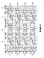
- the first embodiment of DRAM (dynamic RAM) is formed by a first memory cell array 1 and a second memory cell array 2, each comprising a matrix of a plurality of memory cells, a sensing amplifier array 3 comprising a plurality of sensing amplifiers 13 provided between two memory cell arrays 1 and 2, and an I/O line pair 4 on the other side of the first memory cell array 1 relative to the sensing amplifier array 3.
- Transistors 5 and 6 forming first switch means are provided between the first memory cell array 1 and the sensing amplifier array 3
- a transistor 7 forming second switch means is provided between the sensing amplifier array 3 and the second memory cell array 2.
- the memory cell arrays 1 and 2 are each formed by a matrix of memory cells, each of which is formed by an access transistor 11 and a capacitor 12.
- the gates of the access transistors 11 are connected to word lines WL1, WL2, Vietnamese, WL1′, WL2′, Vietnamese .
- One of the source and the drain of each access transistor 11 is connected to a bit line BL and BL , while the other of the source and the drain is connected to the capacitor 12.
- the bit lines BL and BL are paired. In Figure 1, the bit line pairs for the column numbers i to i+3 are shown for simplicity. These bit line pairs are selected by the turning on and off of column selection transistors 14 fed with column selection signals.
- the sensing amplifiers 13 making up the sensing amplifier array 3 are provided between the memory cell arrays 1 and 2, so that each sensing amplifier 13 is associated with one bit line pair BL and BL .
- the sensing amplifiers 13 are shared by the memory cell arrays 1 and 2, and operate to amplify the differential signal between the bit lines BL and BL extending across the memory cell arrays 1 and 2. That is, the sensing amplifiers 13 are so-called shared sensing amplifiers and, by the transistors 5, 6 and 7 of the first and second switching means as later described, divide the bit line pairs BL and BL extending across the memory cell arrays 1 and 2.
- the I/O line pair 4 is provided on the opposite side of the first memory cell array 1 from the sensing amplifier array 3.
- the I/O line pair 4, adjacent to the first memory cell array 1, is formed by an I/O line and an I/O line.
- the I/O line is connected via column selection transistors 14 to the bit line BL, while the I/O line is connected via column selection transistors 14 to the bit line BL . Data transfer is performed via the I/O line pair 4.
- the transistors 5 and 6 forming the first switch means electrically connect or disconnect the bit lines BL and BL between the first memory cell array 1 and the sensing amplifiers 13.
- the transistors 5 are connected in series with the paired bit lines selected by column selection signals Y i , Y i+2 , ... .
- To the gate of each of the transistors 5 is supplied a switching signal ⁇ ISO1, such that, when the switching signal 0 ⁇ ISO1 is at an H (high) level, the bit lines BL and BL and the associated sensing amplifier 13 are connected to each other and, when the switching signal 0 ⁇ ISO1 is at an L (low) level, the bit lines BL and BL and the sensing amplifier 13 are disconnected from each other.
- the transistors 6 forming the first switch means are connected in series with paired bit lines selected by column selection signals Y i+1 , Y i+3 , 7-8 .
- the bit columns controlled by the transistors 5 and the bit columns controlled by the transistors 6 are arrayed alternately, and the bit lines BL and BL are divided into a bit line group selected by the transistors 6 and a bit line group selected by the transistors 6.
- each transistor 6 To the gate of each transistor 6 is supplied a switching signal 0 ⁇ ISO2, such that, when the switching signal 0 ⁇ ISO2 is H, the bit lines BL and BL and the associated sensing amplifier 13 are connected to each other, and when the switching signal 0 ⁇ ISO2 is L, the bit lines BL and BL and the associated sensing amplifier 13 are disconnected from each other.
- the transistors 7 of the second switch means are provided in the bit lines BL and BL between the sensing amplifier array 3 and the memory cell array 2. To the gates of the transistors 7 is supplied a switching signal 0 ⁇ ISO0, such that, when the switching signal 0 ⁇ ISO0 is H, the transistors 7 are turned on and, when the switching signal 0 ⁇ ISO0 is L, the transistors 7 are turned off.
- transistors 15 and 16 forming a bit line loading circuit and an equalizer circuit are provided, and are controlled by a signal 0 ⁇ RES.
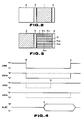
- the signal ⁇ RES goes at time t0 to L, while the signal 0 ⁇ ISO0 also goes to L, as indicated by solid lines in Figure 4.
- the transistors 15 and 16 are turned off, the transistors 7 of the second switch means also being turned off.
- the signals 0 ⁇ ISO1 and 0 ⁇ ISO2 are both H, so that the transistors 5 and 6 are turned on.
- the sensing amplifiers 13 are connected via the bit lines BL and BL only with the first memory cell array 1. After such activation of the first and second switch means, one of the word lines WL1′, WL2′, Vietnamese is selected by column address signals.
- the sensing operation of the sensing amplifier 13 the potentials of the bit lines BL and BL are amplified to H and L, respectively, in dependence on the data of the selected memory cell. Since the transistor 7 is turned off, and the transistors 5 and 6 are turned on, the parts of the bit lines BL and BL that are charged and discharged at this time are only those areas extending over the first memory cell array 1, as shown in Figure 2. The areas of the bit lines BL and BL extending over the second memory cell array 2 are not charged or discharged.
- the signal 0 ⁇ RES is changed from L to H, while the signal 0 ⁇ ISO0 is changed from L to H.
- the signal 0 ⁇ RES goes to L at time t0, as shown in Figure 4, while the signal 0 ⁇ ISO0 remains at H, as shown by a dashed line in Figure 4.
- the signals 0 ⁇ ISO1, and 0 ⁇ ISO2 controlling the transistors 5 and 6 are changed from H to L, as shown by dashed lines in Figure 4, so that the transistors 5 and 6 are turned off.
- the second memory cell array 2 is connected via the bit lines BL and BL to the sensing amplifiers 13.
- one of the word lines WL1, WL2, Vietnamese is selected by the column address signals.
- the sensing operation of the sensing amplifier 13 the potentials of the bit lines BL and BL are amplified to H and L, respectively, in dependence on the data of the selected memory cell. Since the transistor 7 is turned on and the transistors 5 and 6 are turned off, the parts of the bit lines BL and BL that are charged or discharged are limited to areas of the second memory cell array 2.
- the data of the selected memory cell are amplified by such activation of the sensing amplifiers 13. However, during reading or writing, it is necessary to turn the transistors 5 or 6 on selectively depending on the position of the accessed memory cell to connect the transistor 5 or 6 to the I/O lines.
- the signal 0 ⁇ ISO1 is changed at time t2 from L to H, as shown by a dashed line in Figure 4. Only the one bit line pair of the bit lines BL and BL extending into the first memory cell array 1, which is selected by the column selection signals Y i , Y i+2 , .
- bit lines are divided into two groups, so that when accessing the second memory cell 2, it is three-fourths of the overall area that is charged or discharged, whereas one-fourth of the overall area is not charged or discharged, so that the power consumption can be reduced.
- the signal 0 ⁇ RES is changed from L to H, while the signal 0 ⁇ ISO2 or 0 ⁇ ISO1 is changed from L to H.
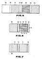
- a second embodiment of DRAM is so arranged that the number of the memory cell arrays, that is, the number of blocks, is double that of the DRAM of the preceding embodiment, with the control being made to provide for a constant power consumption.
- the DRAM shown therein is formed by two blocks, there being four memory cell arrays 51, 52, 53 and 54, there being a sensing amplifier array 55 between the memory cell arrays 51 and 52 and a sensing amplifier array 56 between the memory cell arrays 53 and 54.
- I/O line pairs 57 and 58 are provided between the memory cell arrays 51 and 53, so that the memory cell arrays 51 and 53 represent the first memory cell array having first switch means for dividing the bit lines into a plurality of groups.
- the number of memory cell arrays is twice that in the DRAM of the preceding embodiment, when one of the two blocks on respective sides of the I/O line pairs 57 and 58 is accessing the first memory cell array, the second memory cell array in the other block is accessed simultaneously.
- the areas shown by the hatched lines are those areas undergoing charging and discharging.
- the memory cell arrays 51 and 54 have memory cells being accessed, and the bit lines divided during the operation are only those associated with the memory cell array 53. As shown, it is five-eights of the overall area that undergoes charging or discharging, so that the power consumption is again reduced.
- the second memory cell array when the first memory cell array is accessed in one of the blocks, the second memory cell array is accessed in the other block.
- the block controlled by the solid line and the block controlled by the dashed line in Figure 4 are contiguous to each other. In this manner, the hatched line area in Figure 5 remains constant at all times, with the figure of five-eighth not being changed.
- the number of the blocks is not limited to two, and a similar control operation can be performed with respect to a larger number of blocks.
- bit lines are divided into three bit line groups.
- bit lines in a first memory cell array 61 are divided into a group of bit columns Ya, a group of bit columns Yb and a group of bit columns Yc.
- a sensing amplifier array 63 is provided between the first memory cell array 61 and a second memory cell array 62, and an I/O line pair 64 is provided on the other side of the first memory cell array 61 from the sensing amplifier array 63.
- first and second switch means are provided, with three signals being controlled by the first switch means.
- bit line group Ya, Yb and Yc undergoes charging or discharging during accessing of the second memory cell array 62. It is the bit line group associated with the bit lines Bl and BL associated in turn with the accessed memory cells that is selected.
- the power consumption can be reduced, while the speeding up of the operation is simultaneously achieved.
- the bit lines may be divided into four or more groups instead of three.
Landscapes
- Engineering & Computer Science (AREA)
- Microelectronics & Electronic Packaging (AREA)
- Computer Hardware Design (AREA)
- Dram (AREA)
Applications Claiming Priority (2)
| Application Number | Priority Date | Filing Date | Title |
|---|---|---|---|
| JP328895/87 | 1987-12-25 | ||
| JP62328895A JPH01171195A (ja) | 1987-12-25 | 1987-12-25 | メモリ装置 |
Publications (3)
| Publication Number | Publication Date |
|---|---|
| EP0323172A2 true EP0323172A2 (fr) | 1989-07-05 |
| EP0323172A3 EP0323172A3 (fr) | 1991-01-30 |
| EP0323172B1 EP0323172B1 (fr) | 1995-05-03 |
Family
ID=18215292
Family Applications (1)
| Application Number | Title | Priority Date | Filing Date |
|---|---|---|---|
| EP88312253A Expired - Lifetime EP0323172B1 (fr) | 1987-12-25 | 1988-12-22 | Mémoires dynamiques à accès aléatoire avec des amplificateurs de détection partagés |
Country Status (4)
| Country | Link |
|---|---|
| US (1) | US4916667A (fr) |
| EP (1) | EP0323172B1 (fr) |
| JP (1) | JPH01171195A (fr) |
| DE (1) | DE3853714D1 (fr) |
Cited By (3)
| Publication number | Priority date | Publication date | Assignee | Title |
|---|---|---|---|---|
| EP0640976A3 (fr) * | 1993-08-31 | 1995-10-11 | Oki Electric Ind Co Ltd | Dispositif de mémoire à semi-conducteurs et méthode d'opération. |
| GB2321734A (en) * | 1997-01-30 | 1998-08-05 | Motorola Inc | Circuit and method of latching a bit line in a non-volatile memory |
| EP0969473A1 (fr) * | 1998-06-29 | 2000-01-05 | Siemens Aktiengesellschaft | Amplificateur de détection entrelacé à circuit unilatéral de précharge |
Families Citing this family (24)
| Publication number | Priority date | Publication date | Assignee | Title |
|---|---|---|---|---|
| US5297097A (en) * | 1988-06-17 | 1994-03-22 | Hitachi Ltd. | Large scale integrated circuit for low voltage operation |
| USRE40132E1 (en) | 1988-06-17 | 2008-03-04 | Elpida Memory, Inc. | Large scale integrated circuit with sense amplifier circuits for low voltage operation |
| KR910009444B1 (ko) * | 1988-12-20 | 1991-11-16 | 삼성전자 주식회사 | 반도체 메모리 장치 |
| JPH02246516A (ja) * | 1989-03-20 | 1990-10-02 | Hitachi Ltd | 半導体装置 |
| US4964081A (en) * | 1989-08-11 | 1990-10-16 | Cray Research, Inc. | Read-while-write ram cell |
| US5426610A (en) * | 1990-03-01 | 1995-06-20 | Texas Instruments Incorporated | Storage circuitry using sense amplifier with temporary pause for voltage supply isolation |
| US5579273A (en) * | 1990-03-01 | 1996-11-26 | Texas Instruments Incorporated | Storage circuitry using sense amplifier shared between memories of differing number of rows |
| KR940008296B1 (ko) * | 1991-06-19 | 1994-09-10 | 삼성전자 주식회사 | 고속 센싱동작을 수행하는 센스앰프 |
| KR940007639B1 (ko) * | 1991-07-23 | 1994-08-22 | 삼성전자 주식회사 | 분할된 입출력 라인을 갖는 데이타 전송회로 |
| US5475642A (en) * | 1992-06-23 | 1995-12-12 | Taylor; David L. | Dynamic random access memory with bit line preamp/driver |
| US5339274A (en) * | 1992-10-30 | 1994-08-16 | International Business Machines Corporation | Variable bitline precharge voltage sensing technique for DRAM structures |
| US5715189A (en) * | 1993-04-13 | 1998-02-03 | Mitsubishi Denki Kabushiki Kaisha | Semiconductor memory device having hierarchical bit line arrangement |
| US5369622A (en) * | 1993-04-20 | 1994-11-29 | Micron Semiconductor, Inc. | Memory with isolated digit lines |
| US5754478A (en) | 1993-04-20 | 1998-05-19 | Micron Technology, Inc. | Fast, low power, write scheme for memory circuits using pulsed off isolation device |
| JPH06333386A (ja) * | 1993-05-20 | 1994-12-02 | Fujitsu Ltd | 半導体記憶装置 |
| KR0138881B1 (ko) * | 1993-07-07 | 1998-06-01 | 세끼모또 다다히로 | 반도체 메모리 장치 |
| JP3218844B2 (ja) * | 1994-03-22 | 2001-10-15 | 松下電器産業株式会社 | 半導体メモリ装置 |
| US5836007A (en) * | 1995-09-14 | 1998-11-10 | International Business Machines Corporation | Methods and systems for improving memory component size and access speed including splitting bit lines and alternate pre-charge/access cycles |
| US5835433A (en) * | 1997-06-09 | 1998-11-10 | Micron Technology, Inc. | Floating isolation gate from DRAM sensing |
| KR100464947B1 (ko) * | 1998-12-30 | 2005-05-20 | 주식회사 하이닉스반도체 | 디램의리프레시방법 |
| EP1181691B1 (fr) * | 2000-03-13 | 2005-08-24 | Infineon Technologies AG | Amplificateur d'ecriture/de lecture pour une cellule memoire dram, et memoire dram |
| US6479851B1 (en) * | 2000-05-16 | 2002-11-12 | Hynix Semiconductor, Inc. | Memory device with divided bit-line architecture |
| DE60032644T2 (de) * | 2000-06-29 | 2007-10-04 | Fujitsu Ltd., Kawasaki | Halbleiter-speicherbaustein |
| KR101997153B1 (ko) | 2013-04-01 | 2019-07-05 | 삼성전자주식회사 | 밸런싱 커패시터를 갖는 반도체 소자 및 그 형성 방법 |
Family Cites Families (8)
| Publication number | Priority date | Publication date | Assignee | Title |
|---|---|---|---|---|
| DE2919166C2 (de) * | 1978-05-12 | 1986-01-02 | Nippon Electric Co., Ltd., Tokio/Tokyo | Speichervorrichtung |
| JPS5873095A (ja) * | 1981-10-23 | 1983-05-02 | Toshiba Corp | ダイナミツク型メモリ装置 |
| JPS5880189A (ja) * | 1981-11-05 | 1983-05-14 | Fujitsu Ltd | 半導体記憶装置 |
| JPS592365A (ja) * | 1982-06-28 | 1984-01-07 | Fujitsu Ltd | ダイナミツク型半導体記憶装置 |
| US4656613A (en) * | 1984-08-29 | 1987-04-07 | Texas Instruments Incorporated | Semiconductor dynamic memory device with decoded active loads |
| JPS62114190A (ja) * | 1985-11-13 | 1987-05-25 | Mitsubishi Electric Corp | 半導体記憶装置 |
| JPS62197992A (ja) * | 1986-02-25 | 1987-09-01 | Mitsubishi Electric Corp | ダイナミツクram |
| JPH07111823B2 (ja) * | 1986-03-18 | 1995-11-29 | 三菱電機株式会社 | 半導体記憶装置 |
-
1987
- 1987-12-25 JP JP62328895A patent/JPH01171195A/ja active Pending
-
1988
- 1988-12-20 US US07/287,447 patent/US4916667A/en not_active Expired - Lifetime
- 1988-12-22 DE DE3853714T patent/DE3853714D1/de not_active Expired - Lifetime
- 1988-12-22 EP EP88312253A patent/EP0323172B1/fr not_active Expired - Lifetime
Cited By (5)
| Publication number | Priority date | Publication date | Assignee | Title |
|---|---|---|---|---|
| EP0640976A3 (fr) * | 1993-08-31 | 1995-10-11 | Oki Electric Ind Co Ltd | Dispositif de mémoire à semi-conducteurs et méthode d'opération. |
| US5511030A (en) * | 1993-08-31 | 1996-04-23 | Oki Electric Industry Co., Ltd. | Semiconductor memory device and method of driving same |
| GB2321734A (en) * | 1997-01-30 | 1998-08-05 | Motorola Inc | Circuit and method of latching a bit line in a non-volatile memory |
| EP0969473A1 (fr) * | 1998-06-29 | 2000-01-05 | Siemens Aktiengesellschaft | Amplificateur de détection entrelacé à circuit unilatéral de précharge |
| US6049492A (en) * | 1998-06-29 | 2000-04-11 | Siemens Aktiengesellschaft | Interleaved sense amplifier with a single-sided precharge device |
Also Published As
| Publication number | Publication date |
|---|---|
| US4916667A (en) | 1990-04-10 |
| DE3853714D1 (de) | 1995-06-08 |
| EP0323172B1 (fr) | 1995-05-03 |
| EP0323172A3 (fr) | 1991-01-30 |
| JPH01171195A (ja) | 1989-07-06 |
Similar Documents
| Publication | Publication Date | Title |
|---|---|---|
| EP0323172B1 (fr) | Mémoires dynamiques à accès aléatoire avec des amplificateurs de détection partagés | |
| US4367540A (en) | Dynamic memory with an interchangeable pair of data lines and sense amplifiers | |
| EP0359203B1 (fr) | Dispositif de mémoire à semi-conducteurs | |
| US7859930B2 (en) | Embedded memory databus architecture | |
| EP0037233B1 (fr) | Dispositif de mémoire à semi-conducteurs | |
| US4799197A (en) | Semiconductor memory device having a CMOS sense amplifier | |
| RU2170955C2 (ru) | Устройство полупроводниковой памяти для достижения высокой производительности и способ расположения в нем сигнальных шин | |
| EP0287120B1 (fr) | Dispositif de mémoire à semi-conducteurs avec un agencement d'amplificateurs de détection | |
| EP0264929B1 (fr) | Dispositif de mémoire à semi-conducteurs avec une disposition modifiée de lignes de bit | |
| US5677887A (en) | Semiconductor memory device having a large storage capacity and a high speed operation | |
| US4819209A (en) | Simultaneous dual access semiconductor memory device | |
| US6759280B2 (en) | Memory device with divided bit-line architecture | |
| EP0969473A1 (fr) | Amplificateur de détection entrelacé à circuit unilatéral de précharge | |
| EP0036932B1 (fr) | Système de détection de données et mémoire utilisant ce système | |
| US4980864A (en) | Semiconductor dynamic random access memory with relaxed pitch condition for sense amplifiers and method of operating the same | |
| JP3415420B2 (ja) | 半導体集積回路装置 | |
| US4559619A (en) | Large capacity memory circuit with improved write control circuit | |
| US6191996B1 (en) | Semiconductor memory device and data transmission method | |
| US20250118362A1 (en) | Banked sense amplifier circuit for a memory core and a memory core complex | |
| US5483495A (en) | Semiconductor memory device having dummy digit lines | |
| WO2002101748A2 (fr) | Amplificateur de detection et architecture pour reseaux numeriques ouverts | |
| JPH0743925B2 (ja) | 半導体記憶装置 | |
| US6333868B1 (en) | Semiconductor memory device having selectively shielded data lines | |
| GB2634266A (en) | Memory device, assist cell and double assist cell for a memory device | |
| JPS632197A (ja) | 半導体記憶装置 |
Legal Events
| Date | Code | Title | Description |
|---|---|---|---|
| PUAI | Public reference made under article 153(3) epc to a published international application that has entered the european phase |
Free format text: ORIGINAL CODE: 0009012 |
|
| AK | Designated contracting states |
Kind code of ref document: A2 Designated state(s): DE FR GB NL |
|
| PUAL | Search report despatched |
Free format text: ORIGINAL CODE: 0009013 |
|
| AK | Designated contracting states |
Kind code of ref document: A3 Designated state(s): DE FR GB NL |
|
| 17P | Request for examination filed |
Effective date: 19910605 |
|
| 17Q | First examination report despatched |
Effective date: 19930503 |
|
| GRAA | (expected) grant |
Free format text: ORIGINAL CODE: 0009210 |
|
| AK | Designated contracting states |
Kind code of ref document: B1 Designated state(s): DE FR GB NL |
|
| PG25 | Lapsed in a contracting state [announced via postgrant information from national office to epo] |
Ref country code: NL Free format text: LAPSE BECAUSE OF FAILURE TO SUBMIT A TRANSLATION OF THE DESCRIPTION OR TO PAY THE FEE WITHIN THE PRESCRIBED TIME-LIMIT Effective date: 19950503 Ref country code: FR Effective date: 19950503 |
|
| REF | Corresponds to: |
Ref document number: 3853714 Country of ref document: DE Date of ref document: 19950608 |
|
| PG25 | Lapsed in a contracting state [announced via postgrant information from national office to epo] |
Ref country code: DE Effective date: 19950804 |
|
| EN | Fr: translation not filed | ||
| NLV1 | Nl: lapsed or annulled due to failure to fulfill the requirements of art. 29p and 29m of the patents act | ||
| PG25 | Lapsed in a contracting state [announced via postgrant information from national office to epo] |
Ref country code: GB Effective date: 19951222 |
|
| PLBE | No opposition filed within time limit |
Free format text: ORIGINAL CODE: 0009261 |
|
| STAA | Information on the status of an ep patent application or granted ep patent |
Free format text: STATUS: NO OPPOSITION FILED WITHIN TIME LIMIT |
|
| 26N | No opposition filed | ||
| GBPC | Gb: european patent ceased through non-payment of renewal fee |
Effective date: 19951222 |