EP0413335A2 - Procédé pour connecter mutuellement des contacts d'électrodes - Google Patents
Procédé pour connecter mutuellement des contacts d'électrodes Download PDFInfo
- Publication number
- EP0413335A2 EP0413335A2 EP90115707A EP90115707A EP0413335A2 EP 0413335 A2 EP0413335 A2 EP 0413335A2 EP 90115707 A EP90115707 A EP 90115707A EP 90115707 A EP90115707 A EP 90115707A EP 0413335 A2 EP0413335 A2 EP 0413335A2
- Authority
- EP
- European Patent Office
- Prior art keywords
- circuit substrate
- semiconductor device
- electroconductive
- electroconductive particles
- electrode terminals
- Prior art date
- Legal status (The legal status is an assumption and is not a legal conclusion. Google has not performed a legal analysis and makes no representation as to the accuracy of the status listed.)
- Granted
Links
Images





Classifications
-
- G—PHYSICS
- G02—OPTICS
- G02F—OPTICAL DEVICES OR ARRANGEMENTS FOR THE CONTROL OF LIGHT BY MODIFICATION OF THE OPTICAL PROPERTIES OF THE MEDIA OF THE ELEMENTS INVOLVED THEREIN; NON-LINEAR OPTICS; FREQUENCY-CHANGING OF LIGHT; OPTICAL LOGIC ELEMENTS; OPTICAL ANALOGUE/DIGITAL CONVERTERS
- G02F1/00—Devices or arrangements for the control of the intensity, colour, phase, polarisation or direction of light arriving from an independent light source, e.g. switching, gating or modulating; Non-linear optics
- G02F1/01—Devices or arrangements for the control of the intensity, colour, phase, polarisation or direction of light arriving from an independent light source, e.g. switching, gating or modulating; Non-linear optics for the control of the intensity, phase, polarisation or colour
- G02F1/13—Devices or arrangements for the control of the intensity, colour, phase, polarisation or direction of light arriving from an independent light source, e.g. switching, gating or modulating; Non-linear optics for the control of the intensity, phase, polarisation or colour based on liquid crystals, e.g. single liquid crystal display cells
- G02F1/133—Constructional arrangements; Operation of liquid crystal cells; Circuit arrangements
- G02F1/1333—Constructional arrangements; Manufacturing methods
- G02F1/1345—Conductors connecting electrodes to cell terminals
- G02F1/13452—Conductors connecting driver circuitry and terminals of panels
-
- H—ELECTRICITY
- H05—ELECTRIC TECHNIQUES NOT OTHERWISE PROVIDED FOR
- H05K—PRINTED CIRCUITS; CASINGS OR CONSTRUCTIONAL DETAILS OF ELECTRIC APPARATUS; MANUFACTURE OF ASSEMBLAGES OF ELECTRICAL COMPONENTS
- H05K3/00—Apparatus or processes for manufacturing printed circuits
- H05K3/30—Assembling printed circuits with electric components, e.g. with resistors
- H05K3/32—Assembling printed circuits with electric components, e.g. with resistors electrically connecting electric components or wires to printed circuits
- H05K3/321—Assembling printed circuits with electric components, e.g. with resistors electrically connecting electric components or wires to printed circuits by conductive adhesives
-
- H—ELECTRICITY
- H10—SEMICONDUCTOR DEVICES; ELECTRIC SOLID-STATE DEVICES NOT OTHERWISE PROVIDED FOR
- H10W—GENERIC PACKAGES, INTERCONNECTIONS, CONNECTORS OR OTHER CONSTRUCTIONAL DETAILS OF DEVICES COVERED BY CLASS H10
- H10W70/00—Package substrates; Interposers; Redistribution layers [RDL]
- H10W70/60—Insulating or insulated package substrates; Interposers; Redistribution layers
- H10W70/62—Insulating or insulated package substrates; Interposers; Redistribution layers characterised by their interconnections
- H10W70/66—Conductive materials thereof
- H10W70/666—Organic materials or pastes
-
- H—ELECTRICITY
- H10—SEMICONDUCTOR DEVICES; ELECTRIC SOLID-STATE DEVICES NOT OTHERWISE PROVIDED FOR
- H10W—GENERIC PACKAGES, INTERCONNECTIONS, CONNECTORS OR OTHER CONSTRUCTIONAL DETAILS OF DEVICES COVERED BY CLASS H10
- H10W72/00—Interconnections or connectors in packages
- H10W72/01—Manufacture or treatment
- H10W72/011—Apparatus therefor
-
- H—ELECTRICITY
- H10—SEMICONDUCTOR DEVICES; ELECTRIC SOLID-STATE DEVICES NOT OTHERWISE PROVIDED FOR
- H10W—GENERIC PACKAGES, INTERCONNECTIONS, CONNECTORS OR OTHER CONSTRUCTIONAL DETAILS OF DEVICES COVERED BY CLASS H10
- H10W74/00—Encapsulations, e.g. protective coatings
- H10W74/01—Manufacture or treatment
- H10W74/012—Manufacture or treatment of encapsulations on active surfaces of flip-chip devices, e.g. forming underfills
-
- H—ELECTRICITY
- H10—SEMICONDUCTOR DEVICES; ELECTRIC SOLID-STATE DEVICES NOT OTHERWISE PROVIDED FOR
- H10W—GENERIC PACKAGES, INTERCONNECTIONS, CONNECTORS OR OTHER CONSTRUCTIONAL DETAILS OF DEVICES COVERED BY CLASS H10
- H10W74/00—Encapsulations, e.g. protective coatings
- H10W74/10—Encapsulations, e.g. protective coatings characterised by their shape or disposition
- H10W74/15—Encapsulations, e.g. protective coatings characterised by their shape or disposition on active surfaces of flip-chip devices, e.g. underfills
-
- H—ELECTRICITY
- H05—ELECTRIC TECHNIQUES NOT OTHERWISE PROVIDED FOR
- H05K—PRINTED CIRCUITS; CASINGS OR CONSTRUCTIONAL DETAILS OF ELECTRIC APPARATUS; MANUFACTURE OF ASSEMBLAGES OF ELECTRICAL COMPONENTS
- H05K2201/00—Indexing scheme relating to printed circuits covered by H05K1/00
- H05K2201/10—Details of components or other objects attached to or integrated in a printed circuit board
- H05K2201/10613—Details of electrical connections of non-printed components, e.g. special leads
- H05K2201/10621—Components characterised by their electrical contacts
- H05K2201/10674—Flip chip
-
- H—ELECTRICITY
- H05—ELECTRIC TECHNIQUES NOT OTHERWISE PROVIDED FOR
- H05K—PRINTED CIRCUITS; CASINGS OR CONSTRUCTIONAL DETAILS OF ELECTRIC APPARATUS; MANUFACTURE OF ASSEMBLAGES OF ELECTRICAL COMPONENTS
- H05K2201/00—Indexing scheme relating to printed circuits covered by H05K1/00
- H05K2201/10—Details of components or other objects attached to or integrated in a printed circuit board
- H05K2201/10613—Details of electrical connections of non-printed components, e.g. special leads
- H05K2201/10954—Other details of electrical connections
- H05K2201/10977—Encapsulated connections
-
- H—ELECTRICITY
- H05—ELECTRIC TECHNIQUES NOT OTHERWISE PROVIDED FOR
- H05K—PRINTED CIRCUITS; CASINGS OR CONSTRUCTIONAL DETAILS OF ELECTRIC APPARATUS; MANUFACTURE OF ASSEMBLAGES OF ELECTRICAL COMPONENTS
- H05K2203/00—Indexing scheme relating to apparatus or processes for manufacturing printed circuits covered by H05K3/00
- H05K2203/10—Using electric, magnetic and electromagnetic fields; Using laser light
- H05K2203/105—Using an electrical field; Special methods of applying an electric potential
-
- H—ELECTRICITY
- H05—ELECTRIC TECHNIQUES NOT OTHERWISE PROVIDED FOR
- H05K—PRINTED CIRCUITS; CASINGS OR CONSTRUCTIONAL DETAILS OF ELECTRIC APPARATUS; MANUFACTURE OF ASSEMBLAGES OF ELECTRICAL COMPONENTS
- H05K3/00—Apparatus or processes for manufacturing printed circuits
- H05K3/10—Apparatus or processes for manufacturing printed circuits in which conductive material is applied to the insulating support in such a manner as to form the desired conductive pattern
- H05K3/102—Apparatus or processes for manufacturing printed circuits in which conductive material is applied to the insulating support in such a manner as to form the desired conductive pattern by bonding of conductive powder, i.e. metallic powder
-
- H—ELECTRICITY
- H05—ELECTRIC TECHNIQUES NOT OTHERWISE PROVIDED FOR
- H05K—PRINTED CIRCUITS; CASINGS OR CONSTRUCTIONAL DETAILS OF ELECTRIC APPARATUS; MANUFACTURE OF ASSEMBLAGES OF ELECTRICAL COMPONENTS
- H05K3/00—Apparatus or processes for manufacturing printed circuits
- H05K3/22—Secondary treatment of printed circuits
- H05K3/28—Applying non-metallic protective coatings
- H05K3/281—Applying non-metallic protective coatings by means of a preformed insulating foil
-
- H—ELECTRICITY
- H10—SEMICONDUCTOR DEVICES; ELECTRIC SOLID-STATE DEVICES NOT OTHERWISE PROVIDED FOR
- H10W—GENERIC PACKAGES, INTERCONNECTIONS, CONNECTORS OR OTHER CONSTRUCTIONAL DETAILS OF DEVICES COVERED BY CLASS H10
- H10W72/00—Interconnections or connectors in packages
- H10W72/071—Connecting or disconnecting
- H10W72/072—Connecting or disconnecting of bump connectors
- H10W72/07231—Techniques
- H10W72/07236—Soldering or alloying
-
- H—ELECTRICITY
- H10—SEMICONDUCTOR DEVICES; ELECTRIC SOLID-STATE DEVICES NOT OTHERWISE PROVIDED FOR
- H10W—GENERIC PACKAGES, INTERCONNECTIONS, CONNECTORS OR OTHER CONSTRUCTIONAL DETAILS OF DEVICES COVERED BY CLASS H10
- H10W72/00—Interconnections or connectors in packages
- H10W72/071—Connecting or disconnecting
- H10W72/072—Connecting or disconnecting of bump connectors
- H10W72/07251—Connecting or disconnecting of bump connectors characterised by changes in properties of the bump connectors during connecting
- H10W72/07254—Connecting or disconnecting of bump connectors characterised by changes in properties of the bump connectors during connecting changes in dispositions
-
- H—ELECTRICITY
- H10—SEMICONDUCTOR DEVICES; ELECTRIC SOLID-STATE DEVICES NOT OTHERWISE PROVIDED FOR
- H10W—GENERIC PACKAGES, INTERCONNECTIONS, CONNECTORS OR OTHER CONSTRUCTIONAL DETAILS OF DEVICES COVERED BY CLASS H10
- H10W72/00—Interconnections or connectors in packages
- H10W72/071—Connecting or disconnecting
- H10W72/073—Connecting or disconnecting of die-attach connectors
-
- H—ELECTRICITY
- H10—SEMICONDUCTOR DEVICES; ELECTRIC SOLID-STATE DEVICES NOT OTHERWISE PROVIDED FOR
- H10W—GENERIC PACKAGES, INTERCONNECTIONS, CONNECTORS OR OTHER CONSTRUCTIONAL DETAILS OF DEVICES COVERED BY CLASS H10
- H10W72/00—Interconnections or connectors in packages
- H10W72/071—Connecting or disconnecting
- H10W72/073—Connecting or disconnecting of die-attach connectors
- H10W72/07331—Connecting techniques
-
- H—ELECTRICITY
- H10—SEMICONDUCTOR DEVICES; ELECTRIC SOLID-STATE DEVICES NOT OTHERWISE PROVIDED FOR
- H10W—GENERIC PACKAGES, INTERCONNECTIONS, CONNECTORS OR OTHER CONSTRUCTIONAL DETAILS OF DEVICES COVERED BY CLASS H10
- H10W72/00—Interconnections or connectors in packages
- H10W72/20—Bump connectors, e.g. solder bumps or copper pillars; Dummy bumps; Thermal bumps
- H10W72/221—Structures or relative sizes
- H10W72/224—Bumps having multiple side-by-side cores
-
- H—ELECTRICITY
- H10—SEMICONDUCTOR DEVICES; ELECTRIC SOLID-STATE DEVICES NOT OTHERWISE PROVIDED FOR
- H10W—GENERIC PACKAGES, INTERCONNECTIONS, CONNECTORS OR OTHER CONSTRUCTIONAL DETAILS OF DEVICES COVERED BY CLASS H10
- H10W72/00—Interconnections or connectors in packages
- H10W72/20—Bump connectors, e.g. solder bumps or copper pillars; Dummy bumps; Thermal bumps
- H10W72/241—Dispositions, e.g. layouts
- H10W72/244—Dispositions, e.g. layouts relative to underlying supporting features, e.g. bond pads, RDLs or vias
-
- H—ELECTRICITY
- H10—SEMICONDUCTOR DEVICES; ELECTRIC SOLID-STATE DEVICES NOT OTHERWISE PROVIDED FOR
- H10W—GENERIC PACKAGES, INTERCONNECTIONS, CONNECTORS OR OTHER CONSTRUCTIONAL DETAILS OF DEVICES COVERED BY CLASS H10
- H10W72/00—Interconnections or connectors in packages
- H10W72/20—Bump connectors, e.g. solder bumps or copper pillars; Dummy bumps; Thermal bumps
- H10W72/241—Dispositions, e.g. layouts
- H10W72/247—Dispositions of multiple bumps
-
- H—ELECTRICITY
- H10—SEMICONDUCTOR DEVICES; ELECTRIC SOLID-STATE DEVICES NOT OTHERWISE PROVIDED FOR
- H10W—GENERIC PACKAGES, INTERCONNECTIONS, CONNECTORS OR OTHER CONSTRUCTIONAL DETAILS OF DEVICES COVERED BY CLASS H10
- H10W90/00—Package configurations
- H10W90/701—Package configurations characterised by the relative positions of pads or connectors relative to package parts
- H10W90/721—Package configurations characterised by the relative positions of pads or connectors relative to package parts of bump connectors
- H10W90/724—Package configurations characterised by the relative positions of pads or connectors relative to package parts of bump connectors between a chip and a stacked insulating package substrate, interposer or RDL
-
- H—ELECTRICITY
- H10—SEMICONDUCTOR DEVICES; ELECTRIC SOLID-STATE DEVICES NOT OTHERWISE PROVIDED FOR
- H10W—GENERIC PACKAGES, INTERCONNECTIONS, CONNECTORS OR OTHER CONSTRUCTIONAL DETAILS OF DEVICES COVERED BY CLASS H10
- H10W90/00—Package configurations
- H10W90/701—Package configurations characterised by the relative positions of pads or connectors relative to package parts
- H10W90/731—Package configurations characterised by the relative positions of pads or connectors relative to package parts of die-attach connectors
- H10W90/734—Package configurations characterised by the relative positions of pads or connectors relative to package parts of die-attach connectors between a chip and a stacked insulating package substrate, interposer or RDL
Definitions
- the present invention relates to a method of mutually connecting electrically electrode terminals of circuit plates or substrates disposed opposite to each other by electroconductive (fine) particles.
- the present invention further relates to a method of connecting a semiconductor device or chip to a circuit plate or substrate by the face-down bonding mode.
- an anisotropically conductive adhesive film has been used for mutually connecting lead or takeout electrodes disposed on circuit substrates at a density of about 5 lines/mm.
- connection using an anisotropically conductive adhesive film involves a problem that insulation between adjacent electrodes is not ensured if the connection terminal density is increased to 10 electrodes or more per mm.
- a principal object of the present invention is to provide a method of mutually connecting electrode terminals by which a reliable connection is provided even when applied to electrode terminals disposed at a high density and which can be performed economically to provide a high production yield.
- Another object of the present invention is to provide a method of connecting a semiconductor device by which a semiconductor device is connected to a circuit substrate without forming bump contacts on the semiconductor device, thus providing an increased production yield of the semiconductor device, a decrease in production cost and an increased reliability, even when the connection is effected by the face-down bonding mode.
- a method of mutually connecting electrode terminals formed on a pair of circuit substrates to be connected comprising: dispersing charged electroconductive particles onto at least one of the circuit substrates to selectively attach the electroconductive particles onto the electrode terminals thereof, and sandwiching the electroconductive particles between the electrode terminals of the pair of circuit substrates to mutually connect the electrode terminals electrically.
- the term circuit substrate is intended to cover an electrical element, such as a semiconductor device or IC chip having electrode terminals for connection formed thereon.
- a method of mutual connection of electrode terminals for electrically connecting and mutually fixing an electrode terminal formed on a first electrical circuit substrate and an electrode terminal formed on a second circuit substrate comprising: dispersing electroconductive particles onto at least one of the first and second circuit substrates to selectively attach the electroconductive particles onto the electrode terminal formed thereon, and then bonding the electrode terminal formed on the first circuit substrate with the electrode terminal formed on the second circuit substrate.
- a method of a method of mutual connection of electrode terminals for electrically connecting and mutually fixing an electrode terminal formed on a first electrical circuit substrate and an electrode terminal formed on a second circuit substrate comprising: charging electroconductive particles by passing the electroconductive particles through a charging zone in which a charging electric field is formed; dispersing electroconductive particles onto at least one of the first and second circuit substrates to selectively attach the electroconductive particles onto the electrode terminal formed thereon, and then bonding the electrode terminal formed on the first circuit substrate with the electrode terminal formed on the second circuit substrate.
- a method of a method of connecting a semiconductor device to a circuit substrate after positional alignment between electrode pads of the semiconductor device and electrode terminals of the circuit substrate comprising: applying a paste comprising a mixture of an electroconductive resin and electroconductive particles onto at least one of the electrode pads of the semiconductor device and the electrode terminals of the circuit substrate, and hardening the electroconductive resin while pressing the electrode pads of the semiconductor device against the electrode terminals of the circuit substrate.
- the electroconductive particles when electroconductive particles are dispersed and attached to electrode terminals of circuit substrates to be mutually connected, the electroconductive particles are selectively attached to the electrode terminals, so that the electrode terminals disposed at a high density on the circuit substrates are mutually connected while ensuring insulation between adjacent electrode terminals.
- the electroconductive particles are charged and dispersed in an electrostatic field concentrated at the electrode terminals so as to control the position where the electroconductive particles are attached, thus attaching a larger amount of the electroconductive particles to the electrode terminals.
- the electroconductive particles may be charged by corona discharging or triboelectrification through friction with an insulating or semiconductor material. Further, by coating the electrode terminals except for the connecting parts thereof with an insulating film, the electric field may be concentrated at the connecting parts of the electrode terminals so that the electroconductive particles can be selectively attached to the connecting parts.
- the electrode terminals are allowed to have a lower specific gravity so that they can be easily guided to the electrode terminals, and a stress acting at the connected parts can be alleviated after the mutual connection of the circuit substrates.
- connection may be effected without using bump contacts on the semiconductor device by dispersing and selectively attaching electroconductive particles to the electrode terminals on the circuit substrate, aligning the electrode pads of the semiconductor device and bonding them with an adhesive.
- a part of the circuit substrate facing the die edge of the semiconductor device may be covered with an insulating film, whereby the electroconductive particles may be dispersed so that they are not attached to the part facing the die edge.
- charged electroconductive particles are dispersed on at least one of one circuit substrate and the other circuit substrate or electrical element to be connected to each other so as to selectively attach the electroconductive particle to the electrode terminals thereof, and the electroconductive particles are sandwiched between the electrode terminals of both substrates so as to mutually connect the electrode terminals, wherein an insulating mask is disposed to cover a part to which the electroconductive particles need not be attached at the time of selective dispersion of the electroconductive particles.
- the insulating mask may for example be applied onto a circuit substrate by means of an adhesive.
- the thickness, dielectric constant and shape of the insulating mask may be appropriately selected in view of factors, such as the charge, quantity, dispersion pressure, dispersion height and selectivity of dispersion and attachment of the electroconductive particles.
- an electric field directed to electrode terminals may be generated so that electroconductive particles are guided to the electrode terminals and, as part to which electroconductive particles are not dispersed (non-selection region) is covered by an insulating mask, the electroconductive particles are prevented from being attached to patterned electrodes extending from the electrode terminals of the circuit substrate and electroconductive particles are attached to only the desired portion of the electrode terminals.
- the electroconductive particles are dispersed for selective attachment after an insulating mask is intimately disposed, a thick insulating film of a high dielectric constant need not be formed on a circuit substrate but a thin insulating film, if used, is sufficient or such an insulating film can be omitted depending on the usage, so that the connection is performed at a low cost.
- the electroconductive particles are attached to only desired parts on the electrode terminals at a high selectivity, so that the connection may be performed without the occurrence of a short circuit between the die edge part of an IC chip and the electrode pattern on the circuit substrate or an electrical failure due to the formation of a capacitive load in combination with an insulating film.
- Figure 1 is a schematic view illustrating a system of dispersing electroconductive particles according to an embodiment of the present invention.
- the system includes a line 1 for introducing a liquid dispersion of electroconductive particles, a line 2 for introducing liquid nitrogen, a discharge nozzle 3, an electrical discharge electrode 5, a high-voltage power supply 6 connected to the discharge electrode 5 for forming a corona electric field, a circuit substrate 11, an electrode terminal 8 on the circuit substrate 11, a mask 10 covering a prescribed part of the circuit substrate 11 and a grounding line 12 connected to the electrode terminal 8.
- the liquid dispersion of electroconductive particles supplied through the line 1 is sprayed for dispersion through the discharge nozzle 4 under the action of the compressed nitrogen supplied through the line 2 to form electroconductive particles 4, which are then passed to be charged through a corona electric field formed by the discharge electrode.
- the thus-formed charged electroconductive particles 7 are guided along electric lines of force in an electrostatic field formed between the discharge electrode 5 and the grounded lead electrodes 8 on the circuit substrate 11, to be attached to the connecting part of the lead electrodes 8.
- FIG 2 is a sectional view taken along the line X-X′ in Figure 1, wherein the electrode terminals attached to the lead electrodes 8 are denoted by a reference numeral 9.
- the electroconductive particles can be selectively dispersed and attached concentratively to the part used for connection of the electrode terminals 8, so that the connection is performed with a high degree of insulation between adjacent electrodes.
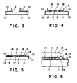
- connecting parts a and b are formed on pattern electrodes (electrode terminals) 13 on a glass substrate 11, the pattern electrodes 13 except for the connecting parts a and b are covered with an intimately disposed insulating mask (insulating film) 10, and electroconductive particles 9 are dispersed in a manner as shown in Figure 1 to be selectively attached to the connecting parts a and b .
- electrode pads 16 of a semiconductor device 15 are aligned with the glass substrate 11, and an adhesive 17 applied at parts other than the connecting parts is hardened or cured while applying a pressure between the semiconductor device 15 and the substrate 11, thereby to electrically connect the electrode terminals of the liquid crystal device and the electrode pads of the semiconductor device.
- the adhesive 17 is one which can be released by application of heat, cooling, ultrasonic wave or solvent, the semiconductor device connected as described can be removed and easily replaced by a new one if the inadequacy of the connected device is found by the operation test at this stage.
- Figure 5 shows a state wherein the non-bonded parts between the semiconductor device and the glass substrate after the operation test of the semiconductor device are bonded and sealed up by an adhesive 18 comprising mainly a thermosetting resin.
- Figure 6 schematically shows a state wherein edge short circuit between the die edge of a semiconductor device and a lead electrode of a liquid crystal substrate is caused by an electroconductive particle in case where the lead electrode on the liquid crystal substrate facing the die edge of the semiconductor device is not covered by such an insulating film.
- Figure 19 shows a passivation film formed on the semiconductor device and shows a state where an electroconductive particle 9a causes a short circuit between the die edge 14 and the lead electrode 13.
- metal particles as the electroconductive particles for selective scattering and electrical connection, but those formed by coating resin particles with an electroconductive plating can be more easily guided along electric lines of force because of a smaller specific gravity than metal particles. Further, as for the electrical connection by the contact with the electroconductive particles, the resin particles can relax a stress acting at the contacts to provide an improved reliability.
- Figure 7 shows another embodiment of the present invention, wherein electroconductive particles 9 are attached to electrode terminals 13 on a glass substrate 11 of a liquid crystal device, electrode terminals 22 on a flexible circuit substrate 21 are aligned with the electrode terminals 13 on the glass substrate 11, and an adhesive 23 is cured under pressure to effect the connection.
- the adhesive 23 may comprise a thermoplastic resin, a thermosetting resin or mixture of a thermosetting resin and a thermoplastic resin.
- the adhesive 23 may be supplied by applying a liquid adhesive at the periphery of the flexible circuit substrate 21 so as to cause the penetration thereof from the periphery, by applying, screenprinting or transferring an adhesive onto one or both of the flexible circuit substrate 21 and the liquid crystal substrate 11, by interposing an adhesive in the form of a sheet between the flexible substrate 21 and the liquid crystal substrate 11, or by applying an adhesive in the form of a sheet onto one or both of the flexible circuit substrate 21 and the liquid crystal substrate 11.
- FIG 8 is a plan view showing a state wherein electroconductive particles were dispersed and attached in a specific embodiment of the present invention.
- electroconductive particles 9 were attached to the connecting parts a of the patterned electrodes and not to the insulating parts (the circuit substrate 11 and the insulating mask 10).
- the selectivity of dispersion between the electrode patterns ratio of the number of electroconductive particles dispersed and attached to the connecting parts/the number of electroconductive particles dispersed and attached to the insulating parts of the circuit substrate
- electroconductive particles may preferably have a volume-average particle size of 0.1- 50 microns, particularly 1 - 20 microns, and the electroconductive coating thickness thereof may preferably be 1x10 ⁇ 4 to 5x10 ⁇ 2 times, particularly 1x10 ⁇ 3 to 1x10 ⁇ 2 times, the average particle size of the electroconductive particles.
- Electroconductive particles may preferably be substantially spherical.
- Another commercial available embodiment may include "MICROPEARL Au" (mfd. by Sekisui Fine Chemical K.K.).
- Figure 9 shows a modification of the embodiment shown in Figure 3.
- an insulating mask 10 is applied to a circuit substrate 11 by the medium of an adhesive, whereby the insulating mask need not be repetitively removed.
- a semiconductor device for driving a liquid crystal device is connected to lead electrodes formed on a glass substrate of the liquid crystal device by the face-down bonding mode.
- FIG 10 is a schematic view of an apparatus according to the present invention.
- electroconductive particles comprising plastic beads (having an average particle size of 0.1- 100 microns) coated with a film of, e.g., gold, silver, aluminum, nickel, chromium or an alloy of these metals are charged to form charged particles 10b while they are passed through a single-polarity bi-directional particle charger 12 called a boxer charger (e.g., one available from Masuda Kenkyusho, Co. Ltd., Japan).
- the system further includes a glass substrate for a liquid crystal display device, lead electrodes 14 formed on the substrate, an insulating film 15 having an opening A exposing the connecting parts of the lead electrodes 14, grounding lines 16 for the lead electrodes 14 and an external power supply 17.
- the lead electrodes 14 formed on the glass substrate 13 are grounded, the lead electrodes 14 are covered with the insulating film 15 except for the connecting parts thereof, and then the electroconductive particles 10a charged by means of the boxer charger (particle charger) to be dispersed onto the lead electrodes 14.
- the boxer charger particle charger
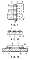
- Figure 11 is a partial plan view of a part X in Figure 10 from the above.
- the electroconductive particles 10b in the vicinity of the opening A of the insulating film cause an image force acing in the neighborhood of the lead electrodes 14 and therefore are preferentially attached to the lead electrodes 14.
- Figure 12 shows a state wherein charged electroconductive particles 10c (corresponding to electroconductive particles 10b shown in Figure 10) are attached to the lead electrodes 14.
- the insulating film 15 is removed and electrode pads 19 of a semiconductor device 18 are aligned with its face directed downward with the lead electrodes 14, and an insulating adhesive 20 is cured under pressure to effect the connection.
- Figure 14 is a schematic sectional view of the boxer charger used in the present invention, and figure 15 is a plan view thereof.
- the system includes a ceramic cylinder 501, discharge electrodes 502, exciting electrodes 503, electroconductive particles 504A, charged electroconductive particles 504B, a charging zone (charging space) 505, a charging electric field E, exciting transformers TR1 and TR2, a main transformer TR3, amplifiers 506, 507 and 508, gates 509 and 510, a phase shifter 511, a main power supply 512 of 500 Hz, and an exciting power supply 513 of 20 kHz.
- the charging electric field E is formed by applying an AC voltage of 500 Hz from tha main power supply 512 to the discharge electrodes 502. If a high-frequency AC voltage of 20 kHz is applied to the exciting electrodes 503 when the discharge electrodes 502 on the S1 side are negative, a planar plasma ion source is formed due to surface discharge, and only negative ions are pulled out due to the electric field, fly through the charging space and are absorbed at the non-excited surface on the side S2. During this period, the negative ions collided against the particles 504A from the left thereof to charge the particles.
- the distance between S1 and S2 may be set within the range of 1 - 10 cm, preferably 2 - 5 cm, and the height of the ceramic cylinder may be set within the range of 3 - 20 cm, preferably 5 - 10 cm.
- Figures 16A - 16C show a voltage waveform applied between the discharge electrodes on the sides S1 and S2, a voltage waveform applied to the exciting electrode 503 on the S1 side, and a voltage waveform applied to the exciting electrode 504, respectively, shown on a common time scale.
- a semiconductor device may be connected to a circuit substrate in the face-down bonding mode by applying a paste mixture comprising electroconductive particles (preferably spherical ones) and an electroconductive resin onto at least one of the electrode pads of the semiconductor device and the electrode terminals of the circuit substrate, positionally aligning the electrode pads of the semiconductor device and the electrode terminals of the circuit substrate, and applying at least one energy such as those of heat, ultraviolet rays and radiations to cure the electroconductive resin while pressing the semiconductor device onto the circuit substrate, to electrically connect the electrode pads of the semiconductor device with the electrode terminals of the circuit substrate.
- a paste mixture comprising electroconductive particles (preferably spherical ones) and an electroconductive resin onto at least one of the electrode pads of the semiconductor device and the electrode terminals of the circuit substrate, positionally aligning the electrode pads of the semiconductor device and the electrode terminals of the circuit substrate, and applying at least one energy such as those of heat, ultraviolet rays and radiations to cure the electroconductive resin while pressing the semiconductor device onto the circuit substrate, to electrically connect the electrode pads
- the electroconductive particles are sandwiched between the electrode pads of the semiconductor device and the electrode terminals of the circuit substrate, whereby the spacing between the electrode pads of the semiconductor device and the electrode terminals of the circuit substrate may be specifically set and the electrode pads of the semiconductor device and the electrode terminals of the circuit substrate are electrically connected to each other.
- the electroconductive resin functions to hold the spacing between the electrode pads of the semiconductor device and the electrode terminals of the circuit substrate and also supplements the electrical connection therebetween.
- the electroconductive particles comprise preferably spherical resin particles coated with an electroconductive plating, the contact area between the electrode pads of the semiconductor device and the electrode terminals of the circuit substrate can be increased and further the stress at the connecting parts can be alleviated.
- Figure 17 illustrates such an embodiment according to the connection method of the present invention, particularly a state of a connecting part in a case where a semiconductor device is connected to lead electrodes of a circuit substrate by the face-down bonding mode.
- a paste comprising a mixture of electroconductive particles 171 and an electroconductive resin 172 is disposed between electrode pads 173 of a semiconductor device 178 and lead electrodes 174 of a circuit substrate 177 (by application to either one or both sides), the circuit substrate 178 is pressed so that spacing between the electrode pads 173 and the electrode terminals 174 becomes even smaller than the average particle size of the electroconductive particles 171, and the electroconductive resin 172 is hardened while the electroconductive particles 171 are sandwiched between the electrode pads 173 and the electrode terminals 174, followed by releasing the pressure.
- the electroconductive resin may be hardened by heating if it is of a thermosetting type. If the electroconductive resin 172 contains a thermoplastic resin, the semiconductor device can be removed relatively easily when some disorder is found after the hardening of the electroconductive resin 172.
- the base substrate 177 of the circuit substrate is transparent, it is possible to use a ultraviolet-curable electroconductive resin for the electroconductive resin 172.
- the semiconductor device is pressed so as to sandwich the electroconductive particles 171 between the electrode pads 173 and the electrode terminals 174, and in this state, the electroconductive resin 172 is cured by irradiation with ultraviolet rays emitted through the base substrate 177 from the lower side.
- resin particles coated with a metal plating are used as the electroconductive resins 171 but spherical metal particles may also be used.
- the spacing between the electrode pads 173 and the electrode terminals 174 can be made constant and the connection resistance by the contact with electroconductive particles can be made stable.
- Figures 18A - 18D show an embodiment of connecting a semiconductor device for driving a liquid crystal device to lead electrodes on a glass substrate of the liquid crystal device in the face-down bonding mode.
- a paste comprising a mixture of electroconductive particles 171 obtained by coating spherical resin particles with a Ni plating and an electroconductive resin 172 of an ultraviolet-curable-type containing Ag powder as an electroconductive element is applied on lead electrodes 174 formed on a glass substrate 177 of a liquid crystal device, and electrode pads 173 of a semiconductor device are aligned with the electrode terminals 174.
- the semiconductor device 178 is pressed by a pressing member 179 so as to sandwich and hold tha electroconductive particles 171 between the electrode pads 173 and the electrode terminals 174 on the glass substrate 177.
- the electroconductive resin 172 is hardened by irradiation with ultraviolet rays entering from below the glass substrate to electrically connect the electrode pads 173 of the semiconductor device and the electrode terminals 174 on the glass substrate.
- the pressure from the pressing member 172 may be released while retaining the electrical connection.
- an operation test of the semiconductor device may be performed, and if some operation failure is found, the semiconductor device can be removed by some means such as heating, cooling, application ultrasonic wave or solvent, followed by connection of a new semiconductor device.
- an adhesive 180 comprising principally a thermosetting resin is applied for bonding and sealing of the non-bonded parts between the semiconductor device and the glass substrate.
- thermosetting electroconductive resin it is also possible to use a thermosetting electroconductive resin as the electroconductive resin 172.
- Electroconductive (fine) particles may be attached to a circuit substrate through dispersion, so that the attachment of the electroconductive particles can be effected without restriction by the shape or arrangement of the connecting electrode on the circuit substrate.
- electroconductive particles may be charged and the dispersed in an electrostatic field formed with exposed electrode terminals on a circuit substrate so as to attach the electroconductive particles selectively to the electrode terminals, whereby an improved insulation between adjacent electrodes is attained.
- electroconductive particles comprising resin particles coated with an electroconductive plating which have a smaller specific gravity than metal particles
- the electroconductive particles are more effectively and selectively guided to the electrode terminals.
- the core of the electroconductive particles is composed of a resin, a stress acting at the connecting parts on the circuit substrate can be alleviated, while metal particles may also be used as electroconductive particles for selective dispersion and electrical connection.
- a semiconductor device may be connected to a circuit substrate by the face-down bonding mode without forming bump contacts on the semiconductor device, thus resulting in an improved production yield and a decreased production cost.
- any semiconductor device which has been found awkward by the operation test can be easily removed.
- an insulating film at a part of a circuit substrate facing the die edge of a semiconductor device, the attachment of an electroconductive particle onto the part facing the die edge can be prevented so that it becomes possible to prevent short circuit between the semiconductor device and the circuit substrate.
- electroconductive particles are selectively dispersed and attached by dispersing the particles after intimately disposing an insulating mask on a prescribed non-selected region so that a thick insulating film of a high dielectric constant formed on a circuit substrate can be made thinner or omitted depending on the use, whereby the cost of processing the circuit substrate can be remarkably lowered.
- IC chip connection it is possible to prevent the occurrence of short circuit between the die edge of the IC chip and pattern electrodes of a circuit substrate and the formation of a capacitive load by the medium of an insulating film resulting in an electric failure.
- the resin particles coated with an electroconductive plating are used as electroconductive particles for mutually connecting electrode terminals of circuit substrates, the resin particles can follow minute unevenness of the electrode terminals on a circuit substrate through their elastic deformation to ensure a stable connection.
- a thinner connection may be effected by using fewer members.
- the bonding can be performed without forming bump contacts on the semiconductor device, so that the bonding can be achieved inexpensively and without lowering the production yield.
- spherical electroconductive particles comprising spherical resin particles coated with an electroconductive plating in combination with an electroconductive resin
- a stress at the electrode-connecting parts between the semiconductor device and the circuit substrate can be alleviated to ensure a stable contact between the electroconductive particles and the electrodes and provide an increased connection reliability.
- Electrode terminals formed on a pair of a circuit substrate and another circuit substrate or electrical element are mutually connected electrically by the medium of electroconductive particles.
- the electroconductive particles Prior to the connection, the electroconductive particles may be charged and dispersed onto a circuit substrate to be selectively attached to the electrode terminals thereon.
- the selective attachment may be enhanced by masking a part other than the connecting part of the electrode terminals of the circuit substrate with an insulating member or film so as to guide the charged electroconductive particles along electric lines of force directed to the exposed parts of the electrode terminals.
- the attached electroconductive particles are sandwiched between the pair of circuit substrates, which may be secured to each other by means of an insulating adhesive or an electroconductive resin.
Landscapes
- Physics & Mathematics (AREA)
- Nonlinear Science (AREA)
- Engineering & Computer Science (AREA)
- Optics & Photonics (AREA)
- Crystallography & Structural Chemistry (AREA)
- General Physics & Mathematics (AREA)
- Chemical & Material Sciences (AREA)
- Mathematical Physics (AREA)
- Manufacturing & Machinery (AREA)
- Microelectronics & Electronic Packaging (AREA)
- Wire Bonding (AREA)
- Photovoltaic Devices (AREA)
- Liquid Crystal (AREA)
- Coupling Device And Connection With Printed Circuit (AREA)
- Combinations Of Printed Boards (AREA)
Applications Claiming Priority (8)
| Application Number | Priority Date | Filing Date | Title |
|---|---|---|---|
| JP1210584A JPH06103702B2 (ja) | 1989-08-17 | 1989-08-17 | 電極端子の相互接続方法及び電気接続構造体の製造方法 |
| JP210584/89 | 1989-08-17 | ||
| JP1216140A JPH0382048A (ja) | 1989-08-24 | 1989-08-24 | 半導体素子の接続方法 |
| JP216140/89 | 1989-08-24 | ||
| JP324983/89 | 1989-12-15 | ||
| JP1324983A JPH03185894A (ja) | 1989-12-15 | 1989-12-15 | 電極端子の相互接続方法 |
| JP195332/90 | 1990-07-23 | ||
| JP2195332A JP2704033B2 (ja) | 1990-07-23 | 1990-07-23 | 電極端子の相互接続方法 |
Publications (3)
| Publication Number | Publication Date |
|---|---|
| EP0413335A2 true EP0413335A2 (fr) | 1991-02-20 |
| EP0413335A3 EP0413335A3 (en) | 1991-10-30 |
| EP0413335B1 EP0413335B1 (fr) | 1996-05-15 |
Family
ID=27475753
Family Applications (1)
| Application Number | Title | Priority Date | Filing Date |
|---|---|---|---|
| EP19900115707 Expired - Lifetime EP0413335B1 (fr) | 1989-08-17 | 1990-08-16 | Procédé pour connecter mutuellement des contacts d'électrodes |
Country Status (5)
| Country | Link |
|---|---|
| US (1) | US5352318A (fr) |
| EP (1) | EP0413335B1 (fr) |
| KR (1) | KR940008554B1 (fr) |
| AT (1) | ATE138225T1 (fr) |
| DE (1) | DE69026992T2 (fr) |
Cited By (8)
| Publication number | Priority date | Publication date | Assignee | Title |
|---|---|---|---|---|
| DE4242408A1 (en) * | 1991-12-11 | 1993-06-17 | Mitsubishi Electric Corp | Connecting liquid crystal displays to IC substrate - using patterned conducting photoresist and UV hardened resin to prevent electrodes from being short-circuited |
| EP0647525A4 (fr) * | 1992-07-03 | 1996-01-03 | Citizen Watch Co Ltd | Tete a jet d'encre. |
| EP0788300A1 (fr) * | 1996-02-01 | 1997-08-06 | Motorola, Inc. | Procédé et dispositif pour la formation d'une couche conductrice sur une borne d'un panneau à circuit imprimé |
| WO2002067317A1 (fr) * | 2001-02-19 | 2002-08-29 | Sony Chemicals Corp. | Dispositif semi-conducteur sans bosse |
| DE102005038956B3 (de) * | 2005-08-16 | 2007-03-22 | Infineon Technologies Ag | Verfahren zum Beschichten einer Struktur mit Halbleiterchips |
| EP2003941A2 (fr) | 2007-06-14 | 2008-12-17 | manroland AG | Composants fonctionnels fabriqués selon une technique d'impression |
| GB2523983A (en) * | 2013-12-17 | 2015-09-16 | Conpart As | Bonded assemblies with pre-deposited polymer balls on demarcated areas and methods of forming such bonded assemblies |
| CN112968116A (zh) * | 2020-10-15 | 2021-06-15 | 重庆康佳光电技术研究院有限公司 | 芯片的键合方法和系统、存储介质、电子装置 |
Families Citing this family (19)
| Publication number | Priority date | Publication date | Assignee | Title |
|---|---|---|---|---|
| JPH07221105A (ja) * | 1994-01-31 | 1995-08-18 | Fujitsu Ltd | 半導体装置の製造方法及び半導体装置 |
| TW277152B (fr) * | 1994-05-10 | 1996-06-01 | Hitachi Chemical Co Ltd | |
| EP0710058A3 (fr) * | 1994-10-14 | 1997-07-09 | Samsung Display Devices Co Ltd | Prevention des court-circuits entre éléments électroconducteurs |
| WO1996037913A1 (fr) * | 1995-05-22 | 1996-11-28 | Hitachi Chemical Company, Ltd. | Dispositif a semi-conducteurs dont la puce a semi-conducteurs est en connexion electrique avec un substrat de cablage |
| DE19529490A1 (de) * | 1995-08-10 | 1997-02-13 | Fraunhofer Ges Forschung | Chipkontaktierungsverfahren, damit hergestellte elektronische Schaltung und Trägersubstrat zur Kontaktierung von Chips |
| SG47183A1 (en) * | 1995-10-16 | 1998-03-20 | Texas Instruments Inc | Method and apparatus for forming bumps on substrates |
| JPH1084014A (ja) * | 1996-07-19 | 1998-03-31 | Shinko Electric Ind Co Ltd | 半導体装置の製造方法 |
| US6635514B1 (en) * | 1996-12-12 | 2003-10-21 | Tessera, Inc. | Compliant package with conductive elastomeric posts |
| US6867948B1 (en) * | 1999-01-22 | 2005-03-15 | Seagate Technology Llc | Disc drives having flexible circuits with liquid crystal polymer dielectric |
| US7662468B2 (en) * | 2000-10-06 | 2010-02-16 | Brock Usa, Llc | Composite materials made from pretreated, adhesive coated beads |
| KR100737896B1 (ko) * | 2001-02-07 | 2007-07-10 | 삼성전자주식회사 | 어레이 기판과, 액정표시장치 및 그 제조방법 |
| WO2003003798A1 (fr) * | 2001-06-29 | 2003-01-09 | Toray Engineering Co., Ltd. | Methode d'assemblage utilisant un adhesif conducteur anisotrope |
| DE10141753A1 (de) * | 2001-08-29 | 2003-03-20 | Orga Kartensysteme Gmbh | Verfahren zur Montage eines elektronischen Bauelementes auf einer Trägerstuktur in Face-Down-Technik |
| US6768209B1 (en) * | 2003-02-03 | 2004-07-27 | Micron Technology, Inc. | Underfill compounds including electrically charged filler elements, microelectronic devices having underfill compounds including electrically charged filler elements, and methods of underfilling microelectronic devices |
| JP5248772B2 (ja) * | 2003-07-09 | 2013-07-31 | フライズ メタルズ インコーポレイテッド | 沈積とパターン化方法 |
| US7244477B2 (en) | 2003-08-20 | 2007-07-17 | Brock Usa, Llc | Multi-layered sports playing field with a water draining, padding layer |
| TWI239574B (en) * | 2004-03-18 | 2005-09-11 | Ind Tech Res Inst | The method of conductive particles dispersing |
| KR101525649B1 (ko) * | 2009-02-20 | 2015-06-03 | 헨켈 아이피 앤드 홀딩 게엠베하 | 전극의 접속 방법 및 그것에 사용되는 접속 조성물 |
| CN108807841A (zh) * | 2018-06-01 | 2018-11-13 | 深圳市诚捷智能装备股份有限公司 | 一种贴胶装置 |
Family Cites Families (14)
| Publication number | Priority date | Publication date | Assignee | Title |
|---|---|---|---|---|
| US3692606A (en) * | 1969-03-28 | 1972-09-19 | Ransburg Electro Coating Corp | Method of electrostatically depositing particles onto the trailing edge of a substrate |
| US3923581A (en) * | 1971-06-25 | 1975-12-02 | Texas Instruments Inc | Method of making a thermal display system |
| US4049844A (en) * | 1974-09-27 | 1977-09-20 | General Electric Company | Method for making a circuit board and article made thereby |
| JPS55110097A (en) * | 1979-02-19 | 1980-08-25 | Matsushita Electric Industrial Co Ltd | Method of mounting electronic part |
| GB2075759B (en) * | 1980-03-27 | 1984-10-03 | Masuda Senichi | Particle charging apparatus |
| JPS5852864A (ja) * | 1981-09-24 | 1983-03-29 | Seiko Epson Corp | 半導体集積回路装置 |
| JPS59195837A (ja) * | 1983-04-21 | 1984-11-07 | Sharp Corp | Lsiチツプボンデイング方法 |
| US4668533A (en) * | 1985-05-10 | 1987-05-26 | E. I. Du Pont De Nemours And Company | Ink jet printing of printed circuit boards |
| JPS61289650A (ja) * | 1985-06-18 | 1986-12-19 | Nippon Denso Co Ltd | 半導体装置の半田バンプ形成方法 |
| JPS62174932A (ja) * | 1986-01-28 | 1987-07-31 | Mitsubishi Electric Corp | 半導体装置の製造方法 |
| US4971829A (en) * | 1987-06-08 | 1990-11-20 | Canon Kabushiki Kaisha | Spraying process for corona charges spacer material and attracting the same to plate having an electrical potential |
| US4857482A (en) * | 1987-06-30 | 1989-08-15 | Kabushiki Kaisha Toshiba | Method of forming bump electrode and electronic circuit device |
| FR2620569A1 (fr) * | 1987-09-11 | 1989-03-17 | Radiotechnique Compelec | Procede pour calibrer l'epaisseur d'une soudure d'un composant electronique sur un substrat |
| JPH0740496B2 (ja) * | 1989-03-01 | 1995-05-01 | シャープ株式会社 | 電極上への導電性粒子の配置方法 |
-
1990
- 1990-08-16 AT AT90115707T patent/ATE138225T1/de not_active IP Right Cessation
- 1990-08-16 DE DE69026992T patent/DE69026992T2/de not_active Expired - Fee Related
- 1990-08-16 EP EP19900115707 patent/EP0413335B1/fr not_active Expired - Lifetime
- 1990-08-17 KR KR1019900012676A patent/KR940008554B1/ko not_active Expired - Fee Related
-
1993
- 1993-02-02 US US08/012,805 patent/US5352318A/en not_active Expired - Lifetime
Cited By (16)
| Publication number | Priority date | Publication date | Assignee | Title |
|---|---|---|---|---|
| DE4242408C2 (de) * | 1991-12-11 | 1998-02-26 | Mitsubishi Electric Corp | Verfahren zum Verbinden eines Schaltkreissubstrates mit einem Halbleiterteil |
| DE4242408A1 (en) * | 1991-12-11 | 1993-06-17 | Mitsubishi Electric Corp | Connecting liquid crystal displays to IC substrate - using patterned conducting photoresist and UV hardened resin to prevent electrodes from being short-circuited |
| EP0647525A4 (fr) * | 1992-07-03 | 1996-01-03 | Citizen Watch Co Ltd | Tete a jet d'encre. |
| EP0788300A1 (fr) * | 1996-02-01 | 1997-08-06 | Motorola, Inc. | Procédé et dispositif pour la formation d'une couche conductrice sur une borne d'un panneau à circuit imprimé |
| WO2002067317A1 (fr) * | 2001-02-19 | 2002-08-29 | Sony Chemicals Corp. | Dispositif semi-conducteur sans bosse |
| US7109058B2 (en) | 2001-02-19 | 2006-09-19 | Sony Chemicals Corp. | Bumpless semiconductor device |
| US7638876B2 (en) | 2001-02-19 | 2009-12-29 | Sony Chemical & Information Device Corporation | Bumpless semiconductor device |
| US7547645B2 (en) | 2005-08-16 | 2009-06-16 | Infineon Technologies Ag | Method for coating a structure comprising semiconductor chips |
| DE102005038956B3 (de) * | 2005-08-16 | 2007-03-22 | Infineon Technologies Ag | Verfahren zum Beschichten einer Struktur mit Halbleiterchips |
| EP2003940A2 (fr) | 2007-06-14 | 2008-12-17 | manroland AG | Composants fonctionnels fabriqués selon une technique d'impression |
| DE102007027473A1 (de) | 2007-06-14 | 2008-12-18 | Manroland Ag | Drucktechnisch hergestellte funktionale Komponenten |
| EP2003941A2 (fr) | 2007-06-14 | 2008-12-17 | manroland AG | Composants fonctionnels fabriqués selon une technique d'impression |
| EP2003940A3 (fr) * | 2007-06-14 | 2010-02-17 | manroland AG | Composants fonctionnels fabriqués selon une technique d'impression |
| EP2003941A3 (fr) * | 2007-06-14 | 2011-05-11 | manroland AG | Composants fonctionnels fabriqués selon une technique d'impression |
| GB2523983A (en) * | 2013-12-17 | 2015-09-16 | Conpart As | Bonded assemblies with pre-deposited polymer balls on demarcated areas and methods of forming such bonded assemblies |
| CN112968116A (zh) * | 2020-10-15 | 2021-06-15 | 重庆康佳光电技术研究院有限公司 | 芯片的键合方法和系统、存储介质、电子装置 |
Also Published As
| Publication number | Publication date |
|---|---|
| EP0413335A3 (en) | 1991-10-30 |
| DE69026992D1 (de) | 1996-06-20 |
| KR940008554B1 (ko) | 1994-09-24 |
| ATE138225T1 (de) | 1996-06-15 |
| US5352318A (en) | 1994-10-04 |
| KR910005466A (ko) | 1991-03-30 |
| DE69026992T2 (de) | 1996-10-24 |
| EP0413335B1 (fr) | 1996-05-15 |
Similar Documents
| Publication | Publication Date | Title |
|---|---|---|
| US5352318A (en) | Method of mutually connecting electrode terminals | |
| US6404476B1 (en) | Device having an improved connective structure between two electrodes | |
| EP0662256B1 (fr) | Structure de raccordement electrique et procede de raccordement electrique de bornes | |
| JP2730357B2 (ja) | 電子部品実装接続体およびその製造方法 | |
| JP3383081B2 (ja) | 陽極接合法を用いて製造した電子部品及び電子部品の製造方法 | |
| KR19990037268A (ko) | 이방도전성 접착제 및 접착용 막 | |
| WO1998038701A9 (fr) | Structure de connexion, dispositif a cristaux liquides, equipement electronique, adhesif conducteur anisotrope, et procede de production d'un tel adhesif | |
| JPH0945731A (ja) | 半導体チップの接続構造及びこれに用いる配線基板 | |
| JPH0793342B2 (ja) | 電極の形成方法 | |
| US4970780A (en) | Method for the assemblage of a semiconductor device | |
| US5123986A (en) | Conductive connecting method | |
| JPH0362411A (ja) | 異方性導電フィルムの製造方法 | |
| JPH11121072A (ja) | 接続部材およびその製造方法 | |
| JP2002075580A (ja) | 異方導電フィルムの製造方法 | |
| JPH11185232A (ja) | 磁気ヘッド装置およびその製造方法 | |
| CN104206032A (zh) | 连接体的制造方法及电子部件的连接方法 | |
| JPH03289070A (ja) | 電極端子の相互接続方法 | |
| JPH1013002A (ja) | 半導体素子の実装方法 | |
| JP3163626B2 (ja) | 回路基板検査用アダプター装置の製造方法および回路基板検査用アダプター装置 | |
| JPH0682749A (ja) | チップ実装方法、並びにチップ実装構造及びそれを用いた電気光学装置及び電子印字装置 | |
| JPH0374852A (ja) | 電極端子の相互接続方法及び電気接続構造体の製造方法 | |
| JPH06186582A (ja) | 電極の接続構造および接続方法 | |
| JPH05211206A (ja) | Icチップの実装方法 | |
| JPH04151889A (ja) | 回路基板装置およびその製造方法 | |
| JP3031134B2 (ja) | 電極の接続方法 |
Legal Events
| Date | Code | Title | Description |
|---|---|---|---|
| PUAI | Public reference made under article 153(3) epc to a published international application that has entered the european phase |
Free format text: ORIGINAL CODE: 0009012 |
|
| 17P | Request for examination filed |
Effective date: 19900816 |
|
| AK | Designated contracting states |
Kind code of ref document: A2 Designated state(s): AT BE CH DE DK ES FR GB GR IT LI LU NL SE |
|
| PUAL | Search report despatched |
Free format text: ORIGINAL CODE: 0009013 |
|
| RHK1 | Main classification (correction) |
Ipc: H01L 21/60 |
|
| AK | Designated contracting states |
Kind code of ref document: A3 Designated state(s): AT BE CH DE DK ES FR GB GR IT LI LU NL SE |
|
| 17Q | First examination report despatched |
Effective date: 19940617 |
|
| GRAH | Despatch of communication of intention to grant a patent |
Free format text: ORIGINAL CODE: EPIDOS IGRA |
|
| GRAA | (expected) grant |
Free format text: ORIGINAL CODE: 0009210 |
|
| AK | Designated contracting states |
Kind code of ref document: B1 Designated state(s): AT BE CH DE DK ES FR GB GR IT LI LU NL SE |
|
| PG25 | Lapsed in a contracting state [announced via postgrant information from national office to epo] |
Ref country code: LI Effective date: 19960515 Ref country code: GR Free format text: LAPSE BECAUSE OF FAILURE TO SUBMIT A TRANSLATION OF THE DESCRIPTION OR TO PAY THE FEE WITHIN THE PRESCRIBED TIME-LIMIT Effective date: 19960515 Ref country code: ES Free format text: THE PATENT HAS BEEN ANNULLED BY A DECISION OF A NATIONAL AUTHORITY Effective date: 19960515 Ref country code: DK Effective date: 19960515 Ref country code: CH Effective date: 19960515 Ref country code: BE Effective date: 19960515 Ref country code: AT Effective date: 19960515 |
|
| REF | Corresponds to: |
Ref document number: 138225 Country of ref document: AT Date of ref document: 19960615 Kind code of ref document: T |
|
| REF | Corresponds to: |
Ref document number: 69026992 Country of ref document: DE Date of ref document: 19960620 |
|
| ET | Fr: translation filed | ||
| ITF | It: translation for a ep patent filed | ||
| PG25 | Lapsed in a contracting state [announced via postgrant information from national office to epo] |
Ref country code: SE Effective date: 19960815 |
|
| PG25 | Lapsed in a contracting state [announced via postgrant information from national office to epo] |
Ref country code: LU Free format text: LAPSE BECAUSE OF NON-PAYMENT OF DUE FEES Effective date: 19960831 |
|
| REG | Reference to a national code |
Ref country code: CH Ref legal event code: PL |
|
| PLBE | No opposition filed within time limit |
Free format text: ORIGINAL CODE: 0009261 |
|
| STAA | Information on the status of an ep patent application or granted ep patent |
Free format text: STATUS: NO OPPOSITION FILED WITHIN TIME LIMIT |
|
| 26N | No opposition filed | ||
| REG | Reference to a national code |
Ref country code: GB Ref legal event code: IF02 |
|
| PGFP | Annual fee paid to national office [announced via postgrant information from national office to epo] |
Ref country code: DE Payment date: 20020821 Year of fee payment: 13 |
|
| PGFP | Annual fee paid to national office [announced via postgrant information from national office to epo] |
Ref country code: FR Payment date: 20030808 Year of fee payment: 14 |
|
| PGFP | Annual fee paid to national office [announced via postgrant information from national office to epo] |
Ref country code: GB Payment date: 20030813 Year of fee payment: 14 |
|
| PGFP | Annual fee paid to national office [announced via postgrant information from national office to epo] |
Ref country code: NL Payment date: 20030831 Year of fee payment: 14 |
|
| PG25 | Lapsed in a contracting state [announced via postgrant information from national office to epo] |
Ref country code: DE Free format text: LAPSE BECAUSE OF NON-PAYMENT OF DUE FEES Effective date: 20040302 |
|
| PG25 | Lapsed in a contracting state [announced via postgrant information from national office to epo] |
Ref country code: GB Free format text: LAPSE BECAUSE OF NON-PAYMENT OF DUE FEES Effective date: 20040816 |
|
| PG25 | Lapsed in a contracting state [announced via postgrant information from national office to epo] |
Ref country code: NL Free format text: LAPSE BECAUSE OF NON-PAYMENT OF DUE FEES Effective date: 20050301 |
|
| GBPC | Gb: european patent ceased through non-payment of renewal fee |
Effective date: 20040816 |
|
| PG25 | Lapsed in a contracting state [announced via postgrant information from national office to epo] |
Ref country code: FR Free format text: LAPSE BECAUSE OF NON-PAYMENT OF DUE FEES Effective date: 20050429 |
|
| NLV4 | Nl: lapsed or anulled due to non-payment of the annual fee |
Effective date: 20050301 |
|
| REG | Reference to a national code |
Ref country code: FR Ref legal event code: ST |
|
| PG25 | Lapsed in a contracting state [announced via postgrant information from national office to epo] |
Ref country code: IT Free format text: LAPSE BECAUSE OF NON-PAYMENT OF DUE FEES;WARNING: LAPSES OF ITALIAN PATENTS WITH EFFECTIVE DATE BEFORE 2007 MAY HAVE OCCURRED AT ANY TIME BEFORE 2007. THE CORRECT EFFECTIVE DATE MAY BE DIFFERENT FROM THE ONE RECORDED. Effective date: 20050816 |