EP0476478A2 - Digitale Impulsverarbeitungsvorrichtung - Google Patents
Digitale Impulsverarbeitungsvorrichtung Download PDFInfo
- Publication number
- EP0476478A2 EP0476478A2 EP91115226A EP91115226A EP0476478A2 EP 0476478 A2 EP0476478 A2 EP 0476478A2 EP 91115226 A EP91115226 A EP 91115226A EP 91115226 A EP91115226 A EP 91115226A EP 0476478 A2 EP0476478 A2 EP 0476478A2
- Authority
- EP
- European Patent Office
- Prior art keywords
- counter
- counting
- pulse
- counters
- latch
- Prior art date
- Legal status (The legal status is an assumption and is not a legal conclusion. Google has not performed a legal analysis and makes no representation as to the accuracy of the status listed.)
- Granted
Links
Images


Classifications
-
- G—PHYSICS
- G01—MEASURING; TESTING
- G01P—MEASURING LINEAR OR ANGULAR SPEED, ACCELERATION, DECELERATION, OR SHOCK; INDICATING PRESENCE, ABSENCE, OR DIRECTION, OF MOVEMENT
- G01P3/00—Measuring linear or angular speed; Measuring differences of linear or angular speeds
- G01P3/42—Devices characterised by the use of electric or magnetic means
- G01P3/44—Devices characterised by the use of electric or magnetic means for measuring angular speed
- G01P3/48—Devices characterised by the use of electric or magnetic means for measuring angular speed by measuring frequency of generated current or voltage
- G01P3/481—Devices characterised by the use of electric or magnetic means for measuring angular speed by measuring frequency of generated current or voltage of pulse signals
- G01P3/489—Digital circuits therefor
Definitions
- the present invention relates to a digital pulse processing device suitable for use to preprocess a detection signal representing the speed of a moving or rotating body before it is supplied to a digital motor speed control device.
- the pulse processing function of conventional speed detection devices is disclosed in, for example, Japanese Patent Laid-open No. Sho59-100866.
- This pulse processing function of the speed detection device includes a first counter A for counting a pulse train output from a pulse generator, a second counter B for counting clock pulses having a fixed higher frequency than the pulse train, and a latch for storing the count of the second counter B.
- This speed detection device is implemented by a hardware designed to store the counted value of the clock pulses of the second counter B each time a pulse is output from the pulse generator.
- Speed detection operation is to obtain a speed detection value Nt by executing the following expression using the pulse counted value A (i) of the first counter A, a latched value B (i) of the second counter B, the values A and B being obtained at the present reading in of a microcomputer, and the values A (i-1) and B (i-1) obtained by the previous reading in of the microcomputer: where K is the constant, ⁇ A is a change in the first counter A, and ⁇ B is a change in the second counter B.
- a RD (read) signal is output from the microcomputer by the software.
- the speed detecting device receives this RD signal, it forcibly stores the counted value of the clock pulses in the latch asynchronously with the counting of the pulse output device. In that case, speed detection operation is executed using the previously obtained.
- ⁇ A (i) and ⁇ B (i) obtained by subtracting the previously obtained clock pulses counted value from the clock pulses counted values latched by the RD signal.
- ⁇ A (i) is that used in the previous operation
- ⁇ B (i) is the value obtained by adding to the previous ⁇ B (i) the value obtained by subtracting the previously read in clock pulse counted value from the clock pulse counted value latched by the RD signal. Therefore, ⁇ B (i) is the value obtained between the last pulse output from the pulse generator and the present reading-in of the microcomputer.
- An object of the present invention is to provide a digital pulse processing device which is capable of alleviating the burden on the software by detecting the value of a timer synchronously with a microcomputer's present reading-out of data from a counter and by executing the speed detection operation by a simple process.
- Another object of the present invention is to provide a digital pulse processing device which has a variable-precision type pulse processing function having a counter and a latch whose precision can be varied and capable of providing data having a required and sufficient precision for an accurate speed detection operation conducted by a microcomputer.
- the present invention provides a digital pulse processing device which is capable of selecting precision.
- the digital pulse processing device comprises a counter group for counting pulses output from a pulse output device, the counter group having a plurality of counters that can be separated from and coupled with each other, a mode control circuit for instructing separation and coupling of the counters, and a control circuit for separating and coupling the counters in accordance with the instruction of the mode control circuit.
- the individual counters can be separately operated to separately process the pulses from a plurality of pulse output devices.
- An overflow condition of the free-run counter B which is one of the plurality of counters, is detected using an overflow flag. Detection of an overflow is conducted by setting the flag when an overflow condition has occurred twice or more. The flag is reset by rewriting the state of the flag by a software. An overflow condition which has occurred for the first time is detected in the conventional manner and is treated as carry or borrow.
- the counter for counting the pulses from a pulse output device is made up of a pair of counters and a coupling control circuit thereof.
- the counter is capable of counting up, down or counting up and down the values. Which counting method is employed is determined by a mode control register.
- the coupling control circuit When the two counters are coupled with each other, the coupling control circuit outputs a carry or borrow signal of one of the counters to the remaining counter as a counting up or down signal.
- the pulses output from the pulse output device to one of the counters are supplied to that counter through the coupling control circuit.
- precision of the counters can be varied by checking presence or absence of a carry or borrow signal and by changing over the destination of the output pulses of the pulse output device. Furthermore, the counted value of the counter for counting clock pulses is stored in a latch corresponding to the counter by a selection circuit for selecting the latch in which the value is stored.
- a flag is set on the basis of the results of logical AND between a 1-bit latch for holding a carry obtained when an overflow occurs and a similar latch which is operated when the value of that latch is 1.
- the flag is reset by the software. When the flag is reset, the two latches are cleared.
- a latch is provided to store the value of the counter MB obtained when the microcomputer reads out the data from the counter MA.
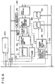
- Fig. 1 is a block diagram of an embodiment of a digital pulse processing device according to the present invention.
- a pulse processing unit 100 which has the pulse processing function according to the present invention, has the following configuration.
- a data bus 101 is used to transmit data between a microcomputer (not shown) and the pulse processing unit 100 having the pulse processing function according to the present invention.
- Clock pulses 102 are used to initiate actions within the microcomputer. They are also used to initiate actions within the pulse processing unit 100.
- Pulses from pulse generators are received by input terminals PE0A103, PE0B104, PE1A105, PE1B106, PE2A107, PE2B108.
- Input terminals PE0A103 and PE0B104 constitute channel 0
- input terminals PE1A105 and PE1B106 form channel 1
- input terminals PE2A107 and PE2B108 are channel 2. There are three channels in total.
- the pulse signal supplied to each channel is frequency multiplied and delivered to a counter PREG as a count signal by a pulse preprocessing unit 109.
- Frequency multiplication is the processing in which rise and fall of an input pulse are detected and a pulse signal is generated synchronously with the detected pulse. In this frequency multiplication processing, it is therefore possible to generate a pulse signal whose cycle is a submultiple (whose frequency is a multiple) of that of the pulse signal from the pulse generator.
- the generated pulses are supplied to counters PREG0A110, PREG0B111, PREG1A112, PREG1B113, PREG2A114 and PREG2B115 as either an counting up or down signal. Switch over between counting up and down signals is performed in accordance with the operation mode set in a mode control register MCREG129.
- Counters PREG0A110 and PREG0B111 count pulses input to the input terminals PE0A103 and PE0B104 which constitute channel 0.
- the present invention is characterized in that these two counters can be selectively used separately or in a coupled state. Coupling of the counters is conducted on the data designated by the mode control register MCREG 120.
- Counters PREG1A112 and PREG1B113 or PREG2A114 and PREG2B115 have the same function as the counters PREG0A110 and PREG0B111, and count the pulses input to the input terminals PE1A105 and PE1B106 constituting channel 1 or the input terminals PE2A107 and PE2B108 constituting channel 2.
- Coupling control circuits 117 and 118 have the same function as the coupling control circuit 117, and control separation and coupling of the counters PREG1A112 and PREG1B113, PREG2A114 and PREG2B115, respectively.
- the counted value of a timer 119 is stored in 16-bit latches. Latches TREG0A121 and TREG0B122 correspond to the counters PREG0A110 and PREG0B111. When the counters PREG0A110 and PREG0B111 are used in a coupled state, data having a double precision is obtained by the two latches TREG0A121 and TREG0B122.
- the latches TREG0A121 and TREG0B122 store the counted value of the timer 119 synchronously with the counting operation of the counters PREG0A110 and PREG0B111 which count a counting up or down signal output from the pulse preprocessing unit 109.
- Latches TREG1A123 and TREG1B124 or TREG2A125 and TREG2B126 have the same function as the latches TREG0A121 and TREG0B122, and respectively correspond to the counters PREG1A112 and PREG1B123, PREG2A114 and PREG2B115.
- Timer 119 counts the clock pulses 102 of a microcomputer which is not shown.
- the clock pulses are first divided by a value designated by the mode control register MCREG129 and then counted.
- a storing latch selecting unit 120 makes a selection of the latches TREG121 to 126 and thus determines the latch at which the data of the timer 119 is to be stored.
- the control signal sent from the pulse preprocessing unit 109 to the storing latch selecting unit 120 synchronizes counting of the pulses with latching of the timer data. This control signal is also used to indicate counting or non-counting of the counter to the storing latch selecting unit 120.
- the mode control register MCREG129 designates the operation mode of a pulse input unit 100.
- An overflow status detecting unit 127 contains a status register for memorizing that an overflow condition of the timer 119 has occurred twice or more before a subsequent reading-out of the latches TREG121 to 126. When this status register is set, disability of an accurate speed detection operation is alarmed.
- a timer latch 128 stores the value of the timer 119 when the microcomputer reads in the value in this latch 129.
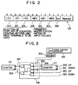
- Fig. 2 shows the bit configuration of a memory in the mode control register MCREG129.
- This register 129 has a 16-bit structure. Among the 16 bits, bits 2, 1 and 0 are not used. Bits 15 to 10 are used for making selection on the input pulses: bits 11 and 10, constituting an IP0 portion 200, are used for selecting coupling or non-coupling of the counters for counting the pulses input from the channel 0, the counting method and the input terminal to be used; bits 13 and 12, constituting an IP1 portion 201, are used for selecting coupling or non-coupling of the counters for counting the pulses input from the channel 1, the counting method and the input terminal to be used; and bits 15 and 14, constituting an IP2 portion 202, are used for selecting coupling or non-coupling of the counters for counting the pulses input from the channel 2, the counting method and the input terminal to be used.
- Allocation of the codes for the individual channels is in common and shown in Table 1.
- the counters PREGA and PREGB are not coupled but operated separately, and values are counted up in both counters. At that time, both PEA and PEB terminals are used to input pulses from the pulse output device.
- a combination of the upper and lower bits 01, the same operation is performed with the exception that values are counted down in the counters.
- the counters PREGA and PREGB are coupled, and an instruction indicating counting up or down is input to the PEA terminal while pulses are input to the PEB terminal.
- the counters PREGA and PREGB are coupled and two-phase pulses having a directional component are input to the PEA and PEB terminals. Therefore, counting up or down is performed in accordance with the directional component.
- Bits 9 to 4 are used to set the frequency multiplication factor used in the process conducted by the pulse preprocessing unit 109. That is, bits 5 and 4, constituting a MP0 portion 203, are used to set the frequency multiplication factor for the pulses input to the channel 0, bits 7 and 6, constituting a MP1 portion 204, are used to set the frequency multiplication factor for the pulses input to the channel 1, and bits 9 and 8, constituting a MP2 portion 205, are used to set the frequency multiplication factor for the pulses input to the channel 2. Examples of the frequency multiplication factors that can be set are 1, 2 and 4, as shown in Table 2.
- Bit 3 constituting a TCLK portion 206, is used to set the frequency demultiplication factor.
- 1 and 1/2 can be used as the frequency demultiplication factor, as shown in Table 3.
- Table 2 Code allocation for MP0 to 2 Upper bit Lower bit Frequency multiplication factor 0 0 x1 0 1 x2 1 0 x2 1 1 x4
- Table 3 Code allocation for TCLK Bit Frequency demultiplication factor 0 x1 0 x1/2
- Fig. 3 is a block diagram of an example of a circuit configuration which implements the counters PREG coupling function.
- coupling of the counters PREG0A110 and PREG0B111 will be described.
- An instruction indicating coupling or non-coupling of the counters PREG0A110 and PREG0B111 is set in the mode control register MCREG129. That instruction is converted into a control signal by a decoder 304.
- a carry signal 305 or a borrow signal 306 generated as a consequence of the counting operation of the counter PREG0B111 by either a counting up or down signal 300 or 301 output from the pulse preprocessing unit 109 is used as either a counting up or down signal 307 or 308 for the counter PREG0A110.
- a counting up or down signal 302 or 303 which are output from the pulse preprocessing unit 109 to the counter PREG0A110, is supplied to the counter PREG0A110 through the coupling control circuit 116 as the counting up or down signal 307 or 308 without being changed. Coupling and separation of other counters PREG are performed in the same manner.
- Fig. 4 is a block diagram of an example of a detection circuit for detecting that an overflow condition of the timer 119 has occurred twice or more in the latch TREG reading-out intervals.
- An overflow condition of the timer 119 is detected by a 32-bit carry of the counter when the counters PREG are coupled with each other and by a bit state of bit 17 when the counters PREG are separated from each other.
- Non-updated flag 402 is set by a read-out signal 400 of the microcomputer, and reset by an update signal 401 of the corresponding latch TREGA. Therefore, when the flag A402 stored in a latch 405 by the overflow signal has a value 1, it indicates that an overflow condition has occurred after the TREG is updated.
- a latch 406 stores the value of the latch 405 by the overflow signal. Consequently, logical AND between the latches OVF1A405 and OVF2A406 represents generation of an overflow condition twice or more, and the status register of the overflow status detecting unit 127 thus reflects the results of this logical operation.
- a one-shot overflow signal is generated by a one-shot circuit B408 in accordance with the bit state of bit 17. Thereafter, substantially the same operation as that regarding the latch TREGA is conducted so that a non-updating flag 407 can be set by a reading-out signal of the microcomputer 411 and an update signal 412 of the TREGB.
- Generation of an overflow condition twice or more is detected by the latches OVF1B409 and OVF2B410, and the status register of the overflow status detecting unit 127 thus reflects the results of the detection.
- the basic function of the storing latch selecting unit 120 is to store the data of the timer 119 in the latch corresponding to the counter designated by the mode control register MCREG129 each time the counter counts the input pulse. That is, the storing latch selecting unit 120 opens a latch switch in response to the count synchronizing signal sent from the pulse preprocessing unit 109 to send the data of the timer 119 to an aligner which distributes the timer data between latches 1 and 2 in accordance with the data from the mode control register MCREG129.
- Another function of the storing latch selecting unit 120 is to reduce generation of errors when no count pulse is input in the CPU's data reading out intervals, i.e., when the motor or the like is rotating at a low speed. This function is executed by a read-out signal 501 from the CPU and a signal from the timer latch (flag) 128.
- the timer latch 128 has another function. That is, although the fundamental function of the timer latch 128 is to store the data of the timer 119 when the motor or the like is rotating at a low speed, the timer latch 128 also serves as a flag used to determine whether the motor or the like is rotating at a high or low speed relative to the CPU's reading-out intervals. This flag is set by the read-out signal 501 from the CPU and is reset each time the counting operation is conducted. Therefore, the flag is in a reset state when the counting operation is conducted before a CPU's subsequent reading-out while it is in a set state when no counting operation is conducted. When the flag is in a reset state, it is therefore determined that the motor or the like is rotating at a high speed.
- the flag When the flag is in a set state, it is determined that the motor or the like is rotating at a low speed. In the latter case, the data on the timer 119 is transferred to the aligner synchronously with the reading-out signal of the CPU and then stored in the latch designated by the mode control register MCREG129.
- a wait signal 502 indicates that the data stored in the latch is not defined. This wait signal 502 is output only for a period of time corresponding to several clock pulses immediately after the latch switch is operated. The CPU confirms that no wait signal 502 is output when it reads in the timer latch 128, and then obtains the value of the timer 119.
- the microcomputer since the microcomputer reads out the counted value of the free-run counter for counting the clock pulses synchronously with the counting operation of the counter for counting the pulses of the pulse output device, burden on the software for the speed detection operation can be alleviated.
- the digital pulse processing device provided separately from the CPU has been described.
- a combination of the pulse input unit 100, serving as the digital pulse processing device according to the present invention, and a CPU 503 may be fabricated as a one-chip microcomputer.
- the counters for counting the pulses from the pulse output device are coupled with or separated from each other to change the precision of the data output from the counters, counting of a wider range can be made possible. This allows pulse processing at a precision suitable to the application to be made possible.
- the microcomputer reads out the counted value of the free-run counter for counting the clock pulses synchronously with the counting operation of the counter for counting the pulses of the pulse output device, burden on the software for the speed detection operation can be alleviated.
Landscapes
- Physics & Mathematics (AREA)
- General Physics & Mathematics (AREA)
- Manipulation Of Pulses (AREA)
- Measuring Frequencies, Analyzing Spectra (AREA)
- Control Of Electric Motors In General (AREA)
- Microcomputers (AREA)
Applications Claiming Priority (2)
| Application Number | Priority Date | Filing Date | Title |
|---|---|---|---|
| JP239742/90 | 1990-09-10 | ||
| JP2239742A JPH04121085A (ja) | 1990-09-10 | 1990-09-10 | ディジタルパルス処理装置 |
Publications (3)
| Publication Number | Publication Date |
|---|---|
| EP0476478A2 true EP0476478A2 (de) | 1992-03-25 |
| EP0476478A3 EP0476478A3 (en) | 1992-07-15 |
| EP0476478B1 EP0476478B1 (de) | 1996-02-21 |
Family
ID=17049259
Family Applications (1)
| Application Number | Title | Priority Date | Filing Date |
|---|---|---|---|
| EP91115226A Expired - Lifetime EP0476478B1 (de) | 1990-09-10 | 1991-09-09 | Digitale Impulsverarbeitungsvorrichtung |
Country Status (5)
| Country | Link |
|---|---|
| US (1) | US5289517A (de) |
| EP (1) | EP0476478B1 (de) |
| JP (1) | JPH04121085A (de) |
| KR (1) | KR100214758B1 (de) |
| DE (1) | DE69117235T2 (de) |
Cited By (5)
| Publication number | Priority date | Publication date | Assignee | Title |
|---|---|---|---|---|
| EP0576841A3 (de) * | 1992-07-01 | 1996-03-20 | Motorola, Inc. | Vorrichtung und Verfahren zur digitaler Zeitmessung |
| LT4472B (lt) | 1997-06-13 | 1999-02-25 | Akcinė Bendrovė "Elesta" | Durys, durų stakta, jų gamybos ir montavimo būdai |
| RU2224259C2 (ru) * | 2002-04-15 | 2004-02-20 | Открытое акционерное общество "Ракетно-космическая корпорация "Энергия" им. С.П.Королева" | Устройство для контроля параметров вращения |
| EP2177917A4 (de) * | 2007-09-11 | 2011-04-06 | Yaskawa Denki Seisakusho Kk | Geschwindigkeitserkennungsverfahren sowie vorrichtung zur motorensteuerung unter anwendung dieses verfahrens |
| EP2098873A3 (de) * | 2008-03-07 | 2011-12-21 | BBH Systems GmbH | Verfahren sowie Vorrichtung zur Ermittlung der Geschwindigkeit, insbesondere der Drehgeschwindigkeit eines umlaufenden Maschinenelementes |
Families Citing this family (9)
| Publication number | Priority date | Publication date | Assignee | Title |
|---|---|---|---|---|
| GB2287812B (en) * | 1994-03-24 | 1997-09-24 | Discovision Ass | Clock divider |
| JPH11219305A (ja) * | 1998-02-03 | 1999-08-10 | Mitsubishi Electric Corp | マイクロコンピュータのリセット装置及びマイクロコンピュータのリセット方法 |
| US7599287B2 (en) * | 2002-11-15 | 2009-10-06 | Cisco Technology, Inc. | Tokens in token buckets maintained among primary and secondary storages |
| US7304942B1 (en) * | 2002-11-15 | 2007-12-04 | Cisco Technology, Inc. | Methods and apparatus for maintaining statistic counters and updating a secondary counter storage via a queue for reducing or eliminating overflow of the counters |
| US8018845B2 (en) * | 2006-01-25 | 2011-09-13 | Cisco Technology, Inc | Sampling rate-limited traffic |
| US8077611B2 (en) * | 2006-07-27 | 2011-12-13 | Cisco Technology, Inc. | Multilevel coupled policer |
| DE102007010886B3 (de) * | 2007-03-06 | 2008-06-26 | Siemens Ag | Steuergerät für ein Fahrzeug |
| CN102792167B (zh) * | 2010-03-16 | 2014-09-03 | 三菱电机株式会社 | 速度检测装置 |
| CN111769822B (zh) * | 2020-06-30 | 2024-02-06 | 山东卓奇电气科技有限公司 | 频率测量装置 |
Family Cites Families (14)
| Publication number | Priority date | Publication date | Assignee | Title |
|---|---|---|---|---|
| US3832640A (en) * | 1972-12-11 | 1974-08-27 | Ford Motor Co | Time division interpolator |
| US4143327A (en) * | 1977-07-08 | 1979-03-06 | Kimball International, Inc. | Method and apparatus for generating tone signals and the like |
| US4216530A (en) * | 1978-01-10 | 1980-08-05 | Nissan Motor Company, Limited | Navigation instrument for roadway vehicles |
| FR2437741A1 (fr) * | 1978-09-26 | 1980-04-25 | Ibm France | Dispositif pour accroitre la cadence d'un train d'impulsions |
| US4277693A (en) * | 1979-11-16 | 1981-07-07 | Minnesota Mining And Manufacturing Company | Apparatus for providing a time controlled output |
| US4486890A (en) * | 1981-07-20 | 1984-12-04 | Hammes Leo R | Control arrangement for an acreage counter |
| US4501005A (en) * | 1982-05-21 | 1985-02-19 | Atlas Electronics International, Inc. | Vehicle elapsed mileage indicator |
| JPH061279B2 (ja) * | 1982-12-01 | 1994-01-05 | 株式会社日立製作所 | デイジタル式速度検出装置 |
| JPS60159657A (ja) * | 1984-01-31 | 1985-08-21 | Amada Co Ltd | 速度検出装置 |
| GB2171543B (en) * | 1985-02-27 | 1988-04-20 | Hughes Microelectronics Ltd | Counting circuit which provides for extended counter life |
| US4633183A (en) * | 1985-02-28 | 1986-12-30 | Hayes Microcomputer Products, Inc. | Constant resolution frequency synthesizer |
| DE3815535A1 (de) * | 1988-05-06 | 1989-11-16 | Heidelberger Druckmasch Ag | Verfahren und anordnung zur messung der drehzahl einer maschine |
| US5020082A (en) * | 1988-06-15 | 1991-05-28 | Seiko Epson Corporation | Asynchronous counter |
| US4912734A (en) * | 1989-02-14 | 1990-03-27 | Ail Systems, Inc. | High resolution event occurrance time counter |
-
1990
- 1990-09-10 JP JP2239742A patent/JPH04121085A/ja active Pending
-
1991
- 1991-09-09 EP EP91115226A patent/EP0476478B1/de not_active Expired - Lifetime
- 1991-09-09 DE DE69117235T patent/DE69117235T2/de not_active Expired - Fee Related
- 1991-09-10 KR KR1019910015758A patent/KR100214758B1/ko not_active Expired - Fee Related
- 1991-09-10 US US07/757,139 patent/US5289517A/en not_active Expired - Fee Related
Cited By (6)
| Publication number | Priority date | Publication date | Assignee | Title |
|---|---|---|---|---|
| EP0576841A3 (de) * | 1992-07-01 | 1996-03-20 | Motorola, Inc. | Vorrichtung und Verfahren zur digitaler Zeitmessung |
| LT4472B (lt) | 1997-06-13 | 1999-02-25 | Akcinė Bendrovė "Elesta" | Durys, durų stakta, jų gamybos ir montavimo būdai |
| RU2224259C2 (ru) * | 2002-04-15 | 2004-02-20 | Открытое акционерное общество "Ракетно-космическая корпорация "Энергия" им. С.П.Королева" | Устройство для контроля параметров вращения |
| EP2177917A4 (de) * | 2007-09-11 | 2011-04-06 | Yaskawa Denki Seisakusho Kk | Geschwindigkeitserkennungsverfahren sowie vorrichtung zur motorensteuerung unter anwendung dieses verfahrens |
| CN101784900B (zh) * | 2007-09-11 | 2012-07-18 | 株式会社安川电机 | 速度检测方法与使用该方法的马达控制装置 |
| EP2098873A3 (de) * | 2008-03-07 | 2011-12-21 | BBH Systems GmbH | Verfahren sowie Vorrichtung zur Ermittlung der Geschwindigkeit, insbesondere der Drehgeschwindigkeit eines umlaufenden Maschinenelementes |
Also Published As
| Publication number | Publication date |
|---|---|
| DE69117235D1 (de) | 1996-03-28 |
| JPH04121085A (ja) | 1992-04-22 |
| EP0476478B1 (de) | 1996-02-21 |
| US5289517A (en) | 1994-02-22 |
| KR920007349A (ko) | 1992-04-28 |
| DE69117235T2 (de) | 1996-07-04 |
| KR100214758B1 (ko) | 1999-08-02 |
| EP0476478A3 (en) | 1992-07-15 |
Similar Documents
| Publication | Publication Date | Title |
|---|---|---|
| EP0476478A2 (de) | Digitale Impulsverarbeitungsvorrichtung | |
| US4206346A (en) | System for gathering data representing the number of event occurrences | |
| US4953228A (en) | Apparatus for detecting pattern of crest line | |
| KR910004653B1 (ko) | 펄스입력장치 | |
| EP0500469B1 (de) | Synchronisationsanordnung für Demodulationsgerät und Kommunikationsverarbeitungsvorrichtung, die mit einem solchen Gerät ausgestattet ist | |
| US4958362A (en) | Clock signal generating circuit | |
| JPH0748647B2 (ja) | デューティ比判別回路 | |
| US5007056A (en) | Processing circuit having an error detecting and correcting circuit therein | |
| JP2804406B2 (ja) | パルス測定装置 | |
| JP2598547Y2 (ja) | 半導体試験装置用パターン発生器 | |
| EP0782082A2 (de) | Vorrichtung zur seriellen Datenübertragung | |
| JPH0370314A (ja) | クロック断検出回路 | |
| SU1124311A1 (ru) | Табличный сумматор по модулю три с коррекцией ошибок | |
| JPH0635998B2 (ja) | キャプチャ装置 | |
| JPS6028986Y2 (ja) | デ−タ処理装置 | |
| JPS63228006A (ja) | 光学式座標検出装置 | |
| JPS62259101A (ja) | 速度演算方式 | |
| JPH08163100A (ja) | 2計数値間差分出力方法及びその装置 | |
| JPH0750504B2 (ja) | パタ−ン認識装置 | |
| JPS59147544A (ja) | パルス計数装置 | |
| JPS60251769A (ja) | 圧縮デ−タ作成方法 | |
| JPH01320471A (ja) | リードアウトカウンタ出力読込み装置 | |
| JPS6372055A (ja) | イオン打込装置 | |
| JPS62157930A (ja) | マウスコントロ−ラ | |
| JPS61158232A (ja) | 逐次的プリアンブル信号検出回路 |
Legal Events
| Date | Code | Title | Description |
|---|---|---|---|
| PUAI | Public reference made under article 153(3) epc to a published international application that has entered the european phase |
Free format text: ORIGINAL CODE: 0009012 |
|
| AK | Designated contracting states |
Kind code of ref document: A2 Designated state(s): DE FR GB IT |
|
| PUAL | Search report despatched |
Free format text: ORIGINAL CODE: 0009013 |
|
| AK | Designated contracting states |
Kind code of ref document: A3 Designated state(s): DE FR GB IT |
|
| 17P | Request for examination filed |
Effective date: 19930115 |
|
| 17Q | First examination report despatched |
Effective date: 19940420 |
|
| GRAA | (expected) grant |
Free format text: ORIGINAL CODE: 0009210 |
|
| AK | Designated contracting states |
Kind code of ref document: B1 Designated state(s): DE FR GB IT |
|
| REF | Corresponds to: |
Ref document number: 69117235 Country of ref document: DE Date of ref document: 19960328 |
|
| ET | Fr: translation filed | ||
| ITF | It: translation for a ep patent filed | ||
| PLBE | No opposition filed within time limit |
Free format text: ORIGINAL CODE: 0009261 |
|
| STAA | Information on the status of an ep patent application or granted ep patent |
Free format text: STATUS: NO OPPOSITION FILED WITHIN TIME LIMIT |
|
| 26N | No opposition filed | ||
| PGFP | Annual fee paid to national office [announced via postgrant information from national office to epo] |
Ref country code: FR Payment date: 19990617 Year of fee payment: 9 |
|
| PGFP | Annual fee paid to national office [announced via postgrant information from national office to epo] |
Ref country code: GB Payment date: 19990625 Year of fee payment: 9 |
|
| PGFP | Annual fee paid to national office [announced via postgrant information from national office to epo] |
Ref country code: DE Payment date: 19990930 Year of fee payment: 9 |
|
| PG25 | Lapsed in a contracting state [announced via postgrant information from national office to epo] |
Ref country code: GB Free format text: LAPSE BECAUSE OF NON-PAYMENT OF DUE FEES Effective date: 20000909 |
|
| GBPC | Gb: european patent ceased through non-payment of renewal fee |
Effective date: 20000909 |
|
| PG25 | Lapsed in a contracting state [announced via postgrant information from national office to epo] |
Ref country code: FR Free format text: LAPSE BECAUSE OF NON-PAYMENT OF DUE FEES Effective date: 20010531 |
|
| PG25 | Lapsed in a contracting state [announced via postgrant information from national office to epo] |
Ref country code: DE Free format text: LAPSE BECAUSE OF NON-PAYMENT OF DUE FEES Effective date: 20010601 |
|
| REG | Reference to a national code |
Ref country code: FR Ref legal event code: ST |
|
| PG25 | Lapsed in a contracting state [announced via postgrant information from national office to epo] |
Ref country code: IT Free format text: LAPSE BECAUSE OF NON-PAYMENT OF DUE FEES Effective date: 20050909 |