EP0484321B1 - Méthode de fabrication d'un dispositif semi-conducteur à porte isolée - Google Patents
Méthode de fabrication d'un dispositif semi-conducteur à porte isolée Download PDFInfo
- Publication number
- EP0484321B1 EP0484321B1 EP92100930A EP92100930A EP0484321B1 EP 0484321 B1 EP0484321 B1 EP 0484321B1 EP 92100930 A EP92100930 A EP 92100930A EP 92100930 A EP92100930 A EP 92100930A EP 0484321 B1 EP0484321 B1 EP 0484321B1
- Authority
- EP
- European Patent Office
- Prior art keywords
- layer
- type
- insulated gate
- well regions
- side wall
- Prior art date
- Legal status (The legal status is an assumption and is not a legal conclusion. Google has not performed a legal analysis and makes no representation as to the accuracy of the status listed.)
- Expired - Lifetime
Links
Images


Classifications
-
- H—ELECTRICITY
- H10—SEMICONDUCTOR DEVICES; ELECTRIC SOLID-STATE DEVICES NOT OTHERWISE PROVIDED FOR
- H10D—INORGANIC ELECTRIC SEMICONDUCTOR DEVICES
- H10D30/00—Field-effect transistors [FET]
- H10D30/60—Insulated-gate field-effect transistors [IGFET]
- H10D30/64—Double-diffused metal-oxide semiconductor [DMOS] FETs
- H10D30/66—Vertical DMOS [VDMOS] FETs
-
- H—ELECTRICITY
- H10—SEMICONDUCTOR DEVICES; ELECTRIC SOLID-STATE DEVICES NOT OTHERWISE PROVIDED FOR
- H10D—INORGANIC ELECTRIC SEMICONDUCTOR DEVICES
- H10D12/00—Bipolar devices controlled by the field effect, e.g. insulated-gate bipolar transistors [IGBT]
- H10D12/01—Manufacture or treatment
- H10D12/031—Manufacture or treatment of IGBTs
- H10D12/032—Manufacture or treatment of IGBTs of vertical IGBTs
-
- H—ELECTRICITY
- H10—SEMICONDUCTOR DEVICES; ELECTRIC SOLID-STATE DEVICES NOT OTHERWISE PROVIDED FOR
- H10D—INORGANIC ELECTRIC SEMICONDUCTOR DEVICES
- H10D12/00—Bipolar devices controlled by the field effect, e.g. insulated-gate bipolar transistors [IGBT]
- H10D12/411—Insulated-gate bipolar transistors [IGBT]
- H10D12/441—Vertical IGBTs
-
- H—ELECTRICITY
- H10—SEMICONDUCTOR DEVICES; ELECTRIC SOLID-STATE DEVICES NOT OTHERWISE PROVIDED FOR
- H10D—INORGANIC ELECTRIC SEMICONDUCTOR DEVICES
- H10D30/00—Field-effect transistors [FET]
- H10D30/01—Manufacture or treatment
- H10D30/021—Manufacture or treatment of FETs having insulated gates [IGFET]
- H10D30/028—Manufacture or treatment of FETs having insulated gates [IGFET] of double-diffused metal oxide semiconductor [DMOS] FETs
- H10D30/0291—Manufacture or treatment of FETs having insulated gates [IGFET] of double-diffused metal oxide semiconductor [DMOS] FETs of vertical DMOS [VDMOS] FETs
-
- H—ELECTRICITY
- H10—SEMICONDUCTOR DEVICES; ELECTRIC SOLID-STATE DEVICES NOT OTHERWISE PROVIDED FOR
- H10P—GENERIC PROCESSES OR APPARATUS FOR THE MANUFACTURE OR TREATMENT OF DEVICES COVERED BY CLASS H10
- H10P32/00—Diffusion of dopants within, into or out of wafers, substrates or parts of devices
- H10P32/10—Diffusion of dopants within, into or out of semiconductor bodies or layers
- H10P32/14—Diffusion of dopants within, into or out of semiconductor bodies or layers within a single semiconductor body or layer in a solid phase; between different semiconductor bodies or layers, both in a solid phase
- H10P32/1408—Diffusion of dopants within, into or out of semiconductor bodies or layers within a single semiconductor body or layer in a solid phase; between different semiconductor bodies or layers, both in a solid phase from or through or into an external applied layer, e.g. photoresist or nitride layers
- H10P32/1414—Diffusion of dopants within, into or out of semiconductor bodies or layers within a single semiconductor body or layer in a solid phase; between different semiconductor bodies or layers, both in a solid phase from or through or into an external applied layer, e.g. photoresist or nitride layers the applied layer being silicon, silicide or SIPOS, e.g. polysilicon or porous silicon
-
- H—ELECTRICITY
- H10—SEMICONDUCTOR DEVICES; ELECTRIC SOLID-STATE DEVICES NOT OTHERWISE PROVIDED FOR
- H10P—GENERIC PROCESSES OR APPARATUS FOR THE MANUFACTURE OR TREATMENT OF DEVICES COVERED BY CLASS H10
- H10P32/00—Diffusion of dopants within, into or out of wafers, substrates or parts of devices
- H10P32/10—Diffusion of dopants within, into or out of semiconductor bodies or layers
- H10P32/17—Diffusion of dopants within, into or out of semiconductor bodies or layers characterised by the semiconductor material
- H10P32/171—Diffusion of dopants within, into or out of semiconductor bodies or layers characterised by the semiconductor material being group IV material
-
- Y—GENERAL TAGGING OF NEW TECHNOLOGICAL DEVELOPMENTS; GENERAL TAGGING OF CROSS-SECTIONAL TECHNOLOGIES SPANNING OVER SEVERAL SECTIONS OF THE IPC; TECHNICAL SUBJECTS COVERED BY FORMER USPC CROSS-REFERENCE ART COLLECTIONS [XRACs] AND DIGESTS
- Y10—TECHNICAL SUBJECTS COVERED BY FORMER USPC
- Y10S—TECHNICAL SUBJECTS COVERED BY FORMER USPC CROSS-REFERENCE ART COLLECTIONS [XRACs] AND DIGESTS
- Y10S148/00—Metal treatment
- Y10S148/126—Power FETs
Definitions
- the present invention relates to a method of fabricating a semiconductor device having an insulated gate (hereinafter referred to as an insulated gate semiconductor device) and more particularly to a method for fabricating such a device as is suitable to provide a high current density.
- an insulated gate semiconductor device hereinafter referred to as an insulated gate semiconductor device
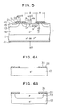
- the semiconductor device to which the present invention relates has such a structure as shown in Fig. 5.
- 11 is an n + -type or p + -type semiconductor substrate
- 12 is an n - -type layer formed on the semiconductor substrate 11 and having a higher resistivity than the semiconductor substrate 11
- 13 are a plurality of p + -type wells which extend into the n - -type layer 12 from the surface thereof on the side opposite to the side adjacent to the semiconductor substrate 11
- 15 are n + -type sources which extend into the p + -well 13 from the surface thereof
- 31 are gate electrodes each formed on the exposed portions of the n - -type layer 12 and p-type well 13 adjacent thereto through a gate oxide film 21
- 22 are insulating films each formed so as to cover the gate electrode 31 and a part of the n + -type source layer 15 adjacent thereto
- 41 is a drain electrode kept in ohmic contact with the surface of the semiconductor substrate 11 on the side opposite to the side adjacent
- the semiconductor device as shown is an unipolar device commonly called "MOSFET" in the case where the semiconductor substrate 11 is of n + -type.
- MOSFET unipolar device commonly called "MOSFET" in the case where the semiconductor substrate 11 is of n + -type.
- the n - -type layer 12 which has been of a higher resistivity exhibits a conductivity of lower resistivity.
- that semiconductor device is called "conductivity modulated MOSFET", in which the electrons serve as a base current and a pnp transistor consisting of the p + -type substrate 11, the n - -type layer 12 and the p-type well layer 13 is operated.
- the injected holes flow into the source electrode 42 through the p-type well layer 13 under the n + -type source layer 15.
- the potential applied to the gate electrode 31 is removed as in the case of the unipolar MOSFET. Then, the path of electrons ⁇ is cut off so that the base current of the pnp transistor is not supplied. Thus, the holes are not injected whereby the current does not flow.
- a n + -type or p + -type semiconductor substrate 11 is prepared and an n - -type 12 is formed on one surface thereof.
- a stack (insulated gate) of a gate oxide film 21 and a gate electrode 31 are selectively formed on the surface of the n - -type layer 12 on the side opposite to the side adjacent to the semiconductor substrate 11 (Fig. 6A).
- boron (B) is ion-implanted in the surface of the n - -type layer 12 where no mask is located thereon, and the substrate is heat-treated to from a p-type well layer 13 (Fig.
- a resist film 29 is formed on the p-type well layer 13 surface at the selected location thereof. Using, as a mask, this resist film and the stack of the gate oxide film 21 and the gate electrode 31, arsenic (As) or phosphorus (P) is ion-implanted in the p-type well layer 13 surface at the location where the mask is not present, (Fig. 6C). After the ion-implantation, the resist film 29 is removed and the substrate is heat-treated to form n + -type source layers 15 (Fig. 6D). An insulating film 22 is formed on the stack consisting of the gate oxide film 21 and the gate electrode 31 and on the exposed portions of the p-type well layer 13 and the n + -type source layer 15 (Fig. 6E).
- a portion of the insulating film 22 located on portions of the n + -type source layers and a portion of the p-type well layer 13 exposed between the n + -layer source layers 15 is selectively removed and a source electrode 42 is formed on the remaining insulating film 22 and on the portions of the n + -type source layers 15 and the p-type well layer 13 exposed by removing the portion of the insulating film 22 (Fig. 6F).
- the insulating gate semiconductor device fabricated by the process as mentioned above has a disadvantage that it can not provide a high current density.
- the current density of the semiconductor device having insulated gate as shown in Fig. 5 can be enhanced by providing a larger percentage area occupied by the gate region B in a device unit and a smaller percentage area occupied by the remaining region A.
- the area of the region A can not be decreased for the following reason.
- size A 1 of the insulating film 22 required to insulate the gate electrode 31 from the source electrode 42, size A 2 required to surely bring the source electrode 42 and the n + -type layers 15 into contact with each other, and size A 3 required to separate the n + -type layers 15 from each other and bring the p-type layer 13 and the source electrode 42 into contact with each other, which depends on the processing accuracy of the resist film 29, are required to be at least 3 ⁇ m. Since these sizes must take some allowance considering the safety rates, the entire width (2A 1 + 2A 2 + A 3 ) of the region A reaches 20 to 30 ⁇ m, which will occupy 50 % of the device unit. Thus, the percentage of the gate region B can not be further increased, which makes it impossible to enhance the current density.
- n + -type source layer 15 In the case of a conductivity modulated MOSFET using a p + -type substrate, if the width (A 1 + A 2 ) of the n + -type source layer 15 is too large, injected holes ⁇ produce a voltage drop in the p-type well layer 13 due to the lateral resistance R in the p-type well layer 13 under the n + -type layer 15, thereby forward biasing the n + -type source layer 15 and the p-type well layer 13. Thus, an npn transistor consisting of the n + -type source layer 15, the p-type well layer 13 and the n - -type layer 12 is started to operate, thus injecting electrons into the p-type well layer 13 from the n + -type source layer 15.
- EP-A-0 179 407 discloses a method of fabricating a DMOS device, comprising the steps of forming selectively two-layer structures on a semiconductor layer of one conductivity type, the two-layer structure consisting of an insulating layer and a gate electrode; forming well layers of the other conductivity type using the two-layer structures as masks; covering a central part of the well layer by an insulating layer, and then forming a polysilicon layer doped with impurities on totally an exposed portion of the well layers, the two-layer structures and the insulating layer; diffusing the impurities of one conductivity type from the polysilicon layer to form source layers in the well layers; covering the two-layer structures by SiO 2 films and forming source electrodes.
- EP-A-0 083 785 discloses a method of fabricating FET structures, comprising the steps of forming selectively two-layer structures on a P-type substrate, the structure consisting of an N + type polysilicon layer and a SiO 2 layer; forming a SiO 2 film doped with impurities of N-type on side walls of the two-layer structures; diffusing the impurities from the polysilicon layer and the SiO 2 into the substrate to form source layers and drain layers; forming insulating gates between the two-layer structures.
- Another object of the present invention is to provide a method for fabricating an insulated gate semiconductor device having a high current density with high accuracy.
- Still another object of the present invention is to provide a method for fabricating an insulated gate semiconductor device with a larger percentage of the area occupied by a gate region in a device unit.
- a further object of the present invention is to provide an insulated gate semiconductor device with reduced parasitic bipolar transistor effect.
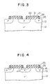
- Figs. 1 to 4 show a typical embodiment of the present invention, which comprises the following steps
- the heat treatment is performed at the temperature of approximately 1000°C for the period which is decided in accordance with the selected depth of the n + -type source layers 15.
- a source electrode is formed on the stacks, the remaining films 26 and the exposed surface of the n + -type source layers 15 and the p-type well layers 13.
- the undoped insulating film 25 is located between the gate electrode 31 and the source electrode so that both electrodes can be surely insulated from each other.
- the doped film 26 which serves as a diffusion source 15 for the n + -type source layer 15 is not required to be electrically insulative so that the conductor such as doped poly-silicon can be used, which assures that the n + -type source layers 15 and the source electrode are kept in contact with each other.
- the present invention can also provide the same effects when it is a p-channel MOSFET.
Landscapes
- Metal-Oxide And Bipolar Metal-Oxide Semiconductor Integrated Circuits (AREA)
- Insulated Gate Type Field-Effect Transistor (AREA)
- Bipolar Transistors (AREA)
Claims (2)
- Procédé de fabrication d'un transistor à grille isolée verticalement comportant:une couche semiconductrice d'un premier type de conductivité;une pluralité de régions de puits (13) d'un deuxième type de conductivité opposé audit premier type de conductivité, formées de manière espacée l'une de l'autre et lesdites régions de puits ayant des surfaces exposées sur une face de ladite couche semiconductrice (12);des régions de source (15) dudit premier type de conductivité, deux de celles-ci étant formées dans chacune desdites régions de puits et lesdites régions de source ayant des surfaces exposées sur ladite face de ladite couche semiconductrice;des empilements de grilles isolées constitués par trois couches, une couche (21) d'oxyde de grille sur ladite face de ladite couche semiconductrice, une couche formant électrode de grille (31) sur ladite couche d'oxyde de grille, etune couche isolante (22) sur ladite couche formant électrode de grille (31);et une électrode de source (42) au contact de parties desdites surfaces exposées des régions de puits (13) et desdites régions de source (15) et s'étendant sur lesdits empilements de grilles isolées,comprenant les étapes consistant à:former lesdits empilements de grilles isolées sur ladite face de ladite couche semiconductrice (12);former lesdites régions de puits (13) en introduisant des impuretés dudit deuxième type de conductivité dans ladite couche semiconductrice (12) en utilisant comme masques lesdits empilements de grilles isolées;former un film d'isolant non dopé (25) sur toute la surface de la structure réalisée et effectuer une attaque anisotrope à sec dudit film d'isolant non dopé (25), de façon que seules des parties de parois latérales de celui-ci soient laissées sur les parois latérales desdits empilements de grilles isolées et que les autres parties de celui-ci soient entièrement éliminées, pour former de ce fait des parties (25) de parois latérales du film d'isolant non dopé sur lesdites parois latérales desdits empilements de grilles isolées, au contact de la couche (21) d'oxyde de grille, de la couche formant électrode de grille (31), de la couche isolante (22) et, partiellement, des parties exposées desdites régions de puits ;former un film dopé (26), dopé avec des impuretés dudit premier type de conductivité sur toute la surface de la structure réalisée, et effectuer une attaque anisotrope à sec dudit film dopé (26), de façon que seules des parties de parois latérales de celui-ci soient laissées sur lesdites parties de parois latérales dudit d'isolant non dopé et que les autres parties de celui-ci soient entièrement éliminées, pour former de ce fait des parties (26) de parois latérales du film dopé au contact desdites parties (25) de parois latérales du film d'isolant et, partiellement, des parties exposées desdites régions de puits ;faire diffuser lesdites impuretés depuis lesdites parties (26) de parois latérales du film dopé jusqu'auxdites régions de puits (13) afin de former lesdites régions de source (15), etformer ladite électrode de source (42) maintenue en contact ohmique avec les parties exposées des deux régions de source correspondantes (15) dans une seule desdites régions de puits, et desdites régions de puits (13), s'étendant sur deux empilements de grilles isolées correspondants, et isolée desdites couches formant électrodes de grilles (31) par lesdites parties (25) de parois latérales du film d'isolant.
- Procédé selon la revendication 1, dans lequel
ledit film dopé (26) est en silicium polycristallin dopé avec lesdites impuretés dudit premier type de conductivité.
Applications Claiming Priority (3)
| Application Number | Priority Date | Filing Date | Title |
|---|---|---|---|
| JP208123/87 | 1987-08-24 | ||
| JP62208123A JPH0766968B2 (ja) | 1987-08-24 | 1987-08-24 | 半導体装置及びその製造方法 |
| EP88113602A EP0304839B1 (fr) | 1987-08-24 | 1988-08-22 | Méthode de fabrication d'un dispositif semi-conducteur à porte isolée |
Related Parent Applications (2)
| Application Number | Title | Priority Date | Filing Date |
|---|---|---|---|
| EP88113602.2 Division | 1988-08-22 | ||
| EP88113602A Division EP0304839B1 (fr) | 1987-08-24 | 1988-08-22 | Méthode de fabrication d'un dispositif semi-conducteur à porte isolée |
Publications (2)
| Publication Number | Publication Date |
|---|---|
| EP0484321A1 EP0484321A1 (fr) | 1992-05-06 |
| EP0484321B1 true EP0484321B1 (fr) | 1997-12-10 |
Family
ID=16551016
Family Applications (4)
| Application Number | Title | Priority Date | Filing Date |
|---|---|---|---|
| EP01125303A Withdrawn EP1191600A3 (fr) | 1987-08-24 | 1988-08-22 | Dispositif semi-conducteur à grille isolée |
| EP94101050A Expired - Lifetime EP0604392B1 (fr) | 1987-08-24 | 1988-08-22 | Dispositif semi-conducteur à porte isolée |
| EP92100930A Expired - Lifetime EP0484321B1 (fr) | 1987-08-24 | 1988-08-22 | Méthode de fabrication d'un dispositif semi-conducteur à porte isolée |
| EP88113602A Expired - Lifetime EP0304839B1 (fr) | 1987-08-24 | 1988-08-22 | Méthode de fabrication d'un dispositif semi-conducteur à porte isolée |
Family Applications Before (2)
| Application Number | Title | Priority Date | Filing Date |
|---|---|---|---|
| EP01125303A Withdrawn EP1191600A3 (fr) | 1987-08-24 | 1988-08-22 | Dispositif semi-conducteur à grille isolée |
| EP94101050A Expired - Lifetime EP0604392B1 (fr) | 1987-08-24 | 1988-08-22 | Dispositif semi-conducteur à porte isolée |
Family Applications After (1)
| Application Number | Title | Priority Date | Filing Date |
|---|---|---|---|
| EP88113602A Expired - Lifetime EP0304839B1 (fr) | 1987-08-24 | 1988-08-22 | Méthode de fabrication d'un dispositif semi-conducteur à porte isolée |
Country Status (4)
| Country | Link |
|---|---|
| US (1) | US5032532A (fr) |
| EP (4) | EP1191600A3 (fr) |
| JP (1) | JPH0766968B2 (fr) |
| DE (3) | DE3856545T2 (fr) |
Families Citing this family (32)
| Publication number | Priority date | Publication date | Assignee | Title |
|---|---|---|---|---|
| KR920003320B1 (ko) * | 1988-03-05 | 1992-04-27 | 한국과학 기술원 | 매우 작은 소오스 영역을 갖는 자기 정렬된 수직 이중 확산형 전력 mosfet의 제조방법 |
| US5342797A (en) * | 1988-10-03 | 1994-08-30 | National Semiconductor Corporation | Method for forming a vertical power MOSFET having doped oxide side wall spacers |
| JP2689606B2 (ja) * | 1989-05-24 | 1997-12-10 | 富士電機株式会社 | 絶縁ゲート電界効果型トランジスタの製造方法 |
| US5262339A (en) * | 1989-06-12 | 1993-11-16 | Hitachi, Ltd. | Method of manufacturing a power semiconductor device using implants and solid diffusion source |
| JPH03105978A (ja) * | 1989-09-20 | 1991-05-02 | Hitachi Ltd | 半導体装置 |
| JP2598328B2 (ja) * | 1989-10-17 | 1997-04-09 | 三菱電機株式会社 | 半導体装置およびその製造方法 |
| US5171699A (en) * | 1990-10-03 | 1992-12-15 | Texas Instruments Incorporated | Vertical DMOS transistor structure built in an N-well CMOS-based BiCMOS process and method of fabrication |
| US5273934A (en) * | 1991-06-19 | 1993-12-28 | Siemens Aktiengesellschaft | Method for producing a doped region in a substrate |
| US5182222A (en) * | 1991-06-26 | 1993-01-26 | Texas Instruments Incorporated | Process for manufacturing a DMOS transistor |
| JPH05218436A (ja) * | 1992-02-03 | 1993-08-27 | Nec Corp | Pチャネル縦型mos電界効果トランジスタ |
| JPH05226352A (ja) * | 1992-02-17 | 1993-09-03 | Mitsubishi Electric Corp | 半導体装置及びその製造方法 |
| US5753530A (en) * | 1992-04-21 | 1998-05-19 | Seiko Instruments, Inc. | Impurity doping method with diffusion source of boron-silicide film |
| US5449886A (en) * | 1993-03-09 | 1995-09-12 | University Of Cincinnati | Electric heating element assembly |
| US5369045A (en) * | 1993-07-01 | 1994-11-29 | Texas Instruments Incorporated | Method for forming a self-aligned lateral DMOS transistor |
| JP3186421B2 (ja) * | 1994-05-13 | 2001-07-11 | 富士電機株式会社 | 半導体装置の製造方法 |
| US5739061A (en) * | 1993-10-26 | 1998-04-14 | Fuji Electric Co., Ltd. | Method of manufacturing a semiconductor device using gate side wall as mask for self-alignment |
| EP0689238B1 (fr) * | 1994-06-23 | 2002-02-20 | STMicroelectronics S.r.l. | Procédé de manufacture d'un dispositif de puissance en technologie MOS |
| US5817546A (en) * | 1994-06-23 | 1998-10-06 | Stmicroelectronics S.R.L. | Process of making a MOS-technology power device |
| DE69428894T2 (de) * | 1994-08-02 | 2002-04-25 | Consorzio Per La Ricerca Sulla Microelettronica Nel Mezzogiorno, Catania | Bipolartransistor mit isolierter Steuerelektrode |
| US5798554A (en) * | 1995-02-24 | 1998-08-25 | Consorzio Per La Ricerca Sulla Microelettronica Nel Mezzogiorno | MOS-technology power device integrated structure and manufacturing process thereof |
| US5518945A (en) * | 1995-05-05 | 1996-05-21 | International Business Machines Corporation | Method of making a diffused lightly doped drain device with built in etch stop |
| US5591650A (en) * | 1995-06-08 | 1997-01-07 | Taiwan Semiconductor Manufacturing Company Ltd. | Method of making a body contacted SOI MOSFET |
| DE69531783T2 (de) * | 1995-10-09 | 2004-07-15 | Consorzio Per La Ricerca Sulla Microelettronica Nel Mezzogiorno - Corimme | Herstellungsverfahren für Leistungsanordnung mit Schutzring |
| EP0772241B1 (fr) | 1995-10-30 | 2004-06-09 | STMicroelectronics S.r.l. | Dispositif de puissance à haute densité en technologie MOS |
| EP0772242B1 (fr) | 1995-10-30 | 2006-04-05 | STMicroelectronics S.r.l. | Dispositif de puissance en technologie MOS avec une seule dimension critique |
| EP0772244B1 (fr) * | 1995-11-06 | 2000-03-22 | Consorzio per la Ricerca sulla Microelettronica nel Mezzogiorno | Dispositif de puissance en technologie MOS avec résistance de sortie et capacité faibles et son procédé de fabrication |
| US6228719B1 (en) | 1995-11-06 | 2001-05-08 | Stmicroelectronics S.R.L. | MOS technology power device with low output resistance and low capacitance, and related manufacturing process |
| DE69518653T2 (de) * | 1995-12-28 | 2001-04-19 | Consorzio Per La Ricerca Sulla Microelettronica Nel Mezzogiorno, Catania | MOS-Technologie-Leistungsanordnung in integrierter Struktur |
| US5877044A (en) * | 1997-03-11 | 1999-03-02 | Harris Corporation | Method of making MOS-gated semiconductor devices |
| EP0961325B1 (fr) | 1998-05-26 | 2008-05-07 | STMicroelectronics S.r.l. | Dispositif de puissance en technologie MOS à haute densité d'intégration |
| JP5025935B2 (ja) * | 2005-09-29 | 2012-09-12 | オンセミコンダクター・トレーディング・リミテッド | 絶縁ゲート型電界効果トランジスタの製造方法 |
| JP2016029707A (ja) * | 2014-07-24 | 2016-03-03 | 住友電気工業株式会社 | 炭化珪素半導体装置 |
Family Cites Families (30)
| Publication number | Priority date | Publication date | Assignee | Title |
|---|---|---|---|---|
| US3907617A (en) * | 1971-10-22 | 1975-09-23 | Motorola Inc | Manufacture of a high voltage Schottky barrier device |
| US4209350A (en) * | 1978-11-03 | 1980-06-24 | International Business Machines Corporation | Method for forming diffusions having narrow dimensions utilizing reactive ion etching |
| US4364073A (en) * | 1980-03-25 | 1982-12-14 | Rca Corporation | Power MOSFET with an anode region |
| US4691435A (en) * | 1981-05-13 | 1987-09-08 | International Business Machines Corporation | Method for making Schottky diode having limited area self-aligned guard ring |
| JPS58115859A (ja) * | 1981-12-28 | 1983-07-09 | Fujitsu Ltd | 半導体装置の製造方法 |
| US4419809A (en) * | 1981-12-30 | 1983-12-13 | International Business Machines Corporation | Fabrication process of sub-micrometer channel length MOSFETs |
| US4445267A (en) * | 1981-12-30 | 1984-05-01 | International Business Machines Corporation | MOSFET Structure and process to form micrometer long source/drain spacing |
| US4419810A (en) * | 1981-12-30 | 1983-12-13 | International Business Machines Corporation | Self-aligned field effect transistor process |
| NL8105920A (nl) * | 1981-12-31 | 1983-07-18 | Philips Nv | Halfgeleiderinrichting en werkwijze voor het vervaardigen van een dergelijke halfgeleiderinrichting. |
| US4598461A (en) * | 1982-01-04 | 1986-07-08 | General Electric Company | Methods of making self-aligned power MOSFET with integral source-base short |
| US4503598A (en) * | 1982-05-20 | 1985-03-12 | Fairchild Camera & Instrument Corporation | Method of fabricating power MOSFET structure utilizing self-aligned diffusion and etching techniques |
| US4466176A (en) * | 1982-08-09 | 1984-08-21 | General Electric Company | Process for manufacturing insulated-gate semiconductor devices with integral shorts |
| US4417385A (en) * | 1982-08-09 | 1983-11-29 | General Electric Company | Processes for manufacturing insulated-gate semiconductor devices with integral shorts |
| US4546535A (en) * | 1983-12-12 | 1985-10-15 | International Business Machines Corporation | Method of making submicron FET structure |
| US4587713A (en) * | 1984-02-22 | 1986-05-13 | Rca Corporation | Method for making vertical MOSFET with reduced bipolar effects |
| JPS6197973A (ja) * | 1984-10-19 | 1986-05-16 | Matsushita Electronics Corp | Mosfetの製造方法 |
| IT1213234B (it) * | 1984-10-25 | 1989-12-14 | Sgs Thomson Microelectronics | Procedimento perfezionato per la fabbricazione di dispositivi a semiconduttore dmos. |
| JPS61156883A (ja) * | 1984-12-28 | 1986-07-16 | Toshiba Corp | 半導体装置の製造方法 |
| JPS61156882A (ja) * | 1984-12-28 | 1986-07-16 | Toshiba Corp | 二重拡散形絶縁ゲ−ト電界効果トランジスタ及びその製造方法 |
| US4639754A (en) * | 1985-02-25 | 1987-01-27 | Rca Corporation | Vertical MOSFET with diminished bipolar effects |
| EP0202477A3 (fr) * | 1985-04-24 | 1988-04-20 | General Electric Company | Procédé pour former des courts-circuits électriques entre des régions voisines dans un dispositif semi-conducteur à gâchette isolée |
| JPS6246568A (ja) * | 1985-08-23 | 1987-02-28 | Tdk Corp | 縦形半導体装置の製造方法 |
| JPS6246570A (ja) * | 1985-08-23 | 1987-02-28 | Tdk Corp | 縦形半導体装置及びその製造方法 |
| US4809045A (en) * | 1985-09-30 | 1989-02-28 | General Electric Company | Insulated gate device |
| GB8527062D0 (en) * | 1985-11-02 | 1985-12-04 | Plessey Co Plc | Mos transistor manufacture |
| JPS62132366A (ja) * | 1985-12-04 | 1987-06-15 | Nec Corp | 縦型電界効果トランジスタの製造方法 |
| IT1204243B (it) * | 1986-03-06 | 1989-03-01 | Sgs Microelettronica Spa | Procedimento autoallineato per la fabbricazione di celle dmos di piccole dimensioni e dispositivi mos ottenuti mediante detto procedimento |
| US4775879A (en) * | 1987-03-18 | 1988-10-04 | Motorola Inc. | FET structure arrangement having low on resistance |
| JPH0766966B2 (ja) * | 1987-04-06 | 1995-07-19 | 株式会社日立製作所 | 半導体装置 |
| JPH06246568A (ja) * | 1993-02-26 | 1994-09-06 | Okuma Mach Works Ltd | 自動工具交換中の異常監視方法 |
-
1987
- 1987-08-24 JP JP62208123A patent/JPH0766968B2/ja not_active Expired - Lifetime
-
1988
- 1988-08-17 US US07/233,007 patent/US5032532A/en not_active Expired - Lifetime
- 1988-08-22 EP EP01125303A patent/EP1191600A3/fr not_active Withdrawn
- 1988-08-22 DE DE3856545T patent/DE3856545T2/de not_active Expired - Lifetime
- 1988-08-22 DE DE3852444T patent/DE3852444T2/de not_active Expired - Lifetime
- 1988-08-22 EP EP94101050A patent/EP0604392B1/fr not_active Expired - Lifetime
- 1988-08-22 EP EP92100930A patent/EP0484321B1/fr not_active Expired - Lifetime
- 1988-08-22 EP EP88113602A patent/EP0304839B1/fr not_active Expired - Lifetime
- 1988-08-22 DE DE3856084T patent/DE3856084T2/de not_active Expired - Lifetime
Also Published As
| Publication number | Publication date |
|---|---|
| DE3856545D1 (de) | 2002-12-19 |
| US5032532A (en) | 1991-07-16 |
| EP0604392A1 (fr) | 1994-06-29 |
| EP0304839A3 (en) | 1989-08-30 |
| DE3852444T2 (de) | 1995-05-04 |
| EP0304839B1 (fr) | 1994-12-14 |
| DE3856084T2 (de) | 1998-08-27 |
| JPH0766968B2 (ja) | 1995-07-19 |
| DE3856084D1 (de) | 1998-01-22 |
| JPS6451665A (en) | 1989-02-27 |
| DE3856545T2 (de) | 2003-12-11 |
| DE3852444D1 (de) | 1995-01-26 |
| EP0484321A1 (fr) | 1992-05-06 |
| EP0304839A2 (fr) | 1989-03-01 |
| EP1191600A2 (fr) | 2002-03-27 |
| EP0604392B1 (fr) | 2002-11-13 |
| EP1191600A3 (fr) | 2002-07-31 |
Similar Documents
| Publication | Publication Date | Title |
|---|---|---|
| EP0484321B1 (fr) | Méthode de fabrication d'un dispositif semi-conducteur à porte isolée | |
| US4803176A (en) | Integrated circuit structure with active device in merged slot and method of making same | |
| US5420061A (en) | Method for improving latchup immunity in a dual-polysilicon gate process | |
| EP0186855B1 (fr) | Dispositif semi-conducteur de mémoire morte et méthode de fabrication | |
| EP0318297B1 (fr) | Dispositif semi-conducteur avec un transistor à effet de champ ayant une diode protectrice entre source et drain | |
| JP3455452B2 (ja) | 半導体デバイス及びその製造方法 | |
| US5721148A (en) | Method for manufacturing MOS type semiconductor device | |
| KR0175276B1 (ko) | 전력반도체장치 및 그의 제조방법 | |
| EP0091686B1 (fr) | Dispositif semi-conducteur ayant une région diffusée à longueur réduite et procédé pour la fabrication de la région | |
| US5179034A (en) | Method for fabricating insulated gate semiconductor device | |
| JPS60253275A (ja) | 高密度v溝型mos制御型サイリスタ、絶縁ゲ−ト型トランジスタおよびmosfet、並びに製造方法 | |
| US4567641A (en) | Method of fabricating semiconductor devices having a diffused region of reduced length | |
| US5285094A (en) | Vertical insulated gate semiconductor device with less influence from the parasitic bipolar effect | |
| US6440788B2 (en) | Implant sequence for multi-function semiconductor structure and method | |
| KR900007048B1 (ko) | 종형 mos 반도체장치 | |
| JPH07122657A (ja) | 半導体メモリとその製法 | |
| EP0034341B1 (fr) | Procédé de fabrication d'un dispositif semiconducteur | |
| KR920010962A (ko) | 반도체 디바이스 및 그 형성 방법 | |
| EP0401577B1 (fr) | Dispositif semi-conducteur métal-oxyde et sa méthode de fabrication | |
| US5143859A (en) | Method of manufacturing a static induction type switching device | |
| JP2508826B2 (ja) | 半導体装置 | |
| JPH0766966B2 (ja) | 半導体装置 | |
| EP0360998B1 (fr) | Dispositif semi-conducteur dont la surface d'isolation des éléments est modifiée | |
| JP2519541B2 (ja) | 半導体装置 | |
| US5264381A (en) | Method of manufacturing a static induction type switching device |
Legal Events
| Date | Code | Title | Description |
|---|---|---|---|
| PUAI | Public reference made under article 153(3) epc to a published international application that has entered the european phase |
Free format text: ORIGINAL CODE: 0009012 |
|
| AC | Divisional application: reference to earlier application |
Ref document number: 304839 Country of ref document: EP |
|
| AK | Designated contracting states |
Kind code of ref document: A1 Designated state(s): CH DE FR GB LI NL SE |
|
| 17P | Request for examination filed |
Effective date: 19920318 |
|
| 17Q | First examination report despatched |
Effective date: 19950510 |
|
| GRAG | Despatch of communication of intention to grant |
Free format text: ORIGINAL CODE: EPIDOS AGRA |
|
| GRAG | Despatch of communication of intention to grant |
Free format text: ORIGINAL CODE: EPIDOS AGRA |
|
| GRAH | Despatch of communication of intention to grant a patent |
Free format text: ORIGINAL CODE: EPIDOS IGRA |
|
| GRAH | Despatch of communication of intention to grant a patent |
Free format text: ORIGINAL CODE: EPIDOS IGRA |
|
| GRAA | (expected) grant |
Free format text: ORIGINAL CODE: 0009210 |
|
| RBV | Designated contracting states (corrected) |
Designated state(s): DE FR GB |
|
| AC | Divisional application: reference to earlier application |
Ref document number: 304839 Country of ref document: EP |
|
| AK | Designated contracting states |
Kind code of ref document: B1 Designated state(s): DE FR GB |
|
| REF | Corresponds to: |
Ref document number: 3856084 Country of ref document: DE Date of ref document: 19980122 |
|
| ET | Fr: translation filed | ||
| PLBE | No opposition filed within time limit |
Free format text: ORIGINAL CODE: 0009261 |
|
| STAA | Information on the status of an ep patent application or granted ep patent |
Free format text: STATUS: NO OPPOSITION FILED WITHIN TIME LIMIT |
|
| 26N | No opposition filed | ||
| REG | Reference to a national code |
Ref country code: GB Ref legal event code: IF02 |
|
| PGFP | Annual fee paid to national office [announced via postgrant information from national office to epo] |
Ref country code: GB Payment date: 20050801 Year of fee payment: 18 |
|
| GBPC | Gb: european patent ceased through non-payment of renewal fee |
Effective date: 20060822 |
|
| PGFP | Annual fee paid to national office [announced via postgrant information from national office to epo] |
Ref country code: DE Payment date: 20070907 Year of fee payment: 20 |
|
| PG25 | Lapsed in a contracting state [announced via postgrant information from national office to epo] |
Ref country code: GB Free format text: LAPSE BECAUSE OF NON-PAYMENT OF DUE FEES Effective date: 20060822 |
|
| PGFP | Annual fee paid to national office [announced via postgrant information from national office to epo] |
Ref country code: FR Payment date: 20070712 Year of fee payment: 20 |