EP0692826A2 - Méthode pour supprimer des fuites sous-seuils à cause de coins d'isolation acérés dans des structures FET submicroniques - Google Patents
Méthode pour supprimer des fuites sous-seuils à cause de coins d'isolation acérés dans des structures FET submicroniques Download PDFInfo
- Publication number
- EP0692826A2 EP0692826A2 EP95480073A EP95480073A EP0692826A2 EP 0692826 A2 EP0692826 A2 EP 0692826A2 EP 95480073 A EP95480073 A EP 95480073A EP 95480073 A EP95480073 A EP 95480073A EP 0692826 A2 EP0692826 A2 EP 0692826A2
- Authority
- EP
- European Patent Office
- Prior art keywords
- length
- shallow trench
- phase shift
- gate
- mask
- Prior art date
- Legal status (The legal status is an assumption and is not a legal conclusion. Google has not performed a legal analysis and makes no representation as to the accuracy of the status listed.)
- Withdrawn
Links
Images


Classifications
-
- H—ELECTRICITY
- H10—SEMICONDUCTOR DEVICES; ELECTRIC SOLID-STATE DEVICES NOT OTHERWISE PROVIDED FOR
- H10D—INORGANIC ELECTRIC SEMICONDUCTOR DEVICES
- H10D30/00—Field-effect transistors [FET]
- H10D30/01—Manufacture or treatment
- H10D30/021—Manufacture or treatment of FETs having insulated gates [IGFET]
- H10D30/0223—Manufacture or treatment of FETs having insulated gates [IGFET] having source and drain regions or source and drain extensions self-aligned to sides of the gate
-
- H—ELECTRICITY
- H10—SEMICONDUCTOR DEVICES; ELECTRIC SOLID-STATE DEVICES NOT OTHERWISE PROVIDED FOR
- H10D—INORGANIC ELECTRIC SEMICONDUCTOR DEVICES
- H10D30/00—Field-effect transistors [FET]
- H10D30/60—Insulated-gate field-effect transistors [IGFET]
- H10D30/611—Insulated-gate field-effect transistors [IGFET] having multiple independently-addressable gate electrodes influencing the same channel
-
- H—ELECTRICITY
- H10—SEMICONDUCTOR DEVICES; ELECTRIC SOLID-STATE DEVICES NOT OTHERWISE PROVIDED FOR
- H10D—INORGANIC ELECTRIC SEMICONDUCTOR DEVICES
- H10D64/00—Electrodes of devices having potential barriers
- H10D64/01—Manufacture or treatment
- H10D64/013—Manufacture or treatment of electrodes having a conductor capacitively coupled to a semiconductor by an insulator
- H10D64/01302—Manufacture or treatment of electrodes having a conductor capacitively coupled to a semiconductor by an insulator the insulator being formed after the semiconductor body, the semiconductor being silicon
- H10D64/01304—Manufacture or treatment of electrodes having a conductor capacitively coupled to a semiconductor by an insulator the insulator being formed after the semiconductor body, the semiconductor being silicon characterised by the conductor
- H10D64/01326—Aspects related to lithography, isolation or planarisation of the conductor
-
- H—ELECTRICITY
- H10—SEMICONDUCTOR DEVICES; ELECTRIC SOLID-STATE DEVICES NOT OTHERWISE PROVIDED FOR
- H10D—INORGANIC ELECTRIC SEMICONDUCTOR DEVICES
- H10D64/00—Electrodes of devices having potential barriers
- H10D64/20—Electrodes characterised by their shapes, relative sizes or dispositions
- H10D64/27—Electrodes not carrying the current to be rectified, amplified, oscillated or switched, e.g. gates
- H10D64/311—Gate electrodes for field-effect devices
- H10D64/411—Gate electrodes for field-effect devices for FETs
- H10D64/511—Gate electrodes for field-effect devices for FETs for IGFETs
- H10D64/517—Gate electrodes for field-effect devices for FETs for IGFETs characterised by the conducting layers
- H10D64/519—Gate electrodes for field-effect devices for FETs for IGFETs characterised by the conducting layers characterised by their top-view geometrical layouts
Definitions
- the present invention generally relates to the manufacture of field effect transistor (FET) devices and, more particularly, to an improved isolation design which mitigates leakage current induced along the edges of an FET device, especially submicron FET devices using shallow trench isolation, and a unique phase shift mask used for making the FET device.
- FET field effect transistor
- MOSFET Metal oxide semiconductor field effect transistor
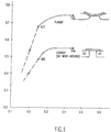
- FIG. 1 Simulated threshold roll-off of devices using two different isolation structures is shown in Figure 1.
- the simulated data shown in Figure 1 was generated assuming that everything else remains the same, such as the same implant condition, oxide thickness, work function, etc.
- the device using recessed oxide isolation (top curve) has the highest threshold voltage, V t . Its long channel (channel length > 0.4 ⁇ m) V t is in the range of 0.6-0.8V.
- the lower curve is for a device with planar shallow trench isolation. Its long channel V t is in the range of 0.4-0.6V.
- One method of achieving acceptable off-current is by increasing the V t by tailored implant to the channel of the FET, particularly along the channel edges that abut the isolation region.
- tailored implant to the channel of the FET, particularly along the channel edges that abut the isolation region.
- V t results in increased V t away from the corners as well as at the corners, with a resultant loss of current drive.
- minimizing corner gate conduction is accomplished by using a gate layout which increases the channel length where the gate crosses over the edge.
- the rest of the gate is maintained at the designed gate length.
- This design guarantees a threshold voltage, V t , in the range of 0.5-0.6V at the corners if corner device channel length is about 0.45 ⁇ m.
- the bulk device has a V t in the range of 0.6-0.7V if channel length is 0.25 ⁇ m. Since a minimum overlay dimension of the longer gate length of the boundaries must be kept at both ends of the device, there is a trade-off with device packing density. These devices can be used for those applications where performance is more important than density.
- a phase shift mask is used to define the resist pattern for the main gate structure.
- This phase shift mask results in a main gate structure which is a very small dimension especially suited to submicron devices. It is, however, this very small dimension which gives rise to the problem of leakage current at the locations where the channel edges abut the isolation structure.
- the invention provides a unique fabrication method which avoids the leakage current problem, which fabrication method can be used for making two FET devices or an FET device with two gates.
- FIG. 1 shows the layout of a conventional FET device wherein a gate 11 is formed over a diffusion region 12 which serves as the source and drain of the FET device.
- the diffusion region 12 is surrounded by an isolation region, generally denoted by the reference numeral 13.
- Figure 3 shows the layout of an FET device according to a preferred embodiment of the invention.
- the gate 14 is enlarged at either end so that the channel length is increased where the gate crosses over the diffusion edge.
- the isolation regions 13 comprises shallow trenches having a depth of between 0.1-0.5 ⁇ .
- One method of achieving the layout shown in Figure 3 is to use a straight-forward mask design with longer gate length at the ends of the device or where the gate crosses over the isolation region, which is also the same at the edge of the gate or boundary gate.
- Another approach, and the one taken by this invention is to use a phase shift mask that contains phase edge patterns in a transparent material to form the main (i.e., shorter) gate and opaque patterns for the boundary (i.e., longer) gate and contact. Since a minimum overlay dimension of the longer gate length of the boundaries must be kept ("d" as shown in Figure 3) at both ends of the device, there is a trade-off of device packing density.
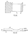
- FIGS 4A to 4C show, in plan view, the process for making the novel mask used to manufacture FET devices according to one aspect of the invention.
- a transparent substrate such as a quartz plate, generally denoted by the reference numeral 20, to be used as a mask.
- the opaque material may be, for example, chromium (Cr).
- a transparent film is applied to the substrate.
- the transparent film may be, for example, a chemical vapor deposited (CVD) blanket of silicon dioxide (SiO2).
- This film is then patterned by etching, such as a reactive ion etch (RIE), to form the phase shift pattern 23 shown in Figure 4B.
- RIE reactive ion etch
- the chrome stripes are etched to the pattern 23 as shown in Figure 4C. Notice from Figure 4C that the chrome and phase shift patterns are thus formed in a self-aligned manner.
- the mask fabrication process is as follows.
- the chrome pattern is defined first.
- a 180° phase shifter such as chemical vapor deposit (CVD) oxide, is then deposited to a thickness of approximately 245 nm. This thickness produces the 180° phase shift at the edges of the pattern for later deep ultraviolet (DUV) exposure.
- the thickness will vary according to the wavelength of the exposure radiation; that is, if shorter wavelengths are used for exposure, then the thickness of the film required to produce a 180° phase shift will be less and, conversely, if longer wavelengths are used, the thickness will be greater.
- the phase shifter patterns are used as a mask to further trim the chrome patterns such that chrome is presented only under the phase shifter patterns as shown in Figure 4C.
- the cross-sectional view of the mask produced in Figure 4C is shown in Figure 4D.
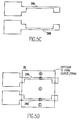
- This mask is used to form the resist pattern 24 on the silicon wafer 25 shown in Figure 5A.
- the main gate structures 26A and 26B are quite narrow since they are defined by the phase edge of the SiO2 on the mask shown in Figure 4C.
- FIG. 5B This block out mask 27 is shown in Figure 5B as a negative (i.e., the pattern area of the mask is etched away).
- FIG 5C This structure is essentially the same as that shown in Figure 3 where the gate structures 26A and 26B are enlarged at either end. As long as the gate length at the boundaries are maintained longer than 0.35 ⁇ m, a V t greater than 0.5V will be established.
- Figure 5D is the same as that of Figure 5C but additionally illustrates the diffusion region 28 which forms the sources and drains of the two FET devices.
- the resulting circuit is shown in Figure 6 and comprises the two FET devices connected in cascade with a common source/drain region C.
- the other parts of the structure shown in Figure 5D which correspond to the circuit shown in Figure 6 are denoted by the nodes A, B, D, and E.
- a two-gate device can be easily designed and fabricated using a phase-edge mask without a block out mask.
- the process uses the same mask as shown in Figure 4C to form the pattern in the wafer shown in Figure 5A; however, the block out mask 27 shown in Figure 5B is not used.
- Final structure of a two-gate device is shown in Figure 7.
- the drain contact is located at the middle and source contacts are on both sides. This device will give about two times of current drive compared to a structure having only one gate. Simulated current-voltage (I-V) characteristics for both single and two-gate devices are shown in Figure 8.
- I-V Simulated current-voltage
- the invention provides several advantages when fabricating submicron FET devices.
- a unique mask structure is provided which uses SiO2 patterned on a transparent substrate, such as a quartz plate.
- the edges of the SiO2 patterns produce a 180° phase shift in UV light used to expose a resist on a silicon wafer during the lithographic exposure, resulting in very narrow channel lengths.
- this mask which includes opaque chromium areas to define enlarged channel lengths at either end of the gate, allows a complete definition of the gate structure with a single exposure and, in addition, permits the direct production of a two-gate structure.
- the fabrication of the mask is facilitated by the self-aligned structure of the SiO2 and chromium patterns.
Landscapes
- Insulated Gate Type Field-Effect Transistor (AREA)
- Preparing Plates And Mask In Photomechanical Process (AREA)
- Exposure Of Semiconductors, Excluding Electron Or Ion Beam Exposure (AREA)
- Exposure And Positioning Against Photoresist Photosensitive Materials (AREA)
- Element Separation (AREA)
Applications Claiming Priority (2)
| Application Number | Priority Date | Filing Date | Title |
|---|---|---|---|
| US27405594A | 1994-07-12 | 1994-07-12 | |
| US274055 | 1994-07-12 |
Publications (2)
| Publication Number | Publication Date |
|---|---|
| EP0692826A2 true EP0692826A2 (fr) | 1996-01-17 |
| EP0692826A3 EP0692826A3 (fr) | 1997-10-01 |
Family
ID=23046574
Family Applications (1)
| Application Number | Title | Priority Date | Filing Date |
|---|---|---|---|
| EP95480073A Withdrawn EP0692826A3 (fr) | 1994-07-12 | 1995-06-09 | Méthode pour supprimer des fuites sous-seuils à cause de coins d'isolation acérés dans des structures FET submicroniques |
Country Status (3)
| Country | Link |
|---|---|
| US (2) | US5567553A (fr) |
| EP (1) | EP0692826A3 (fr) |
| JP (1) | JP3056976B2 (fr) |
Cited By (5)
| Publication number | Priority date | Publication date | Assignee | Title |
|---|---|---|---|---|
| EP0967637A1 (fr) * | 1998-06-24 | 1999-12-29 | Siemens Aktiengesellschaft | Dispositif semi-conducteur et méthode de fabrication |
| EP1501130A1 (fr) * | 2003-07-21 | 2005-01-26 | STMicroelectronics S.r.l. | Dispositif semi-conducteur du type MOS et son procédé de fabrication |
| EP2316126A4 (fr) * | 2008-08-19 | 2013-06-12 | Freescale Semiconductor Inc | Transistor avec compensation de variation de gain |
| CN105593978A (zh) * | 2013-08-30 | 2016-05-18 | 惠普发展公司,有限责任合伙企业 | 半导体设备和制造半导体设备的方法 |
| US20230128785A1 (en) * | 2020-07-14 | 2023-04-27 | Newport Fab, Llc Dba Jazz Semiconductor | Body-Source-Tied Transistor |
Families Citing this family (27)
| Publication number | Priority date | Publication date | Assignee | Title |
|---|---|---|---|---|
| US5573890A (en) * | 1994-07-18 | 1996-11-12 | Advanced Micro Devices, Inc. | Method of optical lithography using phase shift masking |
| US5702976A (en) * | 1995-10-24 | 1997-12-30 | Micron Technology, Inc. | Shallow trench isolation using low dielectric constant insulator |
| JP4138035B2 (ja) * | 1996-08-23 | 2008-08-20 | 株式会社東芝 | 半導体装置 |
| US6228539B1 (en) | 1996-09-18 | 2001-05-08 | Numerical Technologies, Inc. | Phase shifting circuit manufacture method and apparatus |
| US6424010B2 (en) * | 1996-11-15 | 2002-07-23 | Mitsubishi Denki Kabushiki Kaisha | Method of manufacturing a semiconductor device having reduced power consumption without a reduction in the source/drain breakdown voltage |
| JPH10154732A (ja) * | 1996-11-22 | 1998-06-09 | Mitsubishi Electric Corp | 半導体素子分離端欠陥評価テスト構造および該テスト構造を用いた評価方法 |
| JPH10256394A (ja) | 1997-03-12 | 1998-09-25 | Internatl Business Mach Corp <Ibm> | 半導体構造体およびデバイス |
| JP3528554B2 (ja) * | 1997-12-04 | 2004-05-17 | セイコーエプソン株式会社 | 半導体装置 |
| US6001706A (en) * | 1997-12-08 | 1999-12-14 | Chartered Semiconductor Manufacturing, Ltd. | Method for making improved shallow trench isolation for semiconductor integrated circuits |
| US5880006A (en) * | 1998-05-22 | 1999-03-09 | Vlsi Technology, Inc. | Method for fabrication of a semiconductor device |
| US6518145B1 (en) | 1998-08-06 | 2003-02-11 | International Business Machines Corporation | Methods to control the threshold voltage of a deep trench corner device |
| US6236258B1 (en) | 1998-08-25 | 2001-05-22 | International Business Machines Corporation | Wordline driver circuit using ring-shaped devices |
| US5998848A (en) * | 1998-09-18 | 1999-12-07 | International Business Machines Corporation | Depleted poly-silicon edged MOSFET structure and method |
| US6265120B1 (en) | 2000-02-01 | 2001-07-24 | Taiwan Semiconductor Manufacturing Company | Geometry design of active region to improve junction breakdown and field isolation in STI process |
| JP4142228B2 (ja) * | 2000-02-01 | 2008-09-03 | 株式会社ルネサステクノロジ | 半導体集積回路装置 |
| JP2002118176A (ja) * | 2000-10-05 | 2002-04-19 | Nec Corp | 半導体装置 |
| JP2002222944A (ja) * | 2001-01-26 | 2002-08-09 | Kitakiyuushiyuu Techno Center:Kk | 半導体素子 |
| JP2004529378A (ja) * | 2001-03-08 | 2004-09-24 | ニューメリカル テクノロジーズ インコーポレイテッド | 多重レベルのマスキング解像度用の交番位相偏移マスキング |
| US20040099891A1 (en) * | 2001-10-25 | 2004-05-27 | Manoj Mehrotra | Sub-critical-dimension integrated circuit features |
| JP4142312B2 (ja) * | 2002-02-28 | 2008-09-03 | ハリマ化成株式会社 | 析出型はんだ組成物及びはんだ析出方法 |
| JP4603248B2 (ja) * | 2003-06-19 | 2010-12-22 | 株式会社Kenzan | 半導体素子およびそれを備えた論理回路 |
| KR100525111B1 (ko) * | 2004-04-19 | 2005-11-01 | 주식회사 하이닉스반도체 | 반도체 소자 |
| US7323746B2 (en) * | 2004-09-14 | 2008-01-29 | Samsung Electronics Co., Ltd. | Recess gate-type semiconductor device and method of manufacturing the same |
| JP4851718B2 (ja) * | 2005-01-28 | 2012-01-11 | 株式会社東芝 | 半導体装置 |
| US7704850B2 (en) * | 2006-09-08 | 2010-04-27 | Asml Netherlands B.V. | Semiconductor device for measuring an overlay error, method for measuring an overlay error, lithographic apparatus and device manufacturing method |
| JP5270876B2 (ja) * | 2007-08-22 | 2013-08-21 | セイコーインスツル株式会社 | 半導体装置 |
| JP5465907B2 (ja) * | 2009-03-27 | 2014-04-09 | ラピスセミコンダクタ株式会社 | 半導体装置 |
Family Cites Families (24)
| Publication number | Priority date | Publication date | Assignee | Title |
|---|---|---|---|---|
| JPS56118349A (en) * | 1980-02-22 | 1981-09-17 | Fujitsu Ltd | Semiconductor device |
| DE3174468D1 (en) * | 1980-09-17 | 1986-05-28 | Hitachi Ltd | Semiconductor device and method of manufacturing the same |
| JPS5827363A (ja) * | 1981-08-10 | 1983-02-18 | Fujitsu Ltd | 電界効果トランジスタの製造法 |
| JPS6081867A (ja) * | 1983-10-11 | 1985-05-09 | Nec Corp | Mos型電界効果トランジスタ |
| JPH0618263B2 (ja) * | 1984-02-23 | 1994-03-09 | 日本電気株式会社 | 電荷転送素子 |
| JPS6119174A (ja) * | 1984-07-06 | 1986-01-28 | Toshiba Corp | 半導体装置 |
| US5061654A (en) * | 1987-07-01 | 1991-10-29 | Mitsubishi Denki Kabushiki Kaisha | Semiconductor integrated circuit having oxide regions with different thickness |
| JPH0770721B2 (ja) * | 1988-07-06 | 1995-07-31 | 株式会社東芝 | 半導体装置 |
| JPH0268963A (ja) * | 1988-09-02 | 1990-03-08 | Matsushita Electron Corp | 電界効果トランジスタ |
| US5248894A (en) * | 1989-10-03 | 1993-09-28 | Harris Corporation | Self-aligned channel stop for trench-isolated island |
| EP0445471A3 (en) * | 1990-03-06 | 1994-10-26 | Digital Equipment Corp | Method of forming isolation trenches in a semiconductor substrate |
| JPH04130774A (ja) * | 1990-09-21 | 1992-05-01 | Mitsubishi Electric Corp | 半導体装置の製造方法 |
| JPH04196478A (ja) * | 1990-11-28 | 1992-07-16 | Seiko Epson Corp | 薄膜半導体装置 |
| US5250837A (en) * | 1991-05-17 | 1993-10-05 | Delco Electronics Corporation | Method for dielectrically isolating integrated circuits using doped oxide sidewalls |
| US5330879A (en) * | 1992-07-16 | 1994-07-19 | Micron Technology, Inc. | Method for fabrication of close-tolerance lines and sharp emission tips on a semiconductor wafer |
| JPH0643646A (ja) * | 1992-07-24 | 1994-02-18 | Kawasaki Steel Corp | フォトレジスト組成物 |
| JPH0653493A (ja) * | 1992-07-31 | 1994-02-25 | Kawasaki Steel Corp | 半導体装置 |
| JPH0661481A (ja) * | 1992-08-04 | 1994-03-04 | Matsushita Electron Corp | Mos型半導体装置 |
| JP2886420B2 (ja) * | 1992-10-23 | 1999-04-26 | 三菱電機株式会社 | 半導体装置の製造方法 |
| US5275965A (en) * | 1992-11-25 | 1994-01-04 | Micron Semiconductor, Inc. | Trench isolation using gated sidewalls |
| JPH07115190A (ja) * | 1992-11-30 | 1995-05-02 | Texas Instr Inc <Ti> | ゲート画定トランジスタ |
| US5313419A (en) * | 1993-02-01 | 1994-05-17 | National Semiconductor Corporation | Self-aligned trench isolation scheme for select transistors in an alternate metal virtual ground (AMG) EPROM array |
| US5494857A (en) * | 1993-07-28 | 1996-02-27 | Digital Equipment Corporation | Chemical mechanical planarization of shallow trenches in semiconductor substrates |
| US5465859A (en) * | 1994-04-28 | 1995-11-14 | International Business Machines Corporation | Dual phase and hybrid phase shifting mask fabrication using a surface etch monitoring technique |
-
1995
- 1995-05-18 US US08/447,571 patent/US5567553A/en not_active Expired - Fee Related
- 1995-06-09 EP EP95480073A patent/EP0692826A3/fr not_active Withdrawn
- 1995-07-10 JP JP17370995A patent/JP3056976B2/ja not_active Expired - Fee Related
- 1995-10-11 US US08/540,961 patent/US6144081A/en not_active Expired - Fee Related
Non-Patent Citations (1)
| Title |
|---|
| None |
Cited By (10)
| Publication number | Priority date | Publication date | Assignee | Title |
|---|---|---|---|---|
| EP0967637A1 (fr) * | 1998-06-24 | 1999-12-29 | Siemens Aktiengesellschaft | Dispositif semi-conducteur et méthode de fabrication |
| EP1501130A1 (fr) * | 2003-07-21 | 2005-01-26 | STMicroelectronics S.r.l. | Dispositif semi-conducteur du type MOS et son procédé de fabrication |
| EP2316126A4 (fr) * | 2008-08-19 | 2013-06-12 | Freescale Semiconductor Inc | Transistor avec compensation de variation de gain |
| CN105593978A (zh) * | 2013-08-30 | 2016-05-18 | 惠普发展公司,有限责任合伙企业 | 半导体设备和制造半导体设备的方法 |
| EP3039712A4 (fr) * | 2013-08-30 | 2017-03-29 | Hewlett-Packard Development Company, L.P. | Dispositif à semi-conducteurs et son procédé de fabrication |
| US9786777B2 (en) | 2013-08-30 | 2017-10-10 | Hewlett-Packard Development Company, L.P. | Semiconductor device and method of making same |
| US10084062B2 (en) | 2013-08-30 | 2018-09-25 | Hewlett-Packard Development Company, L.P. | Semiconductor device comprising a gate formed from a gate ring |
| CN105593978B (zh) * | 2013-08-30 | 2019-05-31 | 惠普发展公司,有限责任合伙企业 | 半导体设备和制造半导体设备的方法 |
| US20230128785A1 (en) * | 2020-07-14 | 2023-04-27 | Newport Fab, Llc Dba Jazz Semiconductor | Body-Source-Tied Transistor |
| US12568801B2 (en) * | 2020-07-14 | 2026-03-03 | Newport Fab, Llc | Body-source-tied transistor |
Also Published As
| Publication number | Publication date |
|---|---|
| JPH0855985A (ja) | 1996-02-27 |
| EP0692826A3 (fr) | 1997-10-01 |
| JP3056976B2 (ja) | 2000-06-26 |
| US5567553A (en) | 1996-10-22 |
| US6144081A (en) | 2000-11-07 |
Similar Documents
| Publication | Publication Date | Title |
|---|---|---|
| US5567553A (en) | Method to suppress subthreshold leakage due to sharp isolation corners in submicron FET structures | |
| US6306547B1 (en) | Photomask and manufacturing method thereof, and exposure method using the photomask | |
| US6479398B1 (en) | Method of manufacturing an amorphous-silicon thin film transistor | |
| US6686300B2 (en) | Sub-critical-dimension integrated circuit features | |
| US5240869A (en) | Method for fabricating a field effect transistor | |
| KR100348902B1 (ko) | 에이치이엠티의 감마게이트 제조방법 | |
| US5942787A (en) | Small gate electrode MOSFET | |
| US5757028A (en) | Thin film transistor with reduced leakage current | |
| US5693548A (en) | Method for making T-gate of field effect transistor | |
| US7419767B2 (en) | Phase-shifting mask and method of forming pattern using the same | |
| JP2610402B2 (ja) | 二重露光によるt形のゲートの製造方法 | |
| JPH02271537A (ja) | 半導体装置及びその製造方法 | |
| US20040099891A1 (en) | Sub-critical-dimension integrated circuit features | |
| EP0978869B1 (fr) | Procédé pour fabriquer un motif de photoréserve minuscule et procédé pour fabriquer une électrode grille | |
| JP3419603B2 (ja) | 半導体装置の製造方法 | |
| US20030096465A1 (en) | Hard mask trimming with thin hard mask layer and top protection layer | |
| JPH0815161B2 (ja) | 半導体装置の製造方法 | |
| JP3004821B2 (ja) | 電極の形成方法 | |
| JP2807122B2 (ja) | 薄膜トランジスタの製造方法 | |
| KR100300862B1 (ko) | 박막트랜지스터제조방법 | |
| KR0171736B1 (ko) | 전계효과트랜지스터 제조 방법 | |
| KR950005490B1 (ko) | 인헨스먼트형/디플리션형 전계효과 트랜지스터 및 그 제조방법 | |
| KR100824198B1 (ko) | 반도체 소자의 제조방법 | |
| JPH05218095A (ja) | 半導体装置の製造方法 | |
| KR960019741A (ko) | 에스램(sram) 셀 및 그 제조방법 |
Legal Events
| Date | Code | Title | Description |
|---|---|---|---|
| PUAI | Public reference made under article 153(3) epc to a published international application that has entered the european phase |
Free format text: ORIGINAL CODE: 0009012 |
|
| AK | Designated contracting states |
Kind code of ref document: A2 Designated state(s): DE FR GB |
|
| PUAL | Search report despatched |
Free format text: ORIGINAL CODE: 0009013 |
|
| AK | Designated contracting states |
Kind code of ref document: A3 Designated state(s): DE FR GB |
|
| STAA | Information on the status of an ep patent application or granted ep patent |
Free format text: STATUS: THE APPLICATION IS DEEMED TO BE WITHDRAWN |
|
| 18D | Application deemed to be withdrawn |
Effective date: 19980103 |